WO2019146372A1 - Dispositif d'entrée - Google Patents
Dispositif d'entrée Download PDFInfo
- Publication number
- WO2019146372A1 WO2019146372A1 PCT/JP2018/048208 JP2018048208W WO2019146372A1 WO 2019146372 A1 WO2019146372 A1 WO 2019146372A1 JP 2018048208 W JP2018048208 W JP 2018048208W WO 2019146372 A1 WO2019146372 A1 WO 2019146372A1
- Authority
- WO
- WIPO (PCT)
- Prior art keywords
- adhesion
- convex surface
- area
- input device
- main body
- Prior art date
- Legal status (The legal status is an assumption and is not a legal conclusion. Google has not performed a legal analysis and makes no representation as to the accuracy of the status listed.)
- Ceased
Links
Images

Classifications
-
- G—PHYSICS
- G06—COMPUTING OR CALCULATING; COUNTING
- G06F—ELECTRIC DIGITAL DATA PROCESSING
- G06F3/00—Input arrangements for transferring data to be processed into a form capable of being handled by the computer; Output arrangements for transferring data from processing unit to output unit, e.g. interface arrangements
- G06F3/01—Input arrangements or combined input and output arrangements for interaction between user and computer
- G06F3/03—Arrangements for converting the position or the displacement of a member into a coded form
- G06F3/041—Digitisers, e.g. for touch screens or touch pads, characterised by the transducing means
-
- G—PHYSICS
- G06—COMPUTING OR CALCULATING; COUNTING
- G06F—ELECTRIC DIGITAL DATA PROCESSING
- G06F3/00—Input arrangements for transferring data to be processed into a form capable of being handled by the computer; Output arrangements for transferring data from processing unit to output unit, e.g. interface arrangements
- G06F3/01—Input arrangements or combined input and output arrangements for interaction between user and computer
- G06F3/03—Arrangements for converting the position or the displacement of a member into a coded form
- G06F3/041—Digitisers, e.g. for touch screens or touch pads, characterised by the transducing means
- G06F3/044—Digitisers, e.g. for touch screens or touch pads, characterised by the transducing means by capacitive means
-
- G—PHYSICS
- G06—COMPUTING OR CALCULATING; COUNTING
- G06F—ELECTRIC DIGITAL DATA PROCESSING
- G06F3/00—Input arrangements for transferring data to be processed into a form capable of being handled by the computer; Output arrangements for transferring data from processing unit to output unit, e.g. interface arrangements
- G06F3/01—Input arrangements or combined input and output arrangements for interaction between user and computer
- G06F3/03—Arrangements for converting the position or the displacement of a member into a coded form
- G06F3/041—Digitisers, e.g. for touch screens or touch pads, characterised by the transducing means
- G06F3/044—Digitisers, e.g. for touch screens or touch pads, characterised by the transducing means by capacitive means
- G06F3/0446—Digitisers, e.g. for touch screens or touch pads, characterised by the transducing means by capacitive means using a grid-like structure of electrodes in at least two directions, e.g. using row and column electrodes
-
- B—PERFORMING OPERATIONS; TRANSPORTING
- B32—LAYERED PRODUCTS
- B32B—LAYERED PRODUCTS, i.e. PRODUCTS BUILT-UP OF STRATA OF FLAT OR NON-FLAT, e.g. CELLULAR OR HONEYCOMB, FORM
- B32B7/00—Layered products characterised by the relation between layers; Layered products characterised by the relative orientation of features between layers, or by the relative values of a measurable parameter between layers, i.e. products comprising layers having different physical, chemical or physicochemical properties; Layered products characterised by the interconnection of layers
- B32B7/04—Interconnection of layers
- B32B7/12—Interconnection of layers using interposed adhesives or interposed materials with bonding properties
-
- C—CHEMISTRY; METALLURGY
- C09—DYES; PAINTS; POLISHES; NATURAL RESINS; ADHESIVES; COMPOSITIONS NOT OTHERWISE PROVIDED FOR; APPLICATIONS OF MATERIALS NOT OTHERWISE PROVIDED FOR
- C09D—COATING COMPOSITIONS, e.g. PAINTS, VARNISHES OR LACQUERS; FILLING PASTES; CHEMICAL PAINT OR INK REMOVERS; INKS; CORRECTING FLUIDS; WOODSTAINS; PASTES OR SOLIDS FOR COLOURING OR PRINTING; USE OF MATERIALS THEREFOR
- C09D5/00—Coating compositions, e.g. paints, varnishes or lacquers, characterised by their physical nature or the effects produced; Filling pastes
-
- B—PERFORMING OPERATIONS; TRANSPORTING
- B32—LAYERED PRODUCTS
- B32B—LAYERED PRODUCTS, i.e. PRODUCTS BUILT-UP OF STRATA OF FLAT OR NON-FLAT, e.g. CELLULAR OR HONEYCOMB, FORM
- B32B2457/00—Electrical equipment
- B32B2457/20—Displays, e.g. liquid crystal displays, plasma displays
- B32B2457/208—Touch screens
-
- G—PHYSICS
- G06—COMPUTING OR CALCULATING; COUNTING
- G06F—ELECTRIC DIGITAL DATA PROCESSING
- G06F2203/00—Indexing scheme relating to G06F3/00 - G06F3/048
- G06F2203/041—Indexing scheme relating to G06F3/041 - G06F3/045
- G06F2203/04102—Flexible digitiser, i.e. constructional details for allowing the whole digitising part of a device to be flexed or rolled like a sheet of paper
-
- G—PHYSICS
- G06—COMPUTING OR CALCULATING; COUNTING
- G06F—ELECTRIC DIGITAL DATA PROCESSING
- G06F2203/00—Indexing scheme relating to G06F3/00 - G06F3/048
- G06F2203/041—Indexing scheme relating to G06F3/041 - G06F3/045
- G06F2203/04103—Manufacturing, i.e. details related to manufacturing processes specially suited for touch sensitive devices
Definitions
- the present invention relates to an input device, and more particularly to an input device provided with a film sensor that detects a position where a finger or the like approaches.
- a film sensor that is often used as an input device includes a sensor that detects a position at which a finger or the like approaches a detection area (hereinafter, the approach includes a touch).
- the approach includes a touch.
- an electrode on the drive side and an electrode on the output side are provided, a drive pulse is applied to the electrode on the drive side, and a capacitance change caused by a finger or the like is detected by the electrode on the output side. It is detected.
- a film sensor is attached to a cover member having a convex surface.
- transparent adhesive layers such as OCA (Optical Clear Adhesive) are used.
- Patent Document 1 discloses a touch sensor that can be easily installed in three dimensions according to an electronic device having a three-dimensional shape for the attachment of a film sensor.
- this touch sensor notches are formed in the right side electrode area and the left side electrode area of the PET film, and the stress concentrated on the electrode and the signal line is dispersed at the time of bending.
- Patent Document 2 discloses a sticking tool to be stuck on a curved surface and a sticking method thereof.
- This sticking tool has a sticking material to be stuck on a curved surface of a body to be bonded, a pressure-sensitive adhesive added to the back surface, and a release paper added to the back surface of the pressure-sensitive adhesive. Slits for preventing wrinkles are formed on two opposing sides extending from one end to the other end of the adhesive.
- Patent Document 3 discloses a flexible printed circuit board, a method of adhering a flexible printed circuit board, and an electronic device capable of preventing the occurrence of wrinkles when the flexible printed circuit board is pasted to an adherend having a cubic curved surface.
- a substantially arc-shaped notch is formed at the periphery of the flexible printed circuit board, particularly at a portion where strain stress tends to be concentrated at the time of bonding.
- the film sensor When the film sensor is attached to a curved surface, bending stress is likely to be concentrated at a portion (for example, an extension of the substrate) which is apart from the bonding portion with the curved surface in the substrate of the film sensor.
- a portion for example, an extension of the substrate
- the position where the bending stress is concentrated is placed on the electrode of the sensor or the lead-out wire, it causes the occurrence of a crack in the electrode or the lead-out wire and disconnection.
- the film sensor when the film sensor is attached to a curved surface, the film sensor needs to be strongly bonded as compared to the case where the film sensor is attached to a flat surface.
- An object of the present invention is to provide an input device capable of suppressing the damage to the electrode by reducing the edge effect of the end face of the adhesive layer in affixing the film sensor to the convex surface.
- one mode of the present invention is an input device provided with a film sensor and a cover member which has a convex.
- the film sensor includes a support base having a film-like main body and an extension extending outward from an edge of the main body, and a plurality of electrodes provided on the surface of the main body. And a lead-out pattern electrically connected to each of the plurality of electrode parts and extending from the main body part to the extension part.
- the surface of the main body on which the plurality of electrodes are located is attached to the convex surface through the adhesive layer.
- the adhesion of the end adhesive area located on the extension side of the adhesive layer is lower than that of the central adhesive area located on the central side of the convex surface of the adhesive layer.
- the adhesion of the end adhesion area in the adhesion layer is lower than the adhesion of the central adhesion area, so that the boundary between the part adhered with the adhesion layer and the part not adhered in the supporting substrate It is possible to suppress the abrupt change of the adhesive strength of Thereby, when affixing a film sensor to the cover member which has a convex surface, the edge effect in the contact bonding layer edge part of the curved support base material can be reduced.
- the bonding area per unit area of the end bonding area may be smaller than the bonding area per unit area of the central bonding area. Therefore, a sharp change of the adhesive strength from the central adhesion region to the end adhesion region is suppressed.
- connection area located on the extension side of the main body may be located away from the convex surface as it approaches the end of the main body. Thereby, the rapid change of the bending in the connection area in the main body portion is suppressed.
- the end adhesion area in the adhesive layer may have an adhesive taper area in which the adhesion decreases as the distance between the film sensor and the convex surface increases.
- the separation distance between the film sensor and the convex surface may be increased and the amount of the adhesive forming the adhesive layer may be reduced. Thereby, the adhesiveness by the adhesive layer toward the extension part side of a main-body part falls gradually, and the steep change of adhesive force is suppressed.
- the separation distance between the film sensor and the convex surface is increased and the area of the adhesive layer in contact with both the film sensor and the convex surface is reduced as viewed from the normal direction of the convex surface. It may be done. Thereby, the adhesiveness by the adhesive layer toward the extension part side of a main-body part falls gradually, and the steep change of adhesive force is suppressed.
- the end of the adhesive layer in the adhesion decreasing area, may have a non-linear portion as viewed from the normal direction of the convex surface.
- the adhesive layer may be provided so as to be attached to the entire electrode region where the plurality of electrode units are provided.
- strong adhesion can be performed on the surface provided with the plurality of electrode portions of the main body portion, and the adhesive strength toward the extension portion side of the main body portion is steep due to the end adhesion region. Changes can also be suppressed.
- the input device which can reduce the edge effect of the edge part of the contact bonding layer, and can suppress the damage to an electrode in affixing the film sensor to a convex surface.
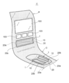
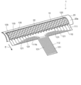
- FIG. 1 It is a schematic diagram which shows the application example of the input device which concerns on this embodiment. It is a perspective view which illustrates the input device concerning this embodiment. It is the model top view which expanded a part of electrode part and adhesive layer.
- (A) And (b) is a schematic cross section of the input device concerning this embodiment.
- (A) and (b) are schematic diagrams illustrating a reference example.
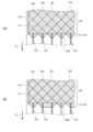
- (A) And (b) is a schematic diagram which shows the example of another edge part adhesion
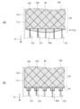
- (A) And (b) is a schematic diagram which shows the example of another edge part adhesion
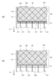
- A) And (b) is a schematic diagram which shows the example of another edge part adhesion
- FIG. 1 is a schematic view showing an application example of the input device according to the present embodiment.
- FIG. 2 is a perspective view illustrating the input device according to the present embodiment.
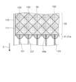
- FIG. 3 is a schematic plan view in which a part of the electrode portion and the adhesive layer is enlarged.
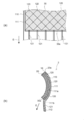
- FIGS. 4A and 4B are schematic cross-sectional views of the input device according to the present embodiment.
- FIG. 4A shows a cross-sectional view in the longitudinal direction
- FIG. 4B shows a partially enlarged cross-sectional view of the connection area.
- the input device 1 is a touch detection device that detects a position at which a finger or the like approaches a detection region.
- the input device 1 includes a film sensor 10 and a cover member 20 having a convex surface 20a.
- the input device 1 is provided, for example, on a back side of an instrument panel P provided with the display device 100 and the switch 103 and a panel such as a floor console C in a mobile unit V such as an automobile shown in FIG.
- the input device 1 is provided in a portion that receives a predetermined operation using a finger or the like.
- a cover member 20 is provided on the instrument panel P and the floor console C.
- the cover member 20 is provided with a concave surface 20b for contacting a finger.
- the concave surface 20b may be provided in a straight line so as to facilitate tracing while touching the inside of a finger, or a predetermined width and length so as to facilitate tracing on a surface while bringing one or more fingers into contact. It may be provided in an area having
- the back surface side (opposite side) of the concave surface 20b of the cover member 20 is a convex surface 20a.
- the convex surface 20a has a shape in which an arc extends in a plane.
- the direction in which the arc of the convex surface 20a extends is referred to as the length direction, and the direction along the arc is referred to as the width direction.
- the film sensor 10 is mounted along the convex surface 20a.
- the film sensor 10 is, for example, a capacitive touch sensor, and performs position detection by reading a change in electrostatic capacitance when a finger or the like approaches the concave surface 20b on the convex surface 20a side.
- the concave surface 20b side of the cover member 20 is a front surface to be seen by the operator, and the convex surface 20a side of the cover member 20 is a back surface, and the input device 1 is arranged to be invisible to the operator.
- the film sensor 10 has a support base 110, a plurality of electrode portions 120, and a lead pattern 121.
- the support substrate 110 is formed of a flexible film such as PET (polyethylene terephtalate), COP (cycloolefin polymer), COC (cyclic olefin copolymer) or the like.
- the support base 110 may have translucency.
- the support base 110 has a film-like main body portion 111 and an extension portion 112 extending outward E from an end portion 111 b of the main body portion 111.
- the main body portion 111 is provided corresponding to the shape of the convex surface 20 a of the cover member 20. That is, the main body portion 111 has a size that constitutes a detection area for detecting the approach position of the finger corresponding to the width direction and the length direction of the concave surface 20b.
- the extension portion 112 is a portion extending from a part of the end portion 111b of the main body portion 111 by a predetermined length, for example. In the example shown in FIG. 2, the extension portion 112 extends from a part of the central portion of the end portion 111 b of the main body portion 111. The extension portion 112 may extend from a portion other than the central portion of the end portion 111b, or may extend from the entire end portion 111b.
- the plurality of electrode units 120 are provided on the surface 111 a (see FIG. 4) on the convex surface 20 a side of the main body unit 111.
- a plurality of island-shaped electrode portions 120 are arranged vertically and horizontally along the surface 111a.
- the pattern shape of the electrode part 120 and a position detection system are not limited to this.
- the plurality of electrode units 120 When transmitting light from the display unit or the light source to the front side from the back surface side of the cover member 20, the plurality of electrode units 120 are formed of a translucent conductive material. Further, since the plurality of electrode portions 120 are bent along the convex surface 20a, a relatively flexible material of the light-transmitting conductive materials is used. Therefore, as the plurality of electrode portions 120, translucent conductive oxides such as ITO (Indium Tin Oxide), SnO 2 , and ZnO are preferable.
- ITO Indium Tin Oxide
- SnO 2 Tin Oxide
- ZnO ZnO
- the lead-out pattern 121 is a pattern which is conducted to each of the plurality of electrode parts 120 and drawn from the main body part 111 to the extension part 112. In order to obtain continuity with the plurality of electrode units 120 arranged in a predetermined range along the surface 111 a of the main body unit 111, the lead-out pattern 121 is drawn along the surface 111 a while being conducted with each of the plurality of electrode units 120. , To the extension unit 112. Pads and connectors (not shown) electrically connected to the respective lead-out patterns 121 are provided at the tip of the extension part 112, and connection with external devices and circuits is performed.
- Such a film sensor 10 is attached to the convex surface 20 a of the cover member 20 via the adhesive layer 30 on the surface 111 a on the side where the plurality of electrode parts 120 of the main body part 111 are located.
- the adhesive layer 30 a translucent adhesive such as OCA (Optical Clear Adhesive) is used. However, when it is not necessary to have translucency, a colored adhesive may be used.
- the adhesive layer 30 is preferably provided so as to be attached to the entire electrode region where the plurality of electrode units 120 are provided. As a result, strong bonding can be performed on the surface 111 a on which the plurality of electrode units 120 of the main body unit 111 are provided.
- the adhesive layer 30 has an end adhesive area 31 located on the extension 112 side and a central adhesive area 32 located on the central side of the convex surface 20 a.
- the end adhesion area 31 is an area where the predetermined width area is adhered from the end of the electrode section 120 on the side of the extension 112.
- the end adhesion region 31 may also cover a part of the lead-out pattern 121 connected to the end of the electrode portion 120.
- the central bonding region 32 is a region for bonding a predetermined width region located closer to the central portion (opposite to the extending portion 112) than the end bonding region 31.
- the bonding area other than the end bonding area 31 may be the central bonding area 32.
- the adhesion of the end adhesion area 31 is set to be lower than the adhesion of the central adhesion area 32.
- a sharp change in the adhesive strength at the boundary between the portion bonded to the convex surface 20 a by the adhesive layer 30 and the portion not bonded to the support base 110 is suppressed. Therefore, when the film sensor 10 is attached to the cover member 20 having the convex surface 20a, the edge effect (stress concentration at the edge) at the end 30a of the adhesive layer 30 of the curved support substrate 110 can be reduced.
- the end adhesion area 31 may be provided with an adhesive decreasing area 31 a.
- the adhesion decreasing area 31a is an area in which the adhesion decreases as the distance between the film sensor 10 and the convex surface 20a increases. Due to this adhesive gradual decrease area 31a, the adhesiveness by the adhesive layer 30 toward the extension portion 112 side of the main body 111 is gradually lowered outward, and a sharp change in adhesive strength is suppressed.
- the end 30 a of the adhesive layer 30 is not linear but uneven.
- a concavo-convex shape of the end portion 30a a convex portion protrudes outward in a semicircular shape.
- a plurality of convex portions are provided at predetermined intervals. Between adjacent convex parts is a recessed part, and the bottom of the recessed part is linear.
- the main body 111 of the support base 110 is curved along the convex surface 20a.
- the surface 111a on which the plurality of electrode portions 120 in the main body portion 111 are formed is concavely curved along the convex surface 20a.
- a portion of the support base 110 which is not adhered by the adhesive layer 30 (the extension 112 and the end 111b of the main body 111) is not pulled toward the convex surface 20a.
- the portion of the support base 110 which is not adhered by the adhesive layer 30 can be curved in the direction in which the extension 112 is routed.
- the adhesion of the end adhesion area 31 is set to be lower than the adhesion of the central adhesion area 32 so that adhesion is performed by the adhesion layer 30 in the support base 110.
- the portion which is not bent is curved, the sharp bending at the end 30 a of the adhesive layer 30 is suppressed.
- the support base 110 has a main body portion 111 and an extension portion 112, and the extension portion 112 is outward E from the end portion 111b of the main body portion 111. It is extended to An adhesive layer 30 is interposed between the main body portion 111 and the convex surface 20a.
- the connection region 111 c located on the side of the extension portion 112 in the main body portion 111 is provided to be separated from the convex surface 20 a as it approaches the end portion 111 b of the main body portion 111.
- the distance d between the surface 111a of the main body 111 and the convex surface 20a becomes more outward E (the end 111b The closer you are to
- the sharp bending of the support base 110 from the connection region 111c to the extension 112 is suppressed, and the stress concentration due to the bending in this portion is relaxed.
- rapid bending of the electrode portion 120 and the lead-out pattern 121 provided at this position is suppressed, and generation of cracks and breakage due to bending of the electrode portion 120 and the lead-out pattern 121 is prevented.
- FIG. 5 is a schematic view illustrating a reference example.
- 5 (a) shows a partially enlarged plan view of the electrode portion 120 and the adhesive layer 30, and
- FIG. 5 (b) shows a cross-sectional view of the input device 2 as viewed in the longitudinal direction of the cover member 20.
- the end 30a on the extension 112 side is provided linearly in the length direction.
- the support substrate 110 is attached to the convex surface 20 a by the adhesive layer 30 with uniform adhesion. Therefore, the area of the support base 110 attached to the convex surface 20a is attached along the convex surface 20a with strong and uniform adhesive force.
- the adhesive strength does not work at all, so the abrupt change in adhesive strength with the end 30a as a boundary Will occur.
- the support base 110 When the extension portion 112 is curved with respect to the main body portion 111, the support base 110 is bent around the linear end 30a of the adhesive layer 30. Under the present circumstances, the support base material 110 becomes easy to bend rapidly by the boundary (end part 30a of the contact bonding layer 30) of the part curved and attached along the convex surface 20a, and the part without the contact bonding layer 30. FIG. When the support base 110 is sharply bent, stress is concentrated on the bent portion of the electrode portion 120 and the lead-out pattern 121 (edge effect), and the occurrence of a crack or disconnection easily occurs.
- the adhesion of the end adhesion area 31 is lower than the adhesion of the central adhesion area 32, so that the abrupt change in adhesion at the end 30a of the adhesion layer 30 does not occur, and the reference example
- the support base 110 bends gently as compared with FIG. For this reason, the occurrence of a crack or disconnection due to bending of the electrode portion 120 or the lead-out pattern 121 is effectively prevented.
- Example of other end adhesion area 6 (a) to 8 (b) are schematic diagrams showing examples of other end adhesion regions.
- the end 30a is provided in a corrugated uneven shape.
- the uneven shape of the end portion 30a is a smooth curve and has a shape in which the convex portion and the concave portion are continuous.
- a convex portion which is a smooth curve and a linear convex portion are repeated as the uneven shape of the end 30a. Even with such a shape, an adhesive gradually decreasing area 31a in which the adhesive strength gradually decreases outward is formed. In this example, the adhesive strength of the adhesive decreasing area 31a can be adjusted by the length of the linear convex portion.
- the end 30a is provided in a large curved shape (non-linear shape) when viewed in the normal direction of the convex surface 20a. That is, since the end 30 a has a large curved shape (non-linear shape), the adhesive gradual decrease area 31 a is formed in the end adhesion area 31.
- the end 30a is provided in a rectangular uneven shape. Since the end 30a has a rectangular uneven shape, no adhesive force is generated in the recess, and the adhesive force of the end adhesive region 31 can be lower than the adhesive force of the central adhesive region 32. .
- the adhesive strength of the end adhesion area 31 can be adjusted by the size and pitch of the uneven shape of the end 30a.
- a dot-like adhesion area 311 is provided in the length direction.
- the dot-like bonding area 311 has a circular shape, but may have a shape other than the circular shape. Due to such a dot-like bonding area 311, the amount of bonding material per unit area in the end bonding area 31 is smaller than that in the central bonding area 32, and the adhesion of the end bonding area 31 can be The adhesion of the adhesion area 32 can be reduced.
- the adhesive strength of the adhesive gradual decrease area 31 a can be adjusted by the size and the pitch of the dot-like adhesive area 311.
- an adhesive material in which the adhesive strength of the end adhesive area 31 is lower than that of the central adhesive area 32 is used. Even if the bonding material of the end bonding area 31 and the bonding material of the central bonding area 32 are the same as each other, even if the bonding strength is reduced only at the end bonding area 31 (for example, electron beam irradiation) Good.
- the edge effect of the end 30 a of the adhesive layer 30 is reduced to bend the support base 110.
- the input device 1 capable of suppressing damage such as cracking or disconnection of the electrode portion 120 or the lead-out pattern 121 due to the above.
- the end bonding area 31 can be formed only by making the shape of the end 30a non-linear, and it becomes possible to reduce the edge effect without going through complicated manufacturing processes.
- switch 110 support base material 111: main body portion 111a: surface 111b: end portion 111c: connection region 112: extension portion 120: electrode portion 121: extraction pattern 311: adhesion region C: floor console d: interval E: outside P: Instrument panel V: Mobile
Landscapes
- Engineering & Computer Science (AREA)
- General Engineering & Computer Science (AREA)
- Theoretical Computer Science (AREA)
- General Physics & Mathematics (AREA)
- Human Computer Interaction (AREA)
- Physics & Mathematics (AREA)
- Chemical & Material Sciences (AREA)
- Wood Science & Technology (AREA)
- Organic Chemistry (AREA)
- Materials Engineering (AREA)
- Life Sciences & Earth Sciences (AREA)
- Position Input By Displaying (AREA)
- Laminated Bodies (AREA)
Abstract
Priority Applications (5)
| Application Number | Priority Date | Filing Date | Title |
|---|---|---|---|
| CN201890001496.6U CN212460527U (zh) | 2018-01-26 | 2018-12-27 | 输入装置 |
| KR1020207018074A KR102361070B1 (ko) | 2018-01-26 | 2018-12-27 | 입력 장치 |
| DE212018000394.7U DE212018000394U1 (de) | 2018-01-26 | 2018-12-27 | Eingabevorrichtung |
| JP2019567944A JP6870120B2 (ja) | 2018-01-26 | 2018-12-27 | 入力装置 |
| US16/926,101 US11188182B2 (en) | 2018-01-26 | 2020-07-10 | Input device |
Applications Claiming Priority (2)
| Application Number | Priority Date | Filing Date | Title |
|---|---|---|---|
| JP2018011570 | 2018-01-26 | ||
| JP2018-011570 | 2018-01-26 |
Related Child Applications (1)
| Application Number | Title | Priority Date | Filing Date |
|---|---|---|---|
| US16/926,101 Continuation US11188182B2 (en) | 2018-01-26 | 2020-07-10 | Input device |
Publications (1)
| Publication Number | Publication Date |
|---|---|
| WO2019146372A1 true WO2019146372A1 (fr) | 2019-08-01 |
Family
ID=67395906
Family Applications (1)
| Application Number | Title | Priority Date | Filing Date |
|---|---|---|---|
| PCT/JP2018/048208 Ceased WO2019146372A1 (fr) | 2018-01-26 | 2018-12-27 | Dispositif d'entrée |
Country Status (6)
| Country | Link |
|---|---|
| US (1) | US11188182B2 (fr) |
| JP (1) | JP6870120B2 (fr) |
| KR (1) | KR102361070B1 (fr) |
| CN (1) | CN212460527U (fr) |
| DE (1) | DE212018000394U1 (fr) |
| WO (1) | WO2019146372A1 (fr) |
Citations (2)
| Publication number | Priority date | Publication date | Assignee | Title |
|---|---|---|---|---|
| WO2015033684A1 (fr) * | 2013-09-03 | 2015-03-12 | ソニー株式会社 | Dispositif capteur, dispositif d'affichage et dispositif d'entrée |
| JP2017151575A (ja) * | 2016-02-23 | 2017-08-31 | パナソニックIpマネジメント株式会社 | タッチセンサと、これを用いた電子機器 |
Family Cites Families (8)
| Publication number | Priority date | Publication date | Assignee | Title |
|---|---|---|---|---|
| JP2901186B1 (ja) | 1998-02-13 | 1999-06-07 | 川崎重工業株式会社 | 曲面に貼る貼着具とその貼付方法 |
| JP5289862B2 (ja) * | 2008-08-28 | 2013-09-11 | 日東電工株式会社 | 貼付剤 |
| KR101375476B1 (ko) * | 2010-05-13 | 2014-03-18 | 알프스 덴키 가부시키가이샤 | 정전 용량식 입력 장치 |
| JP2012119410A (ja) | 2010-11-30 | 2012-06-21 | Mitsumi Electric Co Ltd | フレキシブルプリント基板、フレキシブルプリント基板の貼着方法及び電子機器 |
| US8854326B2 (en) * | 2011-03-10 | 2014-10-07 | Wintek Corporation | Touch panel and touch-sensitive display device |
| KR101312553B1 (ko) * | 2011-12-28 | 2013-10-14 | 한국표준과학연구원 | 촉각 센서의 곡면 부착구조 및 촉각 센서의 곡면 부착방법 |
| JP5964691B2 (ja) | 2012-08-10 | 2016-08-03 | 日本写真印刷株式会社 | タッチセンサ及び電子機器 |
| JP6216285B2 (ja) * | 2014-05-09 | 2017-10-18 | アルプス電気株式会社 | 入力装置 |
-
2018
- 2018-12-27 CN CN201890001496.6U patent/CN212460527U/zh active Active
- 2018-12-27 WO PCT/JP2018/048208 patent/WO2019146372A1/fr not_active Ceased
- 2018-12-27 KR KR1020207018074A patent/KR102361070B1/ko active Active
- 2018-12-27 DE DE212018000394.7U patent/DE212018000394U1/de active Active
- 2018-12-27 JP JP2019567944A patent/JP6870120B2/ja active Active
-
2020
- 2020-07-10 US US16/926,101 patent/US11188182B2/en active Active
Patent Citations (2)
| Publication number | Priority date | Publication date | Assignee | Title |
|---|---|---|---|---|
| WO2015033684A1 (fr) * | 2013-09-03 | 2015-03-12 | ソニー株式会社 | Dispositif capteur, dispositif d'affichage et dispositif d'entrée |
| JP2017151575A (ja) * | 2016-02-23 | 2017-08-31 | パナソニックIpマネジメント株式会社 | タッチセンサと、これを用いた電子機器 |
Also Published As
| Publication number | Publication date |
|---|---|
| JP6870120B2 (ja) | 2021-05-12 |
| US11188182B2 (en) | 2021-11-30 |
| JPWO2019146372A1 (ja) | 2020-10-22 |
| CN212460527U (zh) | 2021-02-02 |
| KR20200090860A (ko) | 2020-07-29 |
| KR102361070B1 (ko) | 2022-02-09 |
| US20200348797A1 (en) | 2020-11-05 |
| DE212018000394U1 (de) | 2020-08-28 |
Similar Documents
| Publication | Publication Date | Title |
|---|---|---|
| KR102267357B1 (ko) | 터치 센서 장치 | |
| JP5498811B2 (ja) | 静電容量式の入力装置 | |
| JP2012033196A (ja) | 入力装置、およびこれを備えた表示装置 | |
| EP2866128A2 (fr) | Écran tactile | |
| KR20200007110A (ko) | 표시 장치 | |
| KR102119827B1 (ko) | 터치 패널 | |
| CN108292186B (zh) | 静电电容式传感器 | |
| US11382212B2 (en) | Input device with reinforcement plate and wider grounding wire | |
| KR102175361B1 (ko) | 터치 윈도우 및 이를 포함하는 디스플레이 장치 | |
| US20200333937A1 (en) | Input device | |
| CN110678829A (zh) | 输入装置 | |
| KR102446999B1 (ko) | 인쇄회로기판 및 이를 포함하는 터치 윈도우 | |
| JP6870120B2 (ja) | 入力装置 | |
| JP2019145234A (ja) | センサ装置 | |
| KR101987266B1 (ko) | 터치 패널 | |
| JP2012048355A (ja) | タッチパッドおよび静電容量センサーシート | |
| JP6509370B2 (ja) | 静電容量式センサ | |
| KR102212879B1 (ko) | 터치 패널 | |
| KR102237838B1 (ko) | 터치 패널 | |
| JP7101213B2 (ja) | 静電容量式タッチパネル | |
| WO2019031062A1 (fr) | Dispositif d'entrée | |
| JP2018120436A (ja) | タッチパネル | |
| JP2021077160A (ja) | タッチセンサ | |
| JP2021071846A (ja) | タッチセンサ | |
| JP2020038530A (ja) | タッチセンサ |
Legal Events
| Date | Code | Title | Description |
|---|---|---|---|
| 121 | Ep: the epo has been informed by wipo that ep was designated in this application |
Ref document number: 18902432 Country of ref document: EP Kind code of ref document: A1 |
|
| ENP | Entry into the national phase |
Ref document number: 2019567944 Country of ref document: JP Kind code of ref document: A |
|
| ENP | Entry into the national phase |
Ref document number: 20207018074 Country of ref document: KR Kind code of ref document: A |
|
| 122 | Ep: pct application non-entry in european phase |
Ref document number: 18902432 Country of ref document: EP Kind code of ref document: A1 |