WO2019151073A1 - Film de rétroéclairage à del et rétroéclairage à del - Google Patents
Film de rétroéclairage à del et rétroéclairage à del Download PDFInfo
- Publication number
- WO2019151073A1 WO2019151073A1 PCT/JP2019/002036 JP2019002036W WO2019151073A1 WO 2019151073 A1 WO2019151073 A1 WO 2019151073A1 JP 2019002036 W JP2019002036 W JP 2019002036W WO 2019151073 A1 WO2019151073 A1 WO 2019151073A1
- Authority
- WO
- WIPO (PCT)
- Prior art keywords
- light guide
- led backlight
- refractive index
- guide plate
- film
- Prior art date
- Legal status (The legal status is an assumption and is not a legal conclusion. Google has not performed a legal analysis and makes no representation as to the accuracy of the status listed.)
- Ceased
Links
Images
Classifications
-
- F—MECHANICAL ENGINEERING; LIGHTING; HEATING; WEAPONS; BLASTING
- F21—LIGHTING
- F21K—NON-ELECTRIC LIGHT SOURCES USING LUMINESCENCE; LIGHT SOURCES USING ELECTROCHEMILUMINESCENCE; LIGHT SOURCES USING CHARGES OF COMBUSTIBLE MATERIAL; LIGHT SOURCES USING SEMICONDUCTOR DEVICES AS LIGHT-GENERATING ELEMENTS; LIGHT SOURCES NOT OTHERWISE PROVIDED FOR
- F21K9/00—Light sources using semiconductor devices as light-generating elements, e.g. using light-emitting diodes [LED] or lasers
- F21K9/60—Optical arrangements integrated in the light source, e.g. for improving the colour rendering index or the light extraction
-
- G—PHYSICS
- G02—OPTICS
- G02B—OPTICAL ELEMENTS, SYSTEMS OR APPARATUS
- G02B6/00—Light guides; Structural details of arrangements comprising light guides and other optical elements, e.g. couplings
- G02B6/0001—Light guides; Structural details of arrangements comprising light guides and other optical elements, e.g. couplings specially adapted for lighting devices or systems
- G02B6/0011—Light guides; Structural details of arrangements comprising light guides and other optical elements, e.g. couplings specially adapted for lighting devices or systems the light guides being planar or of plate-like form
- G02B6/0013—Means for improving the coupling-in of light from the light source into the light guide
- G02B6/0023—Means for improving the coupling-in of light from the light source into the light guide provided by one optical element, or plurality thereof, placed between the light guide and the light source, or around the light source
-
- F—MECHANICAL ENGINEERING; LIGHTING; HEATING; WEAPONS; BLASTING
- F21—LIGHTING
- F21S—NON-PORTABLE LIGHTING DEVICES; SYSTEMS THEREOF; VEHICLE LIGHTING DEVICES SPECIALLY ADAPTED FOR VEHICLE EXTERIORS
- F21S2/00—Systems of lighting devices, not provided for in main groups F21S4/00 - F21S10/00 or F21S19/00, e.g. of modular construction
-
- G—PHYSICS
- G02—OPTICS
- G02B—OPTICAL ELEMENTS, SYSTEMS OR APPARATUS
- G02B6/00—Light guides; Structural details of arrangements comprising light guides and other optical elements, e.g. couplings
- G02B6/0001—Light guides; Structural details of arrangements comprising light guides and other optical elements, e.g. couplings specially adapted for lighting devices or systems
- G02B6/0011—Light guides; Structural details of arrangements comprising light guides and other optical elements, e.g. couplings specially adapted for lighting devices or systems the light guides being planar or of plate-like form
- G02B6/0066—Light guides; Structural details of arrangements comprising light guides and other optical elements, e.g. couplings specially adapted for lighting devices or systems the light guides being planar or of plate-like form characterised by the light source being coupled to the light guide
- G02B6/0073—Light emitting diode [LED]
-
- H—ELECTRICITY
- H10—SEMICONDUCTOR DEVICES; ELECTRIC SOLID-STATE DEVICES NOT OTHERWISE PROVIDED FOR
- H10H—INORGANIC LIGHT-EMITTING SEMICONDUCTOR DEVICES HAVING POTENTIAL BARRIERS
- H10H20/00—Individual inorganic light-emitting semiconductor devices having potential barriers, e.g. light-emitting diodes [LED]
- H10H20/80—Constructional details
- H10H20/85—Packages
- H10H20/855—Optical field-shaping means, e.g. lenses
- H10H20/856—Reflecting means
-
- F—MECHANICAL ENGINEERING; LIGHTING; HEATING; WEAPONS; BLASTING
- F21—LIGHTING
- F21V—FUNCTIONAL FEATURES OR DETAILS OF LIGHTING DEVICES OR SYSTEMS THEREOF; STRUCTURAL COMBINATIONS OF LIGHTING DEVICES WITH OTHER ARTICLES, NOT OTHERWISE PROVIDED FOR
- F21V2200/00—Use of light guides, e.g. fibre optic devices, in lighting devices or systems
- F21V2200/20—Use of light guides, e.g. fibre optic devices, in lighting devices or systems of light guides of a generally planar shape
-
- G—PHYSICS
- G02—OPTICS
- G02B—OPTICAL ELEMENTS, SYSTEMS OR APPARATUS
- G02B6/00—Light guides; Structural details of arrangements comprising light guides and other optical elements, e.g. couplings
- G02B6/0001—Light guides; Structural details of arrangements comprising light guides and other optical elements, e.g. couplings specially adapted for lighting devices or systems
- G02B6/0011—Light guides; Structural details of arrangements comprising light guides and other optical elements, e.g. couplings specially adapted for lighting devices or systems the light guides being planar or of plate-like form
- G02B6/0033—Means for improving the coupling-out of light from the light guide
- G02B6/005—Means for improving the coupling-out of light from the light guide provided by one optical element, or plurality thereof, placed on the light output side of the light guide
- G02B6/0055—Reflecting element, sheet or layer
-
- G—PHYSICS
- G02—OPTICS
- G02B—OPTICAL ELEMENTS, SYSTEMS OR APPARATUS
- G02B6/00—Light guides; Structural details of arrangements comprising light guides and other optical elements, e.g. couplings
- G02B6/0001—Light guides; Structural details of arrangements comprising light guides and other optical elements, e.g. couplings specially adapted for lighting devices or systems
- G02B6/0011—Light guides; Structural details of arrangements comprising light guides and other optical elements, e.g. couplings specially adapted for lighting devices or systems the light guides being planar or of plate-like form
- G02B6/0065—Manufacturing aspects; Material aspects
-
- G—PHYSICS
- G02—OPTICS
- G02B—OPTICAL ELEMENTS, SYSTEMS OR APPARATUS
- G02B6/00—Light guides; Structural details of arrangements comprising light guides and other optical elements, e.g. couplings
- G02B6/0001—Light guides; Structural details of arrangements comprising light guides and other optical elements, e.g. couplings specially adapted for lighting devices or systems
- G02B6/0011—Light guides; Structural details of arrangements comprising light guides and other optical elements, e.g. couplings specially adapted for lighting devices or systems the light guides being planar or of plate-like form
- G02B6/0081—Mechanical or electrical aspects of the light guide and light source in the lighting device peculiar to the adaptation to planar light guides, e.g. concerning packaging
- G02B6/0086—Positioning aspects
- G02B6/0088—Positioning aspects of the light guide or other optical sheets in the package
Definitions
- the present invention relates to a film for LED backlight and an LED backlight using the same.
- Liquid crystal displays for image display are widely used in mobile terminals, personal computers, car navigation systems, televisions and the like.
- a planar backlight that is disposed on the back side of the liquid crystal display panel and emits light in a planar shape is often used.
- a planar backlight employs a sidelight system in which a light source is disposed on a side end surface (hereinafter referred to as an incident surface) of a light guide plate and light incident from the incident surface is emitted from a main surface (hereinafter referred to as an output surface). Often. In such a planar light unit, improvement of the waveguide efficiency in the light guide plate, the uniformity of brightness on the exit surface, and the like are common issues.
- An object of the present invention is to provide a film for an LED backlight capable of improving the waveguide efficiency and brightness uniformity of a light guide plate in a sidelight type planar backlight.
- the LED backlight film of the present invention comprises a low refractive index layer and a first pressure-sensitive adhesive layer disposed on at least one side of the low refractive index layer, and the refractive index of the low refractive index layer is 1. 25 or less.
- the low refractive index layer is configured as a porous body having voids.
- the porosity of the low refractive index layer is 35% by volume or less.
- the thickness of the film for LED backlight is 100 ⁇ m or less.
- a light guide unit is provided.
- the light guide unit includes the LED backlight film and a light guide plate, and the LED backlight film covers a part of one side of the light guide plate in the light guide direction of the light guide plate. In the direction perpendicular to the light guide direction, the light guide plate is attached to the light guide plate so as to cover the entire area of the one side of the light guide plate.
- an LED backlight is provided.
- the LED backlight includes the light guide unit and an LED light source disposed on an end surface of the light guide plate on the side where the LED backlight film is disposed.
- the thickness of the LED backlight film is ⁇ (LED light source thickness ⁇ light guide plate thickness) ⁇ 50% ⁇ to ⁇ (LED light source thickness ⁇ light guide plate thickness) ⁇ 100% ⁇ . It is.
- the LED backlight film of the present invention includes a low refractive index layer having a refractive index of 1.25 or less. By using this LED backlight film, it is possible to improve the waveguide efficiency and brightness uniformity of the light guide plate in the sidelight type planar backlight.
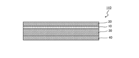
- FIG. 1 is a schematic cross-sectional view of a film for LED backlight according to one embodiment of the present invention.
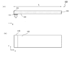
- A is a schematic sectional drawing of the light guide unit by one Embodiment of this invention,
- (b) is a schematic plan view of the light guide unit of (a).
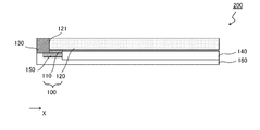
- 1 is a schematic cross-sectional view of an LED backlight according to one embodiment of the present invention.
- FIG. 1 is a schematic cross-sectional view of an LED backlight film according to one embodiment of the present invention.
- the LED backlight film 110 according to this embodiment includes a low refractive index layer 10 and a first pressure-sensitive adhesive layer 20 disposed on at least one side of the low refractive index layer 10.
- the refractive index of the low refractive index layer 10 is 1.25 or less.
- the LED backlight film 110 further includes a substrate 30 as necessary.
- the base material 30 is provided so as to be peelable from the low refractive index layer 10.
- the LED backlight film 110 further includes a second pressure-sensitive adhesive layer 40 as necessary.
- the first pressure-sensitive adhesive layer 20, the low refractive index layer 10, the base material 30, and the second pressure-sensitive adhesive layer 40 are: Arranged in this order.
- each structural member in drawing is modeled, and the size and / or reduced scale are described differently from actual.
- FIG. 2A is a schematic cross-sectional view of a light guide unit according to an embodiment of the present invention
- FIG. 2B is a schematic plan view of the light guide unit of FIG. 2B is a view of the light guide unit 100 of FIG. 2A as viewed from below (the lower side of the drawing).
- the light guide unit 100 includes an LED backlight film 110 and a light guide plate 120.
- the LED backlight film 110 of the present invention can be used by being attached to a part of the main surface of the light guide plate 120.
- the LED backlight film 110 is used by adhering to the vicinity of the light guide direction end face 121 of the light guide plate 120 (the end face 121 where the light source is expected to be arranged).
- the backlight film 110 covers a part of one side of the light guide plate 120 in the light guide direction X, and in a direction Y perpendicular to the light guide direction X in a plane including the light guide direction X.
- the light guide plate 120 may be used by being attached to the light guide plate 120 so as to cover the entire area of one side of the light guide plate 120.
- the LED backlight film 110 may be attached so that the light guide plate 120 and the low refractive index layer 10 are disposed via the first pressure-sensitive adhesive layer 20.
- the LED backlight film 110 is preferably disposed directly on the light guide plate. Further, when the LED backlight film 110 includes the base material 30, the LED backlight film 110 is directly disposed such that the low refractive index layer 10 is on the inner side (light guide plate side) than the base material 30. It is preferable.
- the light guide unit 100 can be applied to a sidelight type planar backlight. For example, the light guide unit 100 can be used by disposing the LED light source 130 on the end surface 121 of the light guide plate 120 and configure the LED backlight 200 together with the LED light source 130 (FIG. 3).
- the light guide direction means a direction perpendicular to an end face on which the light source is planned to be arranged.
- the light guide plate can be fixed to the LED backlight body. Moreover, light can be favorably reflected at the interface between the light guide plate and the LED backlight film, and the light guide efficiency can be improved. By reflecting light well in the vicinity of the incident surface, the emitted light intensity of the entire light guide plate can be increased. Furthermore, if the LED backlight film of the present invention is used as described above, light leakage and brightness unevenness in the vicinity of the incident surface of the light guide plate can be prevented. Furthermore, since the light guide plate can be positioned by adjusting the film thickness of the LED backlight film, the positional relationship between the LED light source and the light guide plate can be easily optimized.
- the thickness of the film for LED backlight is preferably 120 ⁇ m or less, more preferably 110 ⁇ m or less, still more preferably 100 ⁇ m or less, and particularly preferably 60 ⁇ m or less. If it is such a range, when the film for LED backlight is applied to a backlight, the positional relationship of an LED light source and a light-guide plate can be adjusted appropriately.
- the thickness of the LED backlight film may be an appropriate thickness depending on the form of the backlight to which the LED backlight film is applied. The lower limit of the thickness of the LED backlight film is, for example, 10 ⁇ m.
- the heat resistance of the LED backlight film is preferably 60 ° C. or higher, and more preferably 80 ° C. or higher. If it is such a range, the film for LED backlight which can be suitable for the use in the LED light source vicinity and can maintain the said effect favorably can be obtained.
- heat resistance is a change in characteristics before and after charging for 300 hours or longer in an oven at 60 ° C. or 80 ° C. or higher (the amount of emitted light, directivity, and the layer with which the LED backlight film is in direct contact). (Adhesion force) indicates a range that does not affect the use for an LED backlight.
- the refractive index of the low refractive index layer is 1.25 or less. If an LED backlight film having a low refractive index layer having such a refractive index is laminated on a light guide plate, light can be favorably reflected at the interface between the light guide plate and the LED backlight film. An LED backlight having excellent waveguide efficiency and excellent emission intensity can be obtained.
- the refractive index of the low refractive index layer is preferably 1.20 or less, more preferably 1.18 or less, and even more preferably 1.15 or less. The lower the refractive index of the low refractive index layer, the better. However, the lower limit is, for example, 1.07 or more (preferably 1.05 or more). In this specification, the refractive index refers to a refractive index measured at a wavelength of 550 nm.
- the thickness of the low refractive index layer is preferably 0.01 ⁇ m to 100 ⁇ m, more preferably 0.05 ⁇ m to 70 ⁇ m, still more preferably 0.1 ⁇ m to 48 ⁇ m, and particularly preferably 0.3 ⁇ m to 40 ⁇ m. And most preferably from 0.3 ⁇ m to 30 ⁇ m.
- the low refractive index layer may be in any suitable form as long as the refractive index is in the above range.
- the low refractive index layer is configured as a porous body having a predetermined void.
- the porosity of the low refractive index layer configured as a porous body is preferably 5% by volume to 95% by volume, more preferably 15% by volume to 95% by volume, and even more preferably 25% by volume to 90% by volume. More preferably, it is 35 volume% to 90 volume%, particularly preferably 38 volume% to 85 volume%, and most preferably 40 volume% to 80 volume%. Within such a range, a low refractive index layer having a particularly low refractive index can be formed. If the layer whose porosity is to be measured is only a single layer and contains voids, the ratio (volume ratio) between the constituent material of the layer and air can be calculated by a standard method (for example, measuring the weight and volume to calculate the density).
- the porosity (volume%) can be calculated. Further, since there is a correlation between the refractive index and the porosity, for example, the porosity can be calculated from the value of the refractive index of the layer. Specifically, for example, the porosity is calculated from the value of the refractive index measured with an ellipsometer from Lorentz-Lorenz's formula (Lorentz-Lorentz equation).
- the size of the voids is preferably 2 nm to 500 nm, more preferably 5 nm to 500 nm, still more preferably 10 nm to 200 nm, and particularly preferably 20 nm to 100 nm.
- the size of the void can be measured by the BET test method. Specifically, 0.1 g of a low refractive index layer sample was put into a capillary of a specific surface area measuring device (trade name “ASAP2020” manufactured by Micromeritic Co., Ltd.), and then dried under reduced pressure at room temperature for 24 hours. After degassing the gas in the void structure, nitrogen gas is adsorbed on the low refractive index layer sample to obtain a pore distribution, and the void size can be evaluated from the pore distribution.
- a specific surface area measuring device trade name “ASAP2020” manufactured by Micromeritic Co., Ltd.
- the peak pore diameter of the low refractive index layer configured as a porous body is preferably 5 nm to 50 nm, more preferably 10 nm to 40 nm, and still more preferably 20 nm to 30 nm.
- the peak pore diameter is determined from a BJH plot and a BET plot by nitrogen adsorption and an isothermal adsorption line using a pore distribution / specific surface area measuring device (trade name “BELLSORP MINI” manufactured by Microtrack Bell).
- the low refractive index layer configured as a porous body is, for example, silicone particles, silicone particles having fine pores, substantially spherical particles such as silica hollow nanoparticles, fibrous particles such as cellulose nanofibers, alumina nanofibers, silica nanofibers, Including tabular grains such as nanoclay composed of bentonite.
- the low refractive index layer configured as a porous body is a porous body configured by chemically bonding particles to each other.
- at least a part of the particles constituting the low refractive index layer configured as a porous body may be bonded via a small amount of a binder component (for example, a binder component having a particle weight or less).
- the porosity and refractive index of the low refractive index layer configured as a porous body can be adjusted by the particle size, particle size distribution, etc. of the particles constituting the low refractive index layer.
- Examples of a method for obtaining a low refractive index layer configured as a porous body include, for example, JP 2010-189212 A, JP 2008-040171 A, JP 2006-011175 A, and International Publication No. 2004/113966 Pamphlet. And the methods described in those references. Specifically, silica-based compounds; hydrolyzable silanes, a method of hydrolyzing and polycondensing at least one of a partially hydrolyzed product and a dehydrated condensate thereof, porous particles and / or hollow fine particles are used.
- the low refractive index layer is not limited to this manufacturing method, and may be manufactured by any manufacturing method.
- the low refractive index layer is a porous silicone material.
- Silicone porous bodies can be composed of microporous particles of silicon compounds bonded together. Examples of the fine pore particles of the silicon compound include a pulverized product of a gel silicon compound.
- the silicone porous body can be formed, for example, by applying a coating liquid containing a pulverized body of a gel-like silicon compound to a substrate.
- the crushed body of the gel-like silicon compound can be chemically bonded (for example, siloxane bond) by, for example, the action of a catalyst, light irradiation, heating, or the like.
- R 1 is preferably a linear or branched alkyl group having 1 to 6 carbon atoms, more preferably a linear or branched alkyl group having 1 to 4 carbon atoms, and still more preferably a carbon number. 1 or 2 alkyl groups.
- R 2 is preferably a hydrogen atom or a linear or branched alkyl group having 1 to 6 carbon atoms, more preferably a hydrogen atom or a linear or branched alkyl group having 1 to 4 carbon atoms. And more preferably a hydrogen atom or an alkyl group having 1 to 2 carbon atoms.
- silicon compound examples include tris (hydroxy) methylsilane and trimethoxy (methyl) silane.
- the silicon compound is a trifunctional silane. If trifunctional silane is used, a low refractive index layer having a particularly low refractive index can be formed. In another embodiment, the silicon compound is a tetrafunctional silane. If tetrafunctional silane is used, a low refractive index layer having excellent scratch resistance can be formed.
- the gelation of the silicon compound can be performed, for example, by a dehydration condensation reaction of the silicon compound. Any appropriate method can be adopted as the method of the dehydration condensation reaction.
- Arbitrary appropriate methods can be employ
- the pulverization method include a method using a pulverization apparatus using a cavitation phenomenon such as an ultrasonic homogenizer and a high-speed rotation homogenizer.
- the volume average particle diameter of the fine pore particles of the silicon compound is preferably 0.1 ⁇ m to 2 ⁇ m, more preferably 0.2 ⁇ m to 1.5 ⁇ m, and still more preferably 0.2 ⁇ m. 4 ⁇ m to 1 ⁇ m.
- the volume average particle diameter can be measured by a dynamic light scattering method.
- the ratio of the particles having a particle size of 0.4 ⁇ m to 1 ⁇ m to the total amount of the particles is 50% by weight to 99.9% by weight. Preferably, it is 80 to 99.8% by weight, more preferably 90 to 99.7% by weight.
- the ratio of particles having a particle size of 1 ⁇ m to 2 ⁇ m to the total amount of particles is preferably 0.1% by weight to 50% by weight, more preferably 0.2% by weight to 20% by weight, More preferably, it is from 10% by weight to 10% by weight.
- the particle size distribution can be measured by a particle size distribution evaluation apparatus.
- the substrate can be formed of any suitable material.
- suitable material examples include thermoplastic resins such as polyethylene terephthalate resin, acrylic resin, cellulose resin, cycloolefin resin, and olefin resin; thermosetting resins; inorganic materials such as glass and silicon Carbon fiber materials and the like.
- the thickness of the substrate is not particularly limited, and can be set to any appropriate thickness depending on the application.
- the thickness of the substrate is, for example, 1 ⁇ m to 100 ⁇ m, preferably 1 ⁇ m to 60 ⁇ m, and more preferably 2 ⁇ m to 40 ⁇ m.
- the substrate may be transparent or opaque. In one embodiment, the substrate is transparent. When the substrate is transparent, its transmittance is preferably 50% to 99%, more preferably 60% to 99%, and even more preferably 70% to 99%. If it is such a range, even if it is a case where the light omission to a base material arises, the film for LED backlight which can implement
- the 1st adhesive layer contains arbitrary appropriate adhesives.
- the pressure-sensitive adhesive preferably has transparency and optical isotropy.
- Specific examples of the pressure-sensitive adhesive include rubber-based pressure-sensitive adhesives, acrylic pressure-sensitive adhesives, silicone-based pressure-sensitive adhesives, epoxy-based pressure-sensitive adhesives, and cellulose-based pressure-sensitive adhesives.
- it is a rubber adhesive or an acrylic adhesive.
- an acrylic adhesive is used as the adhesive.
- the acrylic pressure-sensitive adhesive include an acrylic pressure-sensitive adhesive having an acrylic polymer (homopolymer or copolymer) containing a structural unit derived from alkyl (meth) acrylate as a base polymer.
- the alkyl group of the alkyl (meth) acrylate has, for example, 2 to 18 carbon atoms.
- the alkyl group may be linear or branched.
- the number of carbon atoms of the alkyl group is preferably 2 to 14, more preferably 3 to 12, and further preferably 4 to 9.
- Specific examples of the alkyl (meth) acrylate include ethyl (meth) acrylate, n-butyl (meth) acrylate, s-butyl (meth) acrylate, t-butyl (meth) acrylate, isobutyl (meth) acrylate, and n-pentyl.
- (Meth) acrylate isopentyl (meth) acrylate, hexyl (meth) acrylate, heptyl (meth) acrylate, isoamyl (meth) acrylate, 2-ethylhexyl (meth) acrylate, n-octyl (meth) acrylate, isooctyl (meth) Acrylate, n-nonyl (meth) acrylate, isononyl (meth) acrylate, n-decyl (meth) acrylate, isodecyl (meth) acrylate, n-dodecyl (meth) acrylate, isomyristyl (meth) acrylate n- tridecyl (meth) acrylate, n- tetradecyl (meth) acrylate, stearyl (meth) acrylate, isostearyl (meth) acrylate.
- the content of the constituent unit derived from alkyl (meth) acrylate is preferably 30 parts by weight to 100 parts by weight, more preferably 85 parts by weight to 99.99 parts by weight with respect to 100 parts by weight of the acrylic polymer. More preferably, it is 90 parts by weight to 99.95 parts by weight, and particularly preferably 95 parts by weight to 99 parts by weight. If it is such a range, the adhesive layer which is excellent in adhesiveness can be formed.
- the acrylic polymer further includes a structural unit derived from a functional group-containing monomer.
- a functional group-containing monomer a monomer having any appropriate functional group may be used.
- Specific examples of the functional group-containing monomer include a carboxyl group-containing monomer, a hydroxyl group-containing monomer, an amide group-containing monomer, and an amino group-containing monomer. If these monomers are used, an adhesive layer having excellent heat resistance can be formed.
- a functional group containing monomer may be used independently and may be used in combination of 2 or more type.
- carboxyl group-containing monomer a polymerizable functional group having an unsaturated double bond such as a (meth) acryloyl group or a vinyl group, and a monomer having a carboxyl group can be used.
- the carboxyl group-containing monomer include (meth) acrylic acid, carboxyethyl (meth) acrylate, carboxypentyl (meth) acrylate, itaconic acid, maleic acid, fumaric acid, and crotonic acid. Of these, (meth) acrylic acid is preferable, and acrylic acid is particularly preferable.
- hydroxyl group-containing monomer a polymerizable functional group having an unsaturated double bond such as a (meth) acryloyl group or a vinyl group, and a monomer having a hydroxyl group can be used.
- the hydroxyl group-containing monomer include 2-hydroxyethyl (meth) acrylate, 2-hydroxybutyl (meth) acrylate, 3-hydroxypropyl (meth) acrylate, 4-hydroxybutyl (meth) acrylate, 6-hydroxyhexyl ( Hydroxyalkyl (meth) acrylates such as (meth) acrylate, 8-hydroxyoctyl (meth) acrylate, 10-hydroxydecyl (meth) acrylate, 12-hydroxylauryl (meth) acrylate; hydroxyethyl (meth) acrylamide, N-methylol ( (Meth) acrylamide, others, (4-hydroxymethylcyclohexyl) methyl acrylate, N-methylol (meth)
- amide group-containing monomer a polymerizable functional group having an unsaturated double bond such as a (meth) acryloyl group or a vinyl group, and a monomer having an amide bond can be used.
- amide group-containing monomers include (meth) acrylamide, N, N-dimethyl (meth) acrylamide, N, N-diethyl (meth) acrylamide, N, N-diethylmethacrylamide, N-isopropyl (meth) acrylamide, N-substituted amide monomers such as N-methoxymethyl (meth) acrylamide, N-butoxymethyl (meth) acrylamide N-vinylcaprolactam, N-acryloylmorpholine, N-acryloylpiperidine, N-methacryloylpiperidine, N-acryloylpyrrolidine, Examples include diacetone (meth) acrylamide and N-vinylacetamide.
- amino group-containing monomer a monomer having a (meth) acryloyl group and an amino group can be used.
- amino group-containing monomer a monomer having a tertiary amino group is preferable.
- the tertiary amino group is preferably a tertiary aminoalkyl group.
- examples of the tertiary amino group-containing monomer include N, N-dialkylaminoalkyl (meth) acrylamide and N, N-dialkylaminoalkyl (meth) acrylate.
- tertiary amino group-containing monomer examples include N, N-dimethylaminoethyl (meth) acrylamide, N, N-dimethylaminopropyl (meth) acrylamide, N, N-diethylaminoethyl (meth) acrylamide, N, N-diethylaminopropyl (meth) acrylamide, N, N-dimethylaminoethyl (meth) acrylate, N, N-dimethylaminopropyl (meth) acrylate, N, N-diethylaminoethyl (meth) acrylate, N, N- Examples include diethylaminopropyl (meth) acrylamide.
- Examples of the monomer having a secondary amino group examples include t-butylaminoethyl (meth) acrylate.
- the content of the structural unit derived from the functional group-containing monomer is preferably 0.01 to 15 parts by weight, more preferably 0.05 to 10 parts by weight with respect to 100 parts by weight of the (meth) acrylic polymer. Parts by weight.
- the acrylic polymer may have a structural unit derived from any appropriate other monomer as necessary.
- Other monomers include phenoxyethyl (meth) acrylate, benzyl (meth) acrylate, phenol ethylene oxide modified (meth) acrylate, 2-naphthoethyl (meth) acrylate, 2- (4-methoxy-1-naphthoxy) ethyl (meth) )
- Aromatic ring-containing monomers such as acrylate, phenoxypropyl (meth) acrylate, phenoxydiethylene glycol (meth) acrylate, polystyryl (meth) acrylate, styrene; vinyl ester monomers such as vinyl acetate and vinyl propionate;
- (meth) acrylic acid examples include (meth) acrylic acid alkoxyalkyl monomers such as methoxyethyl and ethoxyethyl (meth) acrylate. The content ratio of the structural units
- the weight average of the acrylic polymer is preferably 1 million to 3 million, more preferably 1.5 to 2.5 million, and further preferably 1.7 to 2.5 million. If it is such a range, the adhesive layer which is excellent in heat resistance and adhesive force can be obtained.
- the weight average molecular weight is a value measured by GPC (gel permeation chromatography) and calculated in terms of polystyrene.
- the pressure-sensitive adhesive may further contain any appropriate additive as required.
- additives include cross-linking agents, pigments, dyes, surfactants, plasticizers, tackifiers, surface lubricants, leveling agents, softeners, antioxidants, anti-aging agents, light stabilizers, and UV absorbers.
- the crosslinking agent include an isocyanate crosslinking agent, an epoxy crosslinking agent, a peroxide crosslinking agent, a metal chelate crosslinking agent, and an oxazoline crosslinking agent. Of these, an isocyanate-based crosslinking agent is preferable.
- the content of the crosslinking agent is preferably 2 parts by weight or less, more preferably 1.5 parts by weight or less, and further preferably 1 part by weight or less with respect to 100 parts by weight of the acrylic polymer.
- the thickness of the first pressure-sensitive adhesive layer is preferably 0.1 ⁇ m to 100 ⁇ m, more preferably 5 ⁇ m to 50 ⁇ m, and further preferably 5 ⁇ m to 25 ⁇ m.
- the refractive index of the first pressure-sensitive adhesive layer is 1.42 to 1.60, more preferably 1.47 to 1.58. If it is such a range, the LED backlight which is excellent in the waveguide efficiency and excellent in the emission intensity can be obtained.
- the light transmittance of the first pressure-sensitive adhesive layer is preferably 85% to 99%, more preferably 88% to 99%, and further preferably 90% to 99%. Further, the haze value of the first pressure-sensitive adhesive layer is preferably 5 or less, more preferably 3 or less, and further preferably 1 or less.
- the first pressure-sensitive adhesive layer is preferably adhered to the light guide plate side in the light guide unit and the LED backlight. In one embodiment, it adheres directly to the light guide plate or indirectly through a resin layer laminated directly on the light guide plate.
- the adhesive force of the first pressure-sensitive adhesive layer with respect to the layer adjacent to the side opposite to the low refractive index layer of the first pressure-sensitive adhesive layer is preferably 0.8 N / 25 mm or more. More preferably, it is 1 N / 25mm or more, More preferably, it is 1.5 N / 25mm or more. The upper limit of the adhesive force is, for example, 30 N / 25 mm.
- the adhesive strength was measured by a method according to JIS Z 0237: 2000 (bonding condition: 2 kg roller 1 reciprocation, peeling speed: 300 mm / min, peeling angle 180 °) in an environment of 23 ° C. Refers to adhesive strength.
- the 2nd adhesive layer contains arbitrary appropriate adhesives.
- the pressure-sensitive adhesive preferably has transparency and optical isotropy.
- Specific examples of the pressure-sensitive adhesive include rubber-based pressure-sensitive adhesives, acrylic pressure-sensitive adhesives, silicone-based pressure-sensitive adhesives, epoxy-based pressure-sensitive adhesives, and cellulose-based pressure-sensitive adhesives.
- it is a rubber adhesive or an acrylic adhesive.
- the acrylic pressure-sensitive adhesive described in the section A-4 may be used.
- the thickness of the second pressure-sensitive adhesive layer is preferably 0.1 ⁇ m to 100 ⁇ m, more preferably 5 ⁇ m to 50 ⁇ m, and further preferably 5 ⁇ m to 25 ⁇ m.
- the second pressure-sensitive adhesive layer is bonded to a flexible substrate (FPC) in the light guide unit and the LED backlight. In one embodiment, it is in intimate contact with the FPC directly or via a resin layer or insulating layer directly laminated on the FPC.
- the adhesive force of the second pressure-sensitive adhesive layer with respect to the layer adjacent to the side opposite to the low refractive index layer of the second pressure-sensitive adhesive layer is preferably 0.5 N / 25 mm or more. More preferably, it is 0.7 N / 25mm or more, More preferably, it is 1.0 N / 25mm or more. The upper limit of the adhesive force is, for example, 30 N / 25 mm.
- the second pressure-sensitive adhesive layer may be transparent or opaque. In one embodiment, the second pressure-sensitive adhesive layer is transparent.
- the transmittance is preferably 50% to 99%, more preferably 60% to 99%, and further preferably 70% to 99%. If it is such a range, even if it is a case where light leakage arises exceeding a low refractive index layer, the film for LED backlight which can implement
- the LED backlight film can be manufactured by any appropriate method. For example, by applying a coating solution for forming a low refractive index layer containing predetermined particles (for example, fine pore particles of the above-mentioned silicon compound, preferably a pulverized body of a gel-like silicon compound) on the base material, and drying it.
- a coating solution for forming a low refractive index layer containing predetermined particles for example, fine pore particles of the above-mentioned silicon compound, preferably a pulverized body of a gel-like silicon compound
- the low refractive index layer forming coating solution contains any appropriate solvent.
- the solvent include isopropyl alcohol, ethanol, methanol, n-butanol, 2-butanol, isobutyl alcohol, pentanol and the like.
- the low refractive index layer forming coating solution further contains a catalyst.
- a catalyst capable of promoting chemical bonding of particles is used.
- the catalyst include base catalysts such as potassium hydroxide, sodium hydroxide and ammonium hydroxide, and acid catalysts such as hydrochloric acid, acetic acid and oxalic acid. Of these, a base catalyst is preferable.
- the content of the catalyst is preferably 0.01 parts by weight to 20 parts by weight, more preferably 0.1 parts by weight to 5 parts by weight with respect to 100 parts by weight of the particles in the coating solution for forming a low refractive index layer. Part.
- any appropriate method can be adopted as a method for applying the coating liquid for forming a low refractive index layer.
- the coating method include bar coater coating, air knife coating, gravure coating, gravure reverse coating, reverse roll coating, lip coating, die coating, and dip coating.
- drying method of the coating liquid for forming the low refractive index layer Any appropriate method can be adopted as a drying method of the coating liquid for forming the low refractive index layer.
- the drying method of the coating liquid may be natural drying, heat drying, or vacuum drying.
- a heating means a hot air fan, a heating roll, a far-infrared heater, etc. are mentioned, for example.
- the coating layer may be subjected to heat treatment.
- heat treatment bonding between particles constituting the low refractive index layer can be promoted.
- the heating temperature is preferably 200 ° C. or higher.
- the said drying process may serve as heat processing.
- the first pressure-sensitive adhesive layer and the second pressure-sensitive adhesive layer can be formed by any appropriate method.
- the first pressure-sensitive adhesive layer and the second pressure-sensitive adhesive are applied by applying a pressure-sensitive adhesive by a method such as bar coater coating, air knife coating, gravure coating, gravure reverse coating, reverse roll coating, lip coating, die coating, or dip coating.
- An agent layer can be formed.
- the first pressure-sensitive adhesive layer and the second pressure-sensitive adhesive layer may be formed by a method of transferring the pressure-sensitive adhesive layer formed on the release liner.
- the irradiation amount of the electron beam is preferably 2 kGy to 100 kGy, more preferably 2 kGy to 70 kGy, and further preferably 5 to 50 kGy.
- the light guide unit of the present invention includes an LED backlight film 110 and a light guide plate 120 as shown in FIGS. 2 (a) and 2 (b).
- the LED backlight film 110 is laminated and disposed on a part of one side of the light guide plate 120. More specifically, the LED backlight film 110 is adhered and disposed in the vicinity of the light guide direction end surface 121 of the light guide plate 120 (the end surface 121 where the light source is planned to be disposed).
- the backlight film 110 covers a part of one surface 122 of the light guide plate 120 in the light guide direction X of the light guide plate 120 and is perpendicular to the light guide direction X in a plane including the light guide direction X.
- the light guide plate 120 can be attached to the light guide plate 120 so as to cover the entire area of one side 122 of the light guide plate 120.
- the LED backlight film 110 can be attached so that the light guide plate and the low refractive index layer are disposed via the first pressure-sensitive adhesive layer.
- the LED backlight film 110 is preferably disposed directly on the light guide plate.
- the LED backlight film 110 includes a base material, the LED backlight film 110 is preferably arranged directly such that the low refractive index layer is on the inner side (light guide plate side) than the base material. .
- directly disposed means that the LED backlight film 110 and the light guide plate 120 are disposed such that no other layer is disposed between the LED backlight film 110 and the light guide plate 120. Means.
- the surface of the light guide plate to which the LED backlight film is attached corresponds to the surface opposite to the light exit surface when the light guide unit is applied to the LED backlight.
- the LED backlight film may be disposed such that one end thereof is in contact with the end surface of the light guide plate, or may be disposed at a slight distance from the end surface of the light guide plate.
- the distance of the LED backlight film from the light guide plate is preferably 5 mm or less, more preferably 3 mm or less, particularly Preferably it is 1 mm or less.
- the length Lx in the light guide direction of the LED backlight film is preferably 10 mm or less, more preferably 8 mm or less, still more preferably 5 mm or less, and particularly preferably 3 mm or less.
- the lower limit of the length Lx is, for example, 0.5 mm.
- the ratio (Lx / L) of the length Lx in the light guide direction of the LED backlight film to the length L in the light guide direction of the light guide plate is preferably 1/3000 to 1/10, more preferably 1/1000 to 1/20.
- the light intensity of the entire light guide plate can be increased by reflecting light well in the vicinity of the incident surface.
- the LED backlight film can be applied to a region where light is not emitted from the light guide plate.
- the extremely narrow size LED backlight film it is possible to increase the emitted light intensity of the entire light guide plate, and to improve the waveguide efficiency by the member applied to the region where the light emission is not performed. This is the result of the present invention.
- any appropriate material can be used as long as it can efficiently guide the light emitted from the LED light source.
- the material constituting the light guide plate include acrylic resins, polycarbonate resins, and cycloolefin resins.
- the thickness of the light guide plate is, for example, 100 ⁇ m to 2000 ⁇ m.
- the refractive index of the light guide plate is preferably 1.4 or more, more preferably greater than 1.45, even more preferably greater than 1.45 and 2 or less, and particularly preferably 1.48 to 1.8. .
- the difference between the refractive index of the light guide plate and the refractive index layer of the low refractive index layer is preferably 0.2 or more, more preferably 0.23 or more, and further preferably 0.25 or more. Within such a range, light can be favorably reflected at the interface between the light guide plate and the LED backlight film, and an LED backlight unit having excellent light guiding efficiency and excellent emission intensity can be obtained. it can.
- the refractive index of the light guide plate is higher than the refractive index of the low refractive index layer.
- FIG. 3 is a schematic cross-sectional view of an LED backlight according to one embodiment of the present invention.
- the LED backlight 200 may include the light source unit 100 and the LED light source 130 disposed on the end surface 121 on the side where the LED backlight film 110 of the light guide plate 120 included in the light guide unit 100 is disposed.
- the thickness of the LED backlight film is preferably (LED light source thickness-light guide plate thickness) or less. More specifically, the thickness of the film for the LED backlight is ⁇ (LED light source thickness ⁇ light guide plate thickness) ⁇ 10% ⁇ to ⁇ (LED light source thickness ⁇ light guide plate thickness) ⁇ 100% ⁇ . It is more preferable that ⁇ (LED light source thickness ⁇ light guide plate thickness) ⁇ 30% ⁇ to ⁇ (LED light source thickness ⁇ light guide plate thickness) ⁇ 100% ⁇ , ⁇ (LED light source thickness ⁇ The thickness of the light guide plate) ⁇ 50% ⁇ to ⁇ (LED light source thickness ⁇ light guide plate thickness) ⁇ 100% ⁇ is more preferable. If it is such a range, in a backlight unit provided with an LED light source, the positional relationship of an LED light source and a light-guide plate can be adjusted appropriately.
- the thickness of the LED light source is usually 200 ⁇ m to 5000 ⁇ m.
- the LED backlight may further include any appropriate other member.
- the LED backlight 200 may further include a reflecting plate 140 provided via an air layer on the surface of the light guide plate 120 where the LED backlight film 110 is not disposed.
- the flexible substrate 150 for LED may be arrange
- the LED flexible substrate may be provided with a colored layer (for example, a white ink layer) on the surface of the LED backlight film side.
- the LED backlight 200 may include a housing 160 that houses the above-described members.
- ⁇ Evaluation method> (1) Refractive index The refractive index layer was cut into a size of 50 mm x 50 mm, and this was bonded to the surface of a glass plate (thickness: 3 mm) via an adhesive layer. The center of the back surface of the glass plate (diameter of about 20 mm) was painted with black magic to make a sample that did not reflect on the back surface of the glass plate. The above sample was set in an ellipsometer (JA Woollam Japan: VASE), and the refractive index was measured under the conditions of a wavelength of 500 nm and an incident angle of 50 to 80 degrees.
- the LED backlight films obtained in Examples and Comparative Examples are used as LED backlights (light guide plate refractive index: 1.49, LED light source thickness: 300 ⁇ m).
- the brightness unevenness of the light guide plate exit surface when the LED light source was turned on was confirmed visually.
- the case where it was able to illuminate uniformly was set to pass (in Table 1, ⁇ ), and the case where brightness unevenness and light leakage could be confirmed was set to fail (in Table 1, x).
- the gelled silicon compound in the mixed solution D was pulverized (high-pressure medialess pulverization).
- a homogenizer (trade name “UH-50” manufactured by SMT Co., Ltd.) is used, and 1.85 g of gel compound and IBA in the mixed solution D ′ are added to a 5 cc screw bottle. After weighing 15 g, grinding was performed for 2 minutes under conditions of 50 W and 20 kHz.
- the gel silicon compound in the mixed solution D was pulverized, so that the mixed solution D ′ became a sol solution of a pulverized product.
- the volume average particle size indicating the particle size variation of the pulverized product contained in the mixed solution D ′ was confirmed with a dynamic light scattering nanotrack particle size analyzer (manufactured by Nikkiso Co., Ltd., UPA-EX150 type), 0.50 to It was 0.70.
- the acrylic pressure-sensitive adhesive solution is applied to one side of a silicone-treated polyethylene terephthalate (PET) film (Mitsubishi Chemical Polyester Film Co., Ltd., thickness: 38 ⁇ m), and the thickness of the pressure-sensitive adhesive layer after drying is 10 ⁇ m. Then, it was dried at 150 ° C. for 3 minutes to form a first pressure-sensitive adhesive layer.
- PET polyethylene terephthalate
- an isocyanate cross-linking agent coronate L manufactured by Nippon Polyurethane Industry Co., Ltd., adduct of tolylene diisocyanate of trimethylolpropane
- benzoyl peroxide Japan
- An acrylic pressure-sensitive adhesive solution was prepared by blending 0.2 parts of Nyper BMT manufactured by Yushi Co., Ltd. and 0.2 part of ⁇ -glycidoxypropylmethoxysilane (manufactured by Shin-Etsu Chemical Co., Ltd .: KBM-403).
- the acrylic pressure-sensitive adhesive solution is applied on one side of a silicone-treated polyethylene terephthalate (PET) film (Mitsubishi Chemical Polyester Film Co., Ltd., thickness: 38 ⁇ m), and the pressure-sensitive adhesive layer after drying has a thickness of 15 ⁇ m. And then dried at 150 ° C. for 3 minutes to form a second pressure-sensitive adhesive layer.
- PET polyethylene terephthalate
- Example 1 The low refractive index layer coating solution prepared in Production Example 1 is applied to an acrylic resin film (thickness: 20 ⁇ m) as a substrate, dried, and a low refractive index layer (850 nm thick on one side of the substrate ( A laminate having a refractive index of 1.18) was obtained. After irradiating UV (300 mJ) to the low refractive index layer, the pressure-sensitive adhesive layer (first pressure-sensitive adhesive layer) of Production Example 2 is placed on the low refractive index layer side, and the pressure-sensitive adhesive layer of Production Example 3 (second pressure-sensitive adhesive) Layer) to each substrate side and aged at 60 ° C.
- an LED backlight capable of efficiently guiding incident light can be obtained by using the film for LED backlight of the present invention.
Landscapes
- Physics & Mathematics (AREA)
- Optics & Photonics (AREA)
- Engineering & Computer Science (AREA)
- General Physics & Mathematics (AREA)
- Microelectronics & Electronic Packaging (AREA)
- General Engineering & Computer Science (AREA)
- Planar Illumination Modules (AREA)
Abstract
Priority Applications (5)
| Application Number | Priority Date | Filing Date | Title |
|---|---|---|---|
| JP2019569043A JPWO2019151073A1 (ja) | 2018-02-02 | 2019-01-23 | Ledバックライト用フィルム、ledバックライト |
| KR1020207021709A KR20200118009A (ko) | 2018-02-02 | 2019-01-23 | Led 백라이트용 필름, led 백라이트 |
| CN201980010198.2A CN111656087A (zh) | 2018-02-02 | 2019-01-23 | Led背光源用膜、led背光源 |
| EP19748048.6A EP3748221A4 (fr) | 2018-02-02 | 2019-01-23 | Film de rétroéclairage à del et rétroéclairage à del |
| US16/937,131 US20200355866A1 (en) | 2018-02-02 | 2020-07-23 | Led backlight film and led backlight |
Applications Claiming Priority (2)
| Application Number | Priority Date | Filing Date | Title |
|---|---|---|---|
| JP2018-017206 | 2018-02-02 | ||
| JP2018017206 | 2018-02-02 |
Related Child Applications (1)
| Application Number | Title | Priority Date | Filing Date |
|---|---|---|---|
| US16/937,131 Continuation-In-Part US20200355866A1 (en) | 2018-02-02 | 2020-07-23 | Led backlight film and led backlight |
Publications (1)
| Publication Number | Publication Date |
|---|---|
| WO2019151073A1 true WO2019151073A1 (fr) | 2019-08-08 |
Family
ID=67478722
Family Applications (1)
| Application Number | Title | Priority Date | Filing Date |
|---|---|---|---|
| PCT/JP2019/002036 Ceased WO2019151073A1 (fr) | 2018-02-02 | 2019-01-23 | Film de rétroéclairage à del et rétroéclairage à del |
Country Status (7)
| Country | Link |
|---|---|
| US (1) | US20200355866A1 (fr) |
| EP (1) | EP3748221A4 (fr) |
| JP (2) | JPWO2019151073A1 (fr) |
| KR (1) | KR20200118009A (fr) |
| CN (1) | CN111656087A (fr) |
| TW (1) | TWI846684B (fr) |
| WO (1) | WO2019151073A1 (fr) |
Cited By (12)
| Publication number | Priority date | Publication date | Assignee | Title |
|---|---|---|---|---|
| WO2021193896A1 (fr) | 2020-03-27 | 2021-09-30 | 日東電工株式会社 | Unité de rétroéclairage et dispositif d'affichage d'image |
| WO2021193591A1 (fr) | 2020-03-24 | 2021-09-30 | 日東電工株式会社 | Stratifié optique à couche adhésive double face, et dispositif optique |
| WO2021193894A1 (fr) * | 2020-03-27 | 2021-09-30 | 日東電工株式会社 | Dispositif d'éclairage |
| WO2021193895A1 (fr) | 2020-03-27 | 2021-09-30 | 日東電工株式会社 | Élément optique et unité de rétro-éclairage utilisant ledit élément optique, et dispositif d'affichage d'images |
| WO2021193789A1 (fr) | 2020-03-26 | 2021-09-30 | 日東電工株式会社 | Élément optique, et unité de rétroéclairage et dispositif d'affichage d'image à l'aide dudit élément optique |
| WO2021200770A1 (fr) | 2020-03-30 | 2021-10-07 | 日東電工株式会社 | Unité de rétroéclairage et dispositif d'affichage d'image |
| WO2023162528A1 (fr) | 2022-02-28 | 2023-08-31 | 日東電工株式会社 | Film multicouche |
| WO2023163185A1 (fr) | 2022-02-28 | 2023-08-31 | 日東電工株式会社 | Élément optique et lunettes ar et visiocasque utilisant ledit élément optique |
| WO2023181709A1 (fr) | 2022-03-25 | 2023-09-28 | 日東電工株式会社 | Corps stratifié optique |
| WO2023189089A1 (fr) | 2022-03-31 | 2023-10-05 | 日東電工株式会社 | Corps multicouche optique et procédé de production de corps multicouche optique |
| WO2024202547A1 (fr) | 2023-03-31 | 2024-10-03 | 日東電工株式会社 | Stratifié et procédé de fabrication de stratifié |
| WO2025069519A1 (fr) | 2023-09-29 | 2025-04-03 | 日東電工株式会社 | Stratifié |
Families Citing this family (3)
| Publication number | Priority date | Publication date | Assignee | Title |
|---|---|---|---|---|
| WO2022265050A1 (fr) | 2021-06-18 | 2022-12-22 | ローム株式会社 | Transducteur et dispositif électronique |
| CN115175387B (zh) * | 2022-07-15 | 2025-09-16 | 上海骏珲新材料科技有限公司 | 自限温远红外碳纤维复合面状电热材料及其制备方法 |
| DE102022130344A1 (de) * | 2022-11-16 | 2024-05-16 | Webasto SE | Fahrzeugscheibe mit einem Verbundaufbau |
Citations (9)
| Publication number | Priority date | Publication date | Assignee | Title |
|---|---|---|---|---|
| JPH09145903A (ja) * | 1995-11-27 | 1997-06-06 | Dainippon Printing Co Ltd | 反射防止フィルム |
| WO2004113966A1 (fr) | 2003-06-18 | 2004-12-29 | Asahi Kasei Kabushiki Kaisha | Film antireflet |
| JP2006011175A (ja) | 2004-06-28 | 2006-01-12 | Pentax Corp | 反射防止膜を有する光学素子及びその製造方法 |
| JP2008040171A (ja) | 2006-08-07 | 2008-02-21 | Pentax Corp | セルフクリーニング効果を有する反射防止膜を設けた光学素子及びその製造方法 |
| JP2010189212A (ja) | 2009-02-17 | 2010-09-02 | Shinshu Univ | 多孔質シリカ膜およびその製造方法 |
| JP2011207751A (ja) * | 2010-03-11 | 2011-10-20 | Mitsubishi Chemicals Corp | シリカ系多孔質膜の製造方法 |
| JP2012059645A (ja) * | 2010-09-10 | 2012-03-22 | Fujikura Ltd | 面状発光装置および照明モジュール |
| JP2012114284A (ja) | 2010-11-25 | 2012-06-14 | Toshiba Corp | Ledモジュール及び照明装置 |
| JP2017047677A (ja) | 2015-07-31 | 2017-03-09 | 日東電工株式会社 | 光学積層体、光学積層体の製造方法、光学部材、画像表示装置、光学部材の製造方法および画像表示装置の製造方法 |
Family Cites Families (12)
| Publication number | Priority date | Publication date | Assignee | Title |
|---|---|---|---|---|
| JPH03261988A (ja) * | 1990-03-12 | 1991-11-21 | Sumitomo Chem Co Ltd | 面状発光体 |
| US20070264447A1 (en) * | 2004-08-30 | 2007-11-15 | Teijin Dupont Films Japan Limited | Optical Film Laminated Body |
| KR20120115568A (ko) * | 2010-02-10 | 2012-10-18 | 쓰리엠 이노베이티브 프로퍼티즈 컴파니 | 점탄성 층을 구비한 조명 장치 |
| JP6356420B2 (ja) * | 2010-04-14 | 2018-07-11 | スリーエム イノベイティブ プロパティズ カンパニー | パターン付き勾配ポリマーフィルム及び方法 |
| TWI534458B (zh) * | 2010-10-20 | 2016-05-21 | 3M新設資產公司 | 經保護之低折射率光學元件 |
| KR20130028270A (ko) * | 2011-09-09 | 2013-03-19 | 엘지디스플레이 주식회사 | 반사 시트 및 그의 제조방법, 반사 시트를 포함하는 액정표시장치 |
| KR102064751B1 (ko) * | 2014-02-27 | 2020-01-10 | 엘지디스플레이 주식회사 | 베젤이 최소화된 액정표시소자 |
| EP3187927B1 (fr) * | 2014-08-28 | 2022-06-29 | Sony Group Corporation | Dispositif d'affichage et dispositif d'éclairage |
| JP2017064954A (ja) * | 2015-09-28 | 2017-04-06 | 日東電工株式会社 | 積層フィルムの製造方法および画像表示装置の製造方法 |
| JP6966850B2 (ja) * | 2016-03-18 | 2021-11-17 | 日東電工株式会社 | 光学部材、ならびに、該光学部材を用いたバックライトユニットおよび液晶表示装置 |
| JP6809824B2 (ja) * | 2016-07-04 | 2021-01-06 | 日東電工株式会社 | 光学積層体の製造方法、および光学積層体中間体 |
| TWI587052B (zh) * | 2016-07-18 | 2017-06-11 | 恆顥科技股份有限公司 | 光源模組及顯示裝置 |
-
2019
- 2019-01-23 KR KR1020207021709A patent/KR20200118009A/ko not_active Ceased
- 2019-01-23 JP JP2019569043A patent/JPWO2019151073A1/ja active Pending
- 2019-01-23 EP EP19748048.6A patent/EP3748221A4/fr active Pending
- 2019-01-23 WO PCT/JP2019/002036 patent/WO2019151073A1/fr not_active Ceased
- 2019-01-23 CN CN201980010198.2A patent/CN111656087A/zh active Pending
- 2019-01-25 TW TW108102907A patent/TWI846684B/zh active
-
2020
- 2020-07-23 US US16/937,131 patent/US20200355866A1/en not_active Abandoned
-
2021
- 2021-04-09 JP JP2021066529A patent/JP7181961B2/ja active Active
Patent Citations (9)
| Publication number | Priority date | Publication date | Assignee | Title |
|---|---|---|---|---|
| JPH09145903A (ja) * | 1995-11-27 | 1997-06-06 | Dainippon Printing Co Ltd | 反射防止フィルム |
| WO2004113966A1 (fr) | 2003-06-18 | 2004-12-29 | Asahi Kasei Kabushiki Kaisha | Film antireflet |
| JP2006011175A (ja) | 2004-06-28 | 2006-01-12 | Pentax Corp | 反射防止膜を有する光学素子及びその製造方法 |
| JP2008040171A (ja) | 2006-08-07 | 2008-02-21 | Pentax Corp | セルフクリーニング効果を有する反射防止膜を設けた光学素子及びその製造方法 |
| JP2010189212A (ja) | 2009-02-17 | 2010-09-02 | Shinshu Univ | 多孔質シリカ膜およびその製造方法 |
| JP2011207751A (ja) * | 2010-03-11 | 2011-10-20 | Mitsubishi Chemicals Corp | シリカ系多孔質膜の製造方法 |
| JP2012059645A (ja) * | 2010-09-10 | 2012-03-22 | Fujikura Ltd | 面状発光装置および照明モジュール |
| JP2012114284A (ja) | 2010-11-25 | 2012-06-14 | Toshiba Corp | Ledモジュール及び照明装置 |
| JP2017047677A (ja) | 2015-07-31 | 2017-03-09 | 日東電工株式会社 | 光学積層体、光学積層体の製造方法、光学部材、画像表示装置、光学部材の製造方法および画像表示装置の製造方法 |
Non-Patent Citations (1)
| Title |
|---|
| See also references of EP3748221A4 |
Cited By (21)
| Publication number | Priority date | Publication date | Assignee | Title |
|---|---|---|---|---|
| WO2021193591A1 (fr) | 2020-03-24 | 2021-09-30 | 日東電工株式会社 | Stratifié optique à couche adhésive double face, et dispositif optique |
| WO2021193789A1 (fr) | 2020-03-26 | 2021-09-30 | 日東電工株式会社 | Élément optique, et unité de rétroéclairage et dispositif d'affichage d'image à l'aide dudit élément optique |
| US11994709B2 (en) | 2020-03-26 | 2024-05-28 | Nitto Denko Corporation | Optical member, and backlight unit and image display device using said optical member |
| EP4130561A4 (fr) * | 2020-03-26 | 2024-03-20 | Nitto Denko Corporation | Élément optique, et unité de rétroéclairage et dispositif d'affichage d'image à l'aide dudit élément optique |
| EP4130546A4 (fr) * | 2020-03-27 | 2024-04-03 | Nitto Denko Corporation | Dispositif d'éclairage |
| US12044880B2 (en) | 2020-03-27 | 2024-07-23 | Nitto Denko Corporation | Backlight unit and image display device |
| JPWO2021193894A1 (fr) * | 2020-03-27 | 2021-09-30 | ||
| KR20220158708A (ko) | 2020-03-27 | 2022-12-01 | 닛토덴코 가부시키가이샤 | 백라이트 유닛 및 화상 표시 장치 |
| WO2021193894A1 (fr) * | 2020-03-27 | 2021-09-30 | 日東電工株式会社 | Dispositif d'éclairage |
| WO2021193896A1 (fr) | 2020-03-27 | 2021-09-30 | 日東電工株式会社 | Unité de rétroéclairage et dispositif d'affichage d'image |
| WO2021193895A1 (fr) | 2020-03-27 | 2021-09-30 | 日東電工株式会社 | Élément optique et unité de rétro-éclairage utilisant ledit élément optique, et dispositif d'affichage d'images |
| US11921311B2 (en) | 2020-03-27 | 2024-03-05 | Nitto Denko Corporation | Illumination device |
| JP7425856B2 (ja) | 2020-03-27 | 2024-01-31 | 日東電工株式会社 | 照明装置 |
| WO2021200770A1 (fr) | 2020-03-30 | 2021-10-07 | 日東電工株式会社 | Unité de rétroéclairage et dispositif d'affichage d'image |
| WO2023163185A1 (fr) | 2022-02-28 | 2023-08-31 | 日東電工株式会社 | Élément optique et lunettes ar et visiocasque utilisant ledit élément optique |
| WO2023162528A1 (fr) | 2022-02-28 | 2023-08-31 | 日東電工株式会社 | Film multicouche |
| WO2023181709A1 (fr) | 2022-03-25 | 2023-09-28 | 日東電工株式会社 | Corps stratifié optique |
| WO2023189089A1 (fr) | 2022-03-31 | 2023-10-05 | 日東電工株式会社 | Corps multicouche optique et procédé de production de corps multicouche optique |
| WO2024202547A1 (fr) | 2023-03-31 | 2024-10-03 | 日東電工株式会社 | Stratifié et procédé de fabrication de stratifié |
| EP4692865A1 (fr) | 2023-03-31 | 2026-02-11 | Nitto Denko Corporation | Stratifié et procédé de fabrication de stratifié |
| WO2025069519A1 (fr) | 2023-09-29 | 2025-04-03 | 日東電工株式会社 | Stratifié |
Also Published As
| Publication number | Publication date |
|---|---|
| JPWO2019151073A1 (ja) | 2021-01-07 |
| EP3748221A4 (fr) | 2021-10-13 |
| JP7181961B2 (ja) | 2022-12-01 |
| CN111656087A (zh) | 2020-09-11 |
| TWI846684B (zh) | 2024-07-01 |
| KR20200118009A (ko) | 2020-10-14 |
| JP2021101437A (ja) | 2021-07-08 |
| EP3748221A1 (fr) | 2020-12-09 |
| US20200355866A1 (en) | 2020-11-12 |
| TW201935113A (zh) | 2019-09-01 |
Similar Documents
| Publication | Publication Date | Title |
|---|---|---|
| JP7181961B2 (ja) | Ledバックライト用フィルム、ledバックライト | |
| JP6740490B2 (ja) | Led照明器具用フィルム、led照明器具 | |
| JP5937694B2 (ja) | 透明両面粘着シート及びこれを用いた画像表示装置 | |
| KR101610041B1 (ko) | 인쇄용 시트, 가식 시트 및 점착성 가식 시트 | |
| CN102439103B (zh) | 紫外线固化型粘合剂组合物、粘合剂层、粘合片及其制造方法 | |
| JP2013510402A (ja) | バックライトユニット | |
| JPWO2016103372A1 (ja) | 表面保護パネル用両面粘着シートおよび表面保護パネル | |
| TWI707023B (zh) | 黏著片 | |
| TW201439267A (zh) | 活性能量線固化性黏接劑、黏接片以及積層體 | |
| JP2015157913A (ja) | 光学用粘着剤組成物、光学用粘着シート及び光学積層体 | |
| TW202007740A (zh) | 黏著片及積層體 | |
| JP6094226B2 (ja) | 保護粘着フィルム、スクリーンパネル及びタッチパネル | |
| JP2021021034A (ja) | 粘着シート、バックライトユニット及び液晶表示装置 | |
| US20240192408A1 (en) | Optical laminate, method for producing optical laminate, optical member, optical appratus, method for producing optical member, and method for producing optical apparatus | |
| JP2014084337A (ja) | 保護粘着フィルム | |
| TWI751244B (zh) | 無溶劑型黏著性組合物、黏著板片以及顯示體 | |
| JP6083463B2 (ja) | 導電性積層体、気泡または亀裂発生低減シート、および気泡または亀裂発生低減方法 | |
| JP7425856B2 (ja) | 照明装置 | |
| JP7112227B2 (ja) | アクリル系粘着剤組成物及び粘着シート | |
| JP2014018998A (ja) | 導電性積層体、気泡または亀裂発生低減シート、および気泡または亀裂発生低減方法 |
Legal Events
| Date | Code | Title | Description |
|---|---|---|---|
| 121 | Ep: the epo has been informed by wipo that ep was designated in this application |
Ref document number: 19748048 Country of ref document: EP Kind code of ref document: A1 |
|
| ENP | Entry into the national phase |
Ref document number: 2019569043 Country of ref document: JP Kind code of ref document: A |
|
| NENP | Non-entry into the national phase |
Ref country code: DE |
|
| ENP | Entry into the national phase |
Ref document number: 2019748048 Country of ref document: EP Effective date: 20200902 |
|
| WWC | Wipo information: continuation of processing after refusal or withdrawal |
Ref document number: 1020207021709 Country of ref document: KR |