WO2019154122A1 - Registre à décalage, son procédé d'attaque, circuit d'attaque de grille et appareil d'affichage - Google Patents
Registre à décalage, son procédé d'attaque, circuit d'attaque de grille et appareil d'affichage Download PDFInfo
- Publication number
- WO2019154122A1 WO2019154122A1 PCT/CN2019/073151 CN2019073151W WO2019154122A1 WO 2019154122 A1 WO2019154122 A1 WO 2019154122A1 CN 2019073151 W CN2019073151 W CN 2019073151W WO 2019154122 A1 WO2019154122 A1 WO 2019154122A1
- Authority
- WO
- WIPO (PCT)
- Prior art keywords
- control
- control signal
- input
- node
- terminal
- Prior art date
- Legal status (The legal status is an assumption and is not a legal conclusion. Google has not performed a legal analysis and makes no representation as to the accuracy of the status listed.)
- Ceased
Links
Images




Classifications
-
- G—PHYSICS
- G09—EDUCATION; CRYPTOGRAPHY; DISPLAY; ADVERTISING; SEALS
- G09G—ARRANGEMENTS OR CIRCUITS FOR CONTROL OF INDICATING DEVICES USING STATIC MEANS TO PRESENT VARIABLE INFORMATION
- G09G3/00—Control arrangements or circuits, of interest only in connection with visual indicators other than cathode-ray tubes
- G09G3/20—Control arrangements or circuits, of interest only in connection with visual indicators other than cathode-ray tubes for presentation of an assembly of a number of characters, e.g. a page, by composing the assembly by combination of individual elements arranged in a matrix no fixed position being assigned to or needed to be assigned to the individual characters or partial characters
-
- G—PHYSICS
- G11—INFORMATION STORAGE
- G11C—STATIC STORES
- G11C19/00—Digital stores in which the information is moved stepwise, e.g. shift registers
- G11C19/18—Digital stores in which the information is moved stepwise, e.g. shift registers using capacitors as main elements of the stages
- G11C19/182—Digital stores in which the information is moved stepwise, e.g. shift registers using capacitors as main elements of the stages in combination with semiconductor elements, e.g. bipolar transistors, diodes
- G11C19/184—Digital stores in which the information is moved stepwise, e.g. shift registers using capacitors as main elements of the stages in combination with semiconductor elements, e.g. bipolar transistors, diodes with field-effect transistors, e.g. MOS-FET
-
- G—PHYSICS
- G11—INFORMATION STORAGE
- G11C—STATIC STORES
- G11C19/00—Digital stores in which the information is moved stepwise, e.g. shift registers
- G11C19/28—Digital stores in which the information is moved stepwise, e.g. shift registers using semiconductor elements
-
- G—PHYSICS
- G09—EDUCATION; CRYPTOGRAPHY; DISPLAY; ADVERTISING; SEALS
- G09G—ARRANGEMENTS OR CIRCUITS FOR CONTROL OF INDICATING DEVICES USING STATIC MEANS TO PRESENT VARIABLE INFORMATION
- G09G2230/00—Details of flat display driving waveforms
-
- G—PHYSICS
- G09—EDUCATION; CRYPTOGRAPHY; DISPLAY; ADVERTISING; SEALS
- G09G—ARRANGEMENTS OR CIRCUITS FOR CONTROL OF INDICATING DEVICES USING STATIC MEANS TO PRESENT VARIABLE INFORMATION
- G09G2300/00—Aspects of the constitution of display devices
- G09G2300/04—Structural and physical details of display devices
- G09G2300/0404—Matrix technologies
- G09G2300/0408—Integration of the drivers onto the display substrate
-
- G—PHYSICS
- G09—EDUCATION; CRYPTOGRAPHY; DISPLAY; ADVERTISING; SEALS
- G09G—ARRANGEMENTS OR CIRCUITS FOR CONTROL OF INDICATING DEVICES USING STATIC MEANS TO PRESENT VARIABLE INFORMATION
- G09G2310/00—Command of the display device
- G09G2310/02—Addressing, scanning or driving the display screen or processing steps related thereto
- G09G2310/0264—Details of driving circuits
- G09G2310/0267—Details of drivers for scan electrodes, other than drivers for liquid crystal, plasma or OLED displays
-
- G—PHYSICS
- G09—EDUCATION; CRYPTOGRAPHY; DISPLAY; ADVERTISING; SEALS
- G09G—ARRANGEMENTS OR CIRCUITS FOR CONTROL OF INDICATING DEVICES USING STATIC MEANS TO PRESENT VARIABLE INFORMATION
- G09G2310/00—Command of the display device
- G09G2310/02—Addressing, scanning or driving the display screen or processing steps related thereto
- G09G2310/0264—Details of driving circuits
- G09G2310/0283—Arrangement of drivers for different directions of scanning
-
- G—PHYSICS
- G09—EDUCATION; CRYPTOGRAPHY; DISPLAY; ADVERTISING; SEALS
- G09G—ARRANGEMENTS OR CIRCUITS FOR CONTROL OF INDICATING DEVICES USING STATIC MEANS TO PRESENT VARIABLE INFORMATION
- G09G2310/00—Command of the display device
- G09G2310/02—Addressing, scanning or driving the display screen or processing steps related thereto
- G09G2310/0264—Details of driving circuits
- G09G2310/0286—Details of a shift registers arranged for use in a driving circuit
-
- G—PHYSICS
- G09—EDUCATION; CRYPTOGRAPHY; DISPLAY; ADVERTISING; SEALS
- G09G—ARRANGEMENTS OR CIRCUITS FOR CONTROL OF INDICATING DEVICES USING STATIC MEANS TO PRESENT VARIABLE INFORMATION
- G09G2310/00—Command of the display device
- G09G2310/08—Details of timing specific for flat panels, other than clock recovery
-
- G—PHYSICS
- G09—EDUCATION; CRYPTOGRAPHY; DISPLAY; ADVERTISING; SEALS
- G09G—ARRANGEMENTS OR CIRCUITS FOR CONTROL OF INDICATING DEVICES USING STATIC MEANS TO PRESENT VARIABLE INFORMATION
- G09G3/00—Control arrangements or circuits, of interest only in connection with visual indicators other than cathode-ray tubes
- G09G3/20—Control arrangements or circuits, of interest only in connection with visual indicators other than cathode-ray tubes for presentation of an assembly of a number of characters, e.g. a page, by composing the assembly by combination of individual elements arranged in a matrix no fixed position being assigned to or needed to be assigned to the individual characters or partial characters
- G09G3/34—Control arrangements or circuits, of interest only in connection with visual indicators other than cathode-ray tubes for presentation of an assembly of a number of characters, e.g. a page, by composing the assembly by combination of individual elements arranged in a matrix no fixed position being assigned to or needed to be assigned to the individual characters or partial characters by control of light from an independent source
- G09G3/36—Control arrangements or circuits, of interest only in connection with visual indicators other than cathode-ray tubes for presentation of an assembly of a number of characters, e.g. a page, by composing the assembly by combination of individual elements arranged in a matrix no fixed position being assigned to or needed to be assigned to the individual characters or partial characters by control of light from an independent source using liquid crystals
- G09G3/3611—Control of matrices with row and column drivers
- G09G3/3674—Details of drivers for scan electrodes
- G09G3/3677—Details of drivers for scan electrodes suitable for active matrices only
Definitions
- the present disclosure relates to the field of display technologies, and in particular, to a shift register and a driving method thereof, a gate driving circuit, and a display device.
- a Gate Driver on Array (GOA) technology is used to integrate a Thin Film Transistor (TFT) gate switch circuit on an array substrate of a display panel to form a display.
- TFT Thin Film Transistor
- a shift register including: a first input unit, a second input unit, a pull-up control unit, a pull-down control unit, an output control unit, an output reset unit, and a first control signal input end a second control signal input end, a third control signal input end, a fourth control signal input end, a positive sweep input signal end, a reverse sweep input signal end, a first power supply end, a second power supply end, a third power supply end, and a signal An output terminal, wherein the first input unit, the second input unit, the pull-up control unit, the pull-down control unit, and the output control unit are connected to a first node, and the pull-up control unit, The pull-down control unit and the output reset unit are connected to the second node;
- the first input unit is configured to input a positive sweep input signal provided by the positive scan input signal terminal to the first node under control of a control signal provided by the first control signal input end;
- the second input unit is configured to input the anti-sweep input signal provided by the anti-sweep input signal terminal to the first node under the control of the control signal provided by the third control signal input end;
- the pull-up control unit is configured to input a control signal provided by the fourth control signal input terminal to the second node or the fourth control signal under control of a potential of the first node
- the pull-up control unit is configured to input a first voltage provided by the first power terminal to the second node under control of a control signal provided by the input terminal;
- the pull-down control unit is configured to input a second voltage provided by the second power terminal to the first node under the control of the potential of the second node;
- the output control unit is configured to input a control signal provided by the second control signal input end to the signal output end for outputting the signal output end output scan under the control of the potential of the first node signal;
- the output reset unit is configured to input a third voltage provided by the third power terminal to the signal output terminal to reset the signal output terminal under control of a potential of the second node,
- the control signal provided by the first control signal input terminal, the control signal provided by the second control signal input terminal, the control signal provided by the third control signal input terminal, and the fourth control signal At least one of the control signals provided at the input is a clock signal.
- control signal provided by the first control signal input terminal, the control signal provided by the second control signal input terminal, the control signal provided by the third control signal input terminal, and the The control signals provided at the fourth control signal input are all clock signals.
- the first input unit comprises: a first transistor
- the control electrode of the first transistor is connected to the first control signal input end, the first pole is connected to the positive scan input signal end, and the second pole is connected to the first node.
- the second input unit comprises: a second transistor:
- the control electrode of the second transistor is connected to the third control signal input end, the first pole is connected to the anti-sweep input signal end, and the second pole is connected to the first node.
- the pull-up control unit includes: a third transistor and a fourth transistor;
- a control electrode of the third transistor is connected to the first node, a first pole is connected to the fourth control signal input end, and a second pole is connected to the second node;
- the control electrode of the fourth transistor is connected to the fourth control signal input end, the first pole is connected to the first power terminal, and the second pole is connected to the second node.
- the pull-down control unit includes: a fifth transistor
- the control electrode of the fifth transistor is connected to the second node, the first pole is connected to the second power terminal, and the second pole is connected to the first node.
- the output control unit includes: a sixth transistor and a first capacitor
- a control electrode of the sixth transistor is connected to the first node, a first pole is connected to the second control signal input end, and a second pole is connected to the signal output end;
- the first end of the first capacitor is connected to the first node, and the second end is connected to the signal output end.
- the output reset unit includes: a seventh transistor and a second capacitor;
- a control electrode of the seventh transistor is connected to the second node, a first pole is connected to the third power terminal, and a second pole is connected to the signal output end;
- a first end of the second capacitor is coupled to the second node, and a second end is coupled to the first pole of the seventh transistor.
- the method further includes: a first current interrupting unit;
- the first current interrupting unit is disposed between an output end of the first input unit and the first node and an output end of the second input unit and the first node;
- the first current interrupting unit is configured to input a control signal provided by the second control signal input terminal to the signal output end, so that Interrupting between the first input unit and the first node and between the second input unit and the first node to avoid leakage current pairs in the first input unit and the second input unit
- the first node potential causes an influence.
- the first current interrupting unit includes: an eighth transistor, a ninth transistor, and a tenth transistor;
- a control electrode of the eighth transistor is connected to the signal output end, a first pole is connected to the second control signal input end, a second pole is connected to an output end of the first input unit, and the second input unit The outputs are connected;
- a control electrode of the ninth transistor is connected to the first control signal input end, and a first pole is connected to an output end of the first input unit and a second pole of the eighth transistor, and the second pole is Said first node connection;
- a control electrode of the tenth transistor is connected to the third control signal input end, and a first pole is connected to an output end of the second input unit and a second pole of the eighth transistor, and the second pole The first node is connected.
- the method further includes: a second current interrupting unit;
- the second current intercepting unit is disposed between the output end of the pull-down control unit and the first node;
- the second current interrupting unit is configured to input a control signal provided by the second control signal input terminal to the signal output end, so that the pull-down control unit Interrupting with the first node to prevent leakage current in the pull-down control unit from affecting the potential of the first node.
- the second current interrupting unit includes: an eleventh transistor and a twelfth transistor;
- a control electrode of the eleventh transistor is connected to the second node, a first pole is connected to an output end of the pull-down control unit, and a second pole is connected to the first node;
- a control electrode of the twelfth transistor is connected to the first node, a first pole is connected to the fourth power terminal, and a second pole is connected to an output end of the pull-down control unit and the eleventh transistor One pole is connected.
- control signals input to the first control signal input end, the second control signal input end, the third control signal input end, and the fourth control signal input end are clock signals respectively.
- a gate driving circuit comprising: a plurality of cascaded shift registers, the shift register employing the shift register of any of claims 1-11 ;
- the signal output end of the shift register of the current stage and the back scan input signal end of the previous stage shift register are shifted by one stage
- the positive scan input signal terminals of the bit register are connected;
- the first control signal input end corresponding to the 4th-3th stage shift register is connected to the first clock signal line, and the corresponding second control signal input end is connected to the second clock signal line, and the corresponding third control signal input end and the third The three clock signal lines are connected, and the corresponding fourth control signal input end is connected to the fourth clock signal line;
- the first control signal input end corresponding to the 4th-2th stage shift register is connected to the second clock signal line, and the corresponding second control signal input end is connected to the third clock signal line, and the corresponding third control signal input end and the third Four clock signal lines are connected, and the corresponding fourth control signal input end is connected to the first clock signal line;
- the first control signal input end corresponding to the 4n-1 stage shift register is connected to the third clock signal line, and the corresponding second control signal input end is connected to the fourth clock signal line, and the corresponding third control signal input end and the third a clock signal line is connected, and the corresponding fourth control signal input end is connected to the second clock signal line;
- the first control signal input end corresponding to the 4nth stage shift register is connected to the fourth clock signal line, and the corresponding second control signal input end is connected to the first clock signal line, and the corresponding third control signal input end and the second clock are connected.
- the signal line is connected, and the corresponding fourth control signal input end is connected to the third clock signal line;
- n is a positive integer.
- a display device comprising the gate drive circuit described above.
- a forward driving method of a shift register the shift register adopting the shift register described above, and the forward driving method includes:
- the first input unit In the input phase, under the control of the control signal provided by the first control signal input terminal, the first input unit inputs a positive sweep input signal provided by the positive sweep input signal terminal to the first node
- the pull-up control unit is configured to input a control signal provided by the fourth control signal input end to the second node under the control of the potential of the first node;
- the output control unit In an output stage, under the control of the potential of the first node, the output control unit sends a control signal in the second control signal input terminal to the signal output terminal for output by the signal output terminal Scanning signal
- the pull-up control unit inputs a first voltage provided by the first power supply terminal to the second node under control of a control signal provided by the fourth control signal input end;
- the output reset unit inputs a third voltage provided by the third power terminal to the signal output terminal under the control of the potential of the second node to reset the signal output terminal.
- the present disclosure also provides a reverse driving method of a shift register, the shift register adopting the above shift register, and the reverse driving method includes:
- the second input unit inputs the anti-sweep input signal provided by the anti-sweep input signal terminal to the first node under the control of the control signal provided by the third control signal input end
- the pull-up control unit is configured to input a control signal provided by the fourth control signal input end to the second node under the control of the potential of the first node;
- the output control unit In an output stage, under the control of the potential of the first node, the output control unit sends a control signal in the second control signal input terminal to the signal output terminal for output by the signal output terminal Scanning signal
- the pull-up control unit In the reset phase, under the control of the control signal provided by the fourth control signal input terminal, the pull-up control unit inputs the first voltage provided by the first power supply terminal to the second node; Under the control of the potential of the second node, the output reset unit inputs a third voltage provided by the third power terminal to the signal output terminal to reset the signal output terminal.
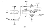
- FIG. 1 is a schematic diagram of a circuit structure of a shift register according to some embodiments of the present disclosure
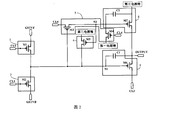
- FIG. 2 is a schematic diagram of a circuit structure of a shift register according to some embodiments of the present disclosure
- FIG. 3 is a timing chart showing the operation of the shift register shown in FIG. 2 when performing forward scanning
- FIG. 4 is a timing chart of operation when the shift register shown in FIG. 2 performs reverse scanning
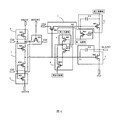
- FIG. 5 is a schematic diagram of a circuit structure of a shift register according to some embodiments of the present disclosure.
- FIG. 6 is a schematic structural diagram of a gate driving circuit according to some embodiments of the present disclosure.
- FIG. 7 is a timing chart when the gate driving circuit shown in FIG. 6 performs forward scanning
- FIG. 8 is a timing chart when the gate driving circuit shown in FIG. 6 performs reverse scanning
- FIG. 9 is a flowchart of a forward driving method of a shift register according to some embodiments of the present disclosure.
- FIG. 10 is a flowchart of a reverse driving method of a shift register according to some embodiments of the present disclosure.
- the GOA circuit is composed of a plurality of cascaded shift registers (Shift Register), and the output of each stage of the shift register is connected to the gate of the switching transistor in each row of pixel units to drive the pixel unit of the corresponding row.
- the shift register in the GOA circuit of the related art can only support one-way scanning (forward scanning or reverse scanning), and the bidirectional scanning function cannot be realized, which has certain limitations.
- FIG. 1 is a circuit diagram of a shift register provided in accordance with some embodiments of the present disclosure.
- the shift register includes a first input unit 1, a second input unit 2, a pull-up control unit 3, a pull-down control unit 4, an output control unit 5, an output reset unit 6, and a first control signal input end.
- the first input unit 1, the second input unit 2, the pull-up control unit 3, the pull-down control unit 4, and the output control unit 5 are connected to the first node N1, the pull-up control unit 3, the pull-down control unit 4, and the output reset unit. 6 is connected to the second node N2.
- the first input unit 1 is configured to input the positive sweep input signal provided by the positive sweep input signal terminal GSTVF to the first node N1 under the control of the control signal provided by the first control signal input terminal CL1.
- the second input unit 2 is configured to input the anti-sweep input signal provided by the anti-sweep input signal terminal GSTVB to the first node N1 under the control of the control signal provided by the third control signal input terminal CL3.
- the pull-up control unit 3 For controlling the potential of the first node N1, the pull-up control unit 3 inputs the control signal provided by the fourth control signal input terminal CL4 to the second node N2, or is provided at the fourth control signal input terminal CL4. Under the control of the control signal, the pull-up control unit 3 inputs the first voltage supplied from the first power supply terminal to the second node N2.
- the pull-down control unit 4 is for inputting the second voltage supplied from the second power terminal to the first node N1.
- the output control unit 5 is configured to input a control signal provided by the second control signal input terminal CL2 to the signal output terminal OUTPUT for the signal output terminal OUTPUT to output a scan signal.
- the output reset unit 6 is for inputting the third voltage supplied from the third power terminal to the signal output terminal OUTPUT to reset the signal output terminal OUTPUT.
- the operation process of the shift register includes three stages: an input stage and an output. Phase and reset phase.
- the first input unit 1 inputs the positive sweep input signal provided by the positive sweep input signal terminal GSTVF to the first node N1; Under the control of the potential of the node N1, the pull-up control unit 3 is for inputting the control signal supplied from the fourth control signal input terminal CL4 to the second node N2.
- the output control unit 5 sends a control signal in the second control signal input terminal CL2 to the signal output terminal OUTPUT for the signal output terminal OUTPUT to output the scan signal.
- the pull-up control unit 3 inputs the first voltage supplied from the first power supply terminal to the second node N2; the potential at the second node N2
- the output reset unit 6 inputs the third voltage supplied from the third power terminal to the signal output terminal OUTPUT to reset the signal output terminal OUTPUT.
- the shift register operation When the gate drive circuit is reverse-scanned (driving from the last gate line to the first gate line one by one), the shift register operation also includes three phases: an input phase, an output phase, and a reset phase.
- the second input unit 2 inputs the anti-sweep input signal provided by the anti-sweep input signal terminal GSTVB to the first node N1; Under the control of the potential of the node N1, the pull-up control unit 3 is for inputting the control signal supplied from the fourth control signal input terminal CL4 to the second node N2.
- the output control unit 5 In the output phase T2, under the control of the potential of the first node N1, the output control unit 5 sends a control signal in the second control signal input terminal CL2 to the signal output terminal OUTPUT for the signal output terminal OUTPUT to output the scan signal.
- the pull-up control unit 3 inputs the first voltage supplied from the first power supply terminal to the second node N2; at the second node N2 Under the control of the potential, the output reset unit 6 inputs the third voltage supplied from the third power terminal to the signal output terminal OUTPUT to reset the signal output terminal OUTPUT.
- the control signal provided by the first control signal input terminal CL1, the control signal provided by the second control signal input terminal CL2, the control signal provided by the third control signal input terminal CL3, and the fourth At least one of the control signals provided by the control signal input terminal CL4 is a clock signal, that is, a control signal corresponding to the input terminal is generated by the control of the phase relationship of the clock signal, so that no additional high voltage control signal is required, so that the circuit structure is simple.
- control signal provided by the first control signal input terminal CL1, the control signal provided by the second control signal input terminal CL2, the control signal provided by the third control signal input terminal CL3, and the The control signals provided by the four control signal input terminals CL4 are all clock signals. This eliminates the need for additional high voltage control signals and allows for a simple circuit structure.
- the technical solution of the present disclosure provides a positive scan input signal and a reverse scan input signal for the first node N1 by setting two input units, so that the shift register can realize bidirectional scanning, thereby enabling gate driving.
- the circuit implements forward and reverse scans.
- FIG. 2 is a schematic diagram of a circuit structure of a shift register according to some embodiments of the present disclosure.
- the shift register shown in FIG. 2 is an embodiment based on the shift register shown in FIG. 1.
- the first input unit 1 includes a first transistor M1.
- the control electrode of the first transistor M1 is connected to the first control signal input terminal CL1, the first electrode is connected to the positive scan input signal terminal GSTTV, and the second electrode is connected to the first node N1.
- the second input unit 2 includes a second transistor M2.
- the control electrode of the second transistor M2 is connected to the third control signal input terminal CL3, the first pole is connected to the reverse scan input signal terminal GSTVB, and the second pole is connected to the first node N1.
- the two input units are respectively two independent transistors for inputting the positive sweep input signal or the back sweep signal to the first node N1 under the control of the control signal provided by the corresponding control signal input end. .
- the pull up control unit 3 includes a third transistor M3 and a fourth transistor M4.
- the control electrode of the third transistor M3 is connected to the first node N1, the first pole is connected to the fourth control signal input terminal CL4, and the second pole is connected to the second node N2.
- the control electrode of the fourth transistor M4 is connected to the fourth control signal input terminal CL4, the first pole is connected to the first power terminal, and the second pole is connected to the second node N2.
- the pull-down control unit 4 includes a fifth transistor M5.
- the control electrode of the fifth transistor M5 is connected to the second node N2, the first pole is connected to the second power terminal, and the second pole is connected to the first node N1.
- the output control unit 5 includes a sixth transistor M6 and a first capacitor C1.
- the control electrode of the sixth transistor M6 is connected to the first node N1, the first electrode is connected to the second control signal input terminal CL2, and the second electrode is connected to the signal output terminal OUTPUT.
- the first end of the first capacitor C1 is connected to the first node N1, and the second end is connected to the signal output terminal OUTPUT.
- the output reset unit 6 includes a seventh transistor M7 and a second capacitor C2.
- the control electrode of the seventh transistor M7 is connected to the second node N2, the first pole is connected to the third power terminal, and the second pole is connected to the signal output terminal OUTPUT.
- the first end of the second capacitor C2 is connected to the second node N2, and the second end is connected to the first pole of the seventh transistor M7.
- the transistor in the present disclosure may be a thin film transistor or a field effect transistor or other switching devices having the same characteristics.
- a transistor typically includes three poles: a gate, a source, and a drain.
- the source and drain of the transistor are structurally symmetrical, and are interchangeable as desired.
- the control electrode refers to the gate of the transistor, one of the first and second poles being the source and the other being the drain.
- transistors can be classified into N-type transistors and P-type transistors.
- the transistor is an N-type transistor, its turn-on voltage is a high level voltage, and the turn-off voltage is a low level voltage.
- the transistor is a P-type transistor, its turn-on voltage is a low level voltage, and the turn-off voltage is a high level voltage.
- the first power terminal provides a low operating voltage
- the second power terminal and the third power terminal provide a high operating voltage.
- the high level voltage is recorded as VH
- the low level voltage is recorded as VL
- the threshold voltage of the P type transistor is recorded as Vth (which is a negative value and slightly smaller than 0V).
- FIG. 3 is a timing chart showing the operation of the shift register shown in FIG. 2 when performing forward scanning. As shown in FIG. 3, when the gate driving circuit performs forward scanning, the first control signal input terminal CL1, the second control signal input terminal CL2, the third control signal input terminal CL3, and the fourth control signal input terminal CL4 are provided.
- the duty ratio (the ratio of the duration of the effective potential to the period in one cycle, the transistor in the present embodiment is a P-type transistor, the effective potential is a low level) is 25% of the clock signal (ie, clock)
- the signal is used as a control signal, and the clock signal provided by the first control signal input terminal CL1 is referenced, and the clock signal provided by the second control signal input terminal CL2 is delayed compared with the clock signal provided by the first control signal input terminal CL1 ( The start time of the output effective potential is delayed) Cycle, the clock signal provided by the third control signal input terminal CL3 is delayed compared to the clock signal provided by the first control signal input terminal CL1 Cycle, the clock signal provided by the fourth control signal input terminal CL4 is delayed compared to the clock signal provided by the first control signal input terminal CL1 Cycles.
- the positive sweep input signal provided by the positive sweep input signal terminal GSTVF is at a low level
- the reverse sweep input signal provided by the reverse sweep input signal terminal GSTVB is at a high level
- the control provided by the first control signal input terminal CL1 The signal is at a low level
- the control signal provided by the second control signal input terminal CL2 is at a high level
- the control signal provided by the third control signal input terminal CL3 is at a high level
- the control signal provided by the fourth control signal input terminal CL4 is at a high level. High level.
- the first transistor M1 Since the control signal provided by the first control signal input terminal CL1 is at a low level, and the control signal supplied from the third control signal input terminal CL3 is at a high level, the first transistor M1 is turned on, and the second transistor M2 is turned off. At this time, the positive scan input signal supplied from the positive scan input signal terminal GSTVT is written to the first node N1 through the first transistor M1. Since the positive sweep input signal is at a low level, a threshold loss occurs when the positive sweep input signal at a low level passes through the P-type transistor. At this time, the voltage of the first node N1 is VL+
- both the third transistor M3 and the sixth transistor M6 are turned on. Since the third transistor M3 is turned on, the control signal at the high level supplied from the fourth control signal input terminal CL4 is written to the second node N2 through the third transistor M3. Accordingly, the fifth transistor M5 and the seventh transistor M7 are turned off. At the same time, since the sixth transistor M6 is turned on, the control signal at the high level provided by the second control signal input terminal CL2 is transmitted to the signal output terminal OUTPUT through the sixth transistor M6, and the signal output terminal OUTPUT outputs a high level voltage. .
- the voltage of the first end of the first capacitor C1 is VL+
- the voltage of the second end is VH
- the voltage difference between the two ends is VH-VL-
- the positive sweep input signal provided by the positive sweep input signal terminal GSTVF is at a high level
- the reverse sweep input signal provided by the reverse sweep input signal terminal GSTVB is at a high level
- the control provided by the first control signal input terminal CL1 The signal is at a high level
- the control signal provided by the second control signal input terminal CL2 is at a low level
- the control signal provided by the third control signal input terminal CL3 is at a high level
- the control signal provided by the fourth control signal input terminal CL4 is at a high level. High level.
- the first transistor M1 Since the control signal supplied from the first control signal input terminal CL1 is at a high level, the first transistor M1 is turned off. Since the control signal supplied from the third control signal input terminal CL3 is at a high level, the second transistor M2 is turned off. At this time, the first node N1 is in a floating state.
- the signal output terminal OUTPUT outputs a low level whose voltage is VL. That is, the voltage at the second end of the capacitor drops from VH to VL. Under the bootstrap action of the first capacitor C1 (maintaining the voltage difference across the two ends), the voltage at the first end of the capacitor drops to 2VL-VH+
- the third transistor M3 is maintained in conduction, and the fourth transistor M4, the fifth transistor M5, and the seventh transistor M7 continue to maintain an off state.
- the reset phase T3 it specifically includes a first reset sub-phase t1 and a second reset sub-phase t2.
- the positive-sweep input signal provided by the positive-sweep input signal terminal GSTVF is at a high level
- the anti-sweep input signal provided by the anti-sweep input signal terminal GSTVB is at a low level
- the first control signal input terminal CL1 The provided control signal is at a high level
- the control signal provided by the second control signal input terminal CL2 is at a high level
- the control signal provided by the third control signal input terminal CL3 is at a low level
- the fourth control signal input terminal CL4 provides The control signal is at a high level.
- the control signal provided by the first control signal input terminal CL1 is at a high level, and the control signal supplied from the third control signal input terminal CL3 is at a low level, the first transistor M1 is turned off, and the second transistor M2 is turned on.
- the anti-sweep input signal provided by the anti-sweep input signal terminal GSTVB is written to the first node N1 through the second transistor M2. Since the anti-sweep input signal is at a low level, a threshold loss occurs when the low-voltage anti-sweep input signal passes through the P-type transistor, and the voltage of the first node N1 is VL+
- is still a low level voltage, and the third transistor M3 and the sixth transistor M6 are both maintained on.
- the control signal at the high level supplied from the second control signal input terminal CL2 is transmitted to the signal output terminal OUTPUT through the sixth transistor M6.
- the signal output terminal OUTPUT outputs a high level voltage to reset the signal output terminal OUTPUT.
- the third transistor M3 maintains an on state, and the fourth transistor M4, the fifth transistor M5, and the seventh transistor M7 continue to maintain an off state.
- the positive-sweep input signal provided by the positive-sweep input signal terminal GSTVF is at a high level
- the anti-sweep input signal provided by the anti-sweep input signal terminal GSTVB is at a high level
- the first control signal input terminal CL1 The provided control signal is at a high level
- the control signal provided by the second control signal input terminal CL2 is at a high level
- the control signal provided by the third control signal input terminal CL3 is at a high level
- the fourth control signal input terminal CL4 provides The control signal is at a low level.
- the control signal supplied from the first control signal input terminal CL1 is at a high level
- the control signal supplied from the third control signal input terminal CL3 is at a high level, and thus the first transistor M1 and the second transistor M2 are both turned off.
- the fourth transistor M4 Since the control signal supplied from the fourth control signal input terminal CL4 is at a low level, the fourth transistor M4 is turned on.
- the low-level operating voltage supplied from the first power supply terminal is written to the second node N2 through the fourth transistor M4.
- the voltage of the second node N2 is VL, and at this time, the fifth transistor M5 and the seventh transistor M7 are both turned on.
- the fifth transistor M5 Since the fifth transistor M5 is turned on, the high-level operating voltage supplied from the second power supply terminal is written to the first node N1 through the fifth transistor M5. The voltage of the first node N1 becomes VH, at which time the sixth transistor M6 is turned off.
- the seventh transistor M7 Since the seventh transistor M7 is turned on, the high-level operating voltage supplied from the third power terminal is written to the signal output terminal OUTPUT through the seventh transistor M7 to achieve a true reset process on the signal output terminal OUTPUT. At this time, the voltages of the first end and the second end of the first capacitor C1 are both VH.
- the shift register provided by the present disclosure can perform the steps of input, output, and reset through the above process.
- the method further includes: maintaining the phase T4, and during the sustaining phase T4, the shift register continuously outputs a high level.
- the maintenance phase T4 specifically includes four different working states: (1) the control signal provided by the first control signal input terminal CL1 is at a low level, and the control signal provided by the other control signal input terminal is at a high level; (2) The control signal provided by the control signal input terminal CL2 is at a low level, and the control signal provided by the other control signal input terminal is at a high level; (3) the control signal provided by the third control signal input terminal CL3 is at a low level, and other control The control signal provided by the signal input terminal is at a high level; (4) the control signal provided by the fourth control signal input terminal CL4 is at a low level, and the control signal provided by the other control signal input terminal is at a high level.
- the positive sweep input signal provided by the positive sweep input signal terminal GSTVF is always at a high level
- the reverse sweep input signal provided by the reverse sweep input signal terminal GSTVB is always at a high level.
- the first transistor M1 is turned on.
- the positive sweep input signal GSTVF at a high level is written to the first node N1 through the first transistor M1 to maintain the voltage of the first node N1 at VH (the sixth transistor M6 remains off).
- the voltage of the signal output terminal OUTPUT can be maintained at VH.
- the second transistor M2 is turned on.
- the anti-sweep input signal GSTVB at a high level is written to the first node N1 through the second transistor M2 to maintain the voltage of the first node N1 at VH.
- the voltage of the signal output terminal OUTPUT can be maintained at VH.
- the fourth transistor M4 is turned on.
- the low-level operating voltage supplied from the first power supply terminal is written to the second node N2 through the fourth transistor M4.
- the fifth transistor M5 is turned on.
- the high-level operating voltage supplied from the second power supply terminal is written to the first node N1 through the fifth transistor M5 to maintain the voltage of the first node N1 at VH.
- the voltage of the signal output terminal OUTPUT can be maintained at VH.
- the voltage of the first node N1 is maintained at VH by the positive sweep input signal, the reverse sweep input signal, and the high-level operating voltage supplied from the second power supply terminal, respectively.
- the voltage of the signal output terminal OUTPUT can be maintained at VH.
- the signal output terminal OUTPUT can be stably outputted with the high-level voltage until the positive-sweeping input signal becomes the low-level state, and the above-described input phase T1 is performed again.
- FIG. 4 is a timing chart showing the operation of the shift register shown in FIG. 2 when performing reverse scanning.
- the first control signal input terminal CL1, the second control signal input terminal CL2, the third control signal input terminal CL3, and the fourth control signal input terminal CL4 provide a period.
- the same clock signal with a duty ratio of 25% that is, the clock signal is used as the control signal
- the clock signal provided by the third control signal input terminal CL3 is used as a reference
- the clock signal provided by the second control signal input terminal CL2 is compared.
- the clock signal provided by the first control signal input terminal CL1 is delayed compared to the clock signal provided by the third control signal input terminal CL3 Cycle
- the clock signal provided by the fourth control signal input terminal CL4 is delayed compared to the clock signal provided by the third control signal input terminal CL3 Cycles.
- the positive sweep input signal provided by the positive sweep input signal terminal GSTVF is at a high level
- the reverse sweep input signal provided by the reverse sweep input signal terminal GSTVB is at a low level
- the control provided by the first control signal input terminal CL1 is provided.
- the signal is at a high level
- the control signal provided by the second control signal input terminal CL2 is at a high level
- the control signal provided by the third control signal input terminal CL3 is at a low level
- the control signal provided by the fourth control signal input terminal CL4 is at a high level. High level.
- the first transistor M1 Since the control signal provided by the first control signal input terminal CL1 is at a high level, and the control signal supplied from the third control signal input terminal CL3 is at a low level, the first transistor M1 is turned off, and the second transistor M2 is turned on. At this time, the anti-sweep input signal provided by the anti-sweep input signal terminal GSTVB is written to the first node N1 through the second transistor M2. Since the anti-sweep input signal is at a low level, a threshold loss occurs when the low-voltage anti-sweep input signal passes through the P-type transistor. At this time, the voltage of the first node N1 is VL+
- both the third transistor M3 and the sixth transistor M6 are turned on. Since the third transistor M3 is turned on, the control signal at the high level supplied from the fourth control signal input terminal CL4 is written to the second node N2 through the third transistor M3. Accordingly, the fifth transistor M5 and the seventh transistor M7 are turned off. At the same time, since the sixth transistor M6 is turned on, the control signal at the high level provided by the second control signal input terminal CL2 is transmitted to the signal output terminal OUTPUT through the sixth transistor M6, and the signal output terminal OUTPUT outputs a high level voltage. .
- the voltage of the first end of the first capacitor C1 is VL+
- the voltage of the second end is VH
- the voltage difference between the two ends is VH-VL-
- the positive sweep input signal provided by the positive sweep input signal terminal GSTVF is at a high level
- the reverse sweep input signal provided by the reverse sweep input signal terminal GSTVB is at a high level
- the control provided by the first control signal input terminal CL1 The signal is at a high level
- the control signal provided by the second control signal input terminal CL2 is at a low level
- the control signal provided by the third control signal input terminal CL3 is at a high level
- the control signal provided by the fourth control signal input terminal CL4 is at a high level. High level.
- the first transistor M1 Since the control signal supplied from the first control signal input terminal CL1 is at a high level, the first transistor M1 is turned off. Since the control signal supplied from the third control signal input terminal CL3 is at a high level, the second transistor M2 is turned off. At this time, the first node N1 is in a floating state.
- the signal output terminal OUTPUT outputs a low level whose voltage is VL. That is, the voltage at the second end of the capacitor drops from VH to VL. Under the bootstrap action of the first capacitor C1 (maintaining the voltage difference across the two ends), the voltage at the first end of the capacitor drops to 2VL-VH+
- the third transistor M3 maintains an on state, and the fourth transistor M4, the fifth transistor M5, and the seventh transistor M7 continue to maintain an off state.
- the reset phase T3 it specifically includes a first reset sub-phase t1 and a second reset sub-phase t2.
- the positive-sweep input signal provided by the positive-sweep input signal terminal GSTVF is at a low level
- the anti-sweep input signal provided by the anti-sweep input signal terminal GSTVB is at a high level
- the first control signal input terminal CL1 The provided control signal is at a low level
- the control signal provided by the second control signal input terminal CL2 is at a high level
- the control signal provided by the third control signal input terminal CL3 is at a high level
- the fourth control signal input terminal CL4 provides The control signal is at a high level.
- the control signal provided by the first control signal input terminal CL1 is at a low level, and the control signal supplied from the third control signal input terminal CL3 is at a high level, the first transistor M1 is turned on, and the second transistor M2 is turned off.
- the positive scan input signal supplied from the input signal terminal GSTVF is written to the first node N1 through the first transistor M1.
- a threshold loss occurs when the positive sweep input signal at a low level passes through the P-type transistor.
- the voltage of the first node N1 is VL+
- is still a low level voltage, and the third transistor M3 and the sixth transistor M6 are both maintained on.
- the control signal at the high level provided by the second control signal input terminal CL2 is transmitted to the signal output terminal OUTPUT through the sixth transistor M6 to reset the signal output terminal OUTPUT.
- the third transistor M3 maintains an on state, and the fourth transistor M4, the fifth transistor M5, and the seventh transistor M7 continue to maintain an off state.
- the positive-sweep input signal provided by the positive-sweep input signal terminal GSTVF is at a high level
- the anti-sweep input signal provided by the anti-sweep input signal terminal GSTVB is at a high level
- the first control signal input terminal CL1 The provided control signal is at a high level
- the control signal provided by the second control signal input terminal CL2 is at a high level
- the control signal provided by the third control signal input terminal CL3 is at a high level
- the fourth control signal input terminal CL4 provides The control signal is at a low level.
- the control signal supplied from the first control signal input terminal CL1 is at a high level
- the control signal supplied from the third control signal input terminal CL3 is at a high level, and thus the first transistor M1 and the second transistor M2 are both turned off.
- the fourth transistor M4 Since the control signal supplied from the fourth control signal input terminal CL4 is at a low level, the fourth transistor M4 is turned on.
- the low-level operating voltage supplied from the first power supply terminal is written to the second node N2 through the fourth transistor M4.
- the voltage of the second node N2 is VL, and at this time, the fifth transistor M5 and the seventh transistor M7 are both turned on.
- the fifth transistor M5 Since the fifth transistor M5 is turned on, the high-level operating voltage supplied from the second power supply terminal is written to the first node N1 through the fifth transistor M5. The voltage of the first node N1 becomes VH, at which time the sixth transistor M6 is turned off.
- the seventh transistor M7 Since the seventh transistor M7 is turned on, the high-level operating voltage supplied from the third power terminal is written to the signal output terminal OUTPUT through the seventh transistor M7 to achieve a true reset process on the signal output terminal OUTPUT. At this time, the voltages of the first end and the second end of the first capacitor C1 are both VH.
- the shift register provided by the present disclosure can perform the steps of input, output, and reset through the above process.
- the sustain phase T4 may also be included after the reset phase T3.
- the shift register continues to output a high level during the sustain phase T4.
- the specific operation of the shift register in the sustain phase T4 during the reverse scan is the same as the specific operation of the shift register in the sustain phase T4 when performing the forward scan, and details are not described herein again.
- the signals provided in the input ends of the control signals are all clock signals, and no additional high voltage control signals are needed, thereby effectively reducing power consumption.
- the gate drive circuit can be forward-scanned or reverse-scanned for control. For details, refer to the subsequent description.
- FIG. 5 is a schematic diagram of a circuit structure of a shift register according to some embodiments of the present disclosure. As shown in FIG. 5, unlike the above embodiment, the shift register provided in this embodiment further includes a first current interrupting unit 7.
- the first current interrupting unit 7 is disposed between the output end of the first input unit 1 for outputting the positive scan input signal and the first node N1, and the output end of the second input unit 2 for outputting the anti-sweep input signal. Between a node N1.
- the first current interrupting unit 7 is configured to input a control signal of the effective potential provided by the second control signal input terminal CL2 to the signal output terminal OUTPUT (ie, Output phase T2), such that the first input unit 1 and the first node N1 and between the second input unit 2 and the first node N1 are disconnected to avoid leakage currents in the first input unit 1 and the second input unit 2 It affects the potential of the first node N1.
- the first current interrupting unit 7 includes an eighth transistor M8, a ninth transistor M9, and a tenth transistor M10.
- the control electrode of the eighth transistor M8 is connected to the signal output terminal OUTPUT, the first pole is connected to the second control signal input terminal CL2, and the second pole and the first input unit 1 are used for outputting the output end of the positive scan input signal and The output terminals of the two input units 2 for outputting the inverse scan input signals are all connected.
- the control electrode of the ninth transistor M9 is connected to the first control signal input terminal CL1, and the first electrode is connected to the output terminal of the first input unit 1 for outputting the positive scan input signal and the second electrode of the eighth transistor M8.
- the second pole is connected to the first node N1.
- the control electrode of the tenth transistor M10 is connected to the third control signal input terminal CL3, and the output terminals of the first and second input units 2 for outputting the inverse scan input signal are connected to the second electrode of the eighth transistor M8.
- the second pole is connected to the first node N1.
- the ninth transistor M9 and the first transistor M1 are symmetrically designed, and the second transistor M2 and the tenth transistor M10 are symmetrically designed, so that the circuit design can be simplified.
- the shift register provided in this embodiment further includes a second current intercepting unit 8.
- the second current interrupting unit 8 is disposed between the output end of the pull-down control unit 4 for outputting the second voltage and the first node N1.
- the second current interrupting unit 8 is configured to output the control signal of the effective potential provided by the second control signal input terminal CL2 to the signal output terminal OUTPUT when the output control unit 5 is under the control of the potential of the first node N1 (ie, output Stage T2) causes an open circuit between the output pull-down control unit 4 and the first node N1 to prevent the leakage current in the pull-down control unit 4 from affecting the potential of the first node N1.
- the second current interrupting unit 8 includes an eleventh transistor M11 and a twelfth transistor M12.
- the control electrode of the eleventh transistor M11 is connected to the second node N2, the first pole and the pull-down control unit 4 are connected to output the output end of the second voltage, and the second pole is connected to the first node N1.
- the control electrode of the twelfth transistor M12 is connected to the first node N1, the first pole is connected to the fourth power terminal, and the second pole and pull-down control unit 4 is configured to output the output terminal of the second voltage and the eleventh transistor M11.
- the first poles are connected.
- the fourth power supply terminal provides a low-level operating voltage VL.
- the eighth transistor M8 is turned off. Moreover, since the control signal provided by the first control signal input terminal CL1 is at a low level, and the control signal supplied from the third control signal input terminal CL3 is at a high level, the ninth transistor M9 is turned on, and the tenth transistor M10 is turned off.
- the positive sweep input signal GSTVF can be written to the first node N1 through the first transistor M1 and the ninth transistor M9 in sequence.
- the twelfth transistor M12 Since the first node N1 is at a low level, the twelfth transistor M12 is turned on. The low-level operating voltage supplied from the fourth power supply terminal is written to the first pole of the eleventh transistor M11 through the twelfth transistor M12. Also, since the second node N2 is at the high level at the input phase T1, the eleventh transistor M11 is turned off. The pull-down control unit 4 is disconnected from the first node N1, so that the leakage current in the pull-down control unit 4 can be prevented from affecting the potential of the first node N1. In addition, since the first pole and the second pole of the eleventh transistor M11 are both low-level voltages, the first node N1 does not discharge through the eleventh transistor M11.
- the eighth transistor M8 is turned on.
- the low level supplied from the second control line number input terminal CL2 is written to the first pole of the ninth transistor M9 and the first pole of the tenth transistor M10 through the eighth transistor M8.
- the control signal supplied from the third control signal input terminal CL3 is at the high level, so that the ninth transistor M9 and the tenth transistor M10 are both turned off.
- the first input unit 1 is disconnected from the first node N1 and the second input unit 2 is disconnected from the first node N1, so that the leakage current in the first input unit 1 and the second input unit 2 can be avoided to the first node.
- the potential of N1 is affected.
- the first pole and the second pole of the ninth transistor M9 are both low-level voltages
- the first pole and the second pole of the tenth transistor M10 are both low-level voltages, so the first node N1 does not
- the discharge is performed by the ninth transistor M9 or the tenth transistor M10.
- the twelfth transistor M12 is maintained on, the eleventh transistor M11 is maintained off, and the first and second poles of the eleventh transistor M11 are both low-level voltage, and the pull-down control unit 4 and the first node N1 When the circuit is disconnected, the first node N1 does not discharge through the eleventh transistor M11.
- each of the transistors connected to the first node N1 is in an off state, and discharge is not performed, so that the voltage of the first node N1 can be stabilized.
- the eighth transistor M8 is turned off. Further, since the control signal supplied from the first control signal input terminal CL1 is at a high level, and the control signal supplied from the third control signal input terminal CL3 is at a high level, the ninth transistor M9 and the tenth transistor M10 are both turned off.
- the twelfth transistor M12 is maintained in conduction. Since the second node N2 is at a high level, the eleventh transistor M11 is maintained off.
- the first current intercepting unit 7 and the second current interrupting unit 8 can also implement the first node N1 and the first input unit 1, the second input unit 2, and the pull-down in the output stage T2.
- the control unit 4 is disconnected to maintain the stability of the voltage of the first node N1, and the specific process will not be described herein.
- FIG. 6 is a schematic structural diagram of a gate driving circuit according to some embodiments of the present disclosure.
- the gate driving circuit includes a plurality of cascaded shift registers and a first clock signal line and a second clock signal line for respectively providing a clock signal connected to the plurality of cascaded shift registers. And a third clock signal line and a fourth clock signal line, wherein each shift register adopts the shift register provided in the above embodiment.
- the specific structure of the shift register will not be described here.
- the number of shift registers is 4N, and N is a preset positive integer.
- the signal output terminal OUTPUT of the shift register of the stage is opposite to the backsweep input signal terminal GSTVB of the previous stage shift register and the shift register of the subsequent stage.
- the sweep input signal terminal GSTVF is connected.
- the value of n is [1, N] and is a positive integer.
- the first control signal input terminal CL1 corresponding to the 4th-3th stage shift register SR_4n-3 is connected to the first clock signal line CK1, and the corresponding second control signal input terminal CL2 is connected to the second clock signal line CK2, corresponding to the
- the third control signal input terminal CL3 is connected to the third clock signal line CK3, and the corresponding fourth control signal input terminal CL4 is connected to the fourth clock signal line CK4.
- the first control signal input terminal CL1 corresponding to the 4th-2th stage shift register SR_4n-2 is connected to the second clock signal line CK2, and the corresponding second control signal input terminal CL2 is connected to the third clock signal line CK3, corresponding to the The three control signal input terminal CL3 is connected to the fourth clock signal line CK4, and the corresponding fourth control signal input terminal CL4 is connected to the first clock signal line CK1.
- the first control signal input terminal CL1 corresponding to the 4n-1th stage shift register SR_4n-1 is connected to the third clock signal line CK3, and the corresponding second control signal input terminal CL2 is connected to the fourth clock signal line CK4, corresponding to the
- the third control signal input terminal CL3 is connected to the first clock signal line CK1, and the corresponding fourth control signal input terminal CL4 is connected to the second clock signal line CK2.
- the first control signal input terminal CL1 corresponding to the 4th-stage shift register SR_4n is connected to the fourth clock signal line CK4, and the corresponding second control signal input terminal CL2 is connected to the first clock signal line CK1, and the corresponding third control signal input is input.
- the terminal CL3 is connected to the second clock signal line CK2, and the corresponding fourth control signal input terminal CL4 is connected to the third clock signal line CK3.
- FIG. 7 is a timing chart when the gate driving circuit shown in FIG. 6 performs forward scanning.
- the first clock signal line CK1, the second clock signal line CK2, the third clock signal line CK3, and the fourth clock signal line CK4 provide the same duty ratio.
- the transistor is a P-type transistor, the effective potential is a low-level voltage
- the clock signal provided by the first clock signal line CK1 is referenced, and the clock signal provided by the second clock signal line CK2 is delayed compared with the clock signal provided by the first clock signal line CK1.
- the clock signal provided by the third clock signal line CK3 is delayed compared to the clock signal provided by the first clock signal line CK1 Cycle
- the clock signal provided by the fourth clock signal line CK4 is delayed compared to the clock signal provided by the first clock signal line CK1 Cycles.
- the shift registers of the respective stages are input after the corresponding positive scanning input signal terminal GSTVF inputs the effective potential, and are provided at the corresponding second control signal input terminal CL2.
- the control signal is at the effective potential (taking the low level as the effective potential as an example)
- the shift register signal output terminal OUTPUT outputs the effective potential.
- the signal output terminal OUTPUT_1 of the first stage shift register SR_1 outputs a clock signal of an effective potential supplied from the second clock signal line CK2, and supplies a positive sweep input signal to the second stage shift register SR_2.
- the signal output terminal OUTPUT_2 of the second stage shift register SR_2 outputs a clock signal of an effective potential supplied from the third clock signal line CK3, and supplies a positive sweep input signal to the third stage shift register SR_3.
- the signal output terminal OUTPUT_3 of the third stage shift register SR_3 outputs a clock signal at the effective potential supplied from the fourth clock signal line CK4, and supplies a positive sweep input signal to the fourth stage shift register SR_4.
- the signal output terminal OUTPUT_4 of the fourth stage shift register SR_4 outputs a clock signal of an effective potential supplied from the first clock signal line CK1, and supplies a positive sweep input signal to the fifth stage shift register.
- the second control signal input terminal CL2 of the 4th-3th stage shift register SR_4n-3 is connected to the second clock signal line CK2, and provides a positive sweep input signal for the 4n-2th stage shift register SR_4n-2.
- the second control signal input terminal CL2 of the 4n-2th stage shift register SR_4n-2 is connected to the third clock signal line CK3, and supplies a positive sweep input signal to the 4n-1th stage shift register SR_4n-1.
- the second control signal input terminal CL2 of the 4n-1th stage shift register SR_4n-1 is connected to the fourth clock signal line CK4, and supplies a positive sweep input signal to the 4nth stage shift register SR_4n.
- the second control signal input terminal CL2 of the 4nth stage shift register SR_4n is connected to the first clock signal line CK1, and supplies a positive sweep input signal to the 4n+1th stage shift register SR_4n+1.
- the clock signals provided by the first clock signal line CK1, the second clock signal line CK2, the third clock signal line CK3, and the fourth clock signal line CK4 are sequentially delayed. Cycles, therefore, signal output of the 4n-3th shift register SR_4n-3, the 4n-2th shift register SR_4n-2, the 4n-1th shift register SR_4n-1, and the 4nth shift register SR_4n
- the terminal will sequentially output the effective potential, that is, perform a forward scan.
- FIG. 8 is a timing chart when the gate driving circuit shown in FIG. 6 performs reverse scanning.
- the first clock signal line CK1, the second clock signal line CK2, the third clock signal line CK3, and the fourth clock signal line CK4 provide the same duty ratio.
- the transistor is a P-type transistor, the effective potential is a low-level voltage
- the clock signal provided by the second clock signal line CK2 is delayed compared to the clock signal provided by the second clock signal line CK2.
- the clock signal provided by the fourth clock signal line CK4 is delayed compared to the clock signal provided by the second clock signal line CK2 Cycles
- the clock signal provided by the third clock signal line CK3 is delayed compared to the clock signal provided by the second clock signal line CK2 Cycles.
- the shift registers of each stage are input after the corresponding anti-sweep input signal terminal GSTVB inputs the effective potential, and are provided at the corresponding second control signal input terminal CL2.
- the control signal is at the effective potential (taking the low level as the effective potential as an example)
- the shift register signal output terminal OUTPUT outputs the effective potential.
- the signal output terminal OUTPUT_4N of the 4th-stage shift register outputs a clock signal of an effective potential supplied from the first clock signal line CK1, and supplies a back-sweep input signal to the 4N-1th stage shift register.
- the signal output terminal OUTPUT_4N-1 of the 4N-1th stage shift register outputs a clock signal at the effective potential supplied from the fourth clock signal line CK4, and supplies a backsweep input signal to the 4N-2th stage shift register.
- the signal output terminal OUTPUT_4N-2 of the 4N-2th stage shift register outputs a clock signal of an effective potential supplied from the third clock signal line CK3, and supplies a backsweep input signal to the 4N-3th stage shift register.
- the signal output terminal OUTPUT_4N-3 of the 4th N-3th shift register outputs a clock signal of an effective potential supplied from the second clock signal line CK2, and supplies a reverse sweep input signal to the 4th N-4th shift register.
- the 4nth stage shift register SR_4n outputs a clock signal at the effective potential supplied from the first clock signal line CK1, and supplies a backsweep input signal to the 4n-1th stage shift register SR_4n-1.
- the 4n-1th stage shift register SR_4n-1 outputs a clock signal at the effective potential supplied from the fourth clock signal line CK4, and supplies a backsweep input signal to the 4n-2th stage shift register SR_4n-2.
- the 4n-2th stage shift register SR_4n-2 outputs a clock signal of an effective potential supplied from the third clock signal line CK3, and supplies a backsweep input signal to the 4n-3th stage shift register SR_4n-3.
- the 4n-3th stage shift register SR_4n-3 outputs a clock signal of an effective potential supplied from the second clock signal line CK2, and supplies a backsweep input signal to the 4n-4th stage shift register SR_4n-4.
- the clock signals provided by the second clock signal line CK2, the first clock signal line CK1, the fourth clock signal line CK4, and the third clock signal line CK3 are sequentially delayed. Therefore, the 4th-stage shift register SR_4n, the 4n-1th shift register SR_4n-1, the 4n-2th shift register SR_4n-2, and the 4n-3 shift register SR_4n-3 are sequentially output.
- the effective potential is the reverse scan.
- the gate driving circuit provided by the present disclosure can realize forward scanning by sequentially controlling the first clock signal line CK1, the second clock signal line CK2, the third clock signal line CK3, and the fourth clock signal line CK4 to output an effective potential.
- the reverse scan can be realized by sequentially controlling the second clock signal line CK2, the first clock signal line CK1, the fourth clock signal line CK4, and the third clock signal line CK3 to output an effective potential. It can be seen that the gate driving circuit provided by the present disclosure can support the bidirectional scanning function.
- a display device employing the gate drive circuit as shown in FIG. 6 above.
- FIG. 9 is a flowchart of a forward driving method of a shift register according to some embodiments of the present disclosure. As shown in FIG. 9, wherein the shift register employs the shift register in the above embodiment, the forward driving method includes.
- Step S101 in the input stage, under the control of the control signal provided by the input of the first control signal, the first input unit inputs the positive scan input signal provided by the positive scan input signal terminal to the first node;
- the pull-up control unit is configured to input a control signal provided by the fourth control signal input terminal to the second node under the control of the potential.
- Step S102 In the output stage, under the control of the potential of the first node, the output control unit sends a control signal in the input end of the second control signal to the signal output end, so that the signal output end outputs the scan signal.
- Step S103 in the reset phase, under the control of the control signal provided by the fourth control signal input end, the pull-up control unit inputs the first voltage provided by the first power supply terminal to the second node; the potential of the second node Under control, the output reset unit inputs a third voltage provided by the third power terminal to the signal output terminal to reset the signal output terminal.
- FIG. 10 is a flowchart of a reverse driving method of a shift register according to some embodiments of the present disclosure. As shown in Fig. 10, wherein the shift register employs the shift register in the above embodiment, the reverse driving method includes.
- Step S201 in the input stage, under the control of the control signal provided by the input end of the third control signal, the second input unit inputs the anti-sweep input signal provided by the anti-sweep input signal terminal to the first node;
- the pull-up control unit is configured to input a control signal provided by the fourth control signal input terminal to the second node under the control of the potential.
- Step S202 In the output stage, under the control of the potential of the first node, the output control unit sends a control signal in the input end of the second control signal to the signal output end, so that the signal output end outputs the scan signal.
- Step S203 in the reset phase, under the control of the control signal provided by the fourth control signal input terminal, the pull-up control unit inputs the first voltage provided by the first power supply terminal to the second node; the potential of the second node Under control, the output reset unit inputs a third voltage provided by the third power terminal to the signal output terminal to reset the signal output terminal.
Landscapes
- Engineering & Computer Science (AREA)
- Physics & Mathematics (AREA)
- Computer Hardware Design (AREA)
- General Physics & Mathematics (AREA)
- Theoretical Computer Science (AREA)
- Microelectronics & Electronic Packaging (AREA)
- Power Engineering (AREA)
- Shift Register Type Memory (AREA)
- Control Of Indicators Other Than Cathode Ray Tubes (AREA)
- Liquid Crystal Display Device Control (AREA)
Abstract
L'invention concerne un registre à décalage, son procédé d'attaque, un circuit d'attaque de grille et un appareil d'affichage. Le registre à décalage comprend une première unité d'entrée, une seconde unité d'entrée, une unité de commande de rappel vers le niveau haut, une unité de commande de rappel vers le niveau bas, une unité de commande de sortie et une unité de réinitialisation de sortie. La première unité d'entrée, la seconde unité d'entrée, l'unité de commande de rappel vers le niveau haut, l'unité de commande de rappel vers le niveau bas et l'unité de commande de sortie sont connectées à un premier nœud, et l'unité de commande de rappel vers le niveau haut, l'unité de commande de rappel vers le niveau bas et l'unité de réinitialisation de sortie sont connectées à un second nœud.
Priority Applications (2)
| Application Number | Priority Date | Filing Date | Title |
|---|---|---|---|
| US16/622,099 US11094239B2 (en) | 2018-02-09 | 2019-01-25 | Shift register and driving method thereof, gate driving circuit and display device |
| US17/373,143 US11749156B2 (en) | 2018-02-09 | 2021-07-12 | Shift register and driving method thereof, gate driving circuit and display device |
Applications Claiming Priority (2)
| Application Number | Priority Date | Filing Date | Title |
|---|---|---|---|
| CN201810136139.7A CN109389927B (zh) | 2018-02-09 | 2018-02-09 | 移位寄存器及其驱动方法、栅极驱动电路 |
| CN201810136139.7 | 2018-02-09 |
Related Child Applications (2)
| Application Number | Title | Priority Date | Filing Date |
|---|---|---|---|
| US16/622,099 A-371-Of-International US11094239B2 (en) | 2018-02-09 | 2019-01-25 | Shift register and driving method thereof, gate driving circuit and display device |
| US17/373,143 Continuation US11749156B2 (en) | 2018-02-09 | 2021-07-12 | Shift register and driving method thereof, gate driving circuit and display device |
Publications (1)
| Publication Number | Publication Date |
|---|---|
| WO2019154122A1 true WO2019154122A1 (fr) | 2019-08-15 |
Family
ID=65416507
Family Applications (1)
| Application Number | Title | Priority Date | Filing Date |
|---|---|---|---|
| PCT/CN2019/073151 Ceased WO2019154122A1 (fr) | 2018-02-09 | 2019-01-25 | Registre à décalage, son procédé d'attaque, circuit d'attaque de grille et appareil d'affichage |
Country Status (3)
| Country | Link |
|---|---|
| US (2) | US11094239B2 (fr) |
| CN (1) | CN109389927B (fr) |
| WO (1) | WO2019154122A1 (fr) |
Families Citing this family (10)
| Publication number | Priority date | Publication date | Assignee | Title |
|---|---|---|---|---|
| CN109389927B (zh) * | 2018-02-09 | 2020-04-24 | 京东方科技集团股份有限公司 | 移位寄存器及其驱动方法、栅极驱动电路 |
| CN109192171A (zh) * | 2018-10-24 | 2019-01-11 | 京东方科技集团股份有限公司 | 移位寄存器单元及驱动方法、栅极驱动电路、显示装置 |
| US11308854B2 (en) | 2019-03-22 | 2022-04-19 | Boe Technology Group Co., Ltd. | Shift register unit, driving circuit, display device and driving method |
| CN110189676B (zh) * | 2019-05-31 | 2021-04-02 | 京东方科技集团股份有限公司 | 移位寄存器单元及驱动方法、栅极驱动电路、显示面板 |
| CN113838398B (zh) | 2020-06-24 | 2023-07-18 | 京东方科技集团股份有限公司 | 显示面板、显示装置 |
| CN111768741A (zh) * | 2020-06-24 | 2020-10-13 | 京东方科技集团股份有限公司 | 一种移位寄存器、栅极驱动电路及显示面板 |
| CN111627372B (zh) * | 2020-06-30 | 2022-07-26 | 武汉天马微电子有限公司 | 一种移位寄存器及其电路、显示面板和电子设备 |
| KR20220081141A (ko) * | 2020-12-08 | 2022-06-15 | 주식회사 엘엑스세미콘 | 무라를 보상하기 위한 보상 데이터 생성 장치 및 보상 데이터를 이용하는 디스플레이의 무라 보상 장치 |
| CN113192454B (zh) * | 2021-05-14 | 2023-08-01 | 武汉天马微电子有限公司 | 扫描驱动电路、方法、显示面板和显示装置 |
| CN117063237A (zh) * | 2022-03-14 | 2023-11-14 | 京东方科技集团股份有限公司 | 移位寄存器单元及其驱动方法、栅极驱动电路及显示装置 |
Citations (4)
| Publication number | Priority date | Publication date | Assignee | Title |
|---|---|---|---|---|
| US20100328281A1 (en) * | 2009-06-26 | 2010-12-30 | Hitachi Displays, Ltd. | Driver circuit controlling threshold voltage shift of transistor |
| CN102855858A (zh) * | 2012-09-03 | 2013-01-02 | 京东方科技集团股份有限公司 | 一种双向扫描控制开关、栅极驱动电路及工作方法 |
| CN103035296A (zh) * | 2011-10-04 | 2013-04-10 | 乐金显示有限公司 | 双向移位寄存器 |
| CN104834427A (zh) * | 2015-05-27 | 2015-08-12 | 京东方科技集团股份有限公司 | 触控驱动电路及其驱动方法、阵列基板及触控显示装置 |
Family Cites Families (5)
| Publication number | Priority date | Publication date | Assignee | Title |
|---|---|---|---|---|
| KR101155899B1 (ko) * | 2010-05-07 | 2012-06-20 | 삼성모바일디스플레이주식회사 | 주사 구동 장치 및 그 구동 방법 |
| CN102629444B (zh) * | 2011-08-22 | 2014-06-25 | 北京京东方光电科技有限公司 | 栅极集成驱动电路、移位寄存器及显示屏 |
| CN106023919B (zh) * | 2016-06-30 | 2019-01-18 | 京东方科技集团股份有限公司 | 移位寄存器及其驱动方法、驱动电路和显示装置 |
| CN106297697B (zh) * | 2016-08-29 | 2017-09-15 | 京东方科技集团股份有限公司 | 移位寄存器及其操作方法 |
| CN109389927B (zh) * | 2018-02-09 | 2020-04-24 | 京东方科技集团股份有限公司 | 移位寄存器及其驱动方法、栅极驱动电路 |
-
2018
- 2018-02-09 CN CN201810136139.7A patent/CN109389927B/zh active Active
-
2019
- 2019-01-25 US US16/622,099 patent/US11094239B2/en active Active
- 2019-01-25 WO PCT/CN2019/073151 patent/WO2019154122A1/fr not_active Ceased
-
2021
- 2021-07-12 US US17/373,143 patent/US11749156B2/en active Active
Patent Citations (4)
| Publication number | Priority date | Publication date | Assignee | Title |
|---|---|---|---|---|
| US20100328281A1 (en) * | 2009-06-26 | 2010-12-30 | Hitachi Displays, Ltd. | Driver circuit controlling threshold voltage shift of transistor |
| CN103035296A (zh) * | 2011-10-04 | 2013-04-10 | 乐金显示有限公司 | 双向移位寄存器 |
| CN102855858A (zh) * | 2012-09-03 | 2013-01-02 | 京东方科技集团股份有限公司 | 一种双向扫描控制开关、栅极驱动电路及工作方法 |
| CN104834427A (zh) * | 2015-05-27 | 2015-08-12 | 京东方科技集团股份有限公司 | 触控驱动电路及其驱动方法、阵列基板及触控显示装置 |
Also Published As
| Publication number | Publication date |
|---|---|
| CN109389927B (zh) | 2020-04-24 |
| US20210343216A1 (en) | 2021-11-04 |
| US11094239B2 (en) | 2021-08-17 |
| US20200184873A1 (en) | 2020-06-11 |
| US11749156B2 (en) | 2023-09-05 |
| CN109389927A (zh) | 2019-02-26 |
Similar Documents
| Publication | Publication Date | Title |
|---|---|---|
| WO2019154122A1 (fr) | Registre à décalage, son procédé d'attaque, circuit d'attaque de grille et appareil d'affichage | |
| CN112687230B (zh) | 移位寄存器、栅极驱动电路和显示面板 | |
| CN110164352B (zh) | 移位寄存器电路及其驱动方法、栅极驱动电路和显示面板 | |
| CN110264948B (zh) | 移位寄存器单元、驱动方法、栅极驱动电路及显示装置 | |
| CN108573668B (zh) | 移位寄存器单元及其驱动方法、栅极驱动电路及显示装置 | |
| CN109285504B (zh) | 移位寄存器单元及其驱动方法、栅极驱动电路 | |
| CN106782285B (zh) | 移位寄存器单元及其驱动方法、栅极驱动电路及显示装置 | |
| WO2018040711A1 (fr) | Registre à décalage et son procédé d'attaque, circuit d'attaque de grille et dispositif d'affichage | |
| WO2018205543A1 (fr) | Registre à décalage, son procédé d'attaque, circuit d'attaque intégré à une grille et dispositif d'affichage | |
| WO2019007043A1 (fr) | Circuit d'unité d'attaque de grille et procédé d'attaque associé, circuit d'attaque de grille et appareil d'affichage | |
| WO2010050262A1 (fr) | Circuit de registre à décalage, dispositif d’affichage et procédé de commande de circuit de registre à décalage | |
| CN102479477A (zh) | 移位寄存器单元、栅极驱动电路和显示装置 | |
| CN107516505B (zh) | 移位寄存器单元及其驱动方法、栅极驱动电路和显示面板 | |
| WO2017016190A1 (fr) | Registre à décalage, dispositif d'affichage et procédé de commande de registre à décalage | |
| CN113053447A (zh) | 移位寄存器单元、驱动方法、栅极驱动电路及显示装置 | |
| CN110197697B (zh) | 移位寄存器、栅极驱动电路以及显示设备 | |
| CN120356442B (zh) | 降噪电路和栅极驱动电路 | |
| WO2017067376A1 (fr) | Unité de registre à décalage, dispositif de pilotage de grille, dispositif d'affichage et procédé de commande | |
| WO2018196291A1 (fr) | Unité de registre à décalage et procédé d'attaque associé, registre à décalage, et dispositif d'affichage | |
| CN106683617A (zh) | 移位寄存器单元、阵列基板和显示装置 | |
| CN113744693B (zh) | 移位寄存器、栅极驱动器、显示面板和显示装置 | |
| US11328785B2 (en) | Shift register, gate driving circuit and gate driving method | |
| TWI701657B (zh) | 移位暫存器與相關的顯示裝置 | |
| CN117642798B (zh) | 移位寄存器、栅极驱动电路和显示装置 | |
| CN119993067B (zh) | 栅极驱动电路及显示面板 |
Legal Events
| Date | Code | Title | Description |
|---|---|---|---|
| 121 | Ep: the epo has been informed by wipo that ep was designated in this application |
Ref document number: 19751238 Country of ref document: EP Kind code of ref document: A1 |
|
| NENP | Non-entry into the national phase |
Ref country code: DE |
|
| 32PN | Ep: public notification in the ep bulletin as address of the adressee cannot be established |
Free format text: NOTING OF LOSS OF RIGHTS PURSUANT TO RULE 112(1) EPC (EPO FORM 1205A DATED 01.12.2020) |
|
| 122 | Ep: pct application non-entry in european phase |
Ref document number: 19751238 Country of ref document: EP Kind code of ref document: A1 |