WO2019159727A1 - Dispositif à semi-conducteur et son procédé de fabrication - Google Patents
Dispositif à semi-conducteur et son procédé de fabrication Download PDFInfo
- Publication number
- WO2019159727A1 WO2019159727A1 PCT/JP2019/003774 JP2019003774W WO2019159727A1 WO 2019159727 A1 WO2019159727 A1 WO 2019159727A1 JP 2019003774 W JP2019003774 W JP 2019003774W WO 2019159727 A1 WO2019159727 A1 WO 2019159727A1
- Authority
- WO
- WIPO (PCT)
- Prior art keywords
- semiconductor device
- antenna
- article
- semiconductor
- semiconductor chip
- Prior art date
- Legal status (The legal status is an assumption and is not a legal conclusion. Google has not performed a legal analysis and makes no representation as to the accuracy of the status listed.)
- Ceased
Links
Images






Classifications
-
- G—PHYSICS
- G06—COMPUTING OR CALCULATING; COUNTING
- G06K—GRAPHICAL DATA READING; PRESENTATION OF DATA; RECORD CARRIERS; HANDLING RECORD CARRIERS
- G06K19/00—Record carriers for use with machines and with at least a part designed to carry digital markings
- G06K19/06—Record carriers for use with machines and with at least a part designed to carry digital markings characterised by the kind of the digital marking, e.g. shape, nature, code
- G06K19/067—Record carriers with conductive marks, printed circuits or semiconductor circuit elements, e.g. credit or identity cards also with resonating or responding marks without active components
- G06K19/07—Record carriers with conductive marks, printed circuits or semiconductor circuit elements, e.g. credit or identity cards also with resonating or responding marks without active components with integrated circuit chips
- G06K19/077—Constructional details, e.g. mounting of circuits in the carrier
- G06K19/07749—Constructional details, e.g. mounting of circuits in the carrier the record carrier being capable of non-contact communication, e.g. constructional details of the antenna of a non-contact smart card
- G06K19/07758—Constructional details, e.g. mounting of circuits in the carrier the record carrier being capable of non-contact communication, e.g. constructional details of the antenna of a non-contact smart card arrangements for adhering the record carrier to further objects or living beings, functioning as an identification tag
-
- G—PHYSICS
- G06—COMPUTING OR CALCULATING; COUNTING
- G06K—GRAPHICAL DATA READING; PRESENTATION OF DATA; RECORD CARRIERS; HANDLING RECORD CARRIERS
- G06K19/00—Record carriers for use with machines and with at least a part designed to carry digital markings
- G06K19/06—Record carriers for use with machines and with at least a part designed to carry digital markings characterised by the kind of the digital marking, e.g. shape, nature, code
- G06K19/067—Record carriers with conductive marks, printed circuits or semiconductor circuit elements, e.g. credit or identity cards also with resonating or responding marks without active components
- G06K19/07—Record carriers with conductive marks, printed circuits or semiconductor circuit elements, e.g. credit or identity cards also with resonating or responding marks without active components with integrated circuit chips
- G06K19/077—Constructional details, e.g. mounting of circuits in the carrier
- G06K19/0772—Physical layout of the record carrier
- G06K19/07722—Physical layout of the record carrier the record carrier being multilayered, e.g. laminated sheets
-
- H—ELECTRICITY
- H01—ELECTRIC ELEMENTS
- H01Q—ANTENNAS, i.e. RADIO AERIALS
- H01Q1/00—Details of, or arrangements associated with, antennas
- H01Q1/12—Supports; Mounting means
- H01Q1/22—Supports; Mounting means by structural association with other equipment or articles
-
- H—ELECTRICITY
- H01—ELECTRIC ELEMENTS
- H01Q—ANTENNAS, i.e. RADIO AERIALS
- H01Q1/00—Details of, or arrangements associated with, antennas
- H01Q1/12—Supports; Mounting means
- H01Q1/22—Supports; Mounting means by structural association with other equipment or articles
- H01Q1/2208—Supports; Mounting means by structural association with other equipment or articles associated with components used in interrogation type services, i.e. in systems for information exchange between an interrogator/reader and a tag/transponder, e.g. in Radio Frequency Identification [RFID] systems
-
- H—ELECTRICITY
- H01—ELECTRIC ELEMENTS
- H01Q—ANTENNAS, i.e. RADIO AERIALS
- H01Q1/00—Details of, or arrangements associated with, antennas
- H01Q1/12—Supports; Mounting means
- H01Q1/22—Supports; Mounting means by structural association with other equipment or articles
- H01Q1/2283—Supports; Mounting means by structural association with other equipment or articles mounted in or on the surface of a semiconductor substrate as a chip-type antenna or integrated with other components into an IC package
-
- H—ELECTRICITY
- H10—SEMICONDUCTOR DEVICES; ELECTRIC SOLID-STATE DEVICES NOT OTHERWISE PROVIDED FOR
- H10D—INORGANIC ELECTRIC SEMICONDUCTOR DEVICES
- H10D30/00—Field-effect transistors [FET]
- H10D30/60—Insulated-gate field-effect transistors [IGFET]
- H10D30/67—Thin-film transistors [TFT]
-
- H—ELECTRICITY
- H10—SEMICONDUCTOR DEVICES; ELECTRIC SOLID-STATE DEVICES NOT OTHERWISE PROVIDED FOR
- H10D—INORGANIC ELECTRIC SEMICONDUCTOR DEVICES
- H10D86/00—Integrated devices formed in or on insulating or conducting substrates, e.g. formed in silicon-on-insulator [SOI] substrates or on stainless steel or glass substrates
- H10D86/80—Integrated devices formed in or on insulating or conducting substrates, e.g. formed in silicon-on-insulator [SOI] substrates or on stainless steel or glass substrates characterised by multiple passive components, e.g. resistors, capacitors or inductors
Definitions
- the present disclosure relates to a semiconductor device (particularly, a wireless communication semiconductor device) such as an RFID (radio frequency identification) tag and an IC (integrated circuit) tag, and a manufacturing method thereof.
- a semiconductor device particularly, a wireless communication semiconductor device
- RFID radio frequency identification
- IC integrated circuit
- wireless communication semiconductor devices are distributed (distribution management), production management, inventory management, location management, history in retail, apparel, transportation, and publishing (libraries), such as convenience stores and supermarkets. Very useful for management.
- the wireless communication semiconductor device typically includes an IC chip including a silicon chip mounted on a circuit board and an antenna.
- An IC chip typically includes a radio circuit unit that processes a received wave received by an antenna; a memory unit that stores a received signal in the radio circuit unit; a power supply circuit unit that generates drive power; and a received signal in the memory unit.
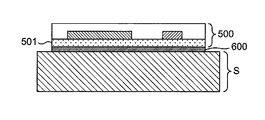
- the inventors of the present disclosure naturally use a conventional semiconductor device (particularly a wireless communication semiconductor device) 500 that is attached to an article S with an adhesive layer 600. I found a new problem that there is a risk of peeling or artificial peeling. In addition, since a semiconductor device (particularly a wireless communication semiconductor device) is attached by a person or a robot, it is a very complicated operation.
- Patent Document 3 discloses a technique in which an antenna is formed on a prescription and the tag body is bonded to the antenna surface with an adhesive layer. However, even in such a technique, the adhesive layer is used. Bonding (sticking) was still a complicated task.
- the present disclosure relates to a semiconductor device and a manufacturing method thereof that can improve the safety against peeling of a semiconductor device (for example, a wireless communication semiconductor device) from an article and can eliminate (omit) the operation of attaching the semiconductor device to the article.
- a semiconductor device for example, a wireless communication semiconductor device
- the purpose is to provide.
- One embodiment of the present disclosure is a semiconductor device including a semiconductor chip and an antenna, and the semiconductor chip and the antenna are directly fixed to a surface of an article, and the thickness direction of each is related to More than 1/2 of each height dimension is exposed from the surface of the article.
- Another embodiment of the present disclosure is a semiconductor device including a thin film transistor and an antenna, and the thin film transistor and the antenna are directly fixed to a surface of an article.
- Another aspect of the present disclosure is a semiconductor device including, on a base layer, at least one of a semiconductor chip and a thin film transistor and an antenna, wherein the at least one of the semiconductor chip and the thin film transistor and the antenna are It is directly fixed to the surface of the underlayer, and the underlayer is directly fixed to the surface of the article.
- Yet another aspect of the present disclosure is a method for manufacturing a semiconductor device including one or more components selected from the group consisting of a semiconductor chip, a thin film transistor, an antenna, and a wiring, and includes the following steps P1 and Q1 Including at least one of the steps: Mounting the semiconductor chip directly on the surface of the article P1; Step Q1 in which the one or more components selected from the group consisting of the thin film transistor, the antenna, and the wiring are directly formed on the surface of the article by a printing method.
- Yet another embodiment of the present disclosure is a method for manufacturing a semiconductor device including one or more components selected from the group consisting of a semiconductor chip, a thin film transistor, an antenna, and a wiring on a base layer, Step O, and at least one of steps P2 and Q2: Forming the underlayer directly on the surface of the article O; Mounting the semiconductor chip directly on the surface of the foundation layer P2; Step Q2 in which the one or more components selected from the group consisting of the thin film transistor, the antenna, and the wiring are directly formed on the surface of the underlayer by a printing method.
- the semiconductor device for example, a wireless communication semiconductor device
- the semiconductor device has improved safety against peeling of the semiconductor device from the article, and can eliminate (omit) the operation of attaching the semiconductor device to the article.
- the semiconductor device of the present disclosure may be any device including a semiconductor, for example, a wireless communication semiconductor device such as an RFID tag and an IC tag.
- a wireless communication semiconductor device such as an RFID tag and an IC tag.
- a wireless communication semiconductor device in particular is sometimes referred to as a “wireless communication device”.
- the semiconductor device 10 (for example, a wireless communication device) of the present disclosure is directly fixed to the surface of the article S as illustrated in FIG.
- the semiconductor device 10 is “directly fixed to the surface of the article S”.
- the semiconductor device 10 is a circuit board (501 in FIG. 5) used between conventional semiconductor devices. )
- an adhesive layer (indicated by 600 in FIG. 5) means that they are fixed without interposition. That is, the semiconductor device 10 of the present disclosure is a semiconductor device that is directly fixed to the surface of the article S, and a circuit board (a circuit board included in a conventional semiconductor device) is also attached to the article S. It is a semiconductor device that does not intervene (adhesive layer for attaching a conventional semiconductor device to an article).
- the semiconductor device of the present disclosure is formed or manufactured directly on the surface of an article without including a circuit board and without using an adhesive layer. For this reason, the semiconductor device of the present disclosure achieves space saving (or downsizing), and the manufacturing cost is further reduced. In addition, the degree of freedom in forming the antenna is increased.
- the semiconductor device of the present disclosure has a structure inseparable from an article. “Fixed” means that they are bonded or joined.
- a circuit board (indicated by reference numeral 501 in FIG. 5) that is not included in the semiconductor device of the present disclosure is attached with components such as a semiconductor chip, a thin film transistor (TFT), an antenna, or a wiring constituting the semiconductor device in the conventional semiconductor device. It is a sheet-like or plate-like component that is arranged, positioned, or held so that a semiconductor device can be distributed and traded as one product or commodity. Therefore, a circuit board in one semiconductor device is usually one continuous circuit board on which all components such as a semiconductor chip, a TFT, an antenna, and a wiring constituting the one semiconductor device are arranged. It has dimensions that can be held above.
- a polyester resin for example, polyethylene terephthalate resin
- polyimide resin for example, polyethylene resin, polypropylene resin
- polyphenylene sulfide resin polyvinyl formal resin, polyurethane resin
- polyamideimide resin A polymer substrate such as a polyamide resin; a glass substrate; a paper substrate; or a ceramic substrate is used.
- the thickness of the circuit board of the conventional semiconductor device is usually 0.1 ⁇ m or more and 2 mm or less, preferably 0.1 mm or more and 2 mm or less.
- An adhesive layer (indicated by 600 in FIG. 5) that is not used in the semiconductor device 10 of the present disclosure is a layer made of an adhesive used for attaching a conventional semiconductor device to an article.
- the article to which the semiconductor device of the present disclosure is fixed may be any product, or may be an intermediate obtained in the manufacturing process of such a product.
- the fixing can be performed in a series of manufacturing processes of the product, and the semiconductor device of the present disclosure is integrated with an article. It has an inseparable structure. For this reason, the safety
- Examples of the article include all products to which semiconductor devices (for example, wireless communication devices) are conventionally attached or intermediates thereof.
- a finished product that can be distributed on the market such as a tool, a medical instrument, a high-end brand product, and a container can be given.
- the semiconductor device of the present disclosure By fixing the semiconductor device of the present disclosure directly to the surface of a finished product that can be distributed on the market, the function of the semiconductor device can be imparted after the product is completed.
- the semiconductor device (for example, a wireless communication device) of the present disclosure can also be applied to rental articles such as bicycles, retail product packages, and apparel product tags.
- the article to which the semiconductor device of the present disclosure is fixed may have any shape.
- the surface of the article S to which the semiconductor device of the present disclosure is fixed has a planar shape in FIG. 1 and the like, but may have a three-dimensional shape.
- the antenna can be three-dimensional, and the influence of antenna directivity is reduced. And the receiving sensitivity of the antenna can be improved as a whole in all directions. It is generally difficult to read (receive) radio waves from the horizontal direction (in-plane direction of the plane) with planar antennas, but it is relatively easy to read (receive) radio waves from all directions with three-dimensional antennas. Can be achieved.
- the three-dimensional shape is a surface shape of the three-dimensional structure, and may be a non-planar shape such as a curved surface shape.
- the semiconductor device 10 includes one or more components selected from the group consisting of a semiconductor chip 2, a thin film transistor (TFT) 3, an antenna 4, a wiring 5, etc. It is said that).
- TFT thin film transistor
- antenna 4 a wiring 5, etc. It is said that).
- 3, 4, 5 means that the TFT 3, the antenna 4 or the wiring 5 may be used.
- the semiconductor device 10 of the present disclosure generally further includes a protective film 6 as shown in FIG.
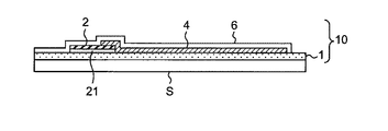
- FIG. 1 is a schematic cross-sectional view illustrating an example of the structure of the semiconductor device of the present disclosure.
- all components included in the semiconductor device 10 are directly fixed to the surface of the article S. As described in detail above, all the components are fixed to the article S without any circuit board or adhesive layer. Bonding is performed by directly forming a component on the surface of the article S by a printing method, a coating method, a vacuum film-forming method, or the like, thereby binding the printed material, the coating material, or the film-formed material to the surface by an intermolecular force or the like. May be achieved. Alternatively, the fixing may also be achieved by bonding the component to the surface of the article S by adhesive or the like, by bonding the component to the surface of the article S with an adhesive or the like.
- the components other than the semiconductor chip 2 are fixed by bonding by intermolecular force and the like.
- the fixing of the chip 2 is preferably achieved by bonding by adhesive force or the like.
- the semiconductor device 10 includes the semiconductor chip 2
- the semiconductor chip 2 is directly mounted on the surface of the article S, and as a result, the adhesive layer 21 for mounting between the article S (see FIG. 3C).
- the adhesive layer 21 for mounting between the article S is bonded or bonded to the surface of the article S without any circuit board or adhesive layer.
- “Mounting” refers to bonding semiconductor chips manufactured or obtained in advance with an adhesive.
- the “adhesive layer” is a layer made of an adhesive conventionally used for mounting a semiconductor chip.
- the adhesive rubber adhesives, epoxy resins, hot melt adhesives and the like are usually used.
- the semiconductor chip is directly mounted on the surface of the article. “Mounting” means, in addition, that the semiconductor chip is bonded to the surface of the article in such a manner that the semiconductor chip is exposed from the surface of the article by 1/2 or more of the height dimension of the semiconductor chip. For example, an embodiment (embedding) in which a semiconductor chip is embedded in an article is not included.
- the TFT 3 is directly formed on the surface of the article S.
- the circuit board and the adhesive layer are not interposed between the TFT 3 and the article S directly. It is bonded or joined to.
- the antenna 4 is directly formed on the surface of the article S.
- the surface of the article S without interposing a circuit board or an adhesive layer between the antenna S and the article S. Directly bonded to or joined to.
- the wiring 5 is directly formed on the surface of the article S.
- the surface of the article S without interposing a circuit board or an adhesive layer between the article S and the semiconductor S 10. Directly bonded to or joined to.
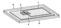
- the semiconductor device 10 of the present disclosure may have a semiconductor chip 2 or the like on the base layer 1 as shown in FIGS. 2F and 3F.
- the semiconductor device 10 of the present disclosure may have the base layer 1 as one of the components on the article S side such as the semiconductor chip 2 that constitutes the semiconductor device.
- the semiconductor device 10 according to the present disclosure preferably includes the semiconductor chip 2 and the like on the base layer 1.
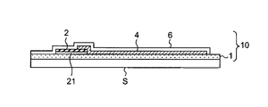
- the semiconductor device 10 of the present disclosure generally further includes a protective film 6 as shown in FIG. 2F and FIG. 3F are a schematic sketch and a schematic cross-sectional view, respectively, showing another example of the structure of the semiconductor device of the present disclosure.
- the semiconductor device 10 when the semiconductor device 10 has the base layer 1 between the semiconductor device 10 and the article S, the base layer 1 is directly formed on the surface of the article S. Further, it is directly fixed (that is, bonded or bonded) to the surface of the article S without any circuit board or adhesive layer interposed therebetween.
- the semiconductor chip 2 or the like included in the semiconductor device achieves the above-described “adhesion” on the surface of the base layer 1 instead of the surface of the article S.
- the semiconductor device 10 includes the base layer 1 between the semiconductor device 10 and the article S as shown in FIGS. 2E and 3E
- the semiconductor device 10 includes the semiconductor chip 2
- the semiconductor chip 2 Is directly mounted on the surface of the underlayer 1, and as a result, an adhesive layer 21 for mounting is interposed between the substrate and the underlayer 1. It is joined.
- the semiconductor chip is not exposed from the surface of the base layer in the thickness direction of the semiconductor chip beyond 1/2 of the height dimension (thickness dimension) of the semiconductor chip (that is, 1 / 2 or more).
- the antenna is exposed from the surface of the base layer in the thickness direction of the antenna at least 1/2 (50 to 100%) of the height (thickness) of the antenna.
- the adhesive 21 may not be interposed, and the base layer 1 may function as an adhesive so that the semiconductor chip 2 is directly fixed to the surface of the article S.
- the region on the semiconductor chip 2 side of the base layer 1 is an adhesive, and the region on the side opposite to the semiconductor chip 2 of the base layer 1 is a base layer.
- the TFT 3 is directly formed on the surface of the base layer 1, and as a result, a circuit board is also pasted between the base layer 1. It is directly bonded and / or bonded to the surface of the underlayer 1 without any interposition.
- the antenna 4 is formed directly on the surface of the base layer 1, and as a result, there is no circuit board or adhesive layer between the base layer and the base layer. Directly bonded or bonded to one surface.
- the wiring 5 is formed directly on the surface of the base layer 1, and as a result, a circuit is formed between the base layer 1. It is directly bonded or bonded to the surface of the underlayer 1 without any substrate or adhesive layer.
- the underlayer 1 that the semiconductor device 10 of the present disclosure may have is a layer for optimizing the surface state of the article.
- the semiconductor device 10 can be fixed to any article.
- the optimization is to reliably avoid electrical conduction of components of the semiconductor device 10 to the article, to reliably avoid moisture permeation from the article to the semiconductor device 10, and to allow the semiconductor chip 2 to be bonded to the article.
- And at least one of the antenna 4 and the wiring 5 can be formed.
- the underlayer 1 is not particularly limited as long as it has a so-called electrical insulating property, and may be, for example, an organic layer such as a polymer layer or an inorganic layer such as a glass layer or a ceramic layer.
- the underlayer 1 is usually a polymer layer.
- the electrical insulating property means, for example, a resistivity of 10 8 ⁇ m or more, preferably 10 8 to 10 17 ⁇ m.
- the polymer constituting the polymer layer include polyester resin (for example, polyethylene terephthalate resin), polyimide resin, polyolefin resin (for example, polyethylene resin, polypropylene resin), polyphenylene sulfide resin, polyvinyl formal resin, polyurethane resin, and polyamideimide resin.
- the thickness of the underlayer 1 is not particularly limited, and may be appropriately determined according to the application of the semiconductor device of the present disclosure (for example, the type of attachment target of the wireless communication device).
- the thickness of the underlayer 1 may be, for example, 0.1 ⁇ m or more, and preferably 10 ⁇ m or more.
- the upper limit of the thickness of the underlayer 1 is not particularly limited, and the thickness is usually less than 100 ⁇ m, preferably 50 ⁇ m or less.
- the semiconductor chip 2 is a semiconductor element mounted on the article S or the underlying layer 1 and is an electronic device called a semiconductor integrated circuit.
- a semiconductor integrated circuit As the semiconductor chip 2, an inorganic semiconductor chip such as a silicon chip or a compound semiconductor is mainly used.
- the semiconductor chip is not particularly limited as long as it is a semiconductor device that can constitute members such as a radio circuit unit, a memory unit, a power supply circuit unit, and a control circuit unit, which will be described later. It may be a component.
- One or more semiconductor chips 2 are used per one semiconductor device, and usually one is used.
- the semiconductor chip is exposed from the surface of the article in the thickness direction of the semiconductor chip by more than half of the height dimension (thickness dimension) of the semiconductor chip.
- the antenna is also preferably exposed from the surface of the article with respect to the thickness direction of the antenna at least 1/2 of the height dimension (thickness dimension) of the antenna.
- the semiconductor chip 2 is exposed at least 1/2 (50 to 100%) in the thickness direction (direction parallel to the direction along the short side of the semiconductor chip 2).
- the antenna 4 is exposed to 1 ⁇ 2 or more in the thickness direction (direction parallel to the short side of the antenna 4).
- the semiconductor chip may be a packaged packaged semiconductor chip or an unpackaged semiconductor bare chip.
- the semiconductor bare chip is advantageous in reducing the size and thickness of the semiconductor device.
- Semiconductor chip (especially silicon chip) 2 is arranged face up (state), that is, with the pads facing upward.
- “upper” means “upward” when the semiconductor chip is placed on the surface of the article or the underlying layer as a substantially horizontal plane.
- the placement is placement, for example, with the surface of the maximum area of the semiconductor chip as the bottom surface.
- the TFT 3 is a switch that allows electricity to flow from the source electrode to the drain electrode by controlling the potential of the gate electrode. If it is a thin film device, it will not specifically limit.
- the TFT may be any known TFT.
- the channel portion (layer) between the source electrode and the drain electrode may be an organic TFT made of an organic semiconductor material, or the channel portion (layer) may be An inorganic TFT made of an inorganic semiconductor material may be used.
- Organic TFTs include, for example, polymer materials (for example, polythiophene or derivatives thereof), low-molecular materials (for example, pentacene, solubilized pentacene), and nanocarbon materials (for example, carbon nanotubes, SiGe nanowires, fullerenes, modified fullerenes). ), An inorganic-organic mixed material (for example, a composite system of (C 6 H 5 C 2 H 4 NH 3 ) and SnI 4 ) or the like.
- the inorganic TFT may be, for example, a silicon TFT such as an amorphous silicon TFT or a polycrystalline silicon TFT.
- the structure of the TFT (especially organic TFT) 3 may be any known structure, for example, so-called bottom gate-bottom contact type, top gate-bottom contact type, bottom gate-top contact type, and top gate-top contact. It may be a mold or the like. From the viewpoint of further reducing the manufacturing cost and further improving the manufacturability of the TFT, the TFT is preferably a bottom gate-top contact type organic TFT.
- the TFT 3 is preferably a printed part from the viewpoint of further reducing the manufacturing cost and further improving the manufacturability of the TFT.
- “TFT 3 is a printed part” means that TFT 3 is a part manufactured by a printing method described later.
- the TFT 3 is preferably an organic TFT from the viewpoint of further improving the safety against peeling from the article of the semiconductor device, further reducing the manufacturing cost, and further improving the manufacturability of the TFT. This is because the organic TFT can be easily manufactured with a simpler structure by a printing method (particularly, an ink jet printing method) as described later, and the security performance is further improved.
- the TFT 3 may be used by one or more per one semiconductor device (particularly a wireless communication device).
- the semiconductor device (especially a wireless communication device) of the present disclosure has a protective film 6 described later, all the TFTs 3 are formed under the protective film 6 (that is, between the article S or the base layer 1 and the protective film 6).
- the wiring 5 is electrically connected to the semiconductor chip 2.
- the antenna 4 is not particularly limited as long as it can receive radio waves from an external reader device and can transmit radio waves based on information and data stored in a semiconductor device (particularly a wireless communication device) to the external reader device.
- the type of the antenna 4 is usually determined by the frequency of the radio wave, and may be, for example, a loop antenna, a spiral antenna, a dipole antenna, a patch antenna, or a dipole antenna bent. In particular, when the frequency of the radio wave is 860 to 2450 MHz, a dipole antenna is preferable.
- the thickness of the antenna 4 is not particularly limited, and may be, for example, 50 nm or more, and is usually 10 nm to 100 ⁇ m.
- the dimensions of the antenna 4 are not particularly limited.
- the total length in the longitudinal direction is usually 10 to 200 mm, preferably 50 to 100 mm, for example, 70 mm, for example, and is perpendicular to the longitudinal direction.
- the total length is usually 5 to 50 mm, preferably 5 to 20 mm. For example, one is 9.5 mm.
- the antenna 4 is preferably a printed part from the viewpoint of further improving the safety against peeling of the semiconductor device from the article, further reducing the manufacturing cost, and further improving the manufacturability of the antenna.
- the antenna 4 being a printed part means that the antenna 4 is a part manufactured by a printing method described later.
- the antenna 4 is not particularly limited as long as it is made of a conductive material.
- the antenna 4 is made of a metal material such as silver (Ag), copper (Cu), nickel (Ni), aluminum (Al), or stainless steel (SUS). It may be.
- the wiring 5 is a wiring for electrically connecting the semiconductor chip 2, the TFT 3 and the antenna 4 to each other.
- the wiring 5 is usually a wiring that electrically connects the semiconductor chip 2 and the antenna 4 (not shown in FIG. 1) or a wiring that electrically connects the TFT 3 and the antenna 4 (in FIG. 1). (Not shown).
- the thickness of the wiring 5 is not particularly limited, and may be, for example, 50 nm or more, and is usually 10 nm to 100 ⁇ m.
- the wiring 5 is preferably a printed part from the viewpoint of further reducing the manufacturing cost and further improving the ease of manufacturing the wiring.
- the wiring 5 being a printed part means that the wiring 5 is a part manufactured by a printing method described later.
- the wiring 5 is not particularly limited as long as it is made of a conductive material.
- the wiring 5 is made of a metal material such as silver (Ag), copper (Cu), nickel (Ni), aluminum (Al), and stainless steel (SUS). It may be.
- the protective film 6 is formed so as to cover at least the semiconductor chip 2 or the like on the surface of the article S or the base layer 1 where the semiconductor chip 2 or the like is formed, and protects and seals the semiconductor chip 2 or the like.
- the protective film 6 is shown as being transparent for the explanation of other members, but is not limited to this and may be opaque.
- the material constituting the protective film 6 is not particularly limited as long as the semiconductor chip 2 and the like can be protected from moisture in the air.
- epoxy resin polyimide (PI) resin, acrylic resin, polyethylene terephthalate (PET) resin, polyethylene naphthalate A phthalate (PEN) resin, a polyphenylene sulfide (PPS) resin, a polyphenylene ether (PPE) resin, a fluororesin, or a composite thereof can be given.
- PI polyimide
- PET polyethylene terephthalate
- PEN polyethylene naphthalate
- PPS polyphenylene sulfide
- PPE polyphenylene ether
- fluororesin or a composite thereof
- fluororesin a fluororesin.
- the thickness of the protective film 6 is not particularly limited, and is preferably in the range of about 0.1 ⁇ m to about 5 ⁇ m, more preferably in the range of about 0.5 ⁇ m to about 2 ⁇ m, for example, about 1 ⁇ m.
- the protective film 6 is preferably a printed part from the viewpoint of further reducing the manufacturing cost and further improving the ease of manufacturing the protective film. That the protective film 6 is a printed part means that the protective film 6 is a part manufactured by a printing method described later.
- the semiconductor device 10 includes one or more components selected from the group consisting of the semiconductor chip 2, the TFT 3, the antenna 4, and the wiring 5, the semiconductor device 10 includes the following steps P1 and Q1.
- Step P1 When the semiconductor device 10 does not include the semiconductor chip 2, it is not necessary to perform Step P1.
- Step Q1 may be performed after step P1, step P1 may be performed during the execution of step Q1, the remaining step Q1 may be performed, or step P1 may be performed after step Q1.
- the semiconductor device 10 includes the semiconductor chip 2 and the TFT 3, a preferable method for manufacturing a semiconductor device from the viewpoints of further improvement in safety against peeling of the semiconductor device from an article, further reduction in manufacturing cost, and further improvement in manufacturability.
- step Q1 after the TFT 3 is formed by the printing method, the semiconductor chip 2 is mounted in step P1, and if desired, the antenna 4 and the wiring 5 are formed by the printing method in step Q1.
- the semiconductor device 10 when the semiconductor device 10 according to the present disclosure includes one or more components selected from the group consisting of the semiconductor chip 2, the TFT 3, the antenna 4, and the wiring 5 on the base layer 1, the semiconductor device 10 Can be produced by a method comprising the following step O and at least one of steps P2 and Q2: Forming the underlayer 1 directly on the surface of the article S; O; Mounting the semiconductor chip 2 directly on the surface of the underlayer 1 P2; Step Q2 in which one or more components selected from the group consisting of the TFT 3, the antenna 4, and the wiring 5 are formed directly on the surface of the underlayer 1 by a printing method.
- step P2 need not be performed.
- step Q2 need not be performed.
- Step O When the semiconductor device 10 includes the semiconductor chip 2 and one or more components selected from the group consisting of the TFT 3, the antenna 4, and the wiring 5 on the base layer 1, the steps of Step O, Step P2, and Step Q2 are performed.
- the implementation order is not particularly limited as long as the semiconductor device of the present disclosure can be manufactured.
- Step P2 and Step Q2 are performed.
- step P2 and step Q2 may be performed in the order of step Q2 after step P2, or after step P2 is performed in the middle of step Q2, and the remaining step Q2 may be performed.
- step P2 may be performed after step Q2.
- the semiconductor device 10 includes the semiconductor chip 2 and the TFT 3 on the base layer 1, the viewpoint of further improving the safety against peeling of the semiconductor device from the article, further reducing the manufacturing cost, and further improving the manufacturability. From this, it forms as follows. That is, after step O is performed and the TFT 3 is formed by the printing method in step Q2, the semiconductor chip 2 is mounted in step P2, and the antenna 4 and the wiring 5 are formed by the printing method in step Q2, if desired.
- the manufacturing method of the semiconductor device is as follows: If desired, first a step R in which the underlayer 1 is formed directly on the surface of the article S; Forming TFT 3 on article S or underlayer 1 by a printing method; S; A step T of mounting the semiconductor chip 2 on the article S or the underlayer 1; and a step U of forming the antenna 4 and the wiring 5 on the article S or the underlayer 1 by a printing method.
- the semiconductor device manufacturing method usually further includes a step V of forming a protective film 6 on the semiconductor chip 2, the TFT 3, the antenna 4 and the wiring 5 mounted or formed on at least one of the article S and the base layer 1 by a printing method. Including.
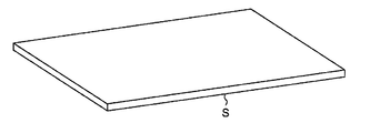
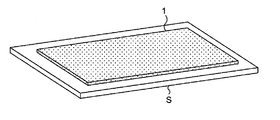
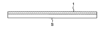
- Step R In Step R, as shown in FIGS. 2A and 3A, after the article S is prepared, if necessary, the underlayer 1 is formed on the article S as shown in FIGS. 2B and 3B.
- 2A and 3A are a schematic sketch and a schematic cross-sectional view, respectively, for explaining an article preparation step in the method of manufacturing a semiconductor device according to the present disclosure.
- FIG. 2B and FIG. 3B are a schematic sketch and a schematic cross-sectional view, respectively, for explaining a base layer manufacturing step in the semiconductor device manufacturing method of the present disclosure.
- the underlayer 1 is formed in FIGS. 2B and 3B, the underlayer 1 does not necessarily have to be formed.
- the underlayer 1 can be manufactured by any coating technique.
- coating techniques include spin coating, wire bar coating, brush coating, spray coating, and gravure roll coating; ink jet printing, screen printing, gravure printing, gravure, etc.
- the printing method include an offset printing method, a reverse offset printing method, and a flexographic printing method.
- the underlayer is preferably manufactured by a coating method.
- the coating liquid used in the coating method for producing the underlayer or the ink used in the printing method may have a desired underlayer material (polymer) dispersed in the solvent, or the polymer in the solvent. It may be dissolved in.
- the solvent is usually dried. At this time, curing may occur if necessary.
- the drying temperature (curing temperature) is usually from 150 to 250 ° C., preferably from 150 to 220 ° C. For example, one is 180 ° C.
- the TFT 3 is formed by a printing method, but does not have to be formed by a printing method, and may be formed by any thin film forming technique.
- the printing method include an inkjet printing method, a screen printing method, a gravure printing method, a gravure offset printing method, a reverse offset printing method, and a flexographic printing method.
- the thin film formation technique include a vacuum film formation method such as a sputtering method, a vapor deposition method, an ion plating method, and a plasma CVD method in addition to the printing method described above. From the viewpoint of further reducing the manufacturing cost and further improving the manufacturability of the TFT 3, the TFT 3 is preferably formed by a printing method (particularly an ink jet method).
- TFT 3 can be formed by a method comprising the following steps: Forming a gate electrode; Forming an insulating layer on the gate electrode; Forming a semiconductor layer on the insulating layer; and forming a source electrode and a drain electrode so that the semiconductor layer is disposed between the source electrode and the drain electrode in plan view.
- Gate electrode formation step The gate electrode is formed at a predetermined position on the circuit board 1.
- gold Au
- silver Ag
- copper Cu
- nickel Ni
- chromium Cr
- cobalt Co
- magnesium Mg
- calcium Ca
- platinum Pt
- Molybdenum Mo
- iron Fe
- zinc Zn
- tin oxide SnO 2
- ITO indium tin oxide
- FTO fluorine-containing tin oxide
- RuO 2 ruthenium oxide
- Conductive oxides such as iridium oxide (IrO 2 ) and platinum oxide (PtO 2 ).
- the formation method of the gate electrode is not particularly limited, and a conventional electrode formation method may be adopted. From the viewpoint of further reducing the manufacturing cost and further improving the manufacturability of the TFT 3, the gate electrode is preferably formed by a printing method (particularly an ink jet printing method). In this embodiment, the gate electrode is formed by forming a silver film with silver nano ink by an inkjet printing method.
- the thickness of the gate electrode is preferably in the range of about 10 nm to about 100 nm, more preferably in the range of about 15 nm to about 50 nm (eg, about 30 nm).
- the ink used in the printing method for forming the gate electrode is an ink (for example, silver nanoink) containing a conductive material such as the above-described metal material or conductive oxide.
- the gate electrode forming ink is usually an ink in which a conductive material is dispersed in a solvent. After forming the gate electrode, the solvent is usually dried. The drying temperature is usually 100 to 200 ° C., preferably 120 to 180 ° C., for example, one is 150 ° C.
- the insulating layer is formed on a gate electrode.
- the insulating layer may be a resin-based or inorganic insulating-based insulating film.
- the resin-based insulating film include films made of epoxy resin, polyimide (PI) resin, polyphenylene ether (PPE) resin, polyphenylene oxide resin (PPO), polyvinyl pyrrolidone (PVP) resin, and the like.
- examples of the inorganic insulating insulating film include, for example, tantalum oxide (Ta 2 O 5 etc.), aluminum oxide (Al 2 O 3 etc.), silicon oxide (SiO 2 etc.), zeolite oxide (ZrO).
- a film made of a dielectric material such as barium titanate (BaTiO 3 ), strontium titanate (SrTiO 3 ), calcium titanate (CaTiO 3 ) can be given.
- a preferred insulating layer is a resin-based insulating film (particularly a polyimide resin film).
- the insulating layer may be formed by a printing method, or a vacuum deposition method, a sputtering method, or the like may be used. Particularly in the case of forming a resin-based insulating film, a coating agent (which may be a resist containing a photosensitive agent) in which a resin material is mixed with a medium is applied to a formation position, followed by drying and heat treatment. By applying and curing, an insulating layer can be formed. On the other hand, in the case of an inorganic insulator system, the insulating layer can be formed by a thin film forming method using a mask (such as sputtering).
- a mask such as sputtering
- the insulating layer is preferably formed by a printing method (particularly an ink jet printing method).
- a polyimide insulating layer is formed by a polyimide solution or a dispersion liquid ink by an ink jet printing method.
- the thickness of the insulating layer is preferably in the range of about 0.1 ⁇ m to about 2 ⁇ m, more preferably in the range of about 0.2 ⁇ m to about 1 ⁇ m (eg, about 0.3 ⁇ m).
- the solvent is usually dried. At this time, curing may occur if necessary.
- the drying temperature (curing temperature) is usually from 150 to 250 ° C., preferably from 150 to 220 ° C. For example, one is 180 ° C.
- a semiconductor layer is formed on an insulating layer.
- the semiconductor layer is preferably an organic semiconductor layer.
- the organic semiconductor material a material having high mobility is preferable, and for example, pentacene can be given.
- the organic semiconductor material that can be used in the present disclosure is not limited thereto, and examples thereof include a high molecular material (for example, polythiophene or a derivative thereof), a low molecular material (for example, pentacene, solubilized pentacene), and a nanocarbon material.
- inorganic-organic mixed materials for example, a composite system of (C 6 H 5 C 2 H 4 NH 3 ) and SnI 4 ) and the like.
- the method for forming the semiconductor layer is not particularly limited, and any method may be used as long as the semiconductor layer can be formed over the insulating layer.
- a printing method for example, in the case of forming a polymer organic semiconductor layer (for example, polythiophene such as poly-3-hexylthiophene (P3HT) or a derivative thereof), a printing method can be suitably used.
- the semiconductor layer can be formed, for example, by spraying a P3HT solution onto the insulating film by an ink jet method and then drying.
- the organic semiconductor layer may be formed by a vapor deposition process.
- the thickness of the semiconductor layer is preferably in the range of about 50 nm to about 150 nm, more preferably in the range of about 80 nm to about 120 nm, for example about 100 nm.
- the solvent is usually dried.
- the drying temperature is usually 150 to 250 ° C., preferably 180 to 220 ° C. For example, one is 200 ° C.
- the source electrode and the drain electrode are formed so that the semiconductor layer is disposed between the source electrode and the drain electrode in plan view.
- the plan view means a plan view when viewed from above in the thickness direction of the TFT.
- “upward” means “upward” when the TFT is formed on the circuit board surface as a substantially horizontal plane.
- the source electrode and the drain electrode may be formed on the semiconductor layer so as to be separated from each other, or may be formed on the insulating layer so as to be in contact with the semiconductor layer. More specifically, the source electrode and the drain electrode may be formed apart from each other on the semiconductor layer.
- the source electrode and the drain electrode are formed on the insulating layer so that the semiconductor layer is disposed between the source electrode and the drain electrode on the insulating layer and is in contact with these electrodes. May be.
- a metal having good conductivity is preferable.
- a metal material such as silver (Ag), copper (Cu), nickel (Ni), aluminum (Al), stainless steel (SUS), etc. Can be used.
- the formation of the source electrode and the drain electrode is not particularly limited, and a conventional electrode forming method may be employed. That is, the source electrode and the drain electrode may be formed by a printing method, or a vacuum evaporation method, a sputtering method, or the like may be used. From the viewpoint of further reducing the manufacturing cost and further improving the manufacturability of the TFT 3, the source electrode and the drain electrode are preferably formed by a printing method (particularly, an ink jet printing method).
- the source electrode and the drain electrode are formed by depositing silver with silver nano-ink by an inkjet printing method.
- the thickness of each of the source and drain electrodes is preferably in the range of about 0.02 ⁇ m to about 10 ⁇ m, more preferably in the range of about 0.03 ⁇ m to about 1 ⁇ m (eg, about 0.1 ⁇ m).
- the ink used in the printing method for forming the source electrode and the drain electrode is an ink containing the above-described metal material (for example, silver nanoink).
- the ink for forming the source electrode and the drain electrode is usually an ink in which a metal material is dispersed in a solvent. After forming the source electrode and the drain electrode, the solvent is usually dried. The drying temperature is usually 100 to 200 ° C., preferably 120 to 180 ° C., for example, one is 150 ° C.
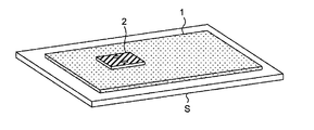
- step T the semiconductor chip 2 is mounted on the base layer 1.
- the semiconductor chip 2 is mounted on the article S.
- the semiconductor chip especially a silicon chip
- commercially available products such as NXP Semiconductors, Impinj, and Alien Technology can be used. Any adhesive may be used as long as it is conventionally used for bonding to a substrate in the field of semiconductor chips.
- 2C and 3C are a schematic sketch and a schematic cross-sectional view, respectively, for explaining a semiconductor chip mounting step in the method for manufacturing a semiconductor device according to the present disclosure.
- the underlayer 1 is formed in FIGS. 2C and 3C, the underlayer 1 is not necessarily formed.
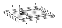
- Step U In Step U, as shown in FIGS. 2D and 3D, the antenna 4 and the wiring 5 (not shown) are formed on the base layer 1 by a printing method.
- the antenna 4 and the wiring 5 are formed on the article S by a printing method.
- the antenna 4 and the wiring 5 are formed by a printing method.
- the antenna 4 and the wiring 5 do not have to be formed by a printing method, and may be formed by any thin film forming technique as with the TFT 3.
- a thin film formation technique for forming the antenna 4 and the wiring 5 for example, a thin film formation technique similar to the thin film formation technique exemplified in the description of the method for forming the TFT 3 can be given.
- the antenna 4 and the wiring 5 are manufactured by a printing method (particularly, an ink jet printing method) from the viewpoint of further improving safety against peeling from the article of the semiconductor device, further reducing manufacturing costs, and further improving manufacturability. Is preferred.
- the ink used in the printing method for forming the antenna 4 and the wiring 5 includes a conductive material such as silver (Ag), copper (Cu), nickel (Ni), aluminum (Al), and stainless steel (SUS). Ink (for example, silver nano ink).
- the ink for forming the antenna 4 and the wiring 5 is usually an ink in which a conductive material is dispersed in a solvent. After the antenna 4 and the wiring 5 are formed, the solvent is usually dried.
- the drying temperature is usually 100 to 200 ° C., preferably 120 to 180 ° C., for example, one is 150 ° C.
- FIG. 3D are a schematic sketch and a schematic cross-sectional view, respectively, for explaining an antenna and wiring formation step in the method for manufacturing a semiconductor device of the present disclosure.
- the underlayer 1 is formed in FIGS. 2D and 3D, the underlayer 1 does not necessarily have to be formed.
- Step V In step V, as shown in FIGS. 2E and 3E, protection is performed on the semiconductor chip 2, TFT 3 (not shown), antenna 4 and wiring 5 (not shown) mounted or formed on the underlayer 1.
- the film 6 is formed by a printing method.
- a protective film 6 is formed on the semiconductor chip 2, TFT 3 (not shown), antenna 4 and wiring 5 (not shown) mounted or formed on the article S by a printing method.
- Form. 2E and 3E are a schematic sketch and a schematic cross-sectional view, respectively, for explaining a protective film forming step in the manufacturing method of the semiconductor device of the present disclosure.
- the underlayer 1 is formed in FIGS. 2E and 3E, the underlayer 1 is not necessarily formed.
- the formation method of the protective film 6 is not specifically limited, For example, it can form by all the coating methods and printing methods illustrated by description of the base layer 1.
- FIG. From the viewpoint of further improving safety against peeling of the semiconductor device from the article, further reducing the manufacturing cost, and further improving the ease of manufacturing the wiring, the protective film is preferably manufactured by a printing method.
- the ink used in the printing method for manufacturing the protective film is an ink containing a desired polymer.
- the polymer may be dispersed in a solvent, or the polymer may be dissolved in the solvent.
- the solvent is usually dried. At this time, curing may occur if necessary.
- the drying temperature (curing temperature) is usually from 150 to 250 ° C., preferably from 150 to 220 ° C. For example, one is 180 ° C.
- the semiconductor device 10 when the surface of the article S to which the semiconductor device 10 is fixed is made of metal, as shown in FIGS. 4A and 4B, the article S (particularly the metal surface) is used as an antenna. Can be used as Accordingly, when the semiconductor device of the present disclosure is a wireless communication device, the structure of the semiconductor device is simplified. 4A and 4B, the antenna 4 also functions as a wiring 5 for electrically connecting to the surface of the article S. That is, the surface of the article S is electrically connected to the semiconductor device 10 (particularly the semiconductor chip 2). The semiconductor device shown in FIGS.
- 4A and 4B is related to the present disclosure described above except that the surface of the article S is electrically connected to the semiconductor device 10 (particularly, the semiconductor chip 2) by the antenna 4 (or the wiring 5). It is the same as the semiconductor device.
- 4A and 4B are a schematic sketch and a schematic cross-sectional view, respectively, showing another example of the structure of the semiconductor device according to the present disclosure.
- the semiconductor device of the present disclosure is useful as a wireless communication device.
- the wireless communication apparatus of the present disclosure includes so-called RFID tags and IC tags, and is used for distribution management (logistics) in retail industries such as convenience stores and supermarkets, apparel industry, transportation industry, and publishing industry (library). Management), production management, inventory management, location management, history management, etc.
Landscapes
- Engineering & Computer Science (AREA)
- Microelectronics & Electronic Packaging (AREA)
- Computer Hardware Design (AREA)
- Physics & Mathematics (AREA)
- General Physics & Mathematics (AREA)
- Theoretical Computer Science (AREA)
- Thin Film Transistor (AREA)
Abstract
Dans la présente invention, la sécurité lors du détachement d'un dispositif à semi-conducteur d'un article est améliorée et l'omission du travail d'adhérence du dispositif à semi-conducteur à un article est réalisée. L'invention concerne un dispositif à semi-conducteur (10) comprenant un ou plusieurs éléments sélectionnés dans le groupe constitué d'une puce semi-conductrice (2), d'un transistor à couches minces (3), d'une antenne (4) et d'un fil (5). Le ou les composants sont directement fixés sur une surface d'un article S. L'invention concerne également un procédé de fabrication du dispositif à semi-conducteur (10) comprenant un ou plusieurs éléments sélectionnés dans le groupe constitué par la puce semi-conductrice (2), le transistor à couches minces (3), l'antenne (4) et le fil (5). Le procédé de fabrication du dispositif à semi-conducteur comprend au moins l'une des étapes suivantes : étape P1 qui consiste à monter directement la puce semi-conductrice sur une surface d'un article ; et étape Q1 qui consiste à former directement, sur la surface de l'article, un ou plusieurs composants choisis dans le groupe constitué par le transistor en couches minces, l'antenne et le fil, par un procédé d'impression.
Priority Applications (3)
| Application Number | Priority Date | Filing Date | Title |
|---|---|---|---|
| CN201980011562.7A CN111684467A (zh) | 2018-02-13 | 2019-02-04 | 半导体装置及其制造方法 |
| US16/955,772 US20200342282A1 (en) | 2018-02-13 | 2019-02-04 | Semiconductor device and manufacturing method therefor |
| JP2020500394A JPWO2019159727A1 (ja) | 2018-02-13 | 2019-02-04 | 半導体装置およびその製造方法 |
Applications Claiming Priority (2)
| Application Number | Priority Date | Filing Date | Title |
|---|---|---|---|
| JP2018-023042 | 2018-02-13 | ||
| JP2018023042 | 2018-02-13 |
Publications (1)
| Publication Number | Publication Date |
|---|---|
| WO2019159727A1 true WO2019159727A1 (fr) | 2019-08-22 |
Family
ID=67620973
Family Applications (1)
| Application Number | Title | Priority Date | Filing Date |
|---|---|---|---|
| PCT/JP2019/003774 Ceased WO2019159727A1 (fr) | 2018-02-13 | 2019-02-04 | Dispositif à semi-conducteur et son procédé de fabrication |
Country Status (4)
| Country | Link |
|---|---|
| US (1) | US20200342282A1 (fr) |
| JP (1) | JPWO2019159727A1 (fr) |
| CN (1) | CN111684467A (fr) |
| WO (1) | WO2019159727A1 (fr) |
Citations (8)
| Publication number | Priority date | Publication date | Assignee | Title |
|---|---|---|---|---|
| JP2002102310A (ja) * | 2000-10-04 | 2002-04-09 | Dainippon Printing Co Ltd | 非接触データキャリア付き薬品パッケージと薬品説明文書および薬品情報の利用方法 |
| JP2004302435A (ja) * | 2003-03-14 | 2004-10-28 | Seiko Epson Corp | 表示装置および電子機器 |
| JP2005092106A (ja) * | 2003-09-19 | 2005-04-07 | Sharp Corp | 平面表示装置、及び平面表示装置もしくはこれを組み込んだ製品の製造情報管理システム |
| JP2006091150A (ja) * | 2004-09-21 | 2006-04-06 | Sharp Corp | ガラス基板、ガラス基板の製造方法、表示パネル、および表示装置 |
| JP2007096276A (ja) * | 2005-08-31 | 2007-04-12 | Semiconductor Energy Lab Co Ltd | 半導体装置及びその作製方法 |
| WO2009084125A1 (fr) * | 2007-12-27 | 2009-07-09 | Sharp Kabushiki Kaisha | Procédé de fabrication de dispositif à semiconducteur et dispositif à semiconducteur |
| JP2010001074A (ja) * | 2008-05-20 | 2010-01-07 | Toyo Seikan Kaisha Ltd | Icタグ付き金属蓋及び金属容器 |
| JP2013156922A (ja) * | 2012-01-31 | 2013-08-15 | Yamagata Univ | Rfidラベル |
Family Cites Families (3)
| Publication number | Priority date | Publication date | Assignee | Title |
|---|---|---|---|---|
| US7768405B2 (en) * | 2003-12-12 | 2010-08-03 | Semiconductor Energy Laboratory Co., Ltd | Semiconductor device and manufacturing method thereof |
| WO2009142146A1 (fr) * | 2008-05-20 | 2009-11-26 | 東洋製罐株式会社 | Couvercle métallique doté d’une étiquette à circuit intégré et récipient métallique |
| CN102395986A (zh) * | 2009-04-14 | 2012-03-28 | 原田秀昭 | 带无线标签物品、无线标签统一读取装置及网络物品管理系统 |
-
2019
- 2019-02-04 WO PCT/JP2019/003774 patent/WO2019159727A1/fr not_active Ceased
- 2019-02-04 CN CN201980011562.7A patent/CN111684467A/zh active Pending
- 2019-02-04 US US16/955,772 patent/US20200342282A1/en not_active Abandoned
- 2019-02-04 JP JP2020500394A patent/JPWO2019159727A1/ja active Pending
Patent Citations (8)
| Publication number | Priority date | Publication date | Assignee | Title |
|---|---|---|---|---|
| JP2002102310A (ja) * | 2000-10-04 | 2002-04-09 | Dainippon Printing Co Ltd | 非接触データキャリア付き薬品パッケージと薬品説明文書および薬品情報の利用方法 |
| JP2004302435A (ja) * | 2003-03-14 | 2004-10-28 | Seiko Epson Corp | 表示装置および電子機器 |
| JP2005092106A (ja) * | 2003-09-19 | 2005-04-07 | Sharp Corp | 平面表示装置、及び平面表示装置もしくはこれを組み込んだ製品の製造情報管理システム |
| JP2006091150A (ja) * | 2004-09-21 | 2006-04-06 | Sharp Corp | ガラス基板、ガラス基板の製造方法、表示パネル、および表示装置 |
| JP2007096276A (ja) * | 2005-08-31 | 2007-04-12 | Semiconductor Energy Lab Co Ltd | 半導体装置及びその作製方法 |
| WO2009084125A1 (fr) * | 2007-12-27 | 2009-07-09 | Sharp Kabushiki Kaisha | Procédé de fabrication de dispositif à semiconducteur et dispositif à semiconducteur |
| JP2010001074A (ja) * | 2008-05-20 | 2010-01-07 | Toyo Seikan Kaisha Ltd | Icタグ付き金属蓋及び金属容器 |
| JP2013156922A (ja) * | 2012-01-31 | 2013-08-15 | Yamagata Univ | Rfidラベル |
Also Published As
| Publication number | Publication date |
|---|---|
| JPWO2019159727A1 (ja) | 2021-02-04 |
| CN111684467A (zh) | 2020-09-18 |
| US20200342282A1 (en) | 2020-10-29 |
Similar Documents
| Publication | Publication Date | Title |
|---|---|---|
| CN101809596B (zh) | Rfid应答器 | |
| CN101896947B (zh) | 包括印刷集成电路的无线器件及其制作和使用方法 | |
| JP4360910B2 (ja) | 電子構成部材、該電子構成部材の回路コンセプト及び製造方法 | |
| JP2004506985A (ja) | 封入された有機電子構成素子、その製造方法および使用 | |
| JP6114677B2 (ja) | プリントされた無線周波数識別(rfid)タグに関する装置および方法 | |
| WO2006052955A2 (fr) | Ensemble comprenant des dispositifs fonctionnels et procede de fabrication correspondant | |
| US20250105499A1 (en) | Method for manufacturing wireless communication device, wireless communication device, and assembly of wireless communication devices | |
| CN101017833A (zh) | 半导体装置 | |
| JP5088544B2 (ja) | 無線icデバイスの製造方法 | |
| CN102132293A (zh) | 混合传感器/通信设备和方法 | |
| JP5151025B2 (ja) | フレキシブル回路基板 | |
| CN101377826B (zh) | 具有整合性基板的射频及/或射频识别电子卷标/装置及其制造与使用方法 | |
| GB2552488A (en) | Field-effect transistor and method for the production thereof | |
| WO2019159727A1 (fr) | Dispositif à semi-conducteur et son procédé de fabrication | |
| US20110253989A1 (en) | Organic electronic circuit | |
| WO2010000806A1 (fr) | Dispositif rfid | |
| US11106965B2 (en) | Radio frequency identification tag and manufacturing method thereof | |
| JP7593107B2 (ja) | 半導体装置用基板、半導体装置用基板の製造方法および無線通信装置の製造方法 | |
| US9601604B2 (en) | Current switching transistor | |
| US20200372317A1 (en) | Wireless communication semiconductor device and manufacturing method therefor | |
| US8144495B2 (en) | Method for programming an electronic circuit and electronic circuit | |
| JP2026063619A (ja) | 半導体装置、その製造方法、それを用いた無線通信装置、真贋判定デバイスおよびセンサ | |
| JP2020013989A (ja) | 改善された歩留まりを示す印刷された電子デバイス |
Legal Events
| Date | Code | Title | Description |
|---|---|---|---|
| 121 | Ep: the epo has been informed by wipo that ep was designated in this application |
Ref document number: 19754106 Country of ref document: EP Kind code of ref document: A1 |
|
| ENP | Entry into the national phase |
Ref document number: 2020500394 Country of ref document: JP Kind code of ref document: A |
|
| NENP | Non-entry into the national phase |
Ref country code: DE |
|
| 122 | Ep: pct application non-entry in european phase |
Ref document number: 19754106 Country of ref document: EP Kind code of ref document: A1 |