WO2019167670A1 - 位相同期回路 - Google Patents
位相同期回路 Download PDFInfo
- Publication number
- WO2019167670A1 WO2019167670A1 PCT/JP2019/005554 JP2019005554W WO2019167670A1 WO 2019167670 A1 WO2019167670 A1 WO 2019167670A1 JP 2019005554 W JP2019005554 W JP 2019005554W WO 2019167670 A1 WO2019167670 A1 WO 2019167670A1
- Authority
- WO
- WIPO (PCT)
- Prior art keywords
- capacitor
- circuit
- current source
- voltage
- phase
- Prior art date
- Legal status (The legal status is an assumption and is not a legal conclusion. Google has not performed a legal analysis and makes no representation as to the accuracy of the status listed.)
- Ceased
Links
Images







Classifications
-
- H—ELECTRICITY
- H03—ELECTRONIC CIRCUITRY
- H03L—AUTOMATIC CONTROL, STARTING, SYNCHRONISATION OR STABILISATION OF GENERATORS OF ELECTRONIC OSCILLATIONS OR PULSES
- H03L7/00—Automatic control of frequency or phase; Synchronisation
- H03L7/06—Automatic control of frequency or phase; Synchronisation using a reference signal applied to a frequency- or phase-locked loop
- H03L7/08—Details of the phase-locked loop
- H03L7/085—Details of the phase-locked loop concerning mainly the frequency- or phase-detection arrangement including the filtering or amplification of its output signal
- H03L7/089—Details of the phase-locked loop concerning mainly the frequency- or phase-detection arrangement including the filtering or amplification of its output signal the phase or frequency detector generating up-down pulses
- H03L7/0891—Details of the phase-locked loop concerning mainly the frequency- or phase-detection arrangement including the filtering or amplification of its output signal the phase or frequency detector generating up-down pulses the up-down pulses controlling source and sink current generators, e.g. a charge pump
- H03L7/0895—Details of the current generators
-
- H—ELECTRICITY
- H03—ELECTRONIC CIRCUITRY
- H03L—AUTOMATIC CONTROL, STARTING, SYNCHRONISATION OR STABILISATION OF GENERATORS OF ELECTRONIC OSCILLATIONS OR PULSES
- H03L7/00—Automatic control of frequency or phase; Synchronisation
- H03L7/06—Automatic control of frequency or phase; Synchronisation using a reference signal applied to a frequency- or phase-locked loop
- H03L7/08—Details of the phase-locked loop
- H03L7/085—Details of the phase-locked loop concerning mainly the frequency- or phase-detection arrangement including the filtering or amplification of its output signal
- H03L7/091—Details of the phase-locked loop concerning mainly the frequency- or phase-detection arrangement including the filtering or amplification of its output signal the phase or frequency detector using a sampling device
-
- H—ELECTRICITY
- H03—ELECTRONIC CIRCUITRY
- H03K—PULSE TECHNIQUE
- H03K5/00—Manipulating of pulses not covered by one of the other main groups of this subclass
- H03K5/22—Circuits having more than one input and one output for comparing pulses or pulse trains with each other according to input signal characteristics, e.g. slope, integral
- H03K5/26—Circuits having more than one input and one output for comparing pulses or pulse trains with each other according to input signal characteristics, e.g. slope, integral the characteristic being duration, interval, position, frequency, or sequence
-
- H—ELECTRICITY
- H03—ELECTRONIC CIRCUITRY
- H03L—AUTOMATIC CONTROL, STARTING, SYNCHRONISATION OR STABILISATION OF GENERATORS OF ELECTRONIC OSCILLATIONS OR PULSES
- H03L7/00—Automatic control of frequency or phase; Synchronisation
- H03L7/06—Automatic control of frequency or phase; Synchronisation using a reference signal applied to a frequency- or phase-locked loop
- H03L7/08—Details of the phase-locked loop
- H03L7/085—Details of the phase-locked loop concerning mainly the frequency- or phase-detection arrangement including the filtering or amplification of its output signal
-
- H—ELECTRICITY
- H03—ELECTRONIC CIRCUITRY
- H03M—CODING; DECODING; CODE CONVERSION IN GENERAL
- H03M3/00—Conversion of analogue values to or from differential modulation
- H03M3/30—Delta-sigma modulation
- H03M3/39—Structural details of delta-sigma modulators, e.g. incremental delta-sigma modulators
- H03M3/412—Structural details of delta-sigma modulators, e.g. incremental delta-sigma modulators characterised by the number of quantisers and their type and resolution
- H03M3/422—Structural details of delta-sigma modulators, e.g. incremental delta-sigma modulators characterised by the number of quantisers and their type and resolution having one quantiser only
- H03M3/424—Structural details of delta-sigma modulators, e.g. incremental delta-sigma modulators characterised by the number of quantisers and their type and resolution having one quantiser only the quantiser being a multiple bit one
- H03M3/426—Structural details of delta-sigma modulators, e.g. incremental delta-sigma modulators characterised by the number of quantisers and their type and resolution having one quantiser only the quantiser being a multiple bit one the quantiser being a successive approximation type analogue/digital converter
-
- H—ELECTRICITY
- H03—ELECTRONIC CIRCUITRY
- H03M—CODING; DECODING; CODE CONVERSION IN GENERAL
- H03M1/00—Analogue/digital conversion; Digital/analogue conversion
- H03M1/12—Analogue/digital converters
- H03M1/34—Analogue value compared with reference values
- H03M1/38—Analogue value compared with reference values sequentially only, e.g. successive approximation type
- H03M1/46—Analogue value compared with reference values sequentially only, e.g. successive approximation type with digital/analogue converter for supplying reference values to converter
- H03M1/466—Analogue value compared with reference values sequentially only, e.g. successive approximation type with digital/analogue converter for supplying reference values to converter using switched capacitors
Definitions
- the present technology relates to a phase synchronization circuit, and more particularly, to a phase synchronization circuit that can reduce power consumption.
- the local oscillator is composed of a PLL circuit, and recently, an ADPLL (All-Digital-PLL) circuit may be used.
- the ADPLL circuit includes a counter circuit that detects an integer phase difference between the DCO frequency signal Fdco and the reference frequency signal Fref, and a TDC circuit (Time-to- (Digital-Converter).
- the counter circuit Since the counter circuit detects an integer phase difference by counting how many Fdcos are input within one cycle of Fref, it must always operate during one cycle of Fref. On the other hand, the TDC circuit only needs to detect the phase difference between the edges of Fref and Fdco. Therefore, the TDC circuit need not always operate during one period of Fref, and can operate intermittently. Since the average current consumption per hour is reduced by performing the intermittent operation, the power can be reduced.
- the TDC circuit detects the phase difference by delaying Fdco by several stages of the inverter circuit and capturing the rising edge of Fref by the latch circuit.
- Non-Patent Document 1 proposes a TDC circuit that improves an increase in power consumption.
- TDC circuit generates a phase difference signal Fref and Fdco in PD (Phase-Detector), configured to obtain a voltage V F and the current charged in capacitor C1 only from the time of the phase difference signal CP (Charge-Pump) Is done.
- PD Phase-Detector
- TDC circuit after obtaining the voltage V F, and generates a voltage V RAMP with current charge from the CP to the capacitor C2, with SS-ADC (Single-Slope ADC ), cross voltage V F and the voltage V RAMP It is configured to count the number of Fdco pulses up to (count number: n). Since the capacities C1 and C2 are 1: N, the slopes of the voltage V F and the voltage V RAMP are N: 1, so that n / N is an AD conversion value and a phase difference between Fref and Fdco.
- Non-Patent Document 1 when the phase difference between Fref and Fdco is large, it is necessary that the CP continues to operate over several Fdco clocks before obtaining the voltage V F and the voltage V RAMP . For this reason, the intermittent rate between 1 period of Fref became low, and it was difficult to reduce electric power sufficiently.
- the present technology has been made in view of such a situation, and can reduce power consumption.
- a phase-locked loop includes two capacitors, outputs a comparison result of voltages generated from the two capacitors, a current source that charges the two capacitors with current,
- the first capacitor is disposed between one of the two capacitors and the current source, and is supplied with a phase difference between a first clock having a reference frequency and a second clock having a higher frequency than the first clock.
- a second switch that is arranged between the other of the two capacitors and the current source and to which the second clock is supplied.
- a SAR-ADC that includes two capacitors and outputs a comparison result of voltages generated from the two capacitors, a current source that charges a current to the two capacitors, and the two capacitors
- the first switch is disposed between one of the capacitors and the current source, and is supplied with a phase difference between a first clock having a reference frequency and a second clock having a higher frequency than the first clock.
- a second switch disposed between the other of the two capacitors and the current source and supplied with the second clock.
- FIG. 2 is a circuit diagram illustrating a configuration example of a TDC circuit in FIG. 1. It is a figure explaining operation
- FIG. 8 is a circuit diagram showing a first modification of the TDC circuit of FIG. 7. It is a figure explaining operation
- FIG. 9 is a circuit diagram showing a second modification of the TDC circuit of FIG. 7. It is a figure explaining operation
- First embodiment ADPLL circuit
- Second embodiment wireless communication apparatus
- FIG. 1 is a block diagram illustrating a configuration example of an ADPLL (ALL Digital PLL) circuit as a phase synchronization circuit to which the present technology is applied.
- ADPLL ALL Digital PLL
- the DCO frequency is higher than the reference frequency.
- the digital set frequency data FCW is data used for setting the DCO frequency, and is supplied from a control unit of the apparatus including the ADPLL circuit 1 or the like.
- the ADPLL circuit 1 includes a counter circuit 11, a TDC (Time-to-Digital Counter) circuit 12, a digital arithmetic circuit 13, and a VCO (Voltage Contorolled Oscillator) 14.
- the reference frequency signal Fref is supplied to the counter circuit 11 and the TDC circuit 12.
- the digital set frequency data FCW is supplied to the digital arithmetic circuit 13.
- the counter circuit 11 detects an integer phase difference between the reference frequency signal Fref supplied from the outside and the DCO frequency signal Fdco supplied from the VCO 14, and outputs a signal representing the detected integer phase difference to the digital arithmetic circuit 13.
- the TDC circuit 12 detects a decimal phase difference between the reference frequency signal Fref supplied from the outside and the DCO frequency signal Fdco supplied from the VCO 14, and outputs a signal representing the detected decimal phase difference to the digital arithmetic circuit 13.
- the digital arithmetic circuit 13 compares the signal representing the phase difference supplied from the counter circuit 11 and the TDC circuit 12 with phase information obtained by time integration of the digital set frequency data FCW, and the comparison result is passed through the digital filter. Output to VCO14.
- the VCO 14 outputs a signal having an oscillation frequency corresponding to the comparison result supplied from the digital arithmetic circuit 13 as a DCO frequency signal Fdco to a subsequent stage (not shown).
- the DCO frequency signal Fdco is fed back to the counter circuit 11 and the TDC circuit 12.
- FIG. 2 is a diagram for explaining the operation of the ADPLL circuit.
- the signal waveform of the reference frequency signal Fref, the signal waveform of the DCO frequency signal Fdco, the integer phase detected by the counter circuit 11, and the decimal phase detected by the TDC circuit 12 are shown in order from the top. Further, an integer phase + decimal phase value for which phase comparison is performed in the digital arithmetic circuit 13 and an integer multiple of the digital set frequency data FCW are shown.
- the digital arithmetic circuit 13 compares the phase of the integer phase + the decimal phase “0” and the integer multiple “0” of the digital set frequency data FCW.
- the digital arithmetic circuit 13 compares the phase of the integer phase + the decimal phase “3.2” and the integer multiple “3.2” of the digital set frequency data FCW.
- the digital arithmetic circuit 13 compares the phase of the integer phase + the decimal phase “6.4” and the integer multiple “6.4” of the digital set frequency data FCW.
- FIG. 3 is a diagram illustrating a conventional TDC circuit for comparison with the present technology.
- the TDC circuit shown in FIG. 3 includes a PD (Phase Locked Loop) 21, a CP (Charge Pump) 22, and an SS-ADC (Single-Slope ADC) 23.
- PD Phase Locked Loop
- CP Charge Pump
- SS-ADC Single-Slope ADC
- the PD 21 generates a phase difference signal ⁇ F (0 to 2 ⁇ ) between the reference frequency signal Fref and the DCO frequency signal Fdco.
- the CP 22 While the phase difference signal ⁇ F is supplied, the CP 22 charges a capacitor C1 (not shown) provided therein. Due to the current charging by the CP 22, a voltage V F that is a phase difference information voltage generated in the capacitor C 1 is output to the SS-ADC 23.
- the voltage V F output from the capacitor C1 is supplied to the comparator 32.
- the current source 31 charges the capacitor C2.
- a voltage V RAMP that is a period information voltage generated in the capacitor C 2 due to the current charge of the current source 31 is output to the comparator 32.
- the comparator 32 compares the voltage V F and the voltage V RAMP, and outputs the comparison result to the integrator 33.
- the integrator 33 counts the number of pulses of the DCO frequency signal Fdco until the voltage V F and the voltage V RAMP intersect (count number: n (n ⁇ 1)), and outputs the calculation result D out .
- n / N becomes an AD conversion value, and a phase difference between the reference frequency signal Fref and the DCO frequency signal Fdco.
- the PD 21 generates a phase difference signal ⁇ F from the time t2 of the rising edge of the reference frequency signal Fref to the time t3 of the next rising edge of the DCO frequency signal Fdco, and outputs it to the CP 22.
- the CP 22 charges the capacitor C1 while the phase difference signal ⁇ F is supplied, that is, from the time t12 of the rising edge of the phase difference signal ⁇ F to the time t13 of the next rising edge of the DCO frequency signal Fdco. As a result, the voltage V F is generated in the capacitor C1.
- the capacitor C2 is charged by the current from the current source 31, so that the voltage V RAMP is applied to the capacitor C2. Occur.
- the integrator 33 counts the number of pulses (2 ⁇ in the case of FIG. 1) of the DCO frequency signal Fdco (count number: n (n ⁇ 1)) until the voltage V RAMP and the voltage V F match in the comparator 32.
- FIG. 4 is a diagram for explaining how to obtain the decimal phase difference between the reference frequency signal Fref and the DCO frequency signal Fdco.
- the upper part shows an example in which the phase difference signal ⁇ F is ⁇ / 2, the DCO frequency signal Fdco is 2 ⁇ , and the calculation result D out is 1. That is, a value 0.25 obtained by dividing one count of the DCO frequency signal Fdco by 4 becomes the value of the phase difference signal ⁇ F.
- the middle stage shows an example when the phase difference signal ⁇ F is ⁇ , the DCO frequency signal Fdco is 2 ⁇ , and the calculation result D out is 2. That is, a value 0.5 obtained by dividing 2 counts of the DCO frequency signal Fdco by 4 becomes the value of the phase difference signal ⁇ F.
- the lower part shows an example in which the phase difference signal ⁇ F is 2 ⁇ , the DCO frequency signal Fdco is 2 ⁇ , and the calculation result D out is 4. That is, a value 1 obtained by dividing 4 counts of the DCO frequency signal Fdco by 4 is the value of the phase difference signal ⁇ F.
- the CP 22 includes a CP 22, an SS-ADC 23, and a normalization unit 51.
- the range of the arrow at the bottom indicates the configuration of each part, and the PD 21 is omitted.
- CP22 includes a current source 31, switches 41, and a capacitor C F.
- the SS-ADC 23 includes a current source 31, a switch 42, a capacitor C R , a comparator 32, a latch circuit 43, an integrator 33, a latch circuit 44, a latch circuit 45, and an arithmetic unit 46.
- the current source 31 includes transistors M p1 and M p2 , and is shared by the CP 22 and the SS-ADC 23 by switching the switches 41 and 42.
- phase difference signal ⁇ F is supplied, the switch 41 is turned on, and the capacitor C F is charged by the current from the current source 31, whereby the voltage V F generated in the capacitor C F is supplied to the comparator 32. Is done.
- the voltage V RAMP generated in the capacitor C R is supplied to the comparator 32.
- the comparator 32 compares the voltage V F with the voltage V RAMP , and outputs a Stop signal to the latch circuit 43 when the voltage V F matches the voltage V RAMP .
- the latch circuit 43 outputs the enable signal EN to the switch 42 when the Start signal output at the end of the supply of the phase difference signal ⁇ F is supplied.
- the integrator 33 counts the number of pulses of the DCO frequency signal Fdco and outputs the count number to the latch circuits 44 and 45.
- the latch circuit 44 holds the count number (14 in FIG. 6 described later) when the Start signal output at the end of the supply of the phase difference signal ⁇ F is supplied, and outputs it to the computing unit 46 at a predetermined timing. .
- the latch circuit 45 holds the count number (83 in FIG. 6 described later) when the Stop signal output from the comparator 32 is supplied, and outputs it to the computing unit 46 at a predetermined timing.
- Calculator 46 outputs the operation result D out which is the difference between the value supplied from the supplied values and latch circuit 45 from the latch circuit 44 to the normalization unit 51.
- the normalizing unit 51 includes a multiplier 47.
- the multiplier 47 outputs the normalized result DF obtained by multiplying the calculation result Dout supplied from the calculator 46 by 1/70 to the subsequent stage.
- FIG. 6 is a diagram for explaining the operation of the TDC circuit of FIG.
- phase difference signal ⁇ F is supplied from time t51 of the rising edge of Fref
- the capacitor C F is charged by the current from the current source 31, and the voltage V F is generated in the capacitor C F.
- the integrator 33 counts the number of pulses of the DCO frequency signal Fdco from the start of the DCO frequency signal Fdco and continues to output the count number to the latch circuits 44 and 45.
- the latch circuit 44 holds the count value (14) at the time t52 of the rising edge of the enable signal EN by the Start signal output at the end of the supply of the phase difference signal ⁇ F.
- the comparator 32 compares the voltage V F and the voltage V RAMP, the time t61 when the voltage V F and the voltage V RAMP matches, the Stop signal, and outputs the latch circuit 45.
- the latch circuit 45 holds the count value (83) at time t61.
- the computing unit 46 outputs the computation result D out (69), which is the difference between the value (14) supplied from the latch circuit 44 and the value (83) supplied from the latch circuit 45, to the normalization unit 51.
- the multiplier 47 outputs the normalized result D F (69/70) obtained by multiplying the calculation result D out (69) supplied from the calculator 46 by 1/70 to the subsequent stage.
- FIG. 7 is a circuit diagram showing a configuration example of the TDC circuit of FIG.
- the current source 111 charges the capacitor 131-1 which is one of the two capacities of the SAR_ADC 114 through the switch 113-1. Further, the current source 111 charges the capacitor 131-2 which is the other of the two capacities of the SAR_ADC 114 via the switch 113-2.
- the PD 112 includes a flip-flop circuit.
- the PD 112 generates a phase difference signal ⁇ F between the reference frequency signal Fref and the DCO frequency signal Fdco.
- the PD 112 outputs the generated phase difference signal ⁇ F to the switch 113-1.
- the switch 113-1 is turned on only while the phase difference signal ⁇ F is supplied.
- the switch 113-1 is on, the current from the current source 111 is charged in the capacitor 131-1, and the voltage V F is generated in the capacitor 131-1.
- the DCO frequency signal Fdco is supplied to the switch 113-2 for one cycle (one clock).
- the switch 113-2 is turned on for one cycle (one clock) of the DCO frequency signal Fdco.
- the SAR_ADC 114 outputs an AD conversion result based on a comparison result between the voltage V F generated in the capacitor 131-1 and the voltage V RAMP generated in the capacitor 131-2.
- the SAR_ADC 114 includes a comparator 121, a SAR logic circuit 122, a capacitor 131-1, a capacitor 131-2, an inverter 132-1, and an inverter 132-2.
- the comparator 121 compares the voltage V F / voltage V RAMP and outputs the comparison result (H / L) to the SAR logic circuit 122.
- the SAR logic circuit 122 calculates the comparison result supplied from the comparator 121 and outputs the calculation result to the outside (not shown).
- the SAR logic circuit 122 controls H / L of the capacitors 131-1 and 131-2 by controlling the inverters 132-1 and 132-2.
- the capacitance of the capacitor 131-1 is C1
- the inverter 132-1 controls H / L of the capacitor 131-1 based on the control of the SAR logic circuit 122.
- Inverter 132-2 controls H / L of the capacity of capacitor 131-2 based on the control of SAR logic circuit 122.
- the set of the capacitor 131-1 and the inverter 132-1 and the set of the capacitor 131-2 and the inverter 132-2 are not limited to one, but may be composed of a plurality.
- the ratio of the capacitance of the set of capacitor 131-1 and inverter 132-1 and the set of capacitor 131-2 and inverter 132-2 is 1: 1.
- FIG. 8 is a diagram for explaining the operation of the TDC circuit of FIG.
- phase difference signal ⁇ F is supplied from the time T1 of the rising edge of the reference frequency signal Fref
- the switch 113-1 is turned on.
- the current from the current source 111 is charged in the capacitor 131-1, and the voltage V F is generated in the capacitor 131-1.
- the switch 113-2 is turned on.
- the current from the current source 111 is charged in the capacitor 131-2, and the voltage V RAMP is generated in the capacitor 131-2.
- the SAR logic circuit 122 controls the inverters 132-1 and 132-2, thereby controlling the H / L of the capacitors 131-1 and 131-2.
- the voltage V F and the voltage V RAMP are sequentially compared in the comparator 121 just by generating the voltage once, and the comparison result is, for example, H, L, H, L, L, H,. ⁇
- the output is as follows.
- the central value of the voltage V F and the voltage V RAMP is the common-mode input voltage (arbitrary) of the comparator.
- the capacitance ratio of the capacitors 131-1 and 131-2 is 1: 1, and the SAR-ADC is used.
- the operation for obtaining the full-scale voltage at the time of AD conversion corresponding to the conventional voltage V RAMP only needs to operate the current source for one cycle (one clock) of the DCO frequency signal Fdco. Therefore, a high intermittent rate can be obtained with respect to the cycle of the reference frequency signal Fref, and the intermittent rate does not depend on the magnitude of the phase difference between the reference frequency signal Fref and the DCO frequency signal Fdco.
- the current source is operated by one clock of the DCO frequency signal Fdco, but any number of clocks may be used as long as it is one clock or more.
- the TDC circuit of the present technology is superior from the viewpoint of being able to operate with lower power than the conventional TDC circuit.
- FIG. 9 is a circuit diagram showing a first modification of the TDC circuit of FIG.
- TDC circuit 12 of FIG. 7 differs from the TDC circuit 12 of FIG. 7 in that current sources 161-1 and 161-2 are added instead of the current source 111.
- Current sources 161-1 and 161-2 have a current mirror ratio of 1: 1, and charge current to capacitors 131-1 and 131-2, respectively.
- FIG. 10 is a diagram for explaining the operation of the TDC circuit of FIG.
- phase difference signal ⁇ F is supplied from the time T11 of the rising edge of the reference frequency signal Fref
- the switch 113-1 is turned on.
- the current from the current source 161-1 is charged in the capacitor 131-1, and the voltage V F is generated in the capacitor 131-1.
- the switch 113-2 is turned on.
- the current from the current source 161-2 is charged in the capacitor 131-2, and the voltage V RAMP is generated in the capacitor 131-2.
- FIG. 11 is a circuit diagram showing a second modification of the TDC circuit of FIG.
- the TDC circuit 12 of FIG. 11 has a point that the capacitances of the capacitors 131-1 and 131-2 are 1: N, and a point that current sources 181-1 and 181-2 are added instead of the current source 111. Different from the TDC circuit 12 of FIG. Since the other configuration is basically the same as the configuration of FIG. 7, the description thereof is omitted.
- FIG. 12 is a diagram for explaining the operation of the TDC circuit of FIG.
- phase difference signal ⁇ F is supplied from the time T21 of the rising edge of the reference frequency signal Fref
- the switch 113-1 is turned on.
- the current from the current source 181-1 is charged in the capacitor 131-1, and the voltage V F is generated in the capacitor 131-1.
- the switch 113-2 is turned on.
- the current from the current source 181-2 is charged in the capacitor 131-2, and the voltage V RAMP is generated in the capacitor 131-2.
- the current charge time from the current source can be shortened, so that the intermittent rate can be improved and the power can be reduced.
- the phase synchronization circuit of the present technology is used in, for example, a high-frequency wireless communication device.
- FIG. 13 is a block diagram illustrating a configuration example of the wireless communication apparatus 200 including the ADPLL circuit 1.
- the wireless communication device 200 includes an ADPLL circuit 1, a modulation unit 201, a transmission mixer 202, a reference signal oscillator 203, a reception mixer 204, and a demodulation unit 205.
- the ADPLL circuit 1 outputs a first local signal and a second local signal having desired frequencies to the transmission mixer 202 and the reception mixer 204 based on the reference signal output from the reference signal oscillator 203, respectively.
- the reference signal oscillator 203 is configured using, for example, a crystal resonator.
- the transmission mixer 202 is supplied with the baseband transmission signal modulated by the modulation unit 400 and the first local signal output by the ADPLL circuit 1.
- the transmission mixer 202 performs up-conversion based on the supplied transmission signal and the first local signal, and converts the baseband transmission signal (BB transmission signal) into a high-frequency transmission signal (RF transmission signal).
- the high-frequency transmission signal is transmitted via an antenna not shown in FIG.
- the present technology is not limited to the wireless communication device, and can be applied to an RF circuit or the like.
- Embodiments of the present technology are not limited to the above-described embodiments, and various modifications can be made without departing from the gist of the present technology.
- a SAR-ADC that includes two capacitors and outputs a comparison result of voltages generated from the two capacitors;
- a phase difference between a first clock having a reference frequency and a second clock having a higher frequency than the first clock is provided between one of the two capacitors and the current source.
- a phase locked loop circuit comprising: a second switch disposed between the other of the two capacitors and the current source and supplied with the second clock.
- the current source charges the one capacitor with a current for a time corresponding to the phase difference based on the operation of the first switch, and the second clock based on the operation of the second switch.
- the phase-locked loop according to (1) wherein a current is charged to the other capacitor for a time corresponding to.
- (3) The phase synchronization circuit according to (2), wherein the time corresponding to the second clock is a time of one clock cycle or more.
- (4) The phase according to any one of (1) to (3), wherein the one capacitor generates a voltage according to the phase difference, and the other capacitor generates a voltage according to the second clock. Synchronous circuit.
- capacitance is 1: 1, The phase synchronous circuit as described in said (4).
- (6) The phase synchronization circuit according to (4), wherein the current source includes a first current source that charges current to the one capacitor and a second current source that charges current to the other capacitor.
- the other capacity is N times the one capacity,
- ADPLL circuit 11 counter circuit, 12 TDC circuit, 13 digital arithmetic circuit, 14 VCO, 111 current source, 112 PD, 113-1 and 113-2 switch, 114 SAR_ADC, 121 comparator, 122 SAR_ logic circuit, 131 -1 and 131-2 capacitors, 132-1 and 132-2 inverters, 161-1 and 161-2 current sources, 181-1 and 181-2 current sources, 200 wireless communication devices, 201 modulation units, 202 transmission mixers, 203 Reference signal oscillator, 204 reception mixer, 205 demodulator
Landscapes
- Engineering & Computer Science (AREA)
- Theoretical Computer Science (AREA)
- Physics & Mathematics (AREA)
- Nonlinear Science (AREA)
- Stabilization Of Oscillater, Synchronisation, Frequency Synthesizers (AREA)
- Manipulation Of Pulses (AREA)
- Analogue/Digital Conversion (AREA)
Abstract
本技術は、消費電力を低減することができるようにする位相同期回路に関する。 2つのキャパシタを含み、2つのキャパシタから発生した電圧の比較結果を出力するSAR-ADCと、2つのキャパシタに電流をチャージする電流源と、2つのキャパシタのうちの一方のキャパシタと電流源の間に配置され、基準周波数の第1のクロックと第1のクロックより高い周波数である第2のクロックとの位相差が供給される第1のスイッチと、2つのキャパシタのうちの他方のキャパシタと電流源の間に配置され、第2のクロックが供給される第2のスイッチとを備える。本開示は、例えば、無線通信装置に適用することができる。
Description
本技術は、位相同期回路に関し、特に、消費電力を低減することができるようにした位相同期回路に関する。
今後到来するIoT時代へ向けてLSIの低電力化が要求されている。LSIに搭載されるアナログブロックの消費電力のうち、局部発振器の消費電力は、大きな割合を占める。局部発振器は、PLL回路で構成され、最近ではADPLL(All-Digital-PLL)回路が用いられる場合がある。
ADPLL回路はデジタル設定周波数データFCW(frequency command word)と外部からの基準周波数から、DCO周波数を、DCO周波数=FCW×基準周波数の関係を満足するように生成する。DCO周波数と基準周波数の比をFCWに合わせるため、ADPLL回路は、DCO周波数信号Fdcoと基準周波数信号Frefの整数位相差を検知するカウンタ回路と、小数位相差を検知するTDC回路(Time-to-Digital-Converter)を有する。
カウンタ回路は、Frefの1周期内にFdcoが何周期入力されるかをカウントすることで整数位相差を検知するので、Frefの1周期の間、常時動作していなければならない。これに対し、TDC回路はFrefとFdcoのエッジの位相差を検出すれば良いので、Frefの1周期の間、常時動作し続ける必要はなく、間欠動作することが可能である。間欠動作を行うことによって時間あたりの平均消費電流が小さくなるため、低電力化を図ることができる。
TDC回路はFdcoをインバータ回路数段で遅延させ、Frefの立ち上がりエッジをラッチ回路で捕えることで位相差を検出する。この構成はシンプルであるが、FrefとFdcoの位相差が大きいときに遅延を生成するために多数のインバータ回路を動作させる必要があり、消費電流の増加を招くため、低電力動作が難しい。
そこで、非特許文献1には、消費電力の増加を改善するようにしたTDC回路が提案されている。TDC回路は、PD(Phase-Detector)でFrefとFdcoの位相差信号を生成し、位相差信号の時間だけCP(Charge-Pump)から容量C1に電流チャージして電圧VFを得るように構成される。
また、TDC回路は、電圧VFを得た後、CPから容量C2に電流チャージして電圧VRAMPを生成し、SS-ADC(Single-Slope ADC)で、電圧VFと電圧VRAMPが交差するまでのFdcoのパルス数をカウント(カウント数:n)するように構成される。容量C1と容量C2が1:Nのため、電圧VFと電圧VRAMPの傾きは、N:1となるので、n/NがAD変換値となり、FrefとFdcoの位相差になる。
Somnath Kundu, Bongjin Kim, Chris H. Kim、"19.2 A 0.2-to-1.45GHz Subsampling Fractional-N All-Digital MDLL with Zero-Offset Aperture PD-Based Spur Cancellation and In-Situ Timing Mismatch Detection"、2016 IEEE International Solid-State Circuits Conference、February 3, 2016、[online][平成30年1月25日検索]、インターネット〈URL:http://www.ee.umn.edu/groups/VLSIresearch/papers/2016/ISSCC16_MDLL.pdf〉
しかしながら、非特許文献1の提案では、FrefとFdcoの位相差が大きいとき、電圧VFと電圧VRAMPを得るまでにFdco数クロックに渡ってCPが動作し続けることが必要であった。このため、Fref1周期間における間欠率が低くなり、十分な低電力化をすることが困難であった。
本技術は、このような状況に鑑みてなされたものであり、消費電力を低減することができるものである。
本技術の一側面の位相同期回路は、2つの容量を含み、前記2つの容量から発生した電圧の比較結果を出力するSAR-ADCと、前記2つの容量に電流をチャージする電流源と、前記2つの容量のうちの一方の容量と前記電流源の間に配置され、基準周波数の第1のクロックと前記第1のクロックより高い周波数である第2のクロックとの位相差が供給される第1のスイッチと、前記2つの容量のうちの他方の容量と前記電流源の間に配置され、前記第2のクロックが供給される第2のスイッチとを備える。
本技術の一側面においては、2つの容量を含み、前記2つの容量から発生した電圧の比較結果を出力するSAR-ADCと、前記2つの容量に電流をチャージする電流源と、前記2つの容量のうちの一方の容量と前記電流源の間に配置され、基準周波数の第1のクロックと前記第1のクロックより高い周波数である第2のクロックとの位相差が供給される第1のスイッチと、前記2つの容量のうちの他方の容量と前記電流源の間に配置され、前記第2のクロックが供給される第2のスイッチとが備えられる。
本技術によれば、消費電力を低減することができる。
なお、本明細書に記載された効果は、あくまで例示であり、本技術の効果は、本明細書に記載された効果に限定されるものではなく、付加的な効果があってもよい。
以下、本開示を実施するための形態(以下実施の形態とする)について説明する。説明は以下の順序で行う。
1.第1の実施の形態(ADPLL回路)
2.第2の実施の形態(無線通信装置)
1.第1の実施の形態(ADPLL回路)
2.第2の実施の形態(無線通信装置)
< 1.第1の実施の形態 >
<本技術のADPLL回路の構成例>
図1は、本技術を適用した位相同期回路としてのADPLL(ALL Digital PLL)回路の構成例を示すブロック図である。
<本技術のADPLL回路の構成例>
図1は、本技術を適用した位相同期回路としてのADPLL(ALL Digital PLL)回路の構成例を示すブロック図である。
図1に示されるADPLL回路1は、デジタル設定周波数データFCW(frequency command word)と外部からの基準周波数から、DCO(DigitalControledOscrator)周波数=FCW×基準周波数の関係を満足するDCO周波数を生成する。DCO周波数は、基準周波数よりも高い周波数である。デジタル設定周波数データFCWは、DCO周波数を設定するために用いられるデータであり、ADPLL回路1を含む装置の制御部などから供給される。
ADPLL回路1は、カウンタ回路11、TDC(Time to Digital Counter)回路12、デジタル演算回路13、およびVCO(Voltage Contorolled Oscillator)14から構成される。
基準周波数信号Frefは、カウンタ回路11とTDC回路12に供給される。デジタル設定周波数データFCWは、デジタル演算回路13に供給される。
カウンタ回路11は、外部から供給された基準周波数信号Frefと、VCO14から供給されたDCO周波数信号Fdcoの整数位相差を検知し、検知した整数位相差を表す信号をデジタル演算回路13に出力する。
TDC回路12は、外部から供給された基準周波数信号Frefと、VCO14から供給されたDCO周波数信号Fdcoの小数位相差を検知し、検知した小数位相差を表す信号をデジタル演算回路13に出力する。
デジタル演算回路13は、カウンタ回路11とTDC回路12から供給された位相差を表す信号を、デジタル設定周波数データFCWを時間積分して得られた位相情報と比較し、比較結果を、デジタルフィルタを通してVCO14に出力する。
VCO14は、デジタル演算回路13から供給された比較結果に応じた発振周波数の信号を、DCO周波数信号Fdcoとして、図示せぬ後段に出力する。DCO周波数信号Fdcoは、カウンタ回路11とTDC回路12にフィードバックされる。
<ADPLL回路の動作例>
図2は、ADPLL回路の動作を説明する図である。
図2は、ADPLL回路の動作を説明する図である。
図2においては、デジタル設定周波数データFCW=3.2の場合の例が示されている。上から順に、基準周波数信号Frefの信号波形、DCO周波数信号Fdcoの信号波形、カウンタ回路11において検知される整数位相、TDC回路12において検知される小数位相が示されている。また、デジタル演算回路13において位相比較が行われる整数位相+小数位相の値とデジタル設定周波数データFCWの整数倍の値が示されている。
基準周波数信号Frefの1つ目の立ち上がりエッジ付近では、DCO周波数信号Fdcoの整数位相は0であり、小数位相も0である。したがって、デジタル演算回路13において、整数位相+小数位相「0」と、デジタル設定周波数データFCWの整数倍「0」の位相比較が行われる。
基準周波数信号Frefの2つ目の立ち上がりエッジ付近では、DCO周波数信号Fdcoの整数位相は3であり、小数位相は0.2である。したがって、デジタル演算回路13において、整数位相+小数位相「3.2」と、デジタル設定周波数データFCWの整数倍「3.2」の位相比較が行われる。
基準周波数信号Frefの3つ目の立ち上がりエッジ付近では、DCO周波数信号Fdcoの整数位相は6であり、小数位相は0.4である。したがって、デジタル演算回路13において、整数位相+小数位相「6.4」と、デジタル設定周波数データFCWの整数倍「6.4」の位相比較が行われる。
なお、立ち上がりエッジの4つ目以降の処理も同様に行われるが、繰り返しになるので、説明を省略する。
<本技術と比較するための従来例の説明>
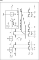
図3は、本技術と比較するための従来のTDC回路について説明する図である。
図3は、本技術と比較するための従来のTDC回路について説明する図である。
図3に示されるTDC回路は、PD(Phase Locked Loop)21、CP(Charge Pump)22、およびSS-ADC(Single-Slope ADC)23で構成される。
PD21は、基準周波数信号FrefとDCO周波数信号Fdcoの位相差信号ΦF(0乃至2π)を生成する。
CP22は、位相差信号ΦFが供給される間、内部に設けられた図示せぬ容量C1に電流チャージする。CP22による電流チャージにより、容量C1に発生した位相差情報電圧である電圧VFがSS-ADC23に出力される。
SS-ADC23は、容量C2(C1:C2=1:N(N≧2))、電流源31、比較器32、および積分器33から構成される。容量C1から出力された電圧VFは、比較器32に供給される。
電流源31は、容量C2に電流チャージする。電流源31の電流チャージにより、容量C2に発生した周期情報電圧である電圧VRAMPが比較器32に出力される。
比較器32は、電圧VFと電圧VRAMPを比較し、比較結果を積分器33に出力する。
積分器33は、電圧VFと電圧VRAMPが交差するまでのDCO周波数信号Fdcoのパルス数をカウント(カウント数:n(n≧1))し、演算結果Doutを出力する。
容量C1と容量C2が1:Nのため、電圧VFと電圧VRAMPの傾きは、N:1となる。n/NがAD変換値となり、基準周波数信号FrefとDCO周波数信号Fdcoの位相差になる。
図3において、構成図の下には、位相差信号ΦFの信号波形、DCO周波数信号Fdcoの信号波形、基準周波数信号Frefの信号波形、容量C1に発生する電圧VFのSlope、および容量C2に発生する電圧VRAMPのSlope(Slope ratio N:1)が示されている。
TDC回路の動作について説明する。PD21は、基準周波数信号Frefの立ち上がりエッジの時刻t2からDCO周波数信号Fdcoの次の立ち上がりエッジの時刻t3までの時間、位相差信号ΦFを生成し、CP22に出力する。
CP22は、位相差信号ΦFが供給される間、すなわち、位相差信号ΦFの立ち上がりエッジの時刻t12からDCO周波数信号Fdcoの次の立ち上がりエッジの時刻t13までの間、容量C1に電流チャージすることで、容量C1に電圧VFが発生する。
容量C1への電流チャージ終了後、1周期待機した後のDCO周波数信号Fdcoの立ち上がりエッジの時刻t14に、電流源31からの電流によって容量C2がチャージされることで、容量C2に電圧VRAMPが発生する。
比較器32において電圧VRAMPと電圧VFが一致するまで、積分器33はDCO周波数信号Fdcoのパルス数(図1の場合、2π)をカウント(カウント数:n(n≧1))する。電圧VRAMPと電圧VFが一致したときのDCO周波数信号Fdcoの立ち上がりエッジの時刻t32に、容量C2への電流源31の電流チャージが終了され、積分器33はカウントを終了して、演算結果Doutを出力する。
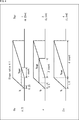
図4は、基準周波数信号FrefとDCO周波数信号Fdcoの小数位相差の求め方を説明する図である。
図4の例においては、Slope ratio 4:1の場合が示されている。
上段には、位相差信号ΦFがπ/2、DCO周波数信号Fdcoが2π、演算結果Doutが1のときの例が示されている。すなわち、DCO周波数信号Fdcoの1カウントを4で割った値0.25が位相差信号ΦFの値となる。
中段には、位相差信号ΦFがπ、DCO周波数信号Fdcoが2π、演算結果Doutが2のときの例が示されている。すなわち、DCO周波数信号Fdcoの2カウントを4で割った値0.5が位相差信号ΦFの値となる。
下段には、位相差信号ΦFが2π、DCO周波数信号Fdcoが2π、演算結果Doutが4のときの例が示されている。すなわち、DCO周波数信号Fdcoの4カウントを4で割った値1が位相差信号ΦFの値となる。
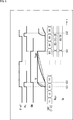
図5は、2つの容量の比が1:N(N=70)、積分器のカウント数n=69の場合の従来のTDC回路の構成例を示す図である。
図5に示されるTDC回路は、CP22、SS-ADC23、および正規化部51で構成される。図5の例において、下部の矢印の範囲が各部の構成を示しており、PD21は省略されている。
CP22は、電流源31、スイッチ41、および容量CFから構成される。
SS-ADC23は、電流源31、スイッチ42、容量CR、比較器32、ラッチ回路43、積分器33、ラッチ回路44、ラッチ回路45、および演算器46から構成される。
電流源31は、トランジスタMp1およびMp2から構成され、スイッチ41および42の切り替えによりCP22とSS-ADC23で共有される。
位相差信号ΦFが供給される間、スイッチ41がオン状態となり、電流源31からの電流によって容量CFがチャージされることで、容量CFに発生した電圧VFが比較器32に供給される。
また、ラッチ回路43からイネーブル信号ENが供給される間、スイッチ42がオン状態となり、電流源31からの電流によって容量CR(CF:CR=1:70)がチャージされることで、容量CRに発生した電圧VRAMPが比較器32に供給される。
比較器32は、電圧VFと電圧VRAMPを比較し、電圧VFと電圧VRAMPが一致した場合、Stop信号を、ラッチ回路43に出力する。
ラッチ回路43は、位相差信号ΦFの供給終了時に出力されたStart信号が供給されると、イネーブル信号ENをスイッチ42に出力する。
積分器33は、DCO周波数信号Fdcoのパルス数をカウントし、カウント数をラッチ回路44および45に出力する。
ラッチ回路44は、位相差信号ΦFの供給終了時に出力されたStart信号が供給されたときのカウント数(後述する図6の14)を保持し、所定のタイミングで、演算器46に出力する。
ラッチ回路45は、比較器32から出力されたStop信号が供給されたときのカウント数(後述する図6の83)を保持し、所定のタイミングで、演算器46に出力する。
演算器46は、ラッチ回路44から供給された値とラッチ回路45から供給された値との差分である演算結果Doutを正規化部51に出力する。
正規化部51は、乗算器47からなる。乗算器47は、演算器46から供給された演算結果Doutに、1/70を乗算して得られた正規化結果DFを後段に出力する。
図6は、図5のTDC回路の動作を説明する図である。
図6においては、上から順に、基準周波数信号Frefの信号波形、位相差信号ΦFの信号波形、イネーブル信号ENの信号波形、容量CFに発生する電圧VFのSlope、および容量CRに発生する電圧VRAMPのSlope(Slope ratio1:70)が示されている。なお、どちらのSlopeも、誤差などの影響により、実線に示されるように実際にはリニアではない。ただし、同じ条件下であるので、電圧の比較の際には、破線に示されるように、誤差などが除去されたリニアのSlopeが用いられる。
また、Slopeの下に、積分器33のカウント値、演算結果Doutの値、および正規化結果DFの値が示されている。
Frefの立ち上がりエッジの時刻t51から位相差信号ΦFが供給される間、電流源31からの電流によって容量CFがチャージされ、容量CFに電圧VFが発生する。積分器33は、DCO周波数信号Fdcoの開始からDCO周波数信号Fdcoのパルス数をカウントし、カウント数を、ラッチ回路44および45に出力し続けている。ラッチ回路44は、位相差信号ΦFの供給終了時に出力されたStart信号によるイネーブル信号ENの立ち上がりエッジの時刻t52のカウントの値(14)を保持する。
比較器32は、電圧VFと電圧VRAMPを比較し、電圧VFと電圧VRAMPが一致したときの時刻t61に、Stop信号を、ラッチ回路45に出力する。ラッチ回路45は、時刻t61のカウントの値(83)を保持する。
演算器46は、ラッチ回路44から供給された値(14)とラッチ回路45から供給された値(83)との差分である演算結果Dout(69)を正規化部51に出力する。
乗算器47は、演算器46から供給された演算結果Dout(69)に、1/70を乗算して得られた正規化結果DF(69/70)を後段に出力する。
以上、従来のTDC回路においては、図5および図6を参照して上述したように、基準周波数信号FrefとDCO周波数信号Fdcoの位相差が大きい場合、電圧VRAMPと電圧VFを得るためにDCO周波数信号Fdco数クロックに渡ってCPまたは電流源を動作し続けることが必要となる。これによって、基準周波数信号Fref1周期における間欠率が低くなって、十分な低電力化ができない。
<本技術のTDC回路>
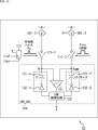
図7は、図1のTDC回路の構成例を示す回路図である。
図7は、図1のTDC回路の構成例を示す回路図である。
図7のTDC回路12は、電流源111、PD112、スイッチ113-1および113-2、並びに、2つの容量を有するSAR(Successive Approximation)_ADC114から構成される。
電流源111は、スイッチ113-1を介して、SAR_ADC114の2つの容量のうちの一方の容量であるキャパシタ131-1に電流チャージする。また、電流源111は、スイッチ113-2を介して、SAR_ADC114の2つの容量うちの他方の容量であるキャパシタ131-2に電流チャージする。
PD112は、フリップフロップ回路からなる。PD112は、基準周波数信号FrefとDCO周波数信号Fdcoの位相差信号ΦFを生成する。PD112は、生成した位相差信号ΦFをスイッチ113-1に出力する。これにより、位相差信号ΦFが供給される間だけスイッチ113-1がオン状態となる。スイッチ113-1がオン状態のとき、電流源111による電流がキャパシタ131-1にチャージされ、キャパシタ131-1に電圧VFが発生する。
電流源111による電流のキャパシタ131-1へのチャージ後、DCO周波数信号Fdcoが1周期(1クロック)分、スイッチ113-2に供給される。これにより、DCO周波数信号Fdcoの1周期(1クロック)分、スイッチ113-2がオン状態となる。スイッチ113-2がオン状態のとき、電流源111による電流がキャパシタ131-2にチャージされ、キャパシタ131-2に電圧VRAMPが発生する。
SAR_ADC114は、キャパシタ131-1に発生した電圧VFとキャパシタ131-2に発生した電圧VRAMPの比較結果に基づくAD変換結果を出力する。
SAR_ADC114は、比較器121、SAR論理回路122、キャパシタ131-1、キャパシタ131-2、インバータ132-1、およびインバータ132-2から構成される。
比較器121は、電圧VF/電圧VRAMPを比較し、比較結果(H/L)をSAR論理回路122に出力する。
SAR論理回路122は、比較器121から供給された比較結果を演算し、演算結果を、図示せぬ外部に出力する。SAR論理回路122は、インバータ132-1および132-2を制御することで、キャパシタ131-1および131-2のH/Lを制御する。
キャパシタ131-1の容量は、C1であり、キャパシタ131-2容量は、C2(C1:C2=1:1)である。
インバータ132-1は、SAR論理回路122の制御に基づいて、キャパシタ131-1のH/Lを制御する。インバータ132-2は、SAR論理回路122の制御に基づいて、キャパシタ131-2の容量のH/Lを制御する。
なお、キャパシタ131-1およびインバータ132-1の組、キャパシタ131-2およびインバータ132-2の組は、1つずつに限らず、複数で構成されてもよい。ただし、キャパシタ131-1およびインバータ132-1の組とキャパシタ131-2およびインバータ132-2の組の容量の比は1:1である。
<TDC回路の動作>
図8は、図7のTDC回路の動作を説明する図である。
図8は、図7のTDC回路の動作を説明する図である。
図8においては、上から順に、基準周波数信号Frefの信号波形、DCO周波数信号Fdcoの信号波形、位相差信号ΦFの信号波形、キャパシタ131-1(C1)に発生する電圧VFのSlope、およびキャパシタ131-2(C2)に発生する電圧VRAMPのSlopeが示されている。
基準周波数信号Frefの立ち上がりエッジの時刻T1から位相差信号ΦFが供給される間、スイッチ113-1がオン状態となる。電流源111による電流が、キャパシタ131-1にチャージされ、キャパシタ131-1に電圧VFが発生する。1周期待機後、次のDCO周波数信号Fdcoの立ち上がりエッジの時刻T3から1周期、DCO周波数信号Fdcoが供給されるので、スイッチ113-2がオン状態となる。電流源111による電流が、キャパシタ131-2にチャージされ、キャパシタ131-2に電圧VRAMPが発生する。
その後、次の立ち上がりエッジの時刻T5から、SAR論理回路122は、インバータ132-1および132-2を制御することで、キャパシタ131-1および131-2のH/Lを制御する。これにより、電圧を1度発生しただけで、比較器121において電圧VFと電圧VRAMPの値が逐次比較され、比較結果が、例えば、H,L,H,L,L,H,・・・というように出力される。
なお、電圧VFと電圧VRAMPの中央の値は、比較器の同相入力電圧(任意)である。
以上のように、本技術においては、キャパシタ131-1および131-2の容量比が1:1であり、また、SAR-ADCが用いられる。これにより、従来の電圧VRAMPに相当するAD変換時のフルスケール電圧を得るための動作は、電流源をDCO周波数信号Fdcoの1周期(1クロック)動作させるのみでよい。したがって、基準周波数信号Frefの周期に対して高い間欠率を得ることが可能であり、基準周波数信号FrefとDCO周波数信号Fdcoの位相差の大きさに間欠率が依存することがない。
ここで、電流源をDCO周波数信号Fdcoの1クロック動作させると説明したが、1クロック以上であれば、何クロックであってもよい。
これに対して、図3乃至図5で上述した従来のTDC回路においては、電圧VRAMPを得るために、電流源を、DCO周波数信号Fdcoの2クロック以上動作させることが必要であった。また、従来のTDC回路では、基準周波数信号FrefとDCO周波数信号Fdcoの位相差が大きい場合には、電圧VRAMPを得るために電流源を動作させる期間が延びてFref1周期における間欠率が下がることがあり得る。したがって、本技術のTDC回路は、従来のTDC回路よりも低電力動作可能となる観点で優位である。
<第1の変形例>
図9は、図7のTDC回路の第1の変形例を示す回路図である。
図9は、図7のTDC回路の第1の変形例を示す回路図である。
図9のTDC回路12は、電流源111の代わりに、電流源161-1および161-2が追加された点が、図7のTDC回路12と異なる。それ以外の構成は、基本的に図7の構成と同様であるため、説明を省略する。
電流源161-1および161-2は、カレントミラー比が1:1であり、キャパシタ131-1および131-2に、それぞれ、電流チャージする。
<TDC回路の動作>
図10は、図9のTDC回路の動作を説明する図である。
図10は、図9のTDC回路の動作を説明する図である。
図10においては、上から順に、基準周波数信号Frefの信号波形、DCO周波数信号Fdcoの信号波形、位相差信号ΦFの信号波形、キャパシタ131-1(C1)に発生する電圧VFのSlope、およびキャパシタ131-2(C2)に発生する電圧VRAMPのSlopeが示されている。
基準周波数信号Frefの立ち上がりエッジの時刻T11から位相差信号ΦFが供給される間、スイッチ113-1がオン状態となる。電流源161-1による電流が、キャパシタ131-1にチャージされ、キャパシタ131-1に電圧VFが発生する。直後のDCO周波数信号Fdcoの立ち上がりエッジの時刻T12から1周期、DCO周波数信号Fdcoが供給されるので、スイッチ113-2がオン状態となる。電流源161-2による電流が、キャパシタ131-2にチャージされ、キャパシタ131-2に電圧VRAMPが発生する。
電圧の発生以降のTDC回路の動作は、図8の例と基本的に同様であるので、その説明は省略される。
以上のように、図9のTDC回路の場合、電圧VRAMPの電流チャージを1周期待つことなく、電圧VFと電圧VRAMPを同時にチャージすることができるので、図7のTDC回路よりも早くAD変換結果が得られる。
<第2の変形例>
図11は、図7のTDC回路の第2の変形例を示す回路図である。
図11は、図7のTDC回路の第2の変形例を示す回路図である。
図11のTDC回路12は、キャパシタ131-1および131-2の容量が1:Nである点と、電流源111の代わりに、電流源181-1および181-2が追加された点が、図7のTDC回路12と異なる。それ以外の構成は、基本的に図7の構成と同様であるため、説明を省略する。
すなわち、電流源181-1および181-2は、カレントミラー比が1:Nであり、それぞれ、容量がC1であるキャパシタ131-1、および容量がC2(=N×C1)であるキャパシタ131-2に電流チャージする。
<TDC回路の動作>
図12は、図11のTDC回路の動作を説明する図である。
図12は、図11のTDC回路の動作を説明する図である。
図12においては、上から順に、基準周波数信号Frefの信号波形、DCO周波数信号Fdcoの信号波形、位相差信号ΦFの信号波形、キャパシタ131-1(C1)に発生する電圧VFのSlope、およびキャパシタ131-2(C2)に発生する電圧VRAMPのSlopeが示されている。
基準周波数信号Frefの立ち上がりエッジの時刻T21から位相差信号ΦFが供給される間、スイッチ113-1がオン状態となる。電流源181-1による電流が、キャパシタ131-1にチャージされ、キャパシタ131-1に電圧VFが発生する。直後のDCO周波数信号Fdcoの立ち上がりエッジの時刻T22から1周期、DCO周波数信号Fdcoが供給されるので、スイッチ113-2がオン状態となる。電流源181-2による電流が、キャパシタ131-2にチャージされ、キャパシタ131-2に電圧VRAMPが発生する。
電圧の発生以降は、図8の例と基本的に同様であるので、その説明は省略される。
以上のように、図11のTDC回路においては、電圧VRAMPの電流チャージを1周期待つことなく、電圧VFと電圧VRAMPを同時にチャージすることができるので、図7のTDC回路の場合よりも早くAD変換結果が得られる。
本技術によれば、電流源からの電流チャージ時間を短くできることで間欠率を向上し、低電力化可能となる。
本技術の位相同期回路は、例えば、高周波の無線通信装置に用いられる。
< 2.第2の実施の形態 >
<無線通信装置の構成例>
図13は、ADPLL回路1を含む無線通信装置200の構成例を示すブロック図である。無線通信装置200は、ADPLL回路1、変調部201、送信ミキサ202、基準信号発振器203、受信ミキサ204、および復調部205から構成される。
<無線通信装置の構成例>
図13は、ADPLL回路1を含む無線通信装置200の構成例を示すブロック図である。無線通信装置200は、ADPLL回路1、変調部201、送信ミキサ202、基準信号発振器203、受信ミキサ204、および復調部205から構成される。
ADPLL回路1は、基準信号発振器203から出力される基準信号に基づいて、所望の周波数の第1局部信号および第2局部信号を、送信ミキサ202および受信ミキサ204にそれぞれ出力する。なお、基準信号発振器203は、例えば水晶振動子を用いて構成される。
送信ミキサ202には、変調部400により変調されたベースバンドの送信信号と、ADPLL回路1により出力された第1局部信号とが供給される。送信ミキサ202は、供給された送信信号と第1局部信号とに基づいてアップコンバートし、ベースバンドの送信信号(BB送信信号)を高周波送信信号(RF送信信号)に変換する。なお、高周波送信信号は、図13に不図示のアンテナを介して送信される。
なお、上記説明においては、無線通信装置に用いる例を説明したが、無線通信装置に限らず、本技術は、RF回路などに適用することができる。
また、本明細書に記載された効果はあくまで例示であって限定されるものでは無く、また他の効果があってもよい。
本技術の実施の形態は、上述した実施の形態に限定されるものではなく、本技術の要旨を逸脱しない範囲において種々の変更が可能である。
以上、添付図面を参照しながら本開示の好適な実施形態について詳細に説明したが、本開示はかかる例に限定されない。本開示の属する技術の分野における通常の知識を有する者であれば、請求の範囲に記載された技術的思想の範疇内において、各種の変更例または修正例に想到し得ることは明らかであり、これらについても、当然に本開示の技術的範囲に属するものと了解される。
なお、本技術は以下のような構成も取ることができる。
(1)
2つの容量を含み、前記2つの容量から発生した電圧の比較結果を出力するSAR-ADCと、
前記2つの容量に電流をチャージする電流源と、
前記2つの容量のうちの一方の容量と前記電流源の間に配置され、基準周波数の第1のクロックと前記第1のクロックより高い周波数である第2のクロックとの位相差が供給される第1のスイッチと、
前記2つの容量のうちの他方の容量と前記電流源の間に配置され、前記第2のクロックが供給される第2のスイッチと
を備える位相同期回路。
(2)
前記電流源は、前記第1のスイッチの動作に基づいて、前記位相差に応じた時間、前記一方の容量に電流をチャージし、前記第2のスイッチの動作に基づいて、前記第2のクロックに応じた時間、前記他方の容量に電流をチャージする
前記(1)に記載の位相同期回路。
(3)
前記第2のクロックに応じた時間は、クロック1周期以上の時間である
前記(2)に記載の位相同期回路。
(4)
前記一方の容量は、前記位相差に応じた電圧を発生させ、前記他方の容量は、前記第2のクロックに応じた電圧を発生させる
前記(1)乃至(3)のいずれかに記載の位相同期回路。
(5)
前記一方の容量と前記他方の容量の比は、1対1である
前記(4)に記載の位相同期回路。
(6)
前記電流源は、前記一方の容量に電流をチャージする第1の電流源と、前記他方の容量に電流をチャージする第2の電流源により構成される
前記(4)に記載の位相同期回路。
(7)
前記他方の容量は、前記一方の容量のN倍の容量であり、
前記第2の電流源は、前記第1の電流源のN倍の電流をチャージする
前記(6)に記載の位相同期回路。
(1)
2つの容量を含み、前記2つの容量から発生した電圧の比較結果を出力するSAR-ADCと、
前記2つの容量に電流をチャージする電流源と、
前記2つの容量のうちの一方の容量と前記電流源の間に配置され、基準周波数の第1のクロックと前記第1のクロックより高い周波数である第2のクロックとの位相差が供給される第1のスイッチと、
前記2つの容量のうちの他方の容量と前記電流源の間に配置され、前記第2のクロックが供給される第2のスイッチと
を備える位相同期回路。
(2)
前記電流源は、前記第1のスイッチの動作に基づいて、前記位相差に応じた時間、前記一方の容量に電流をチャージし、前記第2のスイッチの動作に基づいて、前記第2のクロックに応じた時間、前記他方の容量に電流をチャージする
前記(1)に記載の位相同期回路。
(3)
前記第2のクロックに応じた時間は、クロック1周期以上の時間である
前記(2)に記載の位相同期回路。
(4)
前記一方の容量は、前記位相差に応じた電圧を発生させ、前記他方の容量は、前記第2のクロックに応じた電圧を発生させる
前記(1)乃至(3)のいずれかに記載の位相同期回路。
(5)
前記一方の容量と前記他方の容量の比は、1対1である
前記(4)に記載の位相同期回路。
(6)
前記電流源は、前記一方の容量に電流をチャージする第1の電流源と、前記他方の容量に電流をチャージする第2の電流源により構成される
前記(4)に記載の位相同期回路。
(7)
前記他方の容量は、前記一方の容量のN倍の容量であり、
前記第2の電流源は、前記第1の電流源のN倍の電流をチャージする
前記(6)に記載の位相同期回路。
1 ADPLL回路, 11 カウンタ回路, 12 TDC回路, 13 デジタル演算回路, 14 VCO, 111 電流源, 112 PD, 113-1および113-2 スイッチ, 114 SAR_ADC, 121 比較器, 122 SAR_論理回路, 131-1および131-2 キャパシタ, 132-1および132-2 インバータ, 161-1および161-2 電流源, 181-1および181-2 電流源, 200 無線通信装置, 201 変調部, 202 送信ミキサ, 203 基準信号発振器, 204 受信ミキサ, 205 復調部
Claims (7)
- 2つの容量を含み、前記2つの容量から発生した電圧の比較結果を出力するSAR-ADCと、
前記2つの容量に電流をチャージする電流源と、
前記2つの容量のうちの一方の容量と前記電流源の間に配置され、基準周波数の第1のクロックと前記第1のクロックより高い周波数である第2のクロックとの位相差が供給される第1のスイッチと、
前記2つの容量のうちの他方の容量と前記電流源の間に配置され、前記第2のクロックが供給される第2のスイッチと
を備える位相同期回路。 - 前記電流源は、前記第1のスイッチの動作に基づいて、前記位相差に応じた時間、前記一方の容量に電流をチャージし、前記第2のスイッチの動作に基づいて、前記第2のクロックに応じた時間、前記他方の容量に電流をチャージする
請求項1に記載の位相同期回路。 - 前記第2のクロックに応じた時間は、クロック1周期以上の時間である
請求項2に記載の位相同期回路。 - 前記一方の容量は、前記位相差に応じた電圧を発生させ、前記他方の容量は、前記第2のクロックに応じた電圧を発生させる
請求項2に記載の位相同期回路。 - 前記一方の容量と前記他方の容量の比は、1対1である
請求項4に記載の位相同期回路。 - 前記電流源は、前記一方の容量に電流をチャージする第1の電流源と、前記他方の容量に電流をチャージする第2の電流源により構成される
請求項4に記載の位相同期回路。 - 前記他方の容量は、前記一方の容量のN倍の容量であり、
前記第2の電流源は、前記第1の電流源のN倍の電流をチャージする
請求項6に記載の位相同期回路。
Priority Applications (4)
| Application Number | Priority Date | Filing Date | Title |
|---|---|---|---|
| US16/976,670 US11115031B2 (en) | 2018-03-02 | 2019-02-15 | Phase-locked loop |
| JP2020503392A JP7346379B2 (ja) | 2018-03-02 | 2019-02-15 | 位相同期回路 |
| CN201980015277.2A CN111771332B (zh) | 2018-03-02 | 2019-02-15 | 锁相环电路 |
| EP19761589.1A EP3761509A4 (en) | 2018-03-02 | 2019-02-15 | PHASE LOCK LOOP CIRCUIT |
Applications Claiming Priority (2)
| Application Number | Priority Date | Filing Date | Title |
|---|---|---|---|
| JP2018-037428 | 2018-03-02 | ||
| JP2018037428 | 2018-03-02 |
Publications (1)
| Publication Number | Publication Date |
|---|---|
| WO2019167670A1 true WO2019167670A1 (ja) | 2019-09-06 |
Family
ID=67806097
Family Applications (1)
| Application Number | Title | Priority Date | Filing Date |
|---|---|---|---|
| PCT/JP2019/005554 Ceased WO2019167670A1 (ja) | 2018-03-02 | 2019-02-15 | 位相同期回路 |
Country Status (5)
| Country | Link |
|---|---|
| US (1) | US11115031B2 (ja) |
| EP (1) | EP3761509A4 (ja) |
| JP (1) | JP7346379B2 (ja) |
| CN (1) | CN111771332B (ja) |
| WO (1) | WO2019167670A1 (ja) |
Cited By (1)
| Publication number | Priority date | Publication date | Assignee | Title |
|---|---|---|---|---|
| CN110703246A (zh) * | 2019-10-24 | 2020-01-17 | 中国科学院电子学研究所 | 一种信号同步装置及系统 |
Families Citing this family (1)
| Publication number | Priority date | Publication date | Assignee | Title |
|---|---|---|---|---|
| CN111654281B (zh) * | 2020-06-10 | 2023-08-04 | 上海兆芯集成电路股份有限公司 | 时数转换器 |
Citations (2)
| Publication number | Priority date | Publication date | Assignee | Title |
|---|---|---|---|---|
| JPH09153773A (ja) * | 1995-09-29 | 1997-06-10 | Asahi Kasei Micro Syst Kk | 可変時間遅延回路とその方法 |
| JP2017163546A (ja) * | 2016-03-11 | 2017-09-14 | 株式会社ソシオネクスト | タイミング差異の測定 |
Family Cites Families (11)
| Publication number | Priority date | Publication date | Assignee | Title |
|---|---|---|---|---|
| US5982221A (en) * | 1997-08-13 | 1999-11-09 | Analog Devices, Inc. | Switched current temperature sensor circuit with compounded ΔVBE |
| US6097239A (en) * | 1999-02-10 | 2000-08-01 | Analog Devices, Inc. | Decoupled switched current temperature circuit with compounded ΔV be |
| US7312648B2 (en) * | 2005-06-23 | 2007-12-25 | Himax Technologies, Inc. | Temperature sensor |
| JP5169008B2 (ja) * | 2007-04-27 | 2013-03-27 | 日本電気株式会社 | 電圧制御発振器を内蔵したPLL(PhaseLockedLoop)回路の位相差検出回路 |
| JP5561010B2 (ja) * | 2010-08-09 | 2014-07-30 | 富士通株式会社 | 逐次比較型ad変換器及び逐次比較型ad変換器の動作クロック調整方法 |
| WO2013076797A1 (ja) * | 2011-11-21 | 2013-05-30 | 富士通株式会社 | Adpll |
| US8957712B2 (en) * | 2013-03-15 | 2015-02-17 | Qualcomm Incorporated | Mixed signal TDC with embedded T2V ADC |
| US10177752B2 (en) * | 2014-12-25 | 2019-01-08 | DecaWave, Ltd. | Frequency comparator and early-late detector |
| EP3059857B1 (en) * | 2015-02-17 | 2021-11-03 | Nxp B.V. | Time to digital converter and phase locked loop |
| US9285778B1 (en) * | 2015-08-18 | 2016-03-15 | Cadence Design Systems, Inc. | Time to digital converter with successive approximation architecture |
| EP3139186B1 (en) * | 2015-09-01 | 2018-08-01 | Nxp B.V. | Sensor circuit |
-
2019
- 2019-02-15 CN CN201980015277.2A patent/CN111771332B/zh active Active
- 2019-02-15 WO PCT/JP2019/005554 patent/WO2019167670A1/ja not_active Ceased
- 2019-02-15 EP EP19761589.1A patent/EP3761509A4/en active Pending
- 2019-02-15 US US16/976,670 patent/US11115031B2/en active Active
- 2019-02-15 JP JP2020503392A patent/JP7346379B2/ja active Active
Patent Citations (2)
| Publication number | Priority date | Publication date | Assignee | Title |
|---|---|---|---|---|
| JPH09153773A (ja) * | 1995-09-29 | 1997-06-10 | Asahi Kasei Micro Syst Kk | 可変時間遅延回路とその方法 |
| JP2017163546A (ja) * | 2016-03-11 | 2017-09-14 | 株式会社ソシオネクスト | タイミング差異の測定 |
Non-Patent Citations (2)
| Title |
|---|
| See also references of EP3761509A4 |
| SOMNATH KUNDUBONGJIN KIMCHRIS H. KIM: "19.2 A 0.2-to-1.45 GHz Subsampling Fractional-N All-Digital MDLL with Zero-Offset Aperture PD-Based Spur Cancellation and In-Situ Timing Mismatch Detection", 2016 IEEE INTERNATIONAL SOLID-STATE CIRCUITS CONFERENCE, 3 February 2016 (2016-02-03), Retrieved from the Internet <URL:http://www.ee.umn.edu/groups/VLSIresearch/papers/2016/ISSCC16MDLL.pdf> |
Cited By (1)
| Publication number | Priority date | Publication date | Assignee | Title |
|---|---|---|---|---|
| CN110703246A (zh) * | 2019-10-24 | 2020-01-17 | 中国科学院电子学研究所 | 一种信号同步装置及系统 |
Also Published As
| Publication number | Publication date |
|---|---|
| US20210006255A1 (en) | 2021-01-07 |
| EP3761509A4 (en) | 2021-04-14 |
| JP7346379B2 (ja) | 2023-09-19 |
| CN111771332A (zh) | 2020-10-13 |
| US11115031B2 (en) | 2021-09-07 |
| EP3761509A1 (en) | 2021-01-06 |
| CN111771332B (zh) | 2023-11-21 |
| JPWO2019167670A1 (ja) | 2021-03-04 |
Similar Documents
| Publication | Publication Date | Title |
|---|---|---|
| JP5347534B2 (ja) | 位相比較器、pll回路、及び位相比較器の制御方法 | |
| JP5044434B2 (ja) | 位相同期回路及びこれを用いた受信機 | |
| CN105187055B (zh) | 具有宽带宽的锁相环电路 | |
| US10218364B2 (en) | Time to digital converter, phase difference pulse generator, radio communication device, and radio communication method | |
| JP2011205328A (ja) | 局部発振器 | |
| US20180138899A1 (en) | Systems and methods for phase synchronization of local oscillator paths in oscillator-operated circuits | |
| KR102123901B1 (ko) | 완전 디지털 위상 고정 루프 회로, 반도체 장치 및 휴대 정보 기기 | |
| US8248104B2 (en) | Phase comparator and phase-locked loop | |
| EP3758233B1 (en) | Clock synchronization in an adpll | |
| US7782104B2 (en) | Delay element array for time-to-digital converters | |
| CN115133927A (zh) | 一种同步时钟产生电路模块、功能芯片和多片同步装置 | |
| US20110133795A1 (en) | Digital phase-locked loop with reduced loop delay | |
| JP7346379B2 (ja) | 位相同期回路 | |
| US7323942B2 (en) | Dual loop PLL, and multiplication clock generator using dual loop PLL | |
| JP2012075000A (ja) | 位相同期回路及び無線機 | |
| CN110581708B (zh) | 锁频环型全数字频率综合器 | |
| JP2013077869A (ja) | 時間−デジタル変換器及びpll回路 | |
| US11088697B2 (en) | PLL circuit | |
| JP2013058881A (ja) | Pll回路 | |
| US10305493B2 (en) | Phase-locked loop and frequency synthesizer | |
| TWI509995B (zh) | 注入鎖定鎖相迴路電路、其積體電路、和其方法 | |
| Park et al. | Digital compensation method for the path delay mismatches in GRO-TDC | |
| Ramekar et al. | N-Fractional PLL Analysis of 4-GHz Frequency for OFDM Technology |
Legal Events
| Date | Code | Title | Description |
|---|---|---|---|
| 121 | Ep: the epo has been informed by wipo that ep was designated in this application |
Ref document number: 19761589 Country of ref document: EP Kind code of ref document: A1 |
|
| ENP | Entry into the national phase |
Ref document number: 2020503392 Country of ref document: JP Kind code of ref document: A |
|
| NENP | Non-entry into the national phase |
Ref country code: DE |
|
| WWE | Wipo information: entry into national phase |
Ref document number: 2019761589 Country of ref document: EP |