WO2019172384A1 - Film optique, film de barrière optique et unité de rétroéclairage - Google Patents
Film optique, film de barrière optique et unité de rétroéclairage Download PDFInfo
- Publication number
- WO2019172384A1 WO2019172384A1 PCT/JP2019/009150 JP2019009150W WO2019172384A1 WO 2019172384 A1 WO2019172384 A1 WO 2019172384A1 JP 2019009150 W JP2019009150 W JP 2019009150W WO 2019172384 A1 WO2019172384 A1 WO 2019172384A1
- Authority
- WO
- WIPO (PCT)
- Prior art keywords
- film
- optical
- layer
- light
- light diffusing
- Prior art date
- Legal status (The legal status is an assumption and is not a legal conclusion. Google has not performed a legal analysis and makes no representation as to the accuracy of the status listed.)
- Ceased
Links
Images


Classifications
-
- G—PHYSICS
- G02—OPTICS
- G02B—OPTICAL ELEMENTS, SYSTEMS OR APPARATUS
- G02B5/00—Optical elements other than lenses
- G02B5/02—Diffusing elements; Afocal elements
- G02B5/0205—Diffusing elements; Afocal elements characterised by the diffusing properties
- G02B5/021—Diffusing elements; Afocal elements characterised by the diffusing properties the diffusion taking place at the element's surface, e.g. by means of surface roughening or microprismatic structures
-
- B—PERFORMING OPERATIONS; TRANSPORTING
- B32—LAYERED PRODUCTS
- B32B—LAYERED PRODUCTS, i.e. PRODUCTS BUILT-UP OF STRATA OF FLAT OR NON-FLAT, e.g. CELLULAR OR HONEYCOMB, FORM
- B32B27/00—Layered products comprising a layer of synthetic resin
- B32B27/18—Layered products comprising a layer of synthetic resin characterised by the use of special additives
-
- B—PERFORMING OPERATIONS; TRANSPORTING
- B32—LAYERED PRODUCTS
- B32B—LAYERED PRODUCTS, i.e. PRODUCTS BUILT-UP OF STRATA OF FLAT OR NON-FLAT, e.g. CELLULAR OR HONEYCOMB, FORM
- B32B3/00—Layered products comprising a layer with external or internal discontinuities or unevennesses, or a layer of non-planar shape; Layered products comprising a layer having particular features of form
- B32B3/26—Layered products comprising a layer with external or internal discontinuities or unevennesses, or a layer of non-planar shape; Layered products comprising a layer having particular features of form characterised by a particular shape of the outline of the cross-section of a continuous layer; characterised by a layer with cavities or internal voids ; characterised by an apertured layer
- B32B3/30—Layered products comprising a layer with external or internal discontinuities or unevennesses, or a layer of non-planar shape; Layered products comprising a layer having particular features of form characterised by a particular shape of the outline of the cross-section of a continuous layer; characterised by a layer with cavities or internal voids ; characterised by an apertured layer characterised by a layer formed with recesses or projections, e.g. hollows, grooves, protuberances, ribs
-
- B—PERFORMING OPERATIONS; TRANSPORTING
- B32—LAYERED PRODUCTS
- B32B—LAYERED PRODUCTS, i.e. PRODUCTS BUILT-UP OF STRATA OF FLAT OR NON-FLAT, e.g. CELLULAR OR HONEYCOMB, FORM
- B32B7/00—Layered products characterised by the relation between layers; Layered products characterised by the relative orientation of features between layers, or by the relative values of a measurable parameter between layers, i.e. products comprising layers having different physical, chemical or physicochemical properties; Layered products characterised by the interconnection of layers
- B32B7/02—Physical, chemical or physicochemical properties
- B32B7/023—Optical properties
-
- F—MECHANICAL ENGINEERING; LIGHTING; HEATING; WEAPONS; BLASTING
- F21—LIGHTING
- F21S—NON-PORTABLE LIGHTING DEVICES; SYSTEMS THEREOF; VEHICLE LIGHTING DEVICES SPECIALLY ADAPTED FOR VEHICLE EXTERIORS
- F21S2/00—Systems of lighting devices, not provided for in main groups F21S4/00 - F21S10/00 or F21S19/00, e.g. of modular construction
-
- F—MECHANICAL ENGINEERING; LIGHTING; HEATING; WEAPONS; BLASTING
- F21—LIGHTING
- F21V—FUNCTIONAL FEATURES OR DETAILS OF LIGHTING DEVICES OR SYSTEMS THEREOF; STRUCTURAL COMBINATIONS OF LIGHTING DEVICES WITH OTHER ARTICLES, NOT OTHERWISE PROVIDED FOR
- F21V3/00—Globes; Bowls; Cover glasses
-
- G—PHYSICS
- G02—OPTICS
- G02B—OPTICAL ELEMENTS, SYSTEMS OR APPARATUS
- G02B1/00—Optical elements characterised by the material of which they are made; Optical coatings for optical elements
- G02B1/04—Optical elements characterised by the material of which they are made; Optical coatings for optical elements made of organic materials, e.g. plastics
-
- G—PHYSICS
- G02—OPTICS
- G02B—OPTICAL ELEMENTS, SYSTEMS OR APPARATUS
- G02B5/00—Optical elements other than lenses
- G02B5/02—Diffusing elements; Afocal elements
- G02B5/0205—Diffusing elements; Afocal elements characterised by the diffusing properties
- G02B5/0236—Diffusing elements; Afocal elements characterised by the diffusing properties the diffusion taking place within the volume of the element
- G02B5/0242—Diffusing elements; Afocal elements characterised by the diffusing properties the diffusion taking place within the volume of the element by means of dispersed particles
-
- G—PHYSICS
- G02—OPTICS
- G02B—OPTICAL ELEMENTS, SYSTEMS OR APPARATUS
- G02B6/00—Light guides; Structural details of arrangements comprising light guides and other optical elements, e.g. couplings
- G02B6/0001—Light guides; Structural details of arrangements comprising light guides and other optical elements, e.g. couplings specially adapted for lighting devices or systems
- G02B6/0011—Light guides; Structural details of arrangements comprising light guides and other optical elements, e.g. couplings specially adapted for lighting devices or systems the light guides being planar or of plate-like form
- G02B6/0033—Means for improving the coupling-out of light from the light guide
- G02B6/005—Means for improving the coupling-out of light from the light guide provided by one optical element, or plurality thereof, placed on the light output side of the light guide
- G02B6/0051—Diffusing sheet or layer
-
- G—PHYSICS
- G02—OPTICS
- G02B—OPTICAL ELEMENTS, SYSTEMS OR APPARATUS
- G02B6/00—Light guides; Structural details of arrangements comprising light guides and other optical elements, e.g. couplings
- G02B6/0001—Light guides; Structural details of arrangements comprising light guides and other optical elements, e.g. couplings specially adapted for lighting devices or systems
- G02B6/0011—Light guides; Structural details of arrangements comprising light guides and other optical elements, e.g. couplings specially adapted for lighting devices or systems the light guides being planar or of plate-like form
- G02B6/0033—Means for improving the coupling-out of light from the light guide
- G02B6/005—Means for improving the coupling-out of light from the light guide provided by one optical element, or plurality thereof, placed on the light output side of the light guide
Definitions
- the present disclosure relates to an optical film provided on a window or a display.
- the present disclosure particularly relates to a light diffusing optical film provided in a display such as a liquid crystal display (LCD), an organic electroluminescence display (ELD), and a plasma display (PDP), and an optical barrier film and a backlight including the optical film.
- a display such as a liquid crystal display (LCD), an organic electroluminescence display (ELD), and a plasma display (PDP)
- LCD liquid crystal display
- ELD organic electroluminescence display
- PDP plasma display
- the invention described in Patent Document 1 relates to a light diffusing sheet used in lighting fixtures, electrical signs, rear projection screens, liquid crystal displays, and the like.
- the light diffusion sheet described in Patent Document 1 includes a light diffusion layer containing spherical particles made of polymethyl methacrylate.
- the light diffusing layer is formed by projecting light diffusing particles from a layer mainly made of a binder resin to form fine irregularities on the surface.
- the surface irregularities are formed by light diffusing particles being singly or agglomerated and protruding from the surface.
- the light diffusion layer has a function to convert light from the light source into a more uniform surface light source (diffuse illumination light) when used in a backlight unit, and prevents interference spots when used in a display panel. And a function of preventing blocking (sticking).
- the protruding light diffusion particles may be peeled off from the light diffusion layer and become fine dust.
- grains protrude, when contacting with other members (for example, the light-guide plate which faces in a backlight unit), there exists a possibility of damaging them.
- the present disclosure has been made in view of the above problems, and the object of the present disclosure is to reduce the risk of damaging the light diffusion layer when it comes into contact with other members and the risk of the light diffusion particles falling off. And providing an optical barrier film and a backlight unit including the optical film.
- an optical film includes a first film substrate and a light diffusion layer formed on the first film substrate, and the light diffusion layer Includes a binder resin and light diffusing particles, and 10% or more of the number of the light diffusing particles protrudes from the vicinity of the surroundings where the light diffusing particles do not exist, to the surface of the light diffusing layer. 90% or more of the number of the light diffusing particles that form a concavo-convex structure and partially protrudes, and the protruding part is covered with the binder resin.
- One aspect of the optical film is the highest portion in the vertical direction from the plane determined by the interface between the first film substrate and the light diffusion layer, out of the thickness of the binder resin covering the protruding portion of the light diffusion particles
- the average value of the thickness of the binder resin for coating is 50 nm or more and 1 ⁇ m or less.
- the average value of the height of the protruding portion of the light diffusing particles from a plane determined by the average film thickness of the light diffusing layer having the concavo-convex structure is the light diffusion in the light diffusing layer. It is 10% or more and less than 50% of the average particle diameter of the particles.
- the average particle diameter of the light diffusion particles in the light diffusion layer is 0.5 ⁇ m or more and 10 ⁇ m or less.
- the surface resistivity of the light diffusion layer is 1.0 ⁇ 10 13 ⁇ / ⁇ or less.
- An optical barrier film is a second film including an inorganic oxide layer on a surface of the first film base of the optical film opposite to a surface on which the light diffusion layer is formed. A base material is bonded together.
- a backlight unit includes the optical barrier film.
- an optical film in which a risk of damaging the light diffusing layer when contacting with other members and a risk of light diffusing particles falling off, and an optical barrier film and a backlight including the optical film are reduced. Units are provided, yields in manufacturing them are improved, and productivity is improved.
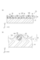
- FIG. 1A is a schematic cross-sectional view of an optical film according to an embodiment of the present disclosure
- FIG. 1B is a schematic cross-sectional view for explaining characteristics of a shape that the optical film of the present disclosure preferably has.
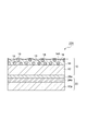
- FIG. 2 is a schematic cross-sectional view of the optical barrier film according to the first embodiment of the present disclosure
- FIG. 3 is a schematic cross-sectional view of an optical barrier film according to a second embodiment of the present disclosure.
- FIG. 4 is a schematic cross-sectional view of an optical barrier film according to a third embodiment of the present disclosure.
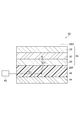
- FIG. 5 is a schematic cross-sectional view of a color conversion film including an optical barrier film according to an embodiment of the present disclosure.
- FIG. 1A is a schematic cross-sectional view of an optical film according to an embodiment of the present disclosure
- FIG. 1B is a schematic cross-sectional view for explaining characteristics of a shape that the optical film of the present disclosure preferably has.
- FIG. 2 is a schematic cross-section
- FIG. 6 is a schematic cross-sectional view of a backlight unit according to an embodiment of the present disclosure.
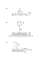
- 7 (a) to 7 (c) are tests for evaluating the scratch resistance of the light guide plate.
- FIG. 7 (a) is a pressure test
- FIG. 7 (b) is a falling ball test
- FIG. 7 (c) is a scratch. It is a schematic sectional drawing for demonstrating each method of a test.
- an optical film according to an embodiment of the present disclosure an optical barrier film including the optical film, and a backlight unit will be described with reference to the drawings.
- the same reference numerals are assigned to the same components unless there is a reason for convenience.
- the thicknesses and ratios of the constituent elements may be exaggerated for easy viewing. Further, the present invention is not limited to the following embodiments without departing from the gist thereof.
- FIG. 1A is a schematic cross-sectional view of an optical film according to an embodiment of the present disclosure.
- the optical film 10 includes a first film substrate 12 and a light diffusion layer 14 formed on the first film substrate 12.
- the light diffusing layer 14 includes a binder resin 16 and light diffusing particles 18, and more than 10% of the number of the light diffusing particles 18 protrudes partly from the vicinity where the light diffusing particles 18 do not exist, thereby diffusing the light.
- An uneven structure is formed on the surface of the layer 14. Further, 90% or more of the number of the light diffusing particles 18 protruding partly is coated with the binder resin 16 on the protruding part.
- 10% or more of the number of the light diffusing particles 18 means that at least 5 of the light diffusing particles 18 are observed by cross-sectional observation using an optical microscope or an electron microscope. Moreover, 90% or more of the number of the light-diffusing particles 18 partially protruding means 90% or more of the five or more.
- FIG. 1B is a schematic cross-sectional view for explaining the characteristics of the shape that the optical film 10 preferably has.
- the optical film 10 is the most vertically (+ Z direction) from the plane determined by the interface between the first film substrate 12 and the light diffusing layer 14.
- the average value of the thickness S of the binder resin covering the high part is preferably 50 nm or more and 1 ⁇ m or less.
- the average value of the thickness S is an average value obtained by measuring the binder resin 16 covering the protruding portions of the light diffusion particles 18 at 20 points by cross-sectional observation using an optical microscope or an electron microscope.
- the average value of the thickness S is less than 50 nm, the covering effect is not sufficiently exhibited, and there is a risk of damaging the light diffusion layer 14 when it comes into contact with other members or the risk of the light diffusion particles 18 falling off. Get higher. If the average value of the thickness S is greater than 1 ⁇ m, the surface irregularities become large, and there is a concern that the optical characteristics such as haze deviate from the optimum values.
- the optical film 10 has an average value of the height H of the protruding portion of the light diffusing particles 18 from the plane 14C determined by the average film thickness T of the light diffusing layer 14 having a concavo-convex structure.
- the average particle diameter R of the particles 18 is preferably 10% or more and less than 50%.
- the average film thickness T of the light diffusion layer 14 having a concavo-convex structure can be obtained by an electronic micrometer or a fully automatic fine shape measuring machine.
- the average value of the height H is an average value obtained by measuring the height H of the protruding portion of the light diffusing particle 18 by 20 cross-sectional observations using an optical microscope or an electron microscope.
- the average particle diameter R of the light diffusing particles 18 in the light diffusing layer 14 is, for example, about 20 light diffusing particles 18 randomly extracted by observing the surface of the optical film 10 with an optical microscope or an electron microscope.
- the height H of the protruding portion of the light diffusion particle 18 is less than 10% of the average particle diameter R, a suitable haze value cannot be obtained, and when it exceeds 50%, sufficient coating with the binder resin is not achieved.
- the light diffusion layer 14 comes into contact with other members, the risk of damaging them or the risk of the light diffusion particles 18 falling off increases.
- the average particle diameter R of the light diffusion particles 18 in the light diffusion layer 14 is preferably 0.5 ⁇ m or more and 10 ⁇ m or less. If the average particle diameter R is less than 0.5 ⁇ m, a suitable haze value cannot be obtained, and if it exceeds 10 ⁇ m, there is a concern that other members that come into contact may be damaged.
- the optical film 10 preferably has a surface resistivity of the light diffusion layer 14 of 1.0 ⁇ 10 13 ⁇ / ⁇ or less.
- the light diffusing layer 14 is preferably provided with antistatic performance, so that the adhesion or mixing of dust or the like to the light diffusing layer 14 tends to decrease. For this reason, in the manufacturing process of a backlight unit, etc., there is a tendency that damage to the light diffusion layer 14 or other members due to dust is reduced.
- FIG. 2 is a schematic cross-sectional view of the optical barrier film according to the first embodiment of the present disclosure.
- the optical barrier film 20A includes the barrier composite layer 22 including the second film base 12a and the barrier layer 24a, and the optical film 10 of FIG.
- the barrier composite layer 22 is formed on the optical film 10 via the adhesive layer 26a so that the first film substrate 12 and the barrier layer 24a face each other.
- the optical barrier film 20A realizes an optical barrier film that has excellent water vapor barrier properties and oxygen barrier properties and further reduces damage to the barrier layers and the like. it can.
- the material of the second film substrate 12a may be the same as that of the first film substrate 12.
- the thickness of the second film substrate 12a is preferably 5 ⁇ m or more and 50 ⁇ m or less, for example. When the thickness of the second film substrate 12a is 5 ⁇ m or more, the strength of the second film substrate 12a is improved. For example, in the backlight unit manufacturing process, the second film substrate 12a can be easily handled. Tend to be. On the other hand, when the thickness of the second film substrate 12a is 50 ⁇ m or less, it is possible to suppress a decrease in barrier properties due to intrusion of water vapor or oxygen from the substrate end surface.
- the barrier layer 24a is a layer that can block gas intrusion.
- the barrier layer 24a preferably includes an inorganic thin film layer.
- the inorganic thin film layer preferably contains an inorganic oxide such as a metal oxide.
- the metal include aluminum, copper, and silver.
- the metal oxide can be, for example, at least one metal oxide selected from the group consisting of yttrium tantalum oxide, aluminum oxide, silicon oxide, and magnesium oxide, and is inexpensive. From the viewpoint of excellent barrier performance for blocking intrusion of water vapor or the like, silicon oxide is preferable.
- the silicon oxide is represented by SiOx, and x in the formula is preferably 1.5 or more and 2.0 or less. When x is 1.5 or more, more preferably 1.7 or more, the transparency tends to be improved.
- the inorganic thin film layer is preferably formed by, for example, an evaporation method or a sputtering method, and is an inorganic evaporation thin film layer formed by an evaporation method.
- the thickness of the inorganic thin film layer is preferably 10 to 300 nm, and more preferably 20 to 100 nm.
- the thickness of the inorganic thin film layer is 10 nm or more, a uniform film tends to be obtained and gas barrier properties tend to be easily obtained.
- the thickness of the inorganic thin film layer is 300 nm or less, the inorganic thin film layer can be kept flexible, and cracks and the like tend not to occur due to external forces such as bending and pulling after film formation.
- the barrier layer 24a may include a gas barrier coating layer.
- the gas barrier coating layer is preferably formed from a composition containing at least one selected from the group consisting of a metal alkoxide represented by the following formula (1) and a hydrolyzate thereof.
- R 1 and R 2 are each independently a monovalent organic group having 1 to 8 carbon atoms, preferably an alkyl group such as a methyl group or an ethyl group.
- M represents an n-valent metal atom such as Si, Ti, Al, or Zr.
- m is an integer of 1 to n.
- the metal alkoxide include tetraethoxysilane [Si (OC 2 H 5 ) 4 ], triisopropoxyaluminum [Al (O-iso-C 3 H 7 ) 3 ] and the like.
- the metal alkoxide is preferably tetraethoxysilane or triisopropoxyaluminum because it is relatively stable in an aqueous solvent after hydrolysis.
- Examples of the hydrolyzate of the metal alkoxide include silicic acid (Si (OH) 4 ) that is a hydrolyzate of tetraethoxysilane and aluminum hydroxide (Al (OH) 3 that is a hydrolyzate of tripropoxyaluminum. ) And the like. These can be used in combination of not only one type but also a plurality of types.
- the above composition may further contain a hydroxyl group-containing polymer compound.
- the hydroxyl group-containing polymer compound include water-soluble polymers such as polyvinyl alcohol, polyvinyl pyrrolidone and starch.
- the hydroxyl group-containing polymer compound is preferably polyvinyl alcohol from the viewpoint of barrier properties. These can be used in combination of not only one type but also a plurality of types.
- the content of the hydroxyl group-containing polymer compound in the composition is, for example, 10 to 90% by mass.
- the thickness of the gas barrier coating layer is preferably 50 to 1000 nm, and preferably 100 to 500 nm. When the thickness of the gas barrier coating layer is 50 nm or more, a sufficient gas barrier property tends to be obtained, and when it is 1000 nm or less, a sufficient flexibility tends to be maintained.
- the barrier layer 24a includes both the inorganic thin film layer and the gas barrier coating layer
- the inorganic thin film layer is formed on the surface of the first film substrate 12
- the gas barrier coating layer is formed on the surface of the inorganic thin film layer. It may be.
- the adhesive layer 26a is formed from an adhesive or a pressure-sensitive adhesive.
- the adhesive include acrylic adhesives, epoxy adhesives, urethane adhesives, and the like.
- the adhesive preferably includes an epoxy resin. When the adhesive contains an epoxy resin, the adhesion between the optical film 10 and the barrier composite layer 22 can be improved.
- the pressure-sensitive adhesive include acrylic pressure-sensitive adhesives, polyvinyl ether-based pressure-sensitive adhesives, urethane-based pressure-sensitive adhesives, silicone-based pressure-sensitive adhesives, and starch paste-based adhesives.
- the thickness of the adhesive layer 26a is preferably 0.5 to 50 ⁇ m, more preferably 1 to 20 ⁇ m, and even more preferably 2 to 6 ⁇ m. When the thickness of the adhesive layer 26a is 0.5 ⁇ m or more, the adhesion between the optical film 10 and the barrier composite layer 22 is easily obtained, and when the thickness is 50 ⁇ m or less, more excellent gas barrier properties. Tends to be easily obtained.
- the optical barrier film 20A according to the first embodiment forms the barrier composite layer 22 by forming the barrier layer 24a on the second film substrate 12a separately from the optical film 10, and then the optical film 10 and the barrier. It can be obtained by laminating the composite layer 22 and performing aging as necessary.
- the manufacturing method of the optical barrier film 20A according to the first embodiment is not limited to the above.
- FIG. 3 is a schematic cross-sectional view of an optical barrier film according to a second embodiment of the present disclosure.
- the optical barrier film 20 ⁇ / b> B includes the barrier composite layer 22 a including the second film substrate 12 a and the barrier layer 24 a, and the optical film 10.
- the barrier composite layer 22a is formed on the optical film 10 via the adhesive layer 26a so that the first film substrate 12 and the second film substrate 12a face each other.
- FIG. 4 is a schematic cross-sectional view of an optical barrier film according to a third embodiment of the present disclosure.
- the optical barrier film 20C includes a barrier composite layer 22a including the second film base 12a and the barrier layer 24a, a barrier composite layer 22b including the third film base 12b and the barrier layer 24b, and the optical film 10.
- the barrier composite layer 22a is formed on the optical film 10 via the adhesive layer 26a so that the first film substrate 12 and the second film substrate 12a face each other.
- the barrier composite layer 22b is formed on the barrier composite layer 22a with an adhesive layer 26b so that the barrier layer 24a and the barrier layer 24b face each other.
- FIG. 5 is a schematic cross-sectional view of a color conversion film including an optical barrier film according to an embodiment of the present disclosure.
- the color conversion film 30 is a film that can convert some wavelengths of light from the light source of the backlight unit for liquid crystal display.
- the color conversion film 30 includes a color conversion layer 32 and an optical barrier film 20 arranged so as to sandwich the color conversion layer 32.
- the optical barrier film 20 may be any of the optical barrier films 20A, 20B, and 20C described above, and the configurations of the two optical barrier films 20 may be the same as or different from each other.
- the optical barrier film 20 is disposed on the color conversion layer 32 so that the light diffusion layer 14 faces the side opposite to the color conversion layer 32. Therefore, the color conversion film 30 has the uneven surfaces 20F and 20G derived from the uneven surface 14A of the light diffusion layer 14.
- the color conversion film 30 has uneven surfaces 20F and 20G on the surface, so that when other members are stacked on the uneven surfaces 20F and 20G of the color conversion film 30, blocking with the other members can be suppressed. it can. Moreover, even if the color conversion film 30 is overlapped with, for example, the light guide plate constituting the backlight unit, it is possible to suppress the light conversion plate from being damaged by the light diffusion particles protruding. In addition, since the barrier layer itself is also prevented from being damaged, the intrusion of air and water vapor into the color conversion layer 32 is appropriately reduced, and the color conversion performance in the color conversion film 30 is maintained for a long period of time.
- the color conversion film according to the present disclosure is not limited to the above embodiment.
- the color conversion film 30 having the configuration in which the color conversion layer 32 is sandwiched between two protective films made of the optical barrier film according to the present disclosure is illustrated.
- One may be an optical barrier film according to the present disclosure, and the other may be a protective film having another configuration.
- the color conversion layer 32 includes a resin and a phosphor, and the thickness of the color conversion layer 32 is several tens to several hundreds ⁇ m.
- the resin for example, a photocurable resin or a thermosetting resin can be used.
- the color conversion layer 32 preferably includes two types of phosphors made of luminescent nanocrystals (quantum dots).
- the color conversion layer 32 may be formed by laminating two or more phosphor layers including one type of phosphor and another type of phosphor. Two types of phosphors having the same excitation wavelength are selected. The excitation wavelength is selected based on the wavelength of light emitted from the light source of the backlight unit. The fluorescent colors of the two types of phosphors are different from each other.
- the two types of fluorescent colors are red and green.
- the wavelength of each fluorescence and the wavelength of light emitted from the light source are selected based on the spectral characteristics of the color filter.
- the peak wavelength of fluorescence is, for example, 610 nm for red and 550 nm for green.
- FIG. 6 is a schematic cross-sectional view of a backlight unit according to an embodiment of the present disclosure.
- the backlight unit 40 includes a light source 42, a light guide plate 46, and a color conversion film 30 disposed on the light guide plate 46.
- the color conversion film 30 is disposed so that the uneven surface 20 ⁇ / b> F (that is, the uneven surface 14 ⁇ / b> A of the light diffusion layer 14) is in contact with the light guide plate 46.
- the light guide plate 46 and the reflection plate 44 are arranged in this order on the uneven surface 20F of the color conversion film 30, and the light source 42 is located on the side of the light guide plate 46 (the surface of the light guide plate 46).
- the light guide plate 46 and the reflection plate 44 are arranged in this order on the uneven surface 20F of the color conversion film 30, and the light source 42 is located on the side of the light guide plate 46 (the surface of the light guide plate 46).
- the backlight unit 40 includes the color conversion film 30 having sufficiently small in-plane performance variations, whereby variations in performance (color development, luminance, etc.) of the backlight unit 40 can be sufficiently reduced.
- the backlight unit 40 can suppress the light guide plate 46 in contact with the color conversion film 30 from being damaged. Further, since the barrier layer itself is also prevented from being damaged, the intrusion of air and water vapor into the color conversion layer is appropriately reduced, and good white light can be obtained from the backlight unit over a long period of time. it can.
- the light guide plate 46 and the reflection plate 44 efficiently reflect and guide the light emitted from the light source 42, and a known material is used.
- a known material is used as the light guide plate 46.
- acrylic, polycarbonate, cycloolefin film, or the like is used.
- the material used for the light guide plate 46 often does not have a large hardness and tends to be easily damaged by contact with other members.
- polycarbonate is generally used because of its high transparency and ease of processing, but it has a low surface hardness and is easily damaged.
- the light source 42 includes a plurality of blue light emitting diode elements.
- the light emitting diode element may be a violet light emitting diode or a light emitting diode having a lower wavelength.
- the light emitted from the light source 42 enters the light guide plate 46 (D1 direction), and then enters the color conversion layer 32 (D2 direction) with reflection and refraction.
- the light that has passed through the color conversion layer 32 becomes white light by mixing the yellow light generated in the color conversion layer 32 with the light before passing through the color conversion layer 32.
- optical film of the present disclosure will be described more specifically based on examples and comparative examples, the scope of the present invention is not limited to the following examples.
- a light diffusion layer composition obtained by mixing the compositions shown in Table 1 was applied, and a coating film was formed by a wire bar coater. Subsequently, this coating film was dried by heating at 80 ° C. for 30 seconds. The dried coating film was aged at 60 ° C. for 2 days to produce optical films of Examples 1 to 13 and Comparative Examples 1 and 2, respectively.
- a coating film of the light diffusion layer composition use different wire bars with different counts and change the coating amount by adjusting the viscosity. Formed respectively.
- the measurement was performed by observing the cross section of the light diffusion layer with an electron microscope at any part of the film. That is, the number% of the light diffusing particles having protruding portions is counted for each of the 50 light diffusing particles extracted at random and those that do not protrude, and the optical films of Examples and Comparative Examples are both. It was confirmed that 10% or more of the number protruded partly from the vicinity of the periphery where no light diffusing particles were present. Further, the ratio of the number of the light diffusing particles protruding partly covered with the binder resin is 100% for the optical films of the examples, and 0% for the optical films of the comparative examples. Met.
- the average value of the thickness of the binder resin that covers the highest portion of the protruding portion of the light diffusing particles was measured on 20 light diffusing particles that were randomly extracted and covered with the protruding binder resin.
- the average value of the height of the protruding portion of the light diffusing particles from the plane determined by the average film thickness of the light diffusing layer and the average particle diameter of the light diffusing particles in the light diffusing layer are both randomly extracted and protruding 20 Measurements were made on individual light diffusing particles.
- the surface resistivity was measured according to JIS-K6911 using a high resistivity meter (trade name: Hirestar UP MCP-HT450, manufactured by Dia Instruments) (applied voltage: 500 V, time: 10 seconds, probe) : URS condition, 23 ° C. and 55% RH environment).
- a high resistivity meter (trade name: Hirestar UP MCP-HT450, manufactured by Dia Instruments) (applied voltage: 500 V, time: 10 seconds, probe) : URS condition, 23 ° C. and 55% RH environment).
- Table 2 shows the following values. -Value 1: Ratio of light diffusing particles partially protruding (unit:%) Value 2: The thickness of the binder resin that covers the highest part in the vertical direction from the plane determined by the interface between the first film substrate and the light diffusion layer among the thickness of the binder resin that covers the protruding part of the light diffusion particle.
- FIG. 7 (a) to 7 (c) are tests for evaluating the scratch resistance of the light guide plate.
- FIG. 7 (a) is a pressure test
- FIG. 7 (b) is a falling ball test
- FIG. 7 (c) is a scratch.
- the optical film F is an evaluation target.
- a polycarbonate film 50 (thickness: 30 ⁇ m) imitating the light guide plate of the backlight unit was disposed below the optical film F.
- An optical film F to be evaluated (4 cm long ⁇ 4 cm wide) was prepared.
- An optical film F was disposed on the surface of the polycarbonate film 50.
- the direction of the optical film F was such that the light diffusion layer of the optical film F faces the polycarbonate film 50.
- a silicone rubber sheet 60 was placed on the surface of the optical film F.
- a load was applied to the optical film F with the jig J (bottom area: 1 cm 2 ), and the plate was left at room temperature for 30 seconds under a load of 25 kgf / cm 2 . Then, the surface of the light-diffusion layer and the polycarbonate film was observed visually and with an optical microscope, and the presence or absence of scratches and the state were evaluated.
- Table 3 shows the evaluation results of the light-guiding plate scratchability by the above (a) pressure test (b) falling ball test (c) scratch test.
- the evaluation criteria were as follows. A ... No scratch (OK) B ... with very thin scratches (OK) C ... Slight scratch (OK) D ... Dark scratches (NG) ⁇ Comprehensive evaluation> ⁇ All A (OK) ⁇ All A or B (OK) ⁇ ... C (OK) ⁇ ... D (NG)
- the optical film of Example 1 had the best results in both the light guide plate scratchability evaluation and the peeling evaluation, and the haze value also coincided with the target value.
- the average particle diameter of the light diffusing particles was as large as 10 ⁇ m, and thus very thin scratches were observed in the light guide plate scratchability evaluation.
- the optical film of Example 2 since the average value of the thickness of the binder resin covering the highest portion of the protruding portion of the light diffusing particles was as thick as 1.5 ⁇ m, the haze became large and approached the allowable limit.
- the optical film of Example 3 has a very thin scratch in the light guide plate scratchability evaluation because the average value of the thickness of the binder resin covering the highest portion of the protruding portion of the light diffusing particles is as thin as 30 nm. It was seen.
- an optical film in which a risk of damaging the light diffusing layer when contacting with other members and a risk of light diffusing particles falling off, and an optical barrier film and a backlight including the optical film are reduced. Units are provided.
- SYMBOLS 10 Optical film, 12 ... 1st film base material, 12a ... 2nd film base material, 12b ... 3rd film base material, 14 ... Light diffusion layer, 14A ... Uneven surface, 14C ... By the average film thickness of a light diffusion layer Planar surface, 16 ... Binder resin, 18 ... Light diffusion particles, 20, 20A, 20B, 20C ... Optical barrier film, 20F, 20G ... Rough surface, 22, 22a, 22b ... Barrier composite layer, 24a, 24b ... Barrier layer, 26a, 26b ... adhesive layer, 30 ... color conversion film, 32 ... color conversion layer, 40 ... backlight unit, 42 ... light source, 44 ... reflector, 46 ... light guide plate
Landscapes
- Physics & Mathematics (AREA)
- General Physics & Mathematics (AREA)
- Optics & Photonics (AREA)
- Chemical & Material Sciences (AREA)
- Dispersion Chemistry (AREA)
- Engineering & Computer Science (AREA)
- General Engineering & Computer Science (AREA)
- Optical Elements Other Than Lenses (AREA)
- Liquid Crystal (AREA)
- Laminated Bodies (AREA)
- Planar Illumination Modules (AREA)
Abstract
Priority Applications (4)
| Application Number | Priority Date | Filing Date | Title |
|---|---|---|---|
| KR1020207028045A KR102783625B1 (ko) | 2018-03-07 | 2019-03-07 | 광학 필름, 광학 배리어 필름, 및 백라이트 유닛 |
| CN201980016457.2A CN111954831B (zh) | 2018-03-07 | 2019-03-07 | 光学膜、光学阻隔膜以及背光单元 |
| JP2020505117A JP7331830B2 (ja) | 2018-03-07 | 2019-03-07 | 光学フィルム、光学バリアフィルム、及びバックライトユニット |
| US17/013,053 US11650358B2 (en) | 2018-03-07 | 2020-09-04 | Optical film, optical barrier film, and backlight unit |
Applications Claiming Priority (2)
| Application Number | Priority Date | Filing Date | Title |
|---|---|---|---|
| JP2018040729 | 2018-03-07 | ||
| JP2018-040729 | 2018-03-07 |
Related Child Applications (1)
| Application Number | Title | Priority Date | Filing Date |
|---|---|---|---|
| US17/013,053 Continuation US11650358B2 (en) | 2018-03-07 | 2020-09-04 | Optical film, optical barrier film, and backlight unit |
Publications (1)
| Publication Number | Publication Date |
|---|---|
| WO2019172384A1 true WO2019172384A1 (fr) | 2019-09-12 |
Family
ID=67845645
Family Applications (1)
| Application Number | Title | Priority Date | Filing Date |
|---|---|---|---|
| PCT/JP2019/009150 Ceased WO2019172384A1 (fr) | 2018-03-07 | 2019-03-07 | Film optique, film de barrière optique et unité de rétroéclairage |
Country Status (5)
| Country | Link |
|---|---|
| US (1) | US11650358B2 (fr) |
| JP (1) | JP7331830B2 (fr) |
| KR (1) | KR102783625B1 (fr) |
| CN (1) | CN111954831B (fr) |
| WO (1) | WO2019172384A1 (fr) |
Cited By (1)
| Publication number | Priority date | Publication date | Assignee | Title |
|---|---|---|---|---|
| WO2023058742A1 (fr) * | 2021-10-08 | 2023-04-13 | 日本電気硝子株式会社 | Article transparent |
Families Citing this family (1)
| Publication number | Priority date | Publication date | Assignee | Title |
|---|---|---|---|---|
| JP2022169991A (ja) * | 2021-04-28 | 2022-11-10 | 株式会社きもと | 成型拡散積層フィルム |
Citations (5)
| Publication number | Priority date | Publication date | Assignee | Title |
|---|---|---|---|---|
| JP2001350005A (ja) * | 2000-06-09 | 2001-12-21 | Tomoegawa Paper Co Ltd | 光学シートおよびその製造方法 |
| JP2002099220A (ja) * | 2000-09-26 | 2002-04-05 | Keiwa Inc | 光拡散シート及びこれを用いたバックライトユニット |
| JP2014130234A (ja) * | 2012-12-28 | 2014-07-10 | Keiwa Inc | 光学シート及びバックライトユニット |
| WO2016076322A1 (fr) * | 2014-11-14 | 2016-05-19 | 凸版印刷株式会社 | Film optique, film barrière optique utilisant celui-ci, film de conversion de couleur et unité de rétro-éclairage |
| JP2017102389A (ja) * | 2015-12-04 | 2017-06-08 | 凸版印刷株式会社 | 光学フィルム、並びに、それを用いた光学バリアフィルム、色変換フィルム及びバックライトユニット |
Family Cites Families (17)
| Publication number | Priority date | Publication date | Assignee | Title |
|---|---|---|---|---|
| JP3790571B2 (ja) | 1995-11-06 | 2006-06-28 | 株式会社きもと | 光拡散性シートおよびそれを用いた液晶ディスプレイ用バックライトユニット |
| US7072115B2 (en) * | 2002-03-26 | 2006-07-04 | Keiwa Inc. | Light diffusion sheet and backlight unit using the same |
| JP2005165252A (ja) * | 2003-11-14 | 2005-06-23 | Sony Corp | 光機能性拡散板、反射型スクリーン及びその製造方法 |
| KR100716144B1 (ko) * | 2005-10-21 | 2007-05-10 | 도레이새한 주식회사 | 박막트랜지스터 액정디스플레이용 확산시트 |
| JP2008209919A (ja) * | 2007-02-02 | 2008-09-11 | Toray Ind Inc | 光学用シートおよび光学用シートの製造方法 |
| JP2009237148A (ja) * | 2008-03-26 | 2009-10-15 | Asahi Kasei Corp | 光拡散シート及びバックライトユニット |
| JP2010191412A (ja) * | 2009-01-21 | 2010-09-02 | Toppan Printing Co Ltd | 防眩フィルム |
| EP2638321B1 (fr) * | 2010-11-10 | 2019-05-08 | Nanosys, Inc. | Films constitués de points quantiques, dispositifs d'éclairage et procédés d'éclairage |
| US20120213967A1 (en) * | 2011-02-23 | 2012-08-23 | Hosoda Hidemasa | Optical laminate film and display device |
| JP5915524B2 (ja) * | 2011-03-18 | 2016-05-11 | 東レ株式会社 | 積層フィルムおよびその製造方法 |
| KR20130035118A (ko) * | 2011-09-29 | 2013-04-08 | 엘지디스플레이 주식회사 | 휘도를 향상시키는 확산시트 및 이를 구비한 액정표시소자 |
| KR101251815B1 (ko) * | 2011-11-07 | 2013-04-09 | 엘지이노텍 주식회사 | 광학 시트 및 이를 포함하는 표시장치 |
| WO2013096324A1 (fr) * | 2011-12-21 | 2013-06-27 | 3M Innovative Properties Company | Empilement de films optiques |
| KR101908656B1 (ko) * | 2012-04-09 | 2018-10-16 | 엘지이노텍 주식회사 | 발광 소자 패키지 |
| EP3208520B1 (fr) * | 2014-10-16 | 2023-05-03 | Toppan Printing Co., Ltd. | Film de protection de points quantiques, film de points quantiques l'utilisant, et unité de rétroéclairage |
| WO2017048957A1 (fr) * | 2015-09-15 | 2017-03-23 | 3M Innovative Properties Company | Revêtements mats à faible brillance et procédés de fabrication |
| US10386567B2 (en) * | 2016-05-16 | 2019-08-20 | Keiwa Inc. | Optical sheet for liquid crystal display device, backlight unit for liquid crystal display device and production method of optical sheet for liquid crystal display device |
-
2019
- 2019-03-07 WO PCT/JP2019/009150 patent/WO2019172384A1/fr not_active Ceased
- 2019-03-07 CN CN201980016457.2A patent/CN111954831B/zh active Active
- 2019-03-07 KR KR1020207028045A patent/KR102783625B1/ko active Active
- 2019-03-07 JP JP2020505117A patent/JP7331830B2/ja active Active
-
2020
- 2020-09-04 US US17/013,053 patent/US11650358B2/en active Active
Patent Citations (5)
| Publication number | Priority date | Publication date | Assignee | Title |
|---|---|---|---|---|
| JP2001350005A (ja) * | 2000-06-09 | 2001-12-21 | Tomoegawa Paper Co Ltd | 光学シートおよびその製造方法 |
| JP2002099220A (ja) * | 2000-09-26 | 2002-04-05 | Keiwa Inc | 光拡散シート及びこれを用いたバックライトユニット |
| JP2014130234A (ja) * | 2012-12-28 | 2014-07-10 | Keiwa Inc | 光学シート及びバックライトユニット |
| WO2016076322A1 (fr) * | 2014-11-14 | 2016-05-19 | 凸版印刷株式会社 | Film optique, film barrière optique utilisant celui-ci, film de conversion de couleur et unité de rétro-éclairage |
| JP2017102389A (ja) * | 2015-12-04 | 2017-06-08 | 凸版印刷株式会社 | 光学フィルム、並びに、それを用いた光学バリアフィルム、色変換フィルム及びバックライトユニット |
Cited By (1)
| Publication number | Priority date | Publication date | Assignee | Title |
|---|---|---|---|---|
| WO2023058742A1 (fr) * | 2021-10-08 | 2023-04-13 | 日本電気硝子株式会社 | Article transparent |
Also Published As
| Publication number | Publication date |
|---|---|
| JP7331830B2 (ja) | 2023-08-23 |
| CN111954831B (zh) | 2024-02-02 |
| KR20200128704A (ko) | 2020-11-16 |
| US20200400864A1 (en) | 2020-12-24 |
| JPWO2019172384A1 (ja) | 2021-03-25 |
| CN111954831A (zh) | 2020-11-17 |
| US11650358B2 (en) | 2023-05-16 |
| KR102783625B1 (ko) | 2025-03-18 |
Similar Documents
| Publication | Publication Date | Title |
|---|---|---|
| US20250189696A1 (en) | Antireflective member, and polarizing plate, image display device and antireflective article each equipped with same | |
| EP3064829B1 (fr) | Feuille de conversion de longueur d'onde et unité de rétroéclairage | |
| US10557970B2 (en) | Quantum dot protective film, and wavelength conversion sheet and backlight unit obtained by using the same | |
| US10072184B2 (en) | Pressure-sensitive adhesive sheet having a transparent pressure-sensitive adhesive layer | |
| KR102536613B1 (ko) | 배리어 필름, 파장 변환 시트, 백 라이트, 및 표시 장치 | |
| US11397287B2 (en) | Optical film, and optical barrier film, color conversion film and backlight unit using the optical film | |
| KR20220007614A (ko) | 배리어 필름, 그것을 이용한 파장 변환 시트 및 그것을 이용한 표시 장치 | |
| KR102205622B1 (ko) | 광학 적층체 및 면광원 장치 | |
| WO2023058626A1 (fr) | Film d'utilisation de feuille de conversion de longueur d'onde, feuille de conversion de longueur d'onde, rétroéclairage et dispositif d'affichage | |
| US11650358B2 (en) | Optical film, optical barrier film, and backlight unit | |
| JP6717295B2 (ja) | 色変換フィルム | |
| JP2019008906A (ja) | 波長変換フィルム及びバックライトユニット | |
| JP2020042137A (ja) | 光学フィルム、光学バリアフィルム、及び波長変換フィルム | |
| JP6772520B2 (ja) | 波長変換シート | |
| KR20220136902A (ko) | 하드 코트 필름, 광학 부재, 및 화상 표시 장치 | |
| JP7467881B2 (ja) | 量子ドット保護フィルム | |
| WO2024225410A1 (fr) | Feuille de conversion de longueur d'onde, rétroéclairage et dispositif d'affichage à cristaux liquides | |
| JP2023047016A (ja) | 波長変換シート用フィルム、波長変換シート、バックライト、及び表示装置 | |
| JP2020144159A (ja) | 剥離フィルム付蛍光体保護フィルムおよび波長変換シート | |
| KR20070011702A (ko) | 액정디스플레이 백라이트 유니트용 광확산 시트 |
Legal Events
| Date | Code | Title | Description |
|---|---|---|---|
| 121 | Ep: the epo has been informed by wipo that ep was designated in this application |
Ref document number: 19764810 Country of ref document: EP Kind code of ref document: A1 |
|
| ENP | Entry into the national phase |
Ref document number: 2020505117 Country of ref document: JP Kind code of ref document: A |
|
| NENP | Non-entry into the national phase |
Ref country code: DE |
|
| ENP | Entry into the national phase |
Ref document number: 20207028045 Country of ref document: KR Kind code of ref document: A |
|
| 122 | Ep: pct application non-entry in european phase |
Ref document number: 19764810 Country of ref document: EP Kind code of ref document: A1 |