WO2019176152A1 - 磁性配線回路基板およびその製造方法 - Google Patents
磁性配線回路基板およびその製造方法 Download PDFInfo
- Publication number
- WO2019176152A1 WO2019176152A1 PCT/JP2018/039082 JP2018039082W WO2019176152A1 WO 2019176152 A1 WO2019176152 A1 WO 2019176152A1 JP 2018039082 W JP2018039082 W JP 2018039082W WO 2019176152 A1 WO2019176152 A1 WO 2019176152A1
- Authority
- WO
- WIPO (PCT)
- Prior art keywords
- wiring
- magnetic
- thickness direction
- insulating layer
- thickness
- Prior art date
- Legal status (The legal status is an assumption and is not a legal conclusion. Google has not performed a legal analysis and makes no representation as to the accuracy of the status listed.)
- Ceased
Links
Images


Classifications
-
- H—ELECTRICITY
- H01—ELECTRIC ELEMENTS
- H01F—MAGNETS; INDUCTANCES; TRANSFORMERS; SELECTION OF MATERIALS FOR THEIR MAGNETIC PROPERTIES
- H01F17/00—Fixed inductances of the signal type
- H01F17/0006—Printed inductances
-
- H—ELECTRICITY
- H01—ELECTRIC ELEMENTS
- H01F—MAGNETS; INDUCTANCES; TRANSFORMERS; SELECTION OF MATERIALS FOR THEIR MAGNETIC PROPERTIES
- H01F41/00—Apparatus or processes specially adapted for manufacturing or assembling magnets, inductances or transformers; Apparatus or processes specially adapted for manufacturing materials characterised by their magnetic properties
- H01F41/02—Apparatus or processes specially adapted for manufacturing or assembling magnets, inductances or transformers; Apparatus or processes specially adapted for manufacturing materials characterised by their magnetic properties for manufacturing cores, coils, or magnets
- H01F41/04—Apparatus or processes specially adapted for manufacturing or assembling magnets, inductances or transformers; Apparatus or processes specially adapted for manufacturing materials characterised by their magnetic properties for manufacturing cores, coils, or magnets for manufacturing coils
- H01F41/041—Printed circuit coils
- H01F41/046—Printed circuit coils structurally combined with ferromagnetic material
-
- H—ELECTRICITY
- H01—ELECTRIC ELEMENTS
- H01F—MAGNETS; INDUCTANCES; TRANSFORMERS; SELECTION OF MATERIALS FOR THEIR MAGNETIC PROPERTIES
- H01F17/00—Fixed inductances of the signal type
- H01F17/04—Fixed inductances of the signal type with magnetic core
-
- H—ELECTRICITY
- H01—ELECTRIC ELEMENTS
- H01F—MAGNETS; INDUCTANCES; TRANSFORMERS; SELECTION OF MATERIALS FOR THEIR MAGNETIC PROPERTIES
- H01F27/00—Details of transformers or inductances, in general
- H01F27/34—Special means for preventing or reducing unwanted electric or magnetic effects, e.g. no-load losses, reactive currents, harmonics, oscillations, leakage fields
- H01F27/36—Electric or magnetic shields or screens
- H01F27/366—Electric or magnetic shields or screens made of ferromagnetic material
-
- H—ELECTRICITY
- H01—ELECTRIC ELEMENTS
- H01F—MAGNETS; INDUCTANCES; TRANSFORMERS; SELECTION OF MATERIALS FOR THEIR MAGNETIC PROPERTIES
- H01F41/00—Apparatus or processes specially adapted for manufacturing or assembling magnets, inductances or transformers; Apparatus or processes specially adapted for manufacturing materials characterised by their magnetic properties
- H01F41/02—Apparatus or processes specially adapted for manufacturing or assembling magnets, inductances or transformers; Apparatus or processes specially adapted for manufacturing materials characterised by their magnetic properties for manufacturing cores, coils, or magnets
- H01F41/04—Apparatus or processes specially adapted for manufacturing or assembling magnets, inductances or transformers; Apparatus or processes specially adapted for manufacturing materials characterised by their magnetic properties for manufacturing cores, coils, or magnets for manufacturing coils
-
- H—ELECTRICITY
- H01—ELECTRIC ELEMENTS
- H01F—MAGNETS; INDUCTANCES; TRANSFORMERS; SELECTION OF MATERIALS FOR THEIR MAGNETIC PROPERTIES
- H01F41/00—Apparatus or processes specially adapted for manufacturing or assembling magnets, inductances or transformers; Apparatus or processes specially adapted for manufacturing materials characterised by their magnetic properties
- H01F41/02—Apparatus or processes specially adapted for manufacturing or assembling magnets, inductances or transformers; Apparatus or processes specially adapted for manufacturing materials characterised by their magnetic properties for manufacturing cores, coils, or magnets
- H01F41/04—Apparatus or processes specially adapted for manufacturing or assembling magnets, inductances or transformers; Apparatus or processes specially adapted for manufacturing materials characterised by their magnetic properties for manufacturing cores, coils, or magnets for manufacturing coils
- H01F41/041—Printed circuit coils
-
- H—ELECTRICITY
- H01—ELECTRIC ELEMENTS
- H01F—MAGNETS; INDUCTANCES; TRANSFORMERS; SELECTION OF MATERIALS FOR THEIR MAGNETIC PROPERTIES
- H01F5/00—Coils
- H01F5/003—Printed circuit coils
-
- H—ELECTRICITY
- H02—GENERATION; CONVERSION OR DISTRIBUTION OF ELECTRIC POWER
- H02J—ELECTRIC POWER NETWORKS; CIRCUIT ARRANGEMENTS OR SYSTEMS FOR SUPPLYING OR DISTRIBUTING ELECTRIC POWER; SYSTEMS FOR STORING ELECTRIC ENERGY
- H02J50/00—Circuit arrangements or systems for wireless supply or distribution of electric power
- H02J50/10—Circuit arrangements or systems for wireless supply or distribution of electric power using inductive coupling
-
- H—ELECTRICITY
- H05—ELECTRIC TECHNIQUES NOT OTHERWISE PROVIDED FOR
- H05K—PRINTED CIRCUITS; CASINGS OR CONSTRUCTIONAL DETAILS OF ELECTRIC APPARATUS; MANUFACTURE OF ASSEMBLAGES OF ELECTRICAL COMPONENTS
- H05K1/00—Printed circuits
- H05K1/16—Printed circuits incorporating printed electric components, e.g. printed resistors, capacitors or inductors
- H05K1/165—Printed circuits incorporating printed electric components, e.g. printed resistors, capacitors or inductors incorporating printed inductors
-
- H—ELECTRICITY
- H01—ELECTRIC ELEMENTS
- H01F—MAGNETS; INDUCTANCES; TRANSFORMERS; SELECTION OF MATERIALS FOR THEIR MAGNETIC PROPERTIES
- H01F17/00—Fixed inductances of the signal type
- H01F17/0006—Printed inductances
- H01F2017/0066—Printed inductances with a magnetic layer
-
- H—ELECTRICITY
- H01—ELECTRIC ELEMENTS
- H01F—MAGNETS; INDUCTANCES; TRANSFORMERS; SELECTION OF MATERIALS FOR THEIR MAGNETIC PROPERTIES
- H01F17/00—Fixed inductances of the signal type
- H01F17/04—Fixed inductances of the signal type with magnetic core
- H01F2017/048—Fixed inductances of the signal type with magnetic core with encapsulating core, e.g. made of resin and magnetic powder
-
- H—ELECTRICITY
- H01—ELECTRIC ELEMENTS
- H01F—MAGNETS; INDUCTANCES; TRANSFORMERS; SELECTION OF MATERIALS FOR THEIR MAGNETIC PROPERTIES
- H01F38/00—Adaptations of transformers or inductances for specific applications or functions
- H01F38/14—Inductive couplings
-
- H—ELECTRICITY
- H05—ELECTRIC TECHNIQUES NOT OTHERWISE PROVIDED FOR
- H05K—PRINTED CIRCUITS; CASINGS OR CONSTRUCTIONAL DETAILS OF ELECTRIC APPARATUS; MANUFACTURE OF ASSEMBLAGES OF ELECTRICAL COMPONENTS
- H05K2201/00—Indexing scheme relating to printed circuits covered by H05K1/00
- H05K2201/08—Magnetic details
- H05K2201/083—Magnetic materials
- H05K2201/086—Magnetic materials for inductive purposes, e.g. printed inductor with ferrite core
-
- H—ELECTRICITY
- H05—ELECTRIC TECHNIQUES NOT OTHERWISE PROVIDED FOR
- H05K—PRINTED CIRCUITS; CASINGS OR CONSTRUCTIONAL DETAILS OF ELECTRIC APPARATUS; MANUFACTURE OF ASSEMBLAGES OF ELECTRICAL COMPONENTS
- H05K2201/00—Indexing scheme relating to printed circuits covered by H05K1/00
- H05K2201/09—Shape and layout
- H05K2201/09209—Shape and layout details of conductors
- H05K2201/09654—Shape and layout details of conductors covering at least two types of conductors provided for in H05K2201/09218 - H05K2201/095
- H05K2201/098—Special shape of the cross-section of conductors, e.g. very thick plated conductors
Definitions
- the present invention relates to a magnetic wiring circuit board and a manufacturing method thereof.
- a coil module is used for wireless communication and wireless power transmission for transmitting power wirelessly.
- a coil module including a coil pattern and a magnetic layer that embeds the coil pattern and contains flat magnetic particles has been proposed (for example, see Patent Document 1 below).
- Such a coil module is obtained, for example, by first forming a coil pattern by conductor patterning and then hot pressing a magnetic sheet containing magnetic particles against the coil pattern.
- the present invention provides a magnetic wired circuit board having high inductance and a method for manufacturing the same.
- the present invention (1) is an insulating layer and a wiring disposed on one surface in the thickness direction of the insulating layer, the one surface in the thickness direction disposed opposite to the one surface in the thickness direction of the insulating layer with a space therebetween A shape having an aspect ratio of 2 or more, and the wiring having the other surface in the thickness direction contacting the one surface in the thickness direction of the insulating layer, the side surface connecting both end edges of the one surface in the thickness direction and the other surface in the thickness direction And a magnetic layer that embeds the wiring, wherein the wiring is formed by one surface in the thickness direction and the side surface, and has a first corner portion having a substantially curved shape, and the thickness direction, etc.
- a magnetic wiring circuit board including a second corner portion having a portion formed by a direction and the side surface, and having a length between the two side surfaces facing each other and becoming longer toward the other surface in the thickness direction.
- the magnetic particles are oriented along the curved shape of the first corner in the magnetic layer covering the first corner. Can do.
- the second corner portion has a portion in which the length between the two side surfaces facing each other becomes longer as approaching the other surface in the thickness direction, in the magnetic layer covering the second corner portion, The magnetic particles can be oriented along the second corner.
- the magnetic particles are oriented in the orthogonal direction perpendicular to the thickness direction, in the magnetic layer covering the side surface of the wiring, and in the thickness direction, and
- the magnetic layer covering the first corner is oriented in the inclination direction inclined with respect to the thickness direction and the orthogonal direction
- the magnetic layer covering the second corner is oriented in the inclination direction.
- the magnetic wiring circuit board has a high inductance.
- the present invention (2) includes the magnetic wiring circuit board according to (1), wherein a radius of curvature R of the first corner is 9 ⁇ m or more.
- the first corner since the radius of curvature R of the first corner is 9 ⁇ m or more, the first corner has a gentle arc surface. Therefore, in the magnetic layer facing the first corner portion, the magnetic particles can be more reliably oriented along the arc surface.
- the present invention (3) is an insulating layer and a wiring disposed on one surface in the thickness direction of the insulating layer, the one surface in the thickness direction disposed opposite to the one surface in the thickness direction of the insulating layer with a space therebetween
- the magnetic sheet containing the magnetic particles oriented in the direction orthogonal to the thickness direction is hot-pressed against the wiring. Includes manufacturing methods.
- the magnetic sheet containing the magnetic particles oriented in the direction orthogonal to the thickness direction is hot pressed against the wiring. Is oriented in the orthogonal direction perpendicular to the thickness direction in the magnetic layer covering one side in the thickness direction of the wiring, and is oriented in the thickness direction in the magnetic layer covering the side surface of the wiring, and the first corner portion Can be oriented in the tilt direction, and the magnetic layer covering the second corner can be oriented in the tilt direction.
- the magnetic wired circuit board of the present invention obtained by the method for manufacturing a magnetic wired circuit board of the present invention has a high inductance.
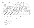
- FIG. 1 shows a cross-sectional view of a magnetic wiring circuit board according to an embodiment of the present invention and a partially enlarged cross-sectional view thereof.
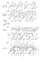
- 2A to 2D are manufacturing process diagrams of the magnetic wiring circuit board shown in FIG. 1.
- FIG. 2A is a fourth process (first process) for forming a wiring base
- FIG. 2B is a process for forming a plating layer.
- FIG. 2C shows a second step of forming the second insulating layer
- FIG. 2D shows a third step of forming the magnetic layer.
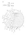
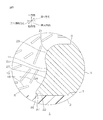
- FIG. 3 is a cross-sectional view for explaining a circular arc of a circle passing through the curved surface of the first corner in FIG.
- FIG. 3 is a cross-sectional view for explaining a circular arc of a circle passing through the curved surface of the first corner in FIG.
- FIG. 1 shows a cross-sectional view of a magnetic wiring circuit board according to an embodiment of the present invention and a partially enlarged cross-sectional view
- FIG. 4 shows a cross-sectional view of a modification of the magnetic wiring circuit board in FIG. 1 (a mode without the second insulating layer).
- FIG. 5 is a partially enlarged cross-sectional view of a modified example of the magnetic wiring circuit board shown in FIG. 1 (an aspect in which the plating layer is thin and the wiring side surface does not have a constricted portion).
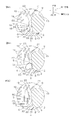
- FIG. 6 is a partially enlarged cross-sectional view of a modified example of the magnetic wiring circuit board (an aspect in which the second corner portion has the second constricted portion) in FIG. 7A to 7C are partially enlarged cross-sectional views of a magnetic wiring circuit board of Comparative Example 1 (Comparative Example in which the second corner portion has a vertical surface).
- FIG. 1 Comparative Example in which the second corner portion has a vertical surface.
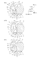
- FIG. 7A shows an aspect in which magnetic particles are broken
- FIG. FIG. 7C shows a mode in which voids are generated
- 8A to 8C are partially enlarged cross-sectional views of the magnetic wiring circuit board of Comparative Example 2 (Comparative Example in which the second corner portion has the second constricted portion), and FIG. FIG. 8B shows a mode in which particle-free portions are generated, and FIG. 8C shows a mode in which voids are generated.
- a magnetic wired circuit board 1 which is an embodiment of the wired circuit board of the present invention will be described with reference to FIG.
- the magnetic wired circuit board 1 has a thickness direction one surface and the other surface facing each other in the thickness direction, and has a sheet shape extending in the surface direction (direction orthogonal to the thickness direction).
- the magnetic wiring circuit board 1 includes a first insulating layer 2 that is an example of an insulating layer, a wiring portion 3 that is an example of a wiring, a second insulating layer 4, and a magnetic layer 5.
- the first insulating layer 2 has a sheet shape extending in the surface direction.
- the first insulating layer 2 is a support material that supports the wiring portion 3 described below, and by extension, is also a support layer that supports the magnetic wiring circuit board 1.
- the first insulating layer 2 has a first insulating surface 7 that is one surface in the thickness direction and a second insulating surface 8 that is the other surface. Each of the first insulating surface 7 and the second insulating surface 8 is a flat surface along the surface direction.
- the first insulating layer 2 has flexibility.
- the material of the first insulating layer 2 examples include resins such as polyimide resin, polyester resin, and acrylic resin.
- the first insulating layer 2 may be either a single layer or a multilayer.
- the thickness of the 1st insulating layer 2 is not specifically limited, For example, they are 1 micrometer or more and 1000 micrometers or less.
- the wiring portion 3 is a cut surface cut along the thickness direction and the first direction (corresponding to the left-right direction in FIG. 1 and included in the surface direction) on the first insulating surface 7 of the first insulating layer 2.
- a plurality are arranged in the first direction at intervals.
- the shape of the wiring part 3 in plan view is not particularly limited, and includes, for example, a loop shape (such as a coil shape).
- the wiring portion 3 includes a first wiring surface 9 that is one surface in the thickness direction and is disposed opposite to the first insulating surface 7 of the first insulating layer 2 with a space on one side in the thickness direction, and the first insulating layer 2.
- the first wiring surface 9 is a flat surface along the first direction.
- the second wiring surface 10 is disposed to face the first wiring surface 9 with a gap in the thickness direction, and is a flat surface parallel to the first wiring surface 9.
- the wiring side surface 11 extends along the thickness direction. Two wiring side surfaces 11 are provided in one wiring part 3. The two wiring side surfaces 11 are arranged to face each other (facing each other) with a space therebetween in the first direction.
- the wiring portion 3 has a first corner portion 21 and a second corner portion 22 as an example of a corner portion.
- the first corner portion 21 is a ridge line portion (first ridge line portion) formed by the first wiring surface 9 and the wiring side surface 11 in the wiring portion 3. Specifically, the first corner portion 21 is formed over both end portions in the first direction of the first wiring surface 9 and one end portion in the thickness direction of the wiring side surface 11 continuous therewith. Two first corner portions 21 are formed for each wiring portion 3.
- angular part 21 has a substantially curved shape in the cross-section (thickness direction and the cut surface in alignment with a 1st direction) view.
- the first corner 21 has a curved surface (specifically, a substantially arcuate surface) 23 that swells outward in the first direction and toward one side in the thickness direction.
- the center CP of the circle C forming the curved surface 23 is located, for example, inside the wiring portion 3.
- the radius (curvature radius) R of the circle C forming the curved surface 23 is, for example, 5 ⁇ m or more, preferably 9 ⁇ m or more, more preferably 15 ⁇ m or more, further preferably 20 ⁇ m or more, and for example, 30 ⁇ m or less. is there. If the radius of curvature R of the curved surface 23 is equal to or greater than the above lower limit, the curved surface 23 can be made gentle, and the second insulating layer 4 described below can be more reliably formed with a sufficient thickness T. . In addition, the magnetic particles 18 (described later) can be reliably oriented along the curved surface 23 in the second insulating layer 4 facing the first corner 21.
- the magnetic layer 5 can be filled in the thickness direction central portion 50 (described later) of the wiring side surface 11 without a void.
- the central angle ⁇ of the curved surface 23 is an angle formed by a line segment connecting one end of the arc and the center CP and a line segment connecting the other end of the arc and the center CP, and is, for example, less than 180 degrees.
- the central angle ⁇ of the curved surface 23 is, for example, 45 degrees or more, preferably 60 degrees or more, more preferably 80 degrees or more, and for example, 150 degrees or less, preferably 135 degrees. Below, more preferably, it is 120 degrees or less. If the central angle ⁇ of the curved surface 23 is equal to or greater than the above lower limit, the length of the curved surface 23 can be increased, so that the magnetic particles 18 can surely follow (orient) the curved surface 23.
- the central angle ⁇ of the curved surface 23 is equal to or greater than the above lower limit, the length of the curved surface 23 can be increased, so that the magnetic particles 18 can surely follow (orient) the curved surface 23. If the central angle ⁇ of the curved surface 23 is equal to or less than the above upper limit, the magnetic layer 5 can be filled without a gap (void) in the thickness direction central portion 50 (described later) of the wiring side surface 11.
- the center CP is determined so that the circle C forming the curved surface 23 forms an arc that passes through the curved surface 23 at the maximum (overlapping) at the first corner portion 21; It is defined as a circle C based on the center CP.
- a center CP ′ that forms an arc that slightly (minimally) passes (overlaps) the curved surface 23 at the first corner 21 is determined, and a circle based on the center CP ′ is determined. Not C '.
- the second corner portion 22 is a ridge line portion (second ridge line portion) formed by the second wiring surface 10 and the wiring side surface 11 in the wiring portion 3. Specifically, the second corner portion 22 is formed over each of both end portions in the first direction of the second wiring surface 10 and the other end portion in the thickness direction of the wiring side surface 11 continuous therewith. Two second corner portions 22 are formed for each wiring portion 3.
- Each of the two second corner portions 22 is disposed on the other side in the thickness direction with respect to each of the two first corner portions 21.
- the second corner portion 22 is a second sharpened portion that is sharpened toward the first direction outer side (the first direction outer side obliquely in the first direction other side).
- the second corner 22 has an inclined surface 24 and a flat surface 26 (partitioned by).
- the inclined surface 24 has a tapered surface 27 as a main part.
- the inclined surface 24 comprises only the tapered surface 27.
- the inclined surface 24 is continuous from the central portion 50 in the thickness direction of the wiring side surface 11 (specifically, the vicinity between the central portion and the other end portion) 50 and faces the outside in the first direction.
- the two inclined surfaces 24 corresponding to the two second corner portions 22 are disposed to face each other (facing each other) in the first direction.
- the tapered surface 27 is inclined with respect to the thickness direction and the first direction. That is, the tapered surface 27 is inclined with respect to the thickness direction and the first direction, and is inclined to the outside in the first direction as it goes to the other side in the thickness direction (first inclination direction) (shown together with the enlarged view).
- first inclination direction shown together with the enlarged view.
- Direction arrow The two taper surfaces 27 corresponding to the two inclined surfaces 24 are two taper surfaces (an example of a part) which become longer as the distance between them approaches the other side in the thickness direction.
- the taper surface 27 extends from the central portion 50 in the thickness direction of the wiring side surface 11 (specifically, between the central portion and the other end portion) 50 to both edges in the first direction of the second wiring surface 10 (first As it goes to the first insulating surface 7) of the insulating layer 2, it inclines so as to spread outwardly in the first direction.
- the taper ratio (first direction length / thickness direction length) obtained by dividing the length in the first direction by the length in the thickness direction of the tapered surface 27 is, for example, 0.001 or more, preferably 0.01 or more. More preferably, it is 0.1 or more, for example, 1.0 or less, preferably 0.75 or less.
- the flat surface 26 is a plane that extends straight from the other end on the other side in the thickness direction of the inclined surface 24 toward the inside in the first direction.
- the flat surface 26 corresponds to both edges of the second wiring surface 10 in the first direction.
- the flat surface 26 is in contact with the first insulating surface 7.
- the inclined surface 24 of the second corner portion 22 and the curved surface 23 of the first corner portion 21 are disposed, for example, with a central portion 50 in the thickness direction of the wiring side surface 11 being separated.
- the second corner portion 22 may have the same shape as a second sharpened portion 45 (see FIG. 2A) in the wiring base portion 36 to be described later.
- the wiring side surface 11 is a portion facing the first direction outside of the curved surface 23 of the first corner portion 21, a portion in the thickness direction center portion 50, and a portion facing the first direction outside of the inclined surface 24 of the curved surface 23. Are provided continuously.
- Each of the central portions 50 in the thickness direction of the two wiring side surfaces 11 has a shape constricted toward the inside in the first direction.
- the wiring side surface 11 has a shape (necked portion) in which the length between them is the shortest in the central portion in the first direction.
- the wiring part 3 is provided with the wiring base part 36 and the plating layer 30 formed in the thickness direction one surface and both side surfaces, for example, as shown with the virtual line of FIG. 2B.
- Examples of the material of the wiring part 3 include conductors such as metals such as copper, nickel, gold, and solder, and alloys of these metals, preferably copper.
- the thickness of the wiring part 3 is the length between the first wiring surface 9 and the second wiring surface 10, specifically, for example, 10 ⁇ m or more, preferably 30 ⁇ m or more, and, for example, 500 ⁇ m or less.
- the thickness is preferably 250 ⁇ m or less.
- the width of the wiring part 3 is, for example, 20 ⁇ m or more, preferably 50 ⁇ m or more, for example, 2000 ⁇ m or less, preferably 1000 ⁇ m, as the distance between the edges in the first direction of the two first corners 21 facing each other. It is as follows.
- the interval between the adjacent wiring portions 3 is, for example, 20 ⁇ m or more as the interval between the first direction edges of the first corner portions 21 adjacent to each other across the second insulating layer 4 (described later) and the magnetic layer 5 (described later).
- the thickness is preferably 50 ⁇ m or more, and for example, 1000 ⁇ m or less, preferably 500 ⁇ m or less.
- the ratio (thickness / width) of the thickness of the wiring part 3 to the width of the wiring part 3 is, for example, 0.005 or more, preferably 0.03 or more, and for example, 25 or less, preferably 5 or less. It is.
- the ratio (thickness / interval) of the thickness of the wiring part 3 to the distance between adjacent wiring parts 3 is, for example, 0.01 or more, preferably 0.06 or more, and for example, 25 or less, preferably 5 or less.
- the ratio (width / interval) of the width of the wiring part 3 to the distance between adjacent wiring parts 3 is, for example, 0.02 or more, preferably 0.01 or more, and for example, 100 or less, preferably , 20 or less.
- the wiring unit 3 is provided in the printed circuit board preparation body 6 together with the first insulating layer 2 described above. That is, the printed circuit board preparation 6 does not include the second insulating layer 4 and the magnetic layer 5 described below, but includes the first insulating layer 2 and the wiring portion 3. Preferably, the printed circuit board preparation 6 includes only the first insulating layer 2 and the wiring portion 3.
- a plurality of second insulating layers 4 are provided corresponding to the plurality of wiring portions 3.
- the second insulating layer 4 is formed in a thin film shape along the first wiring surface 9 and the wiring side surface 11 (including the curved surface 23 and the inclined surface 24) of the wiring part 3.
- the second insulating layer 4 is disposed at a distance from the fourth insulating surface 13 in contact with the first wiring surface 9 and the wiring side surface 11 and one side in the thickness direction of the fourth insulating surface 13 or outside in the first direction. 3 insulating surfaces 12.
- the fourth insulating surface 13 has a shape corresponding to the first wiring surface 9 and the wiring side surface 11 (specifically, the same).
- the third insulating surface 12 has a shape that follows the fourth insulating surface 13 so that the thickness T of the second insulating layer 4 is ensured.
- the third insulating surface 12 has a shape parallel to the fourth insulating surface 13.
- the second insulating layer 4 is, for example, an electrodeposition layer (described later), a coating layer (described later), and preferably an electrodeposition layer.
- the second insulating layer 4 is, for example, relatively soft (in particular, has a property of being soft in the hot press in the third step described later (see FIG. 2D)), but does not have magnetism.
- examples of the material of the second insulating layer 4 include a resin that does not contain the magnetic particles 18 (described in detail later in the magnetic layer 5).
- the resin of the second insulating layer 4 is preferably a resin that is ionic in water, and specifically includes acrylic resins, epoxy resins, polyimide resins, and mixtures thereof.
- the thickness T of the second insulating layer 4 is relatively thin, and the average thickness thereof is, for example, 20 ⁇ m or less, preferably 15 ⁇ m or less, more preferably 10 ⁇ m or less, further preferably 7.5 ⁇ m or less, and particularly preferably It is 5 ⁇ m or less, most preferably 3 ⁇ m or less, and for example, 0.1 ⁇ m or more, preferably 0.5 ⁇ m or more, more preferably 1 ⁇ m or more.
- the thickness T of the second insulating layer 4 is thinner than the above upper limit, the effective magnetic permeability of the magnetic layer 5 described below can be improved and the inductance of the magnetic wiring circuit board 1 can be increased.
- the first corner 21 of the wiring part 3 has a substantially curved shape, so that the thickness T of the second insulating layer 4 is excessively thin. By suppressing this, it is possible to prevent the second insulating layer 4 from penetrating the magnetic particles 18, and to ensure the insulation of the second insulating layer 4.
- the thickness T1 of the portion covering the first corner 21 in the second insulating layer 4 is a portion other than the first corner 21 described above in the second insulating layer 4 (for example, the central portion 50 in the thickness direction of the wiring side surface 11). And / or the thickness T0 of the portion covering the first wiring surface 9 in the first direction center) or slightly smaller than the thickness T0 is allowed.
- the ratio (T1 / T0) of the thickness T1 of the portion covering the first corner 21 to the thickness T0 of the portion covering the portion other than the first corner 21 is, for example, 1 or less, Preferably, it is less than 1, more preferably 0.95 or less, still more preferably 0.9 or less, and for example 0.7 or more, preferably 0.8 or more.
- the thickness T1 of the portion covering the first corner 21 in the second insulating layer 4 is, for example, 0.5 ⁇ m or more, preferably 1 ⁇ m or more, and for example, 10 ⁇ m or less, preferably 7 ⁇ m or less.
- the thickness T0 of the portion covering the other portion in the second insulating layer 4 is, for example, 0.52 ⁇ m or more, preferably 1.04 ⁇ m or more, and, for example, 14.49 ⁇ m or less, preferably 10.14 ⁇ m. It is as follows.
- the average thickness of the second insulating layer 4 is calculated by dividing the above-described thicknesses T1 and T0 by the area ratio.
- the magnetic layer 5 is provided to the printed circuit board preparation 6 in order to improve the inductance of the magnetic wired circuit board 1.
- the magnetic layer 5 has a sheet shape extending in the plane direction.
- the magnetic layer 5 has the wiring portion 3 embedded through the second insulating layer 4. Specifically, the magnetic layer 5 covers the first wiring surface 9 and the wiring side surface 11 (including the curved surface 23 and the inclined surface 24) of the wiring part 3 via the second insulating layer 4. The magnetic layer 5 covers the exposed surface 16 exposed from the second insulating layer 4 on the first insulating surface 7 of the first insulating layer 2.
- the magnetic layer 5 has a first magnetic surface 14 and a second magnetic surface 15.
- the first magnetic surface 14 is arranged on one side in the thickness direction with respect to the third insulating surface 12 of the second insulating layer 4 with an interval.
- the first magnetic surface 14 is exposed on one side in the thickness direction.
- the first magnetic surface 14 is disposed between a plurality of convex portions 28 that protrude toward one side in the thickness direction corresponding to the plurality of wiring portions 3 and the convex portions 13 that are adjacent to each other. And a recess 29 that sinks toward the other side in the thickness direction.
- the second magnetic surface 15 is arranged at an interval on the other side in the thickness direction of the first magnetic surface 14.
- the second magnetic surface 15 is in continuous contact with the third insulating surface 12 and the exposed surface 16.
- the magnetic layer 5 contains, for example, magnetic particles 18.
- examples of the material for the magnetic layer 5 include a magnetic composition containing the magnetic particles 18 having an aspect ratio of 2 or more and the resin component 19.
- Examples of the magnetic particles 18 include soft magnetic particles 18 such as Sendust.
- Examples of the shape of the magnetic particles 18 include a flat shape (plate shape) having a small thickness and a wide surface, such as a needle shape.
- the aspect ratio of the magnetic particles is 2 or more, preferably 5 or more, more preferably 10 or more, still more preferably 20 or more, and 100 or less.
- the flatness (flatness) when the magnetic particles 18 are flat is, for example, 8 or more, preferably 15 or more, and for example, 500 or less, preferably 450 or less.
- the flatness is, for example, an aspect ratio obtained by dividing the average particle diameter (average length) of the magnetic particles 18 by the average thickness of the magnetic particles 18.
- the content ratio of the magnetic particles 18 in the magnetic layer 5 is, for example, 50% by volume or more, preferably 55% by volume or more, and, for example, 95% by volume or less, preferably 90% by volume or less. It is.
- thermosetting resins such as an epoxy resin composition containing an epoxy resin, a curing agent, and a curing accelerator.
- Such magnetic compositions are described in, for example, JP-A-2017-005115, JP-A-2015-092543.
- the thickness of the magnetic wiring circuit board 1 is, for example, 30 ⁇ m or more, preferably 50 ⁇ m or more, and, for example, 1000 ⁇ m or less, preferably 800 ⁇ m or less as its maximum thickness (thickness corresponding to the convex portion 28). .
- This manufacturing method includes a first step (see FIGS. 2A and 2B) as an example of a step of preparing the first insulating layer 2 and the wiring portion 3, and a second step of forming the second insulating layer 4 (FIG. 2C). And a third step (see FIG. 2D) as an example of a step of forming the magnetic layer 5.
- a printed circuit board preparation 6 including the first insulating layer 2 and the wiring part 3 is prepared.
- the first step includes a step of preparing the first insulating layer 2 (see FIG. 2A), a fourth step of forming the wiring base 36 (see FIG. 2A), and a fifth step of forming the plating layer 30 (FIG. 2B). See).
- the wiring base 36 is formed on the first insulating surface 7 of the first insulating layer 2 by a conductor patterning method such as a subtractive method or an additive method.
- the wiring base 36 In order to form the wiring base 36 by the subtractive method, first, a laminated body (not shown) composed of the first insulating layer 2 and the conductor layer (metal layer) is prepared, and subsequently, one side in the thickness direction of the conductor layer. In addition, an etching resist is formed in the same pattern as the wiring base 36. Next, the conductor base exposed from the etching resist is patterned by, for example, etching such as wet etching or dry etching to form the wiring base 36. Preferably, the wiring base 36 is formed by wet etching. Thereafter, the etching resist is removed by, for example, peeling.
- the wiring base 36 In order to form the wiring base 36 by the additive method, first, a conductive thin film (seed film) is formed on the first insulating surface 7 of the first insulating layer 2, and then the wiring base is formed on one surface in the thickness direction of the conductive thin film. A plating resist having a pattern opposite to that of 36 is formed. Next, the wiring base 36 is formed on the conductive thin film exposed from the plating resist by plating. Thereafter, the plating resist and the corresponding conductive thin film are removed.
- seed film a conductive thin film
- the conductor patterning method is preferably a subtractive method. If it is a subtractive method, compared with an additive method, the wiring base part 36 which has a thick thickness can be formed rapidly.
- the wiring base portion 36 is formed by the subtractive method, the first sharpened portion 25 is formed in the wiring base portion 36.
- the second insulating layer 4 is caused by the first sharpened portion 25.
- the thinning can be solved by the plating layer 30 formed in the fifth step described later.
- the wiring base 36 is a base (base) for forming the wiring part 3 and forms the wiring part 3 together with a plating layer 30 described later. That is, the wiring part 3 is not configured only by the wiring base part 36 shown in FIG. 2A.
- the wiring base portion 36 includes a first sharpened portion 25 corresponding to the first corner portion 21, a base central side surface 51 corresponding to the thickness direction central portion 50, and a second sharpened portion 45 corresponding to the second corner portion 22. .
- the first sharpened portion 25 is a ridge line portion formed by one side surface and the side surface in the thickness direction of the wiring base portion 36.
- the first sharpened portion 25 sharply sharpens toward the one side in the first direction outer side obliquely in the first direction.
- the angle (angle formed by the ends of the first wiring surface 9 and the wiring side surface 11) ⁇ 1 at the first sharpened portion 25 is, for example, 135 degrees or less, preferably 120 degrees or less, more preferably 90 degrees or less. Yes, for example, 30 degrees or more, preferably 45 degrees or more.
- the second sharpened portion 45 is a ridge line portion formed by the other side surface and the side surface in the thickness direction of the wiring base portion 36.
- the second sharpened portion 45 sharply sharpens toward the other side of the first direction outer side obliquely in the first direction.
- the angle (angle formed by the ends of the second wiring surface 10 and the wiring side surface 11) ⁇ 2 at the second sharpened portion 45 is, for example, 35 degrees or more, preferably 45 degrees or more, more preferably more than 80 degrees. For example, it is 150 degrees or less, preferably 135 degrees or less.
- the base central side surface 51 is a connecting surface that connects the first sharpened portion 25 and the second sharpened portion 45 in the thickness direction.
- the material of the wiring base portion 36 is the same as the material of the wiring portion 3 described above.
- the plating layer 30 is then formed on the wiring base 36 as shown in FIG. 2B.
- the material of the plating layer 30 is appropriately selected from the materials of the wiring base 36 and is preferably the same as the material of the wiring base 36.
- the plating layer 30 is formed by plating.
- plating examples include electrolytic plating and electroless plating.
- electrolytic plating more preferably, electrolytic copper plating is used.
- the plating layer 30 is laminated
- a first covering portion 31 as an example of a covering portion that grows (plating growth) toward one side in the thickness direction and the outside in the first direction is deposited on the first sharpened portion 25.
- the first covering portion 31 forms the first corner portion 21 having the curved surface 23.
- the wiring base portion 36 other than the first sharpened portion 25 (the portion including the second sharpened portion 45 and the central portion 50 in the thickness direction)
- it grows (plating growth) toward one side in the thickness direction or outward in the first direction.
- coated part 32 precipitates.
- the second covering portion 32 forms one side surface and both side surfaces of the wiring base portion 36 (however, the portion excluding the first corner portion 21 and including the thickness direction central portion 50 and the inclined surface 24). .
- the plating layer 30 includes a first covering portion 31 and a second covering portion 32.
- the plating layer 30 includes only the first covering portion 31 and the second covering portion 32.
- the first covering portion 31 is formed by plating growth of the plating component from the first sharpened portion 25 in a substantially radial shape in sectional view (excluding the direction inside the first sharpened portion 25). Therefore, the first covering part 31 has a curved surface 23.
- the second covering portion 32 is planar in a direction orthogonal to each surface, specifically, in one thickness direction of the wiring base portion 36 toward the upper side in the thickness direction.
- the plating component grows on the both sides of the wiring base portion 36 (including the side surface of the second sharpened portion 45), and the plating component grows in a planar shape toward both outer sides in the first direction. Therefore, the 2nd coating
- coated part 32 does not have the above-mentioned curved surface 23, but has the 1st wiring surface 9 and the wiring side surface 11 (The thickness direction center part 50 is included, but the curved surface 23 is excluded).
- the second covering portion 32 includes the second corner portion 22, and the second corner portion 22 includes the inclined surface 24 based on the above-described plating growth.
- the thickness (growth thickness or plating thickness) of the first covering portion 31 is preferably thicker than that of the second covering portion 32. If the plating is electrolytic plating, the current density at the first sharpened portion 25 is higher than the current density of the wiring base 36 other than the first sharpened portion 25. Therefore, the plating growth of the first covering portion 31 is faster than the plating growth of the second covering portion 32, and thus the thickness of the first covering portion 31 is thicker than the thickness of the second covering portion 32.
- the thickness of the plating layer 30 is appropriately set according to the growth rate of plating and the plating time. These include, for example, metal (conductor) concentration and temperature in the plating solution used in plating, for example, if the plating is electrolytic plating, current density, distance between electrodes, degree of agitation in bath (speed), copper sulfate Concentration, sulfuric acid concentration, chloride ion concentration, type and amount of additives (leveler, brightener, polymer), for example, if the plating is electroless plating, the type and amount of catalyst attached to the surface of the wiring base 36 It sets suitably by these.
- metal (conductor) concentration and temperature in the plating solution used in plating for example, if the plating is electrolytic plating, current density, distance between electrodes, degree of agitation in bath (speed), copper sulfate Concentration, sulfuric acid concentration, chloride ion concentration, type and amount of additives (leveler, brightener, polymer), for example, if the plating
- a boundary indicated by an imaginary line is shown between the wiring base 36 and the plating layer 30, but the material of the plating layer 30 is the same as the material of the wiring base 36. If present, the above-mentioned boundary is obscured or does not exist (not observed).
- the first covering portion 31 is formed by the above-described plating, and thus has the curved surface 23 described above.
- the second covering portion 32 has an inclined surface 24.
- the second insulating layer 4 is subsequently formed on the wiring circuit board preparation 6 described above. Specifically, the second insulating layer 4 covers the first wiring surface 9 and the wiring side surface 11 of the wiring part 3.
- Examples of the method for forming the second insulating layer 4 include electrodeposition (electrodeposition coating), for example, coating such as printing.
- the printed circuit board preparation 6 (the magnetic wiring circuit board 1 being manufactured) is immersed in an electrodeposition liquid containing a resin (preferably an electrodeposition paint), and then a current is applied to the wiring section 3.
- a resin preferably an electrodeposition paint
- a resin film is deposited on the first wiring surface 9 and the wiring side surface 11 of the wiring part 3.
- the coating is dried if necessary.
- the 2nd insulating layer 4 is formed as an electrodeposition layer.
- the second insulating layer 4 (electrodeposition layer) is heated and cured by baking.
- a coating is applied to the first wiring surface 9 and the wiring side surface 11 of the wiring portion 3 with a varnish containing a resin through a screen (screen printing). Thereafter, the coating is dried.
- the method for forming the second insulating layer 4 is preferably electrodeposition. If it is electrodeposition, the thickness T of the second insulating layer 4 can be made thin (however, the thickness can be set to a level that can ensure the insulation of the second insulating layer 4). Moreover, if it is electrodeposition, the 2nd insulating layer 4 can expose the exposed surface 16 reliably, Therefore, between the adjacent wiring parts 3, in the following 3rd process, the magnetic layer 5 is made into thickness. Since it can arrange
- the magnetic layer 5 is then formed on the printed circuit board preparation 6 as shown in FIG. 2D. Specifically, the first wiring surface 9 and the wiring side surface 11 of the wiring part 3 are covered with the magnetic layer 5 via the second insulating layer 4.
- the magnetic sheet 17 is prepared.
- the magnetic sheet 17 is formed into a sheet shape from a magnetic composition containing the above-described magnetic particles and a resin component (preferably a B-stage thermosetting resin).
- the magnetic particles 18 are oriented (arranged) in the surface direction of the magnetic sheet 17 (direction perpendicular to the thickness direction).
- the magnetic sheet 17 is hot pressed against the second insulating layer 4 of the printed circuit board preparation 6.
- the magnetic sheet 17 is disposed on one side in the thickness direction of the printed circuit board preparation body 6, and the magnetic sheet 17 is hot pressed against one surface in the thickness direction of the printed circuit board preparation body 6.
- the magnetic sheet 17 embeds the wiring part 3 through the second insulating layer 4. Specifically, the magnetic sheet 17 covers the first wiring surface 9 of the second insulating layer 4 with the second insulating layer 4 interposed therebetween, and between the adjacent wiring portions 3 (opposed to the exposed surface 16). (Part) enters (sinks) and fills the part (part).
- the orientation direction (specifically, the surface direction) of the magnetic particles 18 facing the first wiring surface 9 of the wiring part 3 does not vary. Further, in the magnetic sheet 17 before and after hot pressing, the orientation direction (specifically, the surface direction) of the magnetic particles 18 facing the exposed surface 16 does not vary.
- the orientation direction (specifically, the surface direction) of the magnetic particles 18 facing the first corner portion 21 is the direction along the curved surface 23 (that is, the other side in the thickness direction).
- the first direction is inclined outward. That is, the magnetic particles 18 described above are oriented along the curved surface 23.
- the orientation direction (specifically, the surface direction) of the magnetic particles 18 facing the second corner portion 22 is the direction along the inclined surface 24 (that is, the other side in the thickness direction).
- the first direction is inclined outward. That is, the magnetic particles 18 described above are oriented along the inclined surface 24.
- the orientation direction (specifically, the plane direction) of the magnetic particles 18 facing the first corner portion 21 and the second corner portion 22 on the wiring side surface 11 is the thickness direction. It fluctuates in the direction along. That is, the above-described magnetic particles 18 are oriented along the thickness direction.
- the magnetic sheet 17 is formed (molded) as the magnetic layer 5 covering the wiring portion 3 and having the convex portion 28 and the concave portion 29 via the second insulating layer 4.
- the magnetic particles 18 oriented as described above in the magnetic layer 5 form a smooth magnetic path surrounding the wiring portion 3.
- the magnetic wired circuit board 1 including the wired circuit board preparation 6 and the magnetic layer 5 is obtained.
- the magnetic wired circuit board 1 is preferably composed only of the wired circuit board preparation 6 and the magnetic layer 5.
- the magnetic layer 5 contains a B-stage thermosetting resin
- the magnetic layer 5 is made C-staged (completely cured) by heating, for example, if necessary.
- the magnetic wiring circuit board 1 is used for, for example, wireless power transmission (wireless power feeding and / or wireless power receiving), wireless communication, sensors, passive components, and the like.
- the first corner portion 21 of the wiring 3 has a substantially curved shape. Therefore, in the magnetic layer 5 covering the first corner portion 21, the magnetic particles 18 are formed in the first corner portion 21. Can be oriented along the curved shape.
- the magnetic particles 18 can be oriented along the second corners 22.
- the second corner portion 22 has a vertical surface 33 formed vertically, and as shown in FIG. 8, as it goes toward the first insulating surface 7,
- Comparative Example 2 having a second taper portion (second constriction portion) 34 that narrows inward in the first direction, in the magnetic layer 5, as shown in FIGS. 7A and 8A, magnetic particles 18 is damaged (broken), or as shown in FIGS. 7B and 8B, the magnetic particle 18 has a non-existent particle-free portion 55, and further, as shown in FIGS. 7C and 8C.
- voids 56 portions where the magnetic particles 18 and the resin component 19 do not exist are generated in the magnetic layer 5.
- the magnetic particles 18 are oriented in the first direction included in the plane direction in the magnetic layer 5 covering the first wiring surface 9 of the wiring 3.
- the magnetic layer 5 covering the wiring side surface 11 of the wiring 3 is oriented in the thickness direction
- the magnetic layer 5 covering the first corner portion 21 is oriented in the first inclined direction
- the second The magnetic layer 5 covering the corner portion 22 is also oriented in the first tilt direction. Further, the damage of the magnetic particles 18, the generation of the particle nonexistent portion 55, and the generation of the void 56 can be suppressed.
- the effective magnetic permeability around the wiring 3 can be improved.
- the magnetic wiring circuit board 1 has a high inductance.
- the first corner 21 since the radius of curvature R of the first corner 21 is 9 ⁇ m or more, the first corner 21 has a curved surface 23 that is a gentle arc surface. Therefore, in the magnetic layer 5 facing the first corner portion 21, the magnetic particles 18 can be more reliably oriented along the curved surface 23 (arc surface).
- the magnetic sheet containing the magnetic particles 18 oriented in the plane direction is hot pressed against the wiring 3. Therefore, in the magnetic layer 5 covering the first wiring surface 9 of the wiring 3, the magnetic particles 18 are oriented in the first direction included in the plane direction, and in the magnetic layer 5 covering the wiring side surface 11 of the wiring 3.
- the magnetic layer 5 that is oriented in the thickness direction and covers the first corner 21 it is oriented in the first tilt direction and in the magnetic layer 5 that covers the second corner 22, the first tilt Can be oriented in the direction.
- the effective magnetic permeability around the wiring 3 can be improved.
- the magnetic wiring circuit board 1 having a high inductance can be manufactured.
- the magnetic wiring circuit board 1 includes the second insulating layer 4.
- the second insulating layer 4 does not include the first insulating layer. 2
- wiring 3 and magnetic layer 5 can be provided.
- the magnetic wiring circuit board 1 is preferably composed of only the first insulating layer 2, the wiring 3 and the magnetic layer 5.
- the printed circuit board 6 does not include the second insulating layer 4 but includes the first insulating layer 2 and the wiring 3.
- the printed circuit board 6 preferably includes only the first insulating layer 2 and the wiring 3.
- the magnetic layer 5 embeds the wiring 3 directly. That is, the second magnetic surface 15 of the magnetic layer 5 is in direct contact with the first wiring surface 9 of the wiring 3 without passing through the second insulating layer 4 (see FIG. 1).
- one wiring 3 has a constricted portion in which the length between two wiring side surfaces 11 is the shortest at the center in the first direction.
- the wiring 3 can also have a wiring side surface 11 that does not have a constricted portion.
- FIG. 1 in one embodiment shows an example in which the plating layer 30 is relatively thick. As shown in FIG. 5, this modification is an example in which the thickness of the plating layer 30 is thinner than that of the embodiment.
- the radius of curvature R of the circle C forming the curved surface 23 is relatively small, and the center angle ⁇ is also small.
- the radius of curvature R is, for example, less than 9 ⁇ m, further 5 ⁇ m or less, further 2 ⁇ m or less, and the central angle ⁇ is less than 110 degrees.
- the inclined surface 24 includes only a tapered surface 27.
- the second edge in the thickness direction of the inclined surface 24 may be the second curved surface 35.
- the second curved surfaces 35 adjacent to each other are constricted portions 37 in which the length between the second curved surfaces 35 becomes shorter toward the first insulating surface 7.
- Magnetic circuit board is used for wireless communication and electric power transmission.
Landscapes
- Engineering & Computer Science (AREA)
- Power Engineering (AREA)
- Microelectronics & Electronic Packaging (AREA)
- Manufacturing & Machinery (AREA)
- Computer Networks & Wireless Communication (AREA)
- Coils Or Transformers For Communication (AREA)
- Structure Of Printed Boards (AREA)
- Manufacturing Cores, Coils, And Magnets (AREA)
- Soft Magnetic Materials (AREA)
- Parts Printed On Printed Circuit Boards (AREA)
- Shielding Devices Or Components To Electric Or Magnetic Fields (AREA)
Abstract
磁性配線回路基板は絶縁層と、絶縁層の厚み方向一方面に配置される配線であって、絶縁層の厚み方向一方面に間隔を隔てて対向配置される厚み方向一方面、絶縁層の厚み方向一方面に接触する厚み方向他方面、厚み方向一方面および前記厚み方向他方面の両端縁を連結する側面を有する配線と、アスペクト比が2以上である形状を有する磁性粒子を含有し、配線を埋設する磁性層とを備える。配線は、厚み方向一方面および側面によって形成され、略湾曲形状を有する第1角部と、厚み方向他方面および側面によって形成され、互いに向かい合う2つの側面間の長さが厚み方向他方面に近づくに従って長くなる部分を有する第2角部とを有する。
Description
本発明は、磁性配線回路基板およびその製造方法に関する。
従来、電力を無線により伝送する無線通信や無線電力伝送に、コイルモジュールが用いられることが知られている。
例えば、コイルパターンと、それを埋設し、扁平形状の磁性粒子を含有する磁性層とを備えるコイルモジュールが提案されている(例えば、下記特許文献1参照。)。
このようなコイルモジュールは、例えば、まず、導体パターンニングによってコイルパターンを形成し、次いで、磁性粒子を含有する磁性シートをコイルパターンに対して熱プレスすることにより得られる。
しかるに、コイルモジュールには、高いインダクタンスが求められる。
しかし、上記したコイルパターンの上面および側面と、下面および側面とには、それぞれ、直角の稜線部が形成されるため、磁性シートを、コイルパターンに対して熱プレスすれば、磁性粒子が、稜線部と対向する磁性シートでは、磁性粒子が、厚み方向または面方向に配向されるのみである。そのため、磁性シートにおいて、配線を囲む滑らかな磁路を形成することができず、上記した高いインダクタンスを得ることができないという不具合がある。
本発明は、高いインダクタンスを有する磁性配線回路基板およびその製造方法を提供する。
本発明(1)は、絶縁層と、前記絶縁層の厚み方向一方面に配置される配線であって、前記絶縁層の前記厚み方向一方面に間隔を隔てて対向配置される厚み方向一方面、前記絶縁層の前記厚み方向一方面に接触する厚み方向他方面、前記厚み方向一方面および前記厚み方向他方面の両端縁を連結する側面を有する前記配線と、アスペクト比が2以上である形状を有する磁性粒子を含有し、前記配線を埋設する磁性層とを備え、前記配線は、前記厚み方向一方面および前記側面によって形成され、略湾曲形状を有する第1角部と、前記厚み方向他方面および前記側面によって形成され、互いに向かい合う2つの前記側面間の長さが前記厚み方向他方面に近づくに従って長くなる部分を有する第2角部とを有する、磁性配線回路基板を含む。
この磁性配線回路基板では、配線の第1角部が、略湾曲形状を有するので、第1角部を被覆する磁性層において、磁性粒子が、第1角部の湾曲形状に沿って配向することができる。
また、この磁性配線回路基板では、第2角部が、互いに向かい合う2つの側面間の長さが厚み方向他方面に近づくに従って長くなる部分を有するので、第2角部を被覆する磁性層において、磁性粒子が、第2角部に沿って配向することができる。
そうすると、磁性粒子は、配線の厚み方向一方面を被覆する磁性層においては、厚み方向に直交する直交方向に配向し、配線の側面を被覆する磁性層においては、厚み方向に配向し、そして、第1角部を被覆する磁性層においては、厚み方向および直交方向に対して傾斜する傾斜方向に配向し、また、第2角部を被覆する磁性層においては、傾斜方向に配向する。
そのため、磁性層において配線を囲む滑らかな磁路を形成することができる。
従って、配線の周囲の実効透磁率を向上させることができる。
その結果、磁性配線回路基板は、高いインダクタンスを有する。
本発明(2)は、前記第1角部の曲率半径Rが、9μm以上である、(1)に記載の磁性配線回路基板を含む。
この磁性配線回路基板では、第1角部の曲率半径Rが、9μm以上であるので、第1角部が緩やかな円弧面を有する。そのため、かかる第1角部に対向する磁性層において、磁性粒子が、円弧面に沿ってより確実に配向することができる。
本発明(3)は、絶縁層と、前記絶縁層の厚み方向一方面に配置される配線であって、前記絶縁層の前記厚み方向一方面に間隔を隔てて対向配置される厚み方向一方面、前記絶縁層の前記厚み方向一方面に接触する厚み方向他方面、前記厚み方向一方面および前記厚み方向他方面の両端縁を連結する側面を有する前記配線とを準備する工程、および、アスペクト比が2以上である形状を有する磁性粒子を含有し、前記配線を埋設するように、磁性層を形成する工程を備え、前記配線は、前記厚み方向一方面および前記側面によって形成され、略湾曲形状を有する第1角部と、前記厚み方向他方面および前記側面によって形成され、互いに向かい合う2つの前記側面間の長さが前記厚み方向他方面に近づくに従って長くなる部分を有する第2角部とを有し、前記磁性層を形成する工程では、前記厚み方向に直交する方向に配向される前記磁性粒子を含有する磁性シートを、前記配線に対して熱プレスする、磁性配線回路基板の製造方法を含む。
この磁性配線回路基板の製造方法によれば、磁性層を形成する工程では、厚み方向に直交する方向に配向される磁性粒子を含有する磁性シートを、配線に対して熱プレスするので、磁性粒子を、配線の厚み方向一方面を被覆する磁性層においては、厚み方向に直交する直交方向に配向させ、配線の側面を被覆する磁性層においては、厚み方向に配向させ、そして、第1角部を被覆する磁性層においては、傾斜方向に配向させ、また、第2角部を被覆する磁性層においては、傾斜方向に配向させることができる。
そのため、磁性層において配線を囲む滑らかな磁路を形成することができる。
従って、配線の周囲の実効透磁率を向上させることができる。
その結果、高いインダクタンスを有する磁性配線回路基板を製造することができる。
本発明の磁性配線回路基板の製造方法により得られる本発明の磁性配線回路基板は、高いインダクタンスを有する。
<一実施形態>
本発明の配線回路基板の一実施形態である磁性配線回路基板1を、図1を参照して説明する。
本発明の配線回路基板の一実施形態である磁性配線回路基板1を、図1を参照して説明する。
磁性配線回路基板1は、厚み方向に互いに対向する厚み方向一方面および他方面を有し、面方向(厚み方向に直交する方向)に延びるシート形状を有する。磁性配線回路基板1は、絶縁層の一例である第1絶縁層2と、配線の一例としての配線部3と、第2絶縁層4と、磁性層5とを備える。
第1絶縁層2は、面方向に延びるシート形状を有する。第1絶縁層2は、次に説明する配線部3を支持する支持材であり、ひいては、磁性配線回路基板1を支持する支持層でもある。第1絶縁層2は、厚み方向一方面である第1絶縁面7および他方面である第2絶縁面8を有する。第1絶縁面7および第2絶縁面8のそれぞれは、面方向に沿う平坦面である。また、第1絶縁層2は、可撓性を有する。
第1絶縁層2の材料としては、例えば、ポリイミド樹脂、ポリエステル樹脂、アクリル樹脂などの樹脂が挙げられる。また、第1絶縁層2は、単層および複層のいずれであってもよい。第1絶縁層2の厚みは、特に限定されず、例えば、1μm以上、1000μm以下である。
配線部3は、第1絶縁層2の第1絶縁面7において、例えば、厚み方向および第1方向(図1における左右方向に相当し、面方向に含まれる方向)に沿って切断した切断面において、第1方向に互いに間隔を隔てて複数配置されている。配線部3の平面視(厚み方向に見たときの)形状としては、特に限定されず、例えば、ループ形状(コイル形状など)を含む。
配線部3は、第1絶縁層2の第1絶縁面7に対して厚み方向一方側に間隔を隔てて対向配置される厚み方向一方面である第1配線面9と、第1絶縁層2の第1絶縁面7に接触する第2配線面10と、第1配線面9および第2配線面10の第1方向両端縁を連結する側面である配線側面11とを備える。
第1配線面9は、第1方向に沿う平坦面である。
第2配線面10は、第1配線面9と厚み方向に間隔を隔てて対向配置されており、第1配線面9に平行する平坦面である。
配線側面11は、厚み方向に沿って延びる。配線側面11は、1つの配線部3に2つ備えられる。2つの配線側面11は、第1方向に互いに間隔を隔てて対向(互いに向かい合って)配置される。
この配線部3は、角部の一例としての第1角部21と、第2角部22とを有する。
第1角部21は、配線部3において、第1配線面9および配線側面11によって形成される稜線部(第1稜線部)である。詳しくは、第1角部21は、第1配線面9の第1方向両端部のそれぞれと、それらに連続する配線側面11の厚み方向一端部にわたって形成される。第1角部21は、1つの配線部3につき、2つ形成されている。
そして、この第1角部21は、断面(厚み方向および第1方向に沿う切断面)視において、略湾曲形状を有する。具体的には、第1角部21は、第1方向外側および厚み方向一方側に向かって膨らむ湾曲面(詳しくは、略円弧面)23を有する。
湾曲面23(円弧面)をなす円Cの中心CPは、例えば、配線部3の内部に位置する。
湾曲面23をなす円Cの半径(曲率半径)Rは、例えば、5μm以上、好ましくは、9μm以上、より好ましくは、15μm以上、さらに好ましくは、20μm以上であり、また、例えば、30μm以下である。湾曲面23の曲率半径Rが上記した下限以上であれば、湾曲面23を緩やかにすることができ、次に説明する第2絶縁層4をより確実に十分な厚みTで形成することができる。また、磁性粒子18(後述)が、第1角部21に対向する第2絶縁層4において、湾曲面23に沿って確実に配向することができる。
第1角部21の曲率半径Rが上記した上限以下であれば、配線側面11の厚み方向中央部50(後述)に隙間(ボイド)なく磁性層5を充填することができる。
湾曲面23の中心角αは、円弧の一端および中心CPを結ぶ線分と、円弧の他端および中心CPを結ぶ線分との成す角度であり、例えば、180度未満である。具体的には、湾曲面23の中心角αは、例えば、45度以上、好ましくは、60度以上、より好ましくは、80度以上であり、また、例えば、150度以下、好ましくは、135度以下、より好ましくは、120度以下である。湾曲面23の中心角αが上記した下限以上であれば、湾曲面23の長さを長くすることができ、そのため、磁性粒子18が湾曲面23に確実に沿う(配向する)ことができる。湾曲面23の中心角αが上記した下限以上であれば、湾曲面23の長さを長くすることができ、そのため、磁性粒子18が湾曲面23に確実に沿う(配向する)ことができる。湾曲面23の中心角αが上記した上限以下であれば、配線側面11の厚み方向中央部50(後述)に隙間(ボイド)なく磁性層5を充填することができる。
なお、図1の拡大図で示すように、湾曲面23をなす円Cは、第1角部21において湾曲面23を最大限通過(重複)する円弧をなすように、中心CPを決定し、かかる中心CPに基づく円Cとして定義される。一方、図3に示すように、第1角部21において湾曲面23をわずかに(最小限で)通過(重複)する円弧をなすような中心CP’を決定し、かかる中心CP’に基づく円C’ではない。
第2角部22は、配線部3において、第2配線面10および配線側面11によって形成される稜線部(第2稜線部)である。詳しくは、第2角部22は、第2配線面10の第1方向両端部のそれぞれと、それらに連続する配線側面11の厚み方向他端部にわたって形成される。第2角部22は、1つの配線部3につき、2つ形成されている。
2つの第2角部22のそれぞれは、2つの第1角部21のそれぞれに対して厚み方向他方側に配置されている。
第2角部22は、第1方向外側(第1方向外側斜め第1方向他方側)に向かって尖る第2尖り部である。第2角部22は、傾斜面24と、平坦面26とを有する(により区画されている。)。
傾斜面24は、テーパ面27を主要部として有する。好ましくは、傾斜面24は、テーパ面27のみからなる。傾斜面24は、配線側面11の厚み方向中央部(詳しくは、中央部と他端部との間付近)50から連続しており、第1方向外側に面している。2つの第2角部22に対応する2つの傾斜面24は、第1方向に互いに対向して(互いに向かい合って)配置されている。
テーパ面27は、厚み方向および第1方向に対して傾斜している。つまり、テーパ面27は、厚み方向および第1方向に対して傾斜し、かつ、厚み方向他方側に進むに従って第1方向外側に傾斜する傾斜方向(第1傾斜方向)(拡大図と併せて示される方向矢印参照)に沿っている。2つの傾斜面24に対応する2つのテーパ面27は、それらの間の長さが厚み方向他方側に近づくに従って長くなる2つのテーパ面(部分の一例)である。具体的には、テーパ面27は、配線側面11の厚み方向中央部(詳しくは、中央部と他端部との間付近)50から、第2配線面10の第1方向両端縁(第1絶縁層2の第1絶縁面7)に向かうに従って、第1方向外側に向かって末広状に広がるように傾斜する。なお、テーパ面27における、第1方向長さを厚み方向長さで除したテーパ比(第1方向長さ/厚み方向長さ)は、例えば、0.001以上、好ましくは、0.01以上、より好ましくは、0.1以上であり、また、例えば、1.0以下、好ましくは、0.75以下である。
平坦面26は、傾斜面24の厚み方向他方側他端縁から第1方向内側に向かって真っ直ぐ延びる平面である。平坦面26は、第2配線面10の第1方向両端縁に相当する。平坦面26は、第1絶縁面7に接触している。
第2角部22の傾斜面24と、第1角部21の湾曲面23とは、例えば、配線側面11の厚み方向中央部50を隔てて配置されている。
なお、この第2角部22は、後述する配線基部36における第2尖り部45(図2A参照)と同一形状であってもよい。
配線側面11は、第1角部21の湾曲面23のうち第1方向外側に面する部分と、厚み方向中央部50と、湾曲面23の傾斜面24のうち第1方向外側に面する部分とを連続して備える。
なお、2つの配線側面11の厚み方向中央部50のそれぞれは、第1方向内側に向かってくびれる形状を有する。具体的には、配線側面11は、それらの間における長さが、第1方向中央部において最短となる形状(くびれ部)を有する。
なお、配線部3は、図2Bの仮想線で示すように、例えば、配線基部36と、その厚み方向一方面および両側面に形成されるめっき層30とを備える。
配線部3の材料としては、例えば、銅、ニッケル、金、はんだなどの金属やそれら金属の合金などの導体が挙げられ、好ましくは、銅が挙げられる。
配線部3の厚みは、第1配線面9および第2配線面10間の長さであって、具体的には、例えば、10μm以上、好ましくは、30μm以上であり、また、例えば、500μm以下、好ましくは、250μm以下である。
配線部3の幅は、互いに向かい合う2つの第1角部21の第1方向における端縁間の距離として、例えば、20μm以上、好ましくは、50μm以上、また、例えば、2000μm以下、好ましくは、1000μm以下である。
隣り合う配線部3間の間隔は、第2絶縁層4(後述)および磁性層5(後述)を隔てて隣り合う第1角部21の第1方向端縁間の間隔として、例えば、20μm以上、好ましくは、50μm以上であり、また、例えば、1000μm以下、好ましくは、500μm以下である。
配線部3の厚みの、配線部3の幅に対する比(厚み/幅)は、例えば、0.005以上、好ましくは、0.03以上であり、また、例えば、25以下、好ましくは、5以下である。配線部3の厚みの、隣り合う配線部3間の間隔に対する比(厚み/間隔)は、例えば、0.01以上、好ましくは、0.06以上であり、また、例えば、25以下、好ましくは、5以下である。配線部3の幅の、隣り合う配線部3間の間隔に対する比(幅/間隔)は、例えば、0.02以上、好ましくは、0.01以上であり、また、例えば、100以下、好ましくは、20以下である。
配線部3の厚みの、配線部3の幅に対する比(厚み/幅)は、例えば、0.005以上、好ましくは、0.03以上であり、また、例えば、25以下、好ましくは、5以下である。配線部3の厚みの、隣り合う配線部3間の間隔に対する比(厚み/間隔)は、例えば、0.01以上、好ましくは、0.06以上であり、また、例えば、25以下、好ましくは、5以下である。配線部3の幅の、隣り合う配線部3間の間隔に対する比(幅/間隔)は、例えば、0.02以上、好ましくは、0.01以上であり、また、例えば、100以下、好ましくは、20以下である。
なお、配線部3は、上記した第1絶縁層2とともに、配線回路基板準備体6に備えられる。つまり、配線回路基板準備体6は、次に説明する第2絶縁層4および磁性層5を備えず、第1絶縁層2と、配線部3とを備える。好ましくは、配線回路基板準備体6は、第1絶縁層2と、配線部3とのみからなる。
第2絶縁層4は、複数の配線部3に対応して複数設けられている。第2絶縁層4は、配線部3の第1配線面9および配線側面11(湾曲面23および傾斜面24を含む)に沿って薄膜状に形成されている。第2絶縁層4は、第1配線面9および配線側面11に接触する第4絶縁面13と、第4絶縁面13の厚み方向一方側または第1方向外側に間隔を隔てて配置される第3絶縁面12とを備える。
第4絶縁面13は、第1配線面9および配線側面11に対応する(具体的には、同一の)形状を有する。
第3絶縁面12は、第2絶縁層4の厚みTが確保されるように、第4絶縁面13に追従する形状を有する。第3絶縁面12は、第4絶縁面13に並行する形状を有する。
また、第2絶縁層4は、例えば、電着層(後述)、塗布層(後述)などであり、好ましくは、電着層である。
第2絶縁層4は、例えば、比較的軟らかく(とりわけ、後述する第3工程(図2D参照)における熱プレスにおいて、軟らかくなる性質を有し)、一方、磁性を有さない。具体的には、第2絶縁層4の材料としては、磁性粒子18(後の磁性層5で詳述される)を含有しない樹脂などが挙げられる。第2絶縁層4の樹脂としては、好ましくは、水中でイオン性を有する樹脂であって、具体的には、アクリル系樹脂、エポキシ系樹脂、ポリイミド系樹脂、それらの混合物などが挙げられる。
第2絶縁層4の厚みTは、比較的薄く、その平均厚みとして、例えば、20μm以下、好ましくは、15μm以下、より好ましくは、10μm以下、さらに好ましくは、7.5μm以下、とりわけ好ましくは、5μm以下、最も好ましくは、3μm以下であり、また、例えば、0.1μm以上、好ましくは、0.5μm以上、より好ましくは、1μm以上である。
第2絶縁層4の厚みTが上記した上限以下と薄ければ、次に説明する磁性層5の実効透磁率を向上させて、磁性配線回路基板1のインダクタンスを高くすることができる。
一方、第2絶縁層4が過度に薄いと、後述する磁性層5における磁性粒子が第2絶縁層4を貫通して配線部3に接触し易い。
しかし、この磁性配線回路基板1では、配線部3の第1角部21が、略湾曲形状を有することから、第2絶縁層4の厚みTは、第2絶縁層4が、過度に薄くなることを抑制して、第2絶縁層4が磁性粒子18に貫通されることを抑制して、第2絶縁層4の絶縁性を確保できる。
なお、第2絶縁層4において第1角部21を被覆する部分の厚みT1は、第2絶縁層4において上記した第1角部21以外の部分(例えば、配線側面11の厚み方向中央部50、および/または、第1配線面9の第1方向中央部)を被覆する部分の厚みT0と同一であり、あるいは、厚みT0に対してわずかに小さいことが許容される。
第2絶縁層4において、第1角部21を被覆する部分の厚みT1の、第1角部21以外の部分を被覆する部分の厚みT0に対する比(T1/T0)は、例えば、1以下、好ましくは、1未満、より好ましくは、0.95以下、さらに好ましくは、好ましくは、0.9以下であり、また、例えば、0.7以上、好ましくは、0.8以上である。
第2絶縁層4において第1角部21を被覆する部分の厚みT1は、例えば、0.5μm以上、好ましくは、1μm以上であり、また、例えば、10μm以下、好ましくは、7μm以下である。
第2絶縁層4において他の部分を被覆する部分の厚みT0は、例えば、0.52μm以上、好ましくは、1.04μm以上であり、また、例えば、14.49μm以下、好ましくは、10.14μm以下である。
なお、第2絶縁層4の平均厚みは、上記した厚みT1およびT0を、その面積比で按分することによって、算出される。
磁性層5は、磁性配線回路基板1のインダクタンスを向上させるために、配線回路基板準備体6に対して設けられている。磁性層5は、面方向に延びるシート形状を有する。
磁性層5は、第2絶縁層4を介して配線部3を埋設している。具体的には、磁性層5は、第2絶縁層4を介して、配線部3の第1配線面9および配線側面11(湾曲面23および傾斜面24を含む)を被覆している。また、磁性層5は、第1絶縁層2の第1絶縁面7において、第2絶縁層4から露出する露出面16を被覆している。
磁性層5は、第1磁性面14と、第2磁性面15とを有する。
第1磁性面14は、第2絶縁層4の第3絶縁面12に対して厚み方向一方側に間隔を隔てて配置されている。第1磁性面14は、厚み方向一方側に露出している。第1磁性面14は、複数の配線部3に対応して厚み方向一方側に向かって隆起する複数の凸部28と、互いに隣り合う凸部13の間に配置され、凸部28に対して厚み方向他方側に向かって沈下する凹部29とを有する。
第2磁性面15は、第1磁性面14の厚み方向他方側に間隔を隔てて配置されている。
第2磁性面15は、第3絶縁面12と、露出面16とに連続して接触している。
第2磁性面15は、第3絶縁面12と、露出面16とに連続して接触している。
磁性層5は、例えば、磁性粒子18を含有する。具体的には、磁性層5の材料としては、例えば、アスペクト比が2以上である磁性粒子18および樹脂成分19を含有する磁性組成物などが挙げられる。
磁性粒子18としては、センダストなどの軟磁性粒子18が挙げられる。磁性粒子18の形状としては、例えば、厚みが薄くて面が広い扁平形状(板形状)、例えば、針形状などが挙げられる。
磁性粒子のアスペクト比は、2以上、好ましくは、5以上、より好ましくは、10以上、さらに好ましくは、20以上であり、また、100以下である。
なお、磁性粒子18が扁平状である場合における扁平率(扁平度)は、例えば、8以上、好ましくは、15以上であり、また、例えば、500以下、好ましくは、450以下である。扁平率は、例えば、磁性粒子18の平均粒子径(平均長さ)を磁性粒子18の平均厚さで除したアスペクト比である。
磁性粒子18の磁性層5(磁性組成物)における含有割合は、例えば、50体積%以上、好ましくは、55体積%以上であり、また、例えば、95体積%以下、好ましくは、90体積%以下である。
樹脂成分19としては、例えば、エポキシ樹脂、硬化剤および硬化促進剤を含有するエポキシ樹脂組成物などの熱硬化性樹脂が挙げられる。なお、このような磁性組成物は、例えば、特開2017-005115号公報、特開2015-092543号公報などに記載されている。
磁性配線回路基板1の厚みは、その最大厚み(凸部28に対応する厚み)として、例えば、30μm以上、好ましくは、50μm以上であり、また、例えば、1000μm以下、好ましくは、800μm以下である。
次に、この磁性配線回路基板1の製造方法を、図2A~図2Dを参照して説明する。
この製造方法は、第1絶縁層2と配線部3とを準備する工程の一例としての第1工程(図2Aおよび図2B参照)と、第2絶縁層4を形成する第2工程(図2C参照)と、磁性層5を形成する工程の一例としての第3工程(図2D参照)とを備える。
図2Aおよび図2Bに示すように、第1工程では、第1絶縁層2および配線部3を備える配線回路基板準備体6を準備する。この第1工程は、第1絶縁層2を準備する工程(図2A参照)、配線基部36を形成する第4工程(図2A参照)、および、めっき層30を形成する第5工程(図2B参照)を備える。
第4工程では、配線基部36を、例えば、サブトラクティブ法、アディティブ法などの導体パターンニング方法により、第1絶縁層2の第1絶縁面7に、形成する。
配線基部36をサブトラクティブ法により形成するには、まず、第1絶縁層2および導体層(金属層)からなる積層体(図示せず)を準備し、続いて、導体層の厚み方向一方面に、エッチングレジストを、配線基部36と同一パターンで形成する。次いで、エッチングレジストから露出する導体層を、例えば、ウエットエッチング、ドライエッチングなどのエッチングによりパターンニングして、配線基部36を形成する。好ましくは、ウエットエッチングにより、配線基部36を形成する。その後、エッチングレジストを、例えば、剥離などによって、除去する。
配線基部36をアディティブ法により形成するには、まず、第1絶縁層2の第1絶縁面7に導体薄膜(種膜)を形成し、続いて、導体薄膜の厚み方向一方面に、配線基部36と逆パターンのめっきレジストを形成する。次いで、めっきレジストから露出する導体薄膜に、めっきにより配線基部36を形成する。その後、めっきレジストおよびそれに対応する導体薄膜を除去する。
導体パターンニング方法として、好ましくは、サブトラクティブ法が挙げられる。サブトラクティブ法であれば、アディティブ法に比べて、厚い厚みを有する配線基部36を迅速に形成することができる。
一方、サブトラクティブ法で配線基部36を形成すれば、配線基部36に第1尖り部25が形成されてしまうが、後述するように、第1尖り部25に起因して第2絶縁層4が薄くなることは、後述する第5工程により形成するめっき層30によって解消することできる。
なお、この配線基部36は、配線部3を形成するための基部(土台)であって、後述するめっき層30とともに、配線部3を形成する。つまり、図2Aに示す配線基部36のみで、配線部3を構成しない。
配線基部36は、第1角部21に対応する第1尖り部25と、厚み方向中央部50に対応する基部中央側面51と、第2角部22に対応する第2尖り部45とを有する。
第1尖り部25は、配線基部36における厚み方向一方面および側面によって形成される稜線部である。第1尖り部25は、第1方向外側斜め第1方向一方側に向かって鋭く尖る。第1尖り部25における角度(第1配線面9および配線側面11の端部によって形成される角度)β1は、例えば、135度以下、好ましくは、120度以下、より好ましくは、90度以下であり、また、例えば、30度以上、好ましくは、45度以上である。
第2尖り部45は、配線基部36における厚み方向他方面および側面によって形成される稜線部である。第2尖り部45は、第1方向外側斜め第1方向他方側に向かって鋭く尖る。第2尖り部45における角度(第2配線面10および配線側面11の端部によって形成される角度)β2は、例えば、35度以上、好ましくは、45度以上、より好ましくは、80度超過であり、また、例えば、150度以下、好ましくは、135度以下である。
基部中央側面51は、第1尖り部25および第2尖り部45を厚み方向に連結する連結面である。
配線基部36の材料は、上記した配線部3の材料と同一である。
第5工程では、図2Bに示すように、その後、めっき層30を配線基部36に形成する。
めっき層30の材料としては、配線基部36の材料から適宜選択され、好ましくは、配線基部36の材料と同一である。
めっきにより、めっき層30が形成される。
めっきとしては、例えば、電解めっき、無電解めっきなどが挙げられる。好ましくは、めっき層30を厚く形成する観点から、電解めっき(より好ましくは、電解銅めっき)が挙げられる。
めっきにより、配線基部36における厚み方向一方面および両側面に、めっき層30が、積層される。めっきでは、めっき層30が、配線基部36における厚み方向一方面および両側面において析出状に形成される。
このめっきによって、第1尖り部25には、厚み方向一方側および第1方向外側に向かって成長(めっき成長)する被覆部の一例としての第1被覆部31が析出する。この第1被覆部31は、湾曲面23を備える第1角部21を形成する。
一方、配線基部36において第1尖り部25以外の部分(第2尖り部45および厚み方向中央部50を含む部分)では、厚み方向一方側または第1方向外側に向かって成長(めっき成長)する第2被覆部32が析出する。この第2被覆部32は、配線基部36の厚み方向一方面および両側面(但し、第1角部21を除く部分であり、厚み方向中央部50および傾斜面24を含む部分。)を形成する。
つまり、このめっき層30は、第1被覆部31および第2被覆部32を備える。好ましくは、めっき層30は、第1被覆部31および第2被覆部32のみからなる。
第1被覆部31は、第1尖り部25から断面視略放射状(第1尖り部25の内部の方向を除く、扇状)にめっき成分がめっき成長することにより形成される。そのため、第1被覆部31は、湾曲面23を有する。
一方、第2被覆部32は、第1尖り部25以外の部分において、各面から直交する方向、具体的には、配線基部36の厚み方向一方面においては、厚み方向上側に向かって面状にめっき成分がめっき成長するとともに、配線基部36の両側面(第2尖り部45における側面を含む)においては、第1方向両外側に向かって面状にめっき成分がめっき成長する。そのため、第2被覆部32は、上記した湾曲面23を有さず、第1配線面9および配線側面11(厚み方向中央部50を含むが、湾曲面23を除く)を有する。
この第2被覆部32は、第2角部22を含んでおり、この第2角部22は、上記しためっき成長に基づいて、傾斜面24を含む。
めっき層30において、第1被覆部31の厚み(成長厚み、あるいは、めっき厚み)は、好ましくは、第2被覆部32のそれに比べて厚い。めっきが電解めっきであれば、第1尖り部25における電流密度は、配線基部36における第1尖り部25以外の電流密度に比べて、高い。そのため、第1被覆部31のめっき成長が第2被覆部32のめっき成長に比べて速く、そのため、第1被覆部31の厚みが、第2被覆部32の厚みに比べて厚くなる。
めっき層30の厚みは、めっきの成長速度およびめっき時間によって適宜設定される。なお、それらは、例えば、めっきで用いられるめっき液における金属(導体)濃度、温度など、例えば、めっきが電解めっきであれば、電流密度、極間距離、浴内撹拌度(速度)、硫酸銅濃度、硫酸濃度、塩化物イオン濃度、添加剤(レベラー、ブライトナー、ポリマー)の種類や量、例えば、めっきが無電解めっきであれば、配線基部36の表面に付着される触媒の種類、量などによって、適宜設定される。
なお、図2Bに示すように、配線基部36と、めっき層30との間に、仮想線で示す境界が示されているが、上記しためっき層30の材料が配線基部36の材料と同一であれば、上記した境界が不明瞭となり、あるいは、存在しない(観察されない)。
このめっき層30において、第1被覆部31は、上記しためっきにより形成されるので、上記した湾曲面23を有する。一方、第2被覆部32は、傾斜面24を有する。
第2工程では、図2Cに示すように、続いて、第2絶縁層4を、上記した配線回路基板準備体6に形成する。具体的には、第2絶縁層4により、配線部3の第1配線面9および配線側面11を被覆する。
第2絶縁層4を形成する方法としては、例えば、電着(電着塗装)、例えば、印刷などの塗布などが挙げられる。
電着では、配線回路基板準備体6(製造途中の磁性配線回路基板1)を、樹脂(好ましくは、電着塗料)を含有する電着液に浸漬し、続いて、配線部3に電流を印加することによって、配線部3の第1配線面9および配線側面11に樹脂の被膜を析出させる。その後、必要により、被膜を乾燥させる。これにより、第2絶縁層4が電着層として形成される。その後、必要により、第2絶縁層4(電着層)を、焼き付けにより、加熱硬化させる。
塗布の一例である印刷では、樹脂を含有するワニスを、スクリーンを介して、配線部3の第1配線面9および配線側面11に被膜を塗布する(スクリーン印刷)。その後、被膜を乾燥する。
第2絶縁層4を形成する方法として、好ましくは、電着が挙げられる。電着であれば、第2絶縁層4を厚みTを薄く(但し、第2絶縁層4の絶縁性を確保できる程度の厚みに設定)することができる。また、電着であれば、第2絶縁層4が、露出面16を確実に露出することができ、そのため、隣り合う配線部3間において、次の第3工程において、磁性層5を、厚み方向全体にわたって配置することができるので、磁性層5の実効透磁率を向上させて、磁性配線回路基板1のインダクタンスが高くなる。
第3工程では、その後、図2Dに示すように、磁性層5を配線回路基板準備体6に形成する。具体的には、磁性層5により、第2絶縁層4を介して、配線部3の第1配線面9および配線側面11を被覆する。
第3工程では、例えば、図2Cに示すように、まず、磁性シート17を準備する。磁性シート17を準備するには、例えば、上記した磁性粒子および樹脂成分(好ましくは、Bステージの熱硬化性樹脂)を含有する磁性組成物から、シート形状に形成する。磁性シート17において、磁性粒子18は、磁性シート17の面方向(厚み方向に直交する方向)に配向(配列)されている。
その後、図2Cの矢印に示すように、磁性シート17を、配線回路基板準備体6の第2絶縁層4に対して熱プレスする。磁性シート17を、配線回路基板準備体6の厚み方向一方側に配置し、磁性シート17を配線回路基板準備体6の厚み方向一方面に対して熱プレスする。
これにより、磁性シート17は、第2絶縁層4を介して配線部3を埋設する。具体的には、磁性シート17は、第2絶縁層4の第1配線面9を、第2絶縁層4を介して被覆するとともに、互いに隣り合う配線部3の間(露出面16に対向する部分)に、進入(沈下)して、かかる間(部分)を充填する。
熱プレスの前後における磁性シート17では、配線部3の第1配線面9に対向する磁性粒子18の配向方向(具体的には、面方向)は、変動しない。また、熱プレスの前後における磁性シート17では、露出面16に対向する磁性粒子18の配向方向(具体的には、面方向)は、変動しない。
一方、熱プレスの前後における磁性シート17では、第1角部21に対向する磁性粒子18の配向方向(具体的には、面方向)は、湾曲面23に沿う方向(つまり、厚み方向他方側に向かうに従って第1方向外側に傾斜する斜め方向)に変動する。つまり、上記した磁性粒子18は、湾曲面23に沿って配向される。
また、熱プレスの前後における磁性シート17では、第2角部22に対向する磁性粒子18の配向方向(具体的には、面方向)は、傾斜面24に沿う方向(つまり、厚み方向他方側に向かうに従って第1方向外側に傾斜する斜め方向)に変動する。つまり、上記した磁性粒子18は、傾斜面24に沿って配向される。
他方、熱プレスの前後における磁性シート17では、配線側面11における第1角部21および第2角部22間に対向する磁性粒子18の配向方向(具体的には、面方向)は、厚み方向に沿う方向に変動する。つまり、上記した磁性粒子18は、厚み方向に沿って配向される。
これによって、磁性シート17は、第2絶縁層4を介して、配線部3を被覆し、凸部28および凹部29を有する磁性層5として形成(成型)される。
磁性層5において上記したように配向される磁性粒子18は、配線部3を囲む円滑な磁路を形成する。
これによって、配線回路基板準備体6および磁性層5を備える磁性配線回路基板1が得られる。磁性配線回路基板1は、好ましくは、配線回路基板準備体6および磁性層5のみからなる。
その後、磁性層5がBステージの熱硬化性樹脂を含む場合には、必要により、磁性層5を、例えば、加熱により、Cステージ化(完全硬化)させる。
この磁性配線回路基板1は、例えば、無線電力伝送(無線給電および/または無線受電)、無線通信、センサ、受動部品などに用いられる。 そして、この磁性配線回路基板1では、配線3の第1角部21が、略湾曲形状を有するので、第1角部21を被覆する磁性層5において、磁性粒子18が、第1角部21の湾曲形状に沿って配向することができる。
また、この磁性配線回路基板1では、第2角部22が、互いに向かい合う2つの配線側面11間の長さが第2配線面10に近づくに従って長くなるテーパ面27を有するので、第2角部22を被覆する磁性層5において、磁性粒子18が、第2角部22に沿って配向することができる。
これに対して、図7に示すように、第2角部22が、垂直に形成される垂直面33を有する比較例1や、図8に示すように、第1絶縁面7に向かうに従って、第1方向内側に向かって窄む(すぼむ)第2テーパ部(第2窄み部)34を有する比較例2では、磁性層5において、図7Aおよび図8Aに示すように、磁性粒子18が、損傷したり(折れたり)、または、図7Bおよび図8Bに示すように、磁性粒子18が、存在しない粒子不存在部分55が生じたし、さらには、図7Cおよび図8Cに示すように、磁性層5にボイド56(磁性粒子18および樹脂成分19が存在しない部分)を生じたりする。
しかし、図1に示すように、この磁性配線回路基板1では、磁性粒子18は、配線3の第1配線面9を被覆する磁性層5においては、面方向に含まれる第1方向に配向し、配線3の配線側面11を被覆する磁性層5においては、厚み方向に配向し、そして、第1角部21を被覆する磁性層5においては、第1傾斜方向に配向し、また、第2角部22を被覆する磁性層5においても、第1傾斜方向に配向する。また、上記した磁性粒子18の損傷、粒子不存在部分55の生成、ボイド56の生成を抑制することができる。
そのため、磁性層5において配線3を囲む滑らかな磁路を形成することができる。
従って、配線3の周囲の実効透磁率を向上させることができる。
その結果、磁性配線回路基板1は、高いインダクタンスを有する。
この磁性配線回路基板1では、第1角部21の曲率半径Rが、9μm以上であるので、第1角部21が緩やかな円弧面である湾曲面23を有する。そのため、かかる第1角部21に対向する磁性層5において、磁性粒子18が、湾曲面23(円弧面)に沿ってより確実に配向することができる。
また、この磁性配線回路基板1の製造方法によれば、磁性層5を形成する第3工程では、面方向に配向される磁性粒子18を含有する磁性シートを、配線3に対して熱プレスするので、磁性粒子18を、配線3の第1配線面9を被覆する磁性層5においては、面方向に含まれる第1方向に配向させ、配線3の配線側面11を被覆する磁性層5においては、厚み方向に配向させ、そして、第1角部21を被覆する磁性層5においては、第1傾斜方向に配向させ、また、第2角部22を被覆する磁性層5においては、第1傾斜方向に配向させることができる。
そのため、磁性層5において配線3を囲む滑らかな磁路を形成することができる。
従って、配線3の周囲の実効透磁率を向上させることができる。
その結果、高いインダクタンスを有する磁性配線回路基板1を製造することができる。
<変形例>
以下の各変形例において、上記した一実施形態と同様の部材および工程については、同一の参照符号を付し、その詳細な説明を省略する。また、各変形例は、特記する以外、一実施形態と同様の作用効果を奏することができる。さらに、一実施形態およびその変形例を適宜組み合わせることができる。
以下の各変形例において、上記した一実施形態と同様の部材および工程については、同一の参照符号を付し、その詳細な説明を省略する。また、各変形例は、特記する以外、一実施形態と同様の作用効果を奏することができる。さらに、一実施形態およびその変形例を適宜組み合わせることができる。
図1に示すように、一実施形態では、磁性配線回路基板1は、第2絶縁層4を備えるが、例えば、図4に示すように、第2絶縁層4を備えず、第1絶縁層2、配線3および磁性層5を備えることができる。この変形例において、磁性配線回路基板1は、好ましくは、第1絶縁層2、配線3および磁性層5のみからなる。
また、この変形例において、配線回路基板6は、第2絶縁層4を備えず、第1絶縁層2および配線3を備える。配線回路基板6は、好ましくは、第1絶縁層2および配線3のみからなる。
磁性層5は、配線3を直接埋設している。つまり、磁性層5の第2磁性面15は、第2絶縁層4(図1参照)を介さず、配線3の第1配線面9に直接接触している。
図1に示すように、一実施形態では、1つの配線3において、2つの配線側面11間における長さが、第1方向中央部において最短となるくびれ部を有する。しかし、図5に示すように、配線3は、くびれ部を有さない配線側面11を有することもできる。
また、一実施形態における図1は、めっき層30の厚みが比較的厚い一例を示す。図5に示すように、この変形例は、めっき層30の厚みが一実施形態のそれに比べて薄い例である。
この変形例では、湾曲面23をなす円Cの曲率半径Rが比較的小さく、また、中心角αも小さい。曲率半径Rが、例えば、9μm未満、さらには、5μm以下、さらには、2μm以下であり、中心角αが110度未満である。
図1に示すように、一実施形態では、傾斜面24は、テーパ面27のみからなる。しかし、図6に示すように、例えば、傾斜面24の厚み方向他端縁は、第2湾曲面35であってもよい。互いに隣り合う第2湾曲面35は、第1絶縁面7に向かうに従って、その間の長さが短くなる窄み部分37である。
なお、上記発明は、本発明の例示の実施形態として提供したが、これは単なる例示に過ぎず、限定的に解釈してはならない。当該当技術分野の当業者によって明らかな本発明の変形例は、後記請求の範囲に含まれる。
なお、上記発明は、本発明の例示の実施形態として提供したが、これは単なる例示に過ぎず、限定的に解釈してはならない。当該当技術分野の当業者によって明らかな本発明の変形例は、後記請求の範囲に含まれる。
磁性配線回路基板は、無線通信や電線電力伝送に用いられる。
1 磁性配線回路基板
2 第1絶縁層
3 配線
5 磁性層
7 第1絶縁面
9 第1配線面
10 第2配線面
11 配線側面
17 磁性シート
21 第1角部
22 第2角部
27 テーパ部
2 第1絶縁層
3 配線
5 磁性層
7 第1絶縁面
9 第1配線面
10 第2配線面
11 配線側面
17 磁性シート
21 第1角部
22 第2角部
27 テーパ部
Claims (3)
- 絶縁層と、
前記絶縁層の厚み方向一方面に配置される配線であって、前記絶縁層の前記厚み方向一方面に間隔を隔てて対向配置される厚み方向一方面、前記絶縁層の前記厚み方向一方面に接触する厚み方向他方面、前記厚み方向一方面および前記厚み方向他方面の両端縁を連結する側面を有する前記配線と、
アスペクト比が2以上である形状を有する磁性粒子を含有し、前記配線を埋設する磁性層とを備え、
前記配線は、
前記厚み方向一方面および前記側面によって形成され、略湾曲形状を有する第1角部と、
前記厚み方向他方面および前記側面によって形成され、互いに向かい合う2つの前記側面間の長さが前記厚み方向他方面に近づくに従って長くなる部分を有する第2角部とを有することを特徴とする、磁性配線回路基板。 - 前記第1角部の曲率半径Rが、9μm以上であることを特徴とする、請求項1に記載の磁性配線回路基板。
- 絶縁層と、 前記絶縁層の厚み方向一方面に配置される配線であって、前記絶縁層の前記厚み方向一方面に間隔を隔てて対向配置される厚み方向一方面、前記絶縁層の前記厚み方向一方面に接触する厚み方向他方面、前記厚み方向一方面および前記厚み方向他方面の両端縁を連結する側面を有する前記配線とを準備する工程、および、
アスペクト比が2以上である形状を有する磁性粒子を含有し、前記配線を埋設するように、磁性層を形成する工程を備え、
前記配線は、
前記厚み方向一方面および前記側面によって形成され、略湾曲形状を有する第1角部と、
前記厚み方向他方面および前記側面によって形成され、互いに向かい合う2つの前記側面間の長さが前記厚み方向他方面に近づくに従って長くなる部分を有する第2角部とを有し、
前記磁性層を形成する工程では、前記厚み方向に直交する方向に配向される前記磁性粒子を含有する磁性シートを、前記配線に対して熱プレスすることを特徴とする、磁性配線回路基板の製造方法。
Priority Applications (4)
| Application Number | Priority Date | Filing Date | Title |
|---|---|---|---|
| US16/980,614 US11508507B2 (en) | 2018-03-16 | 2018-10-19 | Magnetic wiring circuit board and producing method thereof |
| KR1020207026372A KR102638523B1 (ko) | 2018-03-16 | 2018-10-19 | 자성 배선 회로 기판 및 그 제조 방법 |
| CN201880090930.7A CN111837205B (zh) | 2018-03-16 | 2018-10-19 | 磁性布线电路基板及其制造方法 |
| EP18909811.4A EP3767650A4 (en) | 2018-03-16 | 2018-10-19 | MAGNETIC CIRCUIT BOARD AND METHOD OF MANUFACTURING THEREOF |
Applications Claiming Priority (2)
| Application Number | Priority Date | Filing Date | Title |
|---|---|---|---|
| JP2018-049135 | 2018-03-16 | ||
| JP2018049135A JP7323268B2 (ja) | 2018-03-16 | 2018-03-16 | 磁性配線回路基板およびその製造方法 |
Publications (1)
| Publication Number | Publication Date |
|---|---|
| WO2019176152A1 true WO2019176152A1 (ja) | 2019-09-19 |
Family
ID=67906534
Family Applications (1)
| Application Number | Title | Priority Date | Filing Date |
|---|---|---|---|
| PCT/JP2018/039082 Ceased WO2019176152A1 (ja) | 2018-03-16 | 2018-10-19 | 磁性配線回路基板およびその製造方法 |
Country Status (7)
| Country | Link |
|---|---|
| US (1) | US11508507B2 (ja) |
| EP (1) | EP3767650A4 (ja) |
| JP (1) | JP7323268B2 (ja) |
| KR (1) | KR102638523B1 (ja) |
| CN (1) | CN111837205B (ja) |
| TW (1) | TWI821207B (ja) |
| WO (1) | WO2019176152A1 (ja) |
Cited By (2)
| Publication number | Priority date | Publication date | Assignee | Title |
|---|---|---|---|---|
| US20210104357A1 (en) * | 2019-10-08 | 2021-04-08 | Murata Manufacturing Co., Ltd. | Inductor component and method for manufacturing inductor component |
| CN114078621A (zh) * | 2020-08-18 | 2022-02-22 | Tdk株式会社 | 线圈部件和使用其的无线通信电路 |
Families Citing this family (9)
| Publication number | Priority date | Publication date | Assignee | Title |
|---|---|---|---|---|
| JP7294833B2 (ja) * | 2019-03-12 | 2023-06-20 | 日東電工株式会社 | インダクタ |
| JP7286354B2 (ja) | 2019-03-12 | 2023-06-05 | 日東電工株式会社 | インダクタ |
| JP7403959B2 (ja) * | 2019-03-12 | 2023-12-25 | 日東電工株式会社 | インダクタ |
| JP7321726B2 (ja) | 2019-03-12 | 2023-08-07 | 日東電工株式会社 | インダクタ |
| JP7092099B2 (ja) * | 2019-09-03 | 2022-06-28 | 株式会社村田製作所 | 電子部品およびその製造方法 |
| JP7334558B2 (ja) * | 2019-09-25 | 2023-08-29 | 株式会社村田製作所 | インダクタ部品 |
| JP7424331B2 (ja) * | 2021-03-17 | 2024-01-30 | 株式会社村田製作所 | インダクタ部品およびその製造方法 |
| JP7367722B2 (ja) * | 2021-03-30 | 2023-10-24 | 株式会社村田製作所 | コイル部品およびその製造方法 |
| JP7531085B2 (ja) * | 2021-06-01 | 2024-08-09 | 株式会社村田製作所 | インダクタ部品およびその製造方法 |
Citations (6)
| Publication number | Priority date | Publication date | Assignee | Title |
|---|---|---|---|---|
| JP2009009985A (ja) * | 2007-06-26 | 2009-01-15 | Sumida Corporation | コイル部品 |
| JP2009117721A (ja) * | 2007-11-08 | 2009-05-28 | Mitsui Mining & Smelting Co Ltd | 配線基板、回路基板、これらの製造方法 |
| JP2015092543A (ja) | 2013-10-01 | 2015-05-14 | 日東電工株式会社 | 軟磁性粒子粉末、軟磁性樹脂組成物、軟磁性フィルム、軟磁性フィルム積層回路基板および位置検出装置 |
| US20160343498A1 (en) * | 2015-05-19 | 2016-11-24 | Samsung Electro-Mechanics Co., Ltd. | Coil component and manufacturing method thereof |
| JP2017005115A (ja) | 2015-06-10 | 2017-01-05 | 日東電工株式会社 | コイルモジュールおよびその製造方法 |
| WO2017090950A1 (ko) * | 2015-11-24 | 2017-06-01 | 주식회사 모다이노칩 | 파워 인덕터 |
Family Cites Families (35)
| Publication number | Priority date | Publication date | Assignee | Title |
|---|---|---|---|---|
| JP2807135B2 (ja) * | 1992-10-05 | 1998-10-08 | 太陽誘電株式会社 | 積層セラミックインダクタの製造方法 |
| CN1146926C (zh) * | 1997-01-20 | 2004-04-21 | 大同特殊钢株式会社 | 电磁和磁屏蔽用软磁合金粉末,包含该粉末的屏蔽部件 |
| US20040103808A1 (en) * | 2002-08-19 | 2004-06-03 | Darren Lochun | Electrical circuits and methods of manufacture and use |
| JP4191506B2 (ja) * | 2003-02-21 | 2008-12-03 | Tdk株式会社 | 高密度インダクタおよびその製造方法 |
| US7062840B2 (en) * | 2003-02-24 | 2006-06-20 | Delphi Technologies, Inc. | Method for forming permanent magnet targets for position sensors |
| JP2005150329A (ja) * | 2003-11-14 | 2005-06-09 | Canon Inc | 配線構造及びその作製方法 |
| JP4556422B2 (ja) * | 2003-12-02 | 2010-10-06 | パナソニック株式会社 | 電子部品およびその製造方法 |
| JP2007157983A (ja) * | 2005-12-05 | 2007-06-21 | Taiyo Yuden Co Ltd | 積層インダクタ |
| JP5298347B2 (ja) * | 2009-05-18 | 2013-09-25 | 株式会社フジクラ | プリント配線基板及びその製造方法 |
| JP6028340B2 (ja) * | 2012-03-01 | 2016-11-16 | Tdk株式会社 | 積層型コイル部品 |
| JP5929401B2 (ja) * | 2012-03-26 | 2016-06-08 | Tdk株式会社 | 平面コイル素子 |
| KR101442402B1 (ko) | 2013-03-25 | 2014-09-17 | 삼성전기주식회사 | 인덕터 및 그 제조 방법 |
| JP6297281B2 (ja) * | 2013-05-27 | 2018-03-20 | 日東電工株式会社 | 軟磁性樹脂組成物、軟磁性接着フィルム、軟磁性フィルム積層回路基板、および、位置検出装置 |
| JP6125328B2 (ja) * | 2013-05-27 | 2017-05-10 | 日東電工株式会社 | 軟磁性フィルム積層回路基板の製造方法 |
| US20150201499A1 (en) * | 2014-01-12 | 2015-07-16 | Zohar SHINAR | Device, system, and method of three-dimensional printing |
| US20150201500A1 (en) * | 2014-01-12 | 2015-07-16 | Zohar SHINAR | System, device, and method of three-dimensional printing |
| WO2015133361A1 (ja) * | 2014-03-04 | 2015-09-11 | 株式会社村田製作所 | コイル部品およびコイルモジュール、並びに、コイル部品の製造方法 |
| WO2015156051A1 (ja) * | 2014-04-09 | 2015-10-15 | 株式会社 村田製作所 | 積層コイル部品、およびコイルモジュール |
| KR102004791B1 (ko) * | 2014-05-21 | 2019-07-29 | 삼성전기주식회사 | 칩 전자부품 및 그 실장기판 |
| JP6311200B2 (ja) * | 2014-06-26 | 2018-04-18 | 住友電工プリントサーキット株式会社 | プリント配線板、電子部品及びプリント配線板の製造方法 |
| JP6378122B2 (ja) | 2014-12-05 | 2018-08-22 | 太陽誘電株式会社 | 積層セラミック電子部品 |
| US9570385B2 (en) * | 2015-01-22 | 2017-02-14 | Invensas Corporation | Method for fabrication of interconnection circuitry with electrically conductive features passing through a support and comprising core portions formed using nanoparticle-containing inks |
| US11083092B2 (en) * | 2015-03-13 | 2021-08-03 | Sumitomo Electric Printed Circuits, Inc. | Planar coil element and method for producing planar coil element |
| KR101719908B1 (ko) * | 2015-07-01 | 2017-03-24 | 삼성전기주식회사 | 코일 전자부품 및 그 제조방법 |
| KR101900880B1 (ko) | 2015-11-24 | 2018-09-21 | 주식회사 모다이노칩 | 파워 인덕터 |
| JP7102097B2 (ja) * | 2016-03-01 | 2022-07-19 | 日東電工株式会社 | 磁性フィルムおよびコイルモジュール |
| KR101818170B1 (ko) * | 2016-03-17 | 2018-01-12 | 주식회사 모다이노칩 | 코일 패턴 및 그 형성 방법, 이를 구비하는 칩 소자 |
| KR20170112522A (ko) * | 2016-03-31 | 2017-10-12 | 주식회사 모다이노칩 | 코일 패턴 및 그 형성 방법, 이를 구비하는 칩 소자 |
| KR101830329B1 (ko) | 2016-07-19 | 2018-02-21 | 주식회사 모다이노칩 | 파워 인덕터 |
| US10321235B2 (en) * | 2016-09-23 | 2019-06-11 | Apple Inc. | Transducer having a conductive suspension member |
| WO2018097112A1 (ja) * | 2016-11-28 | 2018-05-31 | 株式会社村田製作所 | 多層基板、多層基板の回路基板への実装構造、多層基板の実装方法および多層基板の製造方法 |
| CN209747274U (zh) * | 2017-03-01 | 2019-12-06 | 株式会社村田制作所 | 安装用基板、电气元件、振动板及电气部件 |
| KR102442382B1 (ko) * | 2017-07-25 | 2022-09-14 | 삼성전기주식회사 | 인덕터 |
| JP7372747B2 (ja) * | 2018-03-16 | 2023-11-01 | 日東電工株式会社 | 配線回路基板およびその製造方法 |
| JP7262183B2 (ja) * | 2018-06-06 | 2023-04-21 | 日東電工株式会社 | 配線回路基板およびその製造方法 |
-
2018
- 2018-03-16 JP JP2018049135A patent/JP7323268B2/ja active Active
- 2018-10-19 US US16/980,614 patent/US11508507B2/en active Active
- 2018-10-19 EP EP18909811.4A patent/EP3767650A4/en not_active Withdrawn
- 2018-10-19 WO PCT/JP2018/039082 patent/WO2019176152A1/ja not_active Ceased
- 2018-10-19 KR KR1020207026372A patent/KR102638523B1/ko active Active
- 2018-10-19 CN CN201880090930.7A patent/CN111837205B/zh active Active
- 2018-10-23 TW TW107137340A patent/TWI821207B/zh active
Patent Citations (6)
| Publication number | Priority date | Publication date | Assignee | Title |
|---|---|---|---|---|
| JP2009009985A (ja) * | 2007-06-26 | 2009-01-15 | Sumida Corporation | コイル部品 |
| JP2009117721A (ja) * | 2007-11-08 | 2009-05-28 | Mitsui Mining & Smelting Co Ltd | 配線基板、回路基板、これらの製造方法 |
| JP2015092543A (ja) | 2013-10-01 | 2015-05-14 | 日東電工株式会社 | 軟磁性粒子粉末、軟磁性樹脂組成物、軟磁性フィルム、軟磁性フィルム積層回路基板および位置検出装置 |
| US20160343498A1 (en) * | 2015-05-19 | 2016-11-24 | Samsung Electro-Mechanics Co., Ltd. | Coil component and manufacturing method thereof |
| JP2017005115A (ja) | 2015-06-10 | 2017-01-05 | 日東電工株式会社 | コイルモジュールおよびその製造方法 |
| WO2017090950A1 (ko) * | 2015-11-24 | 2017-06-01 | 주식회사 모다이노칩 | 파워 인덕터 |
Non-Patent Citations (1)
| Title |
|---|
| See also references of EP3767650A4 |
Cited By (4)
| Publication number | Priority date | Publication date | Assignee | Title |
|---|---|---|---|---|
| US20210104357A1 (en) * | 2019-10-08 | 2021-04-08 | Murata Manufacturing Co., Ltd. | Inductor component and method for manufacturing inductor component |
| US11798730B2 (en) * | 2019-10-08 | 2023-10-24 | Murata Manufacturing Co., Ltd. | Inductor component and method for manufacturing inductor component |
| CN114078621A (zh) * | 2020-08-18 | 2022-02-22 | Tdk株式会社 | 线圈部件和使用其的无线通信电路 |
| CN114078621B (zh) * | 2020-08-18 | 2024-07-16 | Tdk株式会社 | 线圈部件和使用其的无线通信电路 |
Also Published As
| Publication number | Publication date |
|---|---|
| EP3767650A1 (en) | 2021-01-20 |
| JP2019161152A (ja) | 2019-09-19 |
| TW201940020A (zh) | 2019-10-01 |
| EP3767650A4 (en) | 2021-12-22 |
| KR20200130825A (ko) | 2020-11-20 |
| US11508507B2 (en) | 2022-11-22 |
| TWI821207B (zh) | 2023-11-11 |
| CN111837205B (zh) | 2022-08-12 |
| KR102638523B1 (ko) | 2024-02-19 |
| US20210249171A1 (en) | 2021-08-12 |
| JP7323268B2 (ja) | 2023-08-08 |
| CN111837205A (zh) | 2020-10-27 |
Similar Documents
| Publication | Publication Date | Title |
|---|---|---|
| TWI821207B (zh) | 磁性配線電路基板及其製造方法 | |
| TWI500361B (zh) | 多層配線板 | |
| CN100455159C (zh) | 布线电路板 | |
| US20180054900A1 (en) | Planar coil element and method for producing planar coil element | |
| US8674236B2 (en) | Wiring substrate and method of manufacturing the same | |
| US20090120660A1 (en) | Electrical member and method of manufacturing a printed circuit board using the same | |
| CN107708287A (zh) | 配线板及其制造方法 | |
| CN108615598A (zh) | 电感器 | |
| US10531569B2 (en) | Printed circuit board and method of fabricating the same | |
| TWI307142B (en) | Semiconductor package substrate having different thicknesses between wire bonding pad and ball pad and method for fabricating the same | |
| TW201517710A (zh) | 電路板及電路板製作方法 | |
| WO2018211733A1 (ja) | プリント配線板及びその製造方法 | |
| JP7533834B2 (ja) | プリント配線板及びプリント配線板の製造方法 | |
| TW201941669A (zh) | 配線電路基板及其製造方法 | |
| JP7409599B2 (ja) | プリント配線板 | |
| WO2019177078A1 (ja) | 配線回路基板およびその製造方法 | |
| WO2019235132A1 (ja) | 配線回路基板およびその製造方法 | |
| JP2013145847A (ja) | プリント配線板及び該プリント配線板の製造方法 | |
| JPWO2017199747A1 (ja) | 多層基板及び多層基板の製造方法 | |
| KR20260020214A (ko) | 부품 내장 기판의 제조 방법, 및, 부품 내장 기판 | |
| JP2014212272A (ja) | フレキシブルプリント配線板及びその接続構造 | |
| JP7336845B2 (ja) | 印刷配線板の製造方法 | |
| JP2004200439A (ja) | 基板 | |
| CN120237009A (zh) | 一种用于传输信号的连接结构的制备方法和连接结构 | |
| CN119183248A (zh) | 电路板及其制造方法 |
Legal Events
| Date | Code | Title | Description |
|---|---|---|---|
| 121 | Ep: the epo has been informed by wipo that ep was designated in this application |
Ref document number: 18909811 Country of ref document: EP Kind code of ref document: A1 |
|
| NENP | Non-entry into the national phase |
Ref country code: DE |
|
| WWE | Wipo information: entry into national phase |
Ref document number: 2018909811 Country of ref document: EP |