WO2019180823A1 - Dispositif delo souple, son procédé de fabrication et substrat de support - Google Patents
Dispositif delo souple, son procédé de fabrication et substrat de support Download PDFInfo
- Publication number
- WO2019180823A1 WO2019180823A1 PCT/JP2018/011074 JP2018011074W WO2019180823A1 WO 2019180823 A1 WO2019180823 A1 WO 2019180823A1 JP 2018011074 W JP2018011074 W JP 2018011074W WO 2019180823 A1 WO2019180823 A1 WO 2019180823A1
- Authority
- WO
- WIPO (PCT)
- Prior art keywords
- refractive index
- layer
- film
- base
- dielectric multilayer
- Prior art date
- Legal status (The legal status is an assumption and is not a legal conclusion. Google has not performed a legal analysis and makes no representation as to the accuracy of the status listed.)
- Ceased
Links
Images











Classifications
-
- H—ELECTRICITY
- H10—SEMICONDUCTOR DEVICES; ELECTRIC SOLID-STATE DEVICES NOT OTHERWISE PROVIDED FOR
- H10K—ORGANIC ELECTRIC SOLID-STATE DEVICES
- H10K71/00—Manufacture or treatment specially adapted for the organic devices covered by this subclass
- H10K71/80—Manufacture or treatment specially adapted for the organic devices covered by this subclass using temporary substrates
-
- H—ELECTRICITY
- H05—ELECTRIC TECHNIQUES NOT OTHERWISE PROVIDED FOR
- H05B—ELECTRIC HEATING; ELECTRIC LIGHT SOURCES NOT OTHERWISE PROVIDED FOR; CIRCUIT ARRANGEMENTS FOR ELECTRIC LIGHT SOURCES, IN GENERAL
- H05B33/00—Electroluminescent light sources
- H05B33/10—Apparatus or processes specially adapted to the manufacture of electroluminescent light sources
-
- H—ELECTRICITY
- H10—SEMICONDUCTOR DEVICES; ELECTRIC SOLID-STATE DEVICES NOT OTHERWISE PROVIDED FOR
- H10K—ORGANIC ELECTRIC SOLID-STATE DEVICES
- H10K71/00—Manufacture or treatment specially adapted for the organic devices covered by this subclass
-
- H—ELECTRICITY
- H10—SEMICONDUCTOR DEVICES; ELECTRIC SOLID-STATE DEVICES NOT OTHERWISE PROVIDED FOR
- H10K—ORGANIC ELECTRIC SOLID-STATE DEVICES
- H10K77/00—Constructional details of devices covered by this subclass and not covered by groups H10K10/80, H10K30/80, H10K50/80 or H10K59/80
- H10K77/10—Substrates, e.g. flexible substrates
- H10K77/111—Flexible substrates
-
- H—ELECTRICITY
- H10—SEMICONDUCTOR DEVICES; ELECTRIC SOLID-STATE DEVICES NOT OTHERWISE PROVIDED FOR
- H10K—ORGANIC ELECTRIC SOLID-STATE DEVICES
- H10K2102/00—Constructional details relating to the organic devices covered by this subclass
- H10K2102/301—Details of OLEDs
- H10K2102/311—Flexible OLED
-
- H—ELECTRICITY
- H10—SEMICONDUCTOR DEVICES; ELECTRIC SOLID-STATE DEVICES NOT OTHERWISE PROVIDED FOR
- H10K—ORGANIC ELECTRIC SOLID-STATE DEVICES
- H10K59/00—Integrated devices, or assemblies of multiple devices, comprising at least one organic light-emitting element covered by group H10K50/00
- H10K59/10—OLED displays
- H10K59/12—Active-matrix OLED [AMOLED] displays
-
- Y—GENERAL TAGGING OF NEW TECHNOLOGICAL DEVELOPMENTS; GENERAL TAGGING OF CROSS-SECTIONAL TECHNOLOGIES SPANNING OVER SEVERAL SECTIONS OF THE IPC; TECHNICAL SUBJECTS COVERED BY FORMER USPC CROSS-REFERENCE ART COLLECTIONS [XRACs] AND DIGESTS
- Y02—TECHNOLOGIES OR APPLICATIONS FOR MITIGATION OR ADAPTATION AGAINST CLIMATE CHANGE
- Y02E—REDUCTION OF GREENHOUSE GAS [GHG] EMISSIONS, RELATED TO ENERGY GENERATION, TRANSMISSION OR DISTRIBUTION
- Y02E10/00—Energy generation through renewable energy sources
- Y02E10/50—Photovoltaic [PV] energy
- Y02E10/549—Organic PV cells
-
- Y—GENERAL TAGGING OF NEW TECHNOLOGICAL DEVELOPMENTS; GENERAL TAGGING OF CROSS-SECTIONAL TECHNOLOGIES SPANNING OVER SEVERAL SECTIONS OF THE IPC; TECHNICAL SUBJECTS COVERED BY FORMER USPC CROSS-REFERENCE ART COLLECTIONS [XRACs] AND DIGESTS
- Y02—TECHNOLOGIES OR APPLICATIONS FOR MITIGATION OR ADAPTATION AGAINST CLIMATE CHANGE
- Y02P—CLIMATE CHANGE MITIGATION TECHNOLOGIES IN THE PRODUCTION OR PROCESSING OF GOODS
- Y02P70/00—Climate change mitigation technologies in the production process for final industrial or consumer products
- Y02P70/50—Manufacturing or production processes characterised by the final manufactured product
Definitions
- the present disclosure relates to a flexible OLED device and a manufacturing method thereof.
- the present invention also relates to a support substrate used in a method for manufacturing a flexible OLED device.
- Typical examples of flexible displays include films formed from synthetic resins such as polyimide (hereinafter referred to as “resin films”), TFTs supported on resin films (Thin Film Transistors) and OLEDs (Organic Light Emitting Diodes). It is equipped with the element.
- the resin film functions as a flexible substrate. Since the organic semiconductor layer constituting the OLED is easily deteriorated by water vapor, the flexible display is sealed with a gas barrier film (sealing film).
- the flexible display can be manufactured using a glass base having a resin film formed on the upper surface.
- the glass base functions as a support (carrier) that keeps the shape of the resin film flat during the manufacturing process.
- an element such as TFT and OLED, a gas barrier film, and the like
- the structure of the flexible OLED device is realized while being supported on the glass base.
- the flexible OLED device is then peeled from the glass base to gain flexibility.
- a portion where elements such as TFTs and OLEDs are arranged can be referred to as a “functional layer region” as a whole.
- Patent Document 1 discloses a method of irradiating an interface between a flexible substrate and a glass base with ultraviolet laser light (peeling light) in order to peel the flexible substrate on which the OLED device is mounted from the glass base.
- an amorphous silicon layer is disposed between the flexible substrate and the glass base. Irradiation with ultraviolet laser light generates hydrogen from the amorphous silicon layer and peels the flexible substrate from the glass base.
- the resin film used for the flexible substrate absorbs ultraviolet rays
- the influence of peeling light irradiation on the TFT element and the OLED element has not been particularly studied. According to the study by the present inventors, it has been found that there is a possibility that the ultraviolet laser light used in the peeling process may deteriorate the TFT element and the OLED element.
- the present disclosure provides a flexible OLED device, a manufacturing method thereof, and a support substrate that can solve the above-described problems.
- a method for manufacturing a flexible OLED device of the present disclosure includes a base, a functional layer region including a TFT layer and an OLED layer, and the functional layer positioned between the base and the functional layer region.
- a step of preparing a laminated structure comprising a flexible film for supporting a region, and a dielectric multilayer mirror positioned between the flexible film and the functional layer region, and a flexible film with ultraviolet laser light transmitted through the base And detaching the flexible film from the base.
- the step of preparing the laminated structure includes the step of forming the dielectric multilayer mirror on the flexible film, the step of forming a gas barrier film on the dielectric multilayer mirror, and the gas barrier. Forming a semiconductor layer on the film; and modifying the semiconductor layer by irradiating the semiconductor layer with a laser beam having a second wavelength different from the first wavelength of the ultraviolet laser beam.
- the reflectance of the dielectric multilayer mirror is relatively lower at the second wavelength than at the first wavelength.
- the ultraviolet laser light having the first wavelength is incident on the dielectric multilayer mirror after passing through the base and the flexible film, and the laser light having the second wavelength is: After passing through the semiconductor layer, it enters the dielectric layer film mirror.
- the step of preparing the laminated structure is a step of forming the dielectric multilayer mirror on the flexible film, and forming a high refractive index layer having a first refractive index. And repeatedly forming a low refractive index layer having a second refractive index lower than the first refractive index.
- the total thickness of the high refractive index layers included in the dielectric multilayer mirror is 100 nm or more.
- the thickness of the gas barrier film is 200 nm or less.
- the high refractive index layer comprises Si 3 N 4 , SiN x , Al 2 O 3 , HfO 2 , Sc 2 O 3 , Y 2 O 3 , ZrO 2 , Ta 2 O 5 , TiO 2
- the low refractive index layer is formed of at least one material selected from the group consisting of Nb 2 O 5
- the low refractive index layer is a group consisting of SiO 2 , MgF 2 , CaF 2 , AlF 3 , YF 3 , LiF, and NaF. It is formed from at least one material selected from.
- the flexible film has a thickness of 5 ⁇ m or more and 20 ⁇ m or less.
- the flexible OLED device of the present disclosure includes a functional layer region including a TFT layer and an OLED layer, a flexible film supporting the functional layer region, and between the flexible film and the functional layer region. And a dielectric multilayer mirror positioned therewith.
- the dielectric multilayer mirror has three or more high refractive index layers each having a first refractive index and a second refractive index lower than the first refractive index. And two or more low refractive index layers positioned between the three or more high refractive index layers.
- the support substrate of the present disclosure is a support substrate of a flexible OLED device, and includes a base formed of a material that transmits ultraviolet rays, a flexible film supported by the base, and the flexible film. And a dielectric multilayer mirror supported.
- the dielectric multilayer mirror has three or more high refractive index layers each having a first refractive index and a second refractive index lower than the first refractive index. And two or more low refractive index layers positioned between the three or more high refractive index layers.
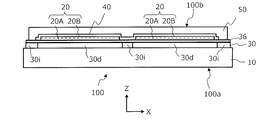
- FIG. 1B is a cross-sectional view of the laminated structure shown in FIG. 1A along the line BB. It is process sectional drawing which shows the manufacturing method of the support substrate in embodiment of this indication. It is process sectional drawing which shows the manufacturing method of the support substrate in embodiment of this indication. It is process sectional drawing which shows the manufacturing method of the support substrate in embodiment of this indication. It is process sectional drawing which shows the manufacturing method of the flexible OLED device in embodiment of this indication. It is process sectional drawing which shows the manufacturing method of the flexible OLED device in embodiment of this indication. It is process sectional drawing which shows the manufacturing method of the flexible OLED device in embodiment of this indication. It is process sectional drawing which shows the manufacturing method of the flexible OLED device in embodiment of this indication. It is process sectional drawing which shows the manufacturing method of the flexible OLED device in embodiment of this indication.
- flexible substrates have been formed from resin materials typified by polyimide. Since such a resin material absorbs ultraviolet rays, it has been considered that the influence of peeling light irradiation on the TFT element and the OLED element does not need to be particularly examined.
- the thickness of the flexible substrate becomes as thin as about 5 ⁇ m to 15 ⁇ m, ultraviolet rays may not be sufficiently absorbed, and the ultraviolet laser light used in the peeling process may be TFT elements and OLED elements. It has been found that there is a possibility of degrading. This problem occurred even when a release layer made of amorphous silicon was provided. This is because amorphous silicon can transmit ultraviolet rays.
- the release layer when the release layer is formed from a refractory metal, the refractory metal absorbs or reflects ultraviolet rays and does not transmit, so that the influence of peeling light irradiation on the TFT element and OLED element can be prevented.
- forming the release layer using a refractory metal causes a significant increase in manufacturing cost.
- the manufacturing method of the flexible OLED device of the present disclosure enables to reduce the influence of the irradiation of the peeling light on the TFT element and the OLED element even when the peeling light can pass through the flexible film.
- FIG. 1A and FIG. 1B Please refer to FIG. 1A and FIG. 1B.
- a laminated structure 100 illustrated in FIGS. 1A and 1B is prepared.
- 1A is a plan view of the laminated structure 100
- FIG. 1B is a cross-sectional view of the laminated structure 100 shown in FIG. 1A along the line BB.
- 1A and 1B show an XYZ coordinate system having an X axis, a Y axis, and a Z axis orthogonal to each other for reference.
- the laminated structure 100 in the present embodiment includes a base (mother substrate or carrier) 10, a flexible film 30 that is positioned between the base 10 and the functional layer region 20 and supports the functional layer region 20, and the flexible film 30.
- a dielectric multilayer mirror (dielectric reflection film) 36 located between the functional layer region 20 is provided.
- the functional layer region 20 includes a TFT layer 20A and an OLED layer 20B.
- the laminated structure 100 further includes a protective sheet 50 that covers the plurality of functional layer regions 20, and a gas barrier film 40 that covers the entire functional layer region 20 between the plurality of functional layer regions 20 and the protective sheet 50. I have.
- the laminated structure 100 may have other layers not shown such as a buffer layer.
- a typical example of the base 10 is a glass base having rigidity.
- a typical example of the flexible film 30 is a synthetic resin film having flexibility.
- the “flexible film” is simply referred to as “resin film”.
- a structure including the dielectric multilayer film mirror 36, the resin film 30 supporting the dielectric multilayer film mirror 36, and the base 10 supporting the resin film 30 as a whole is a “support substrate” of the flexible OLED device. Called.
- the first surface 100a of the laminated structure 100 is defined by the base 10, and the second surface 100b is defined by the protective sheet 50.
- the base 10 and the protective sheet 50 are members temporarily used during the manufacturing process, and are not elements constituting the final flexible OLED device.
- the illustrated resin film 30 includes a plurality of flexible substrate regions 30d that respectively support the plurality of functional layer regions 20, and an intermediate region 30i that surrounds each flexible substrate region 30d.
- the flexible substrate region 30d and the intermediate region 30i are merely different portions of one continuous resin film 30, and need not be physically distinguished.
- the portion of the resin film 30 that is located directly below each functional layer region 20 is the flexible substrate region 30d, and the other portion is the intermediate region 30i.
- Each of the plurality of functional layer regions 20 finally constitutes a panel of a flexible OLED device.
- the laminated structure 100 has a structure in which one base 10 supports a plurality of flexible OLED devices before division.
- Each functional layer region 20 has a shape with a thickness (Z-axis direction size) of several tens of ⁇ m, a length (X-axis direction size) of about 12 cm, and a width (Y-axis direction size) of about 7 cm. is doing. These sizes can be set to any size according to the size of the required display screen.
- the shape of each functional layer region 20 in the XY plane is a rectangle in the illustrated example, but is not limited thereto.
- the shape in the XY plane of each functional layer region 20 may be a square, a polygon, or a shape including a curve in the outline.
- the flexible substrate regions 30d are two-dimensionally arranged in rows and columns corresponding to the arrangement of the flexible OLED devices.
- the intermediate region 30i is composed of a plurality of orthogonal stripes and forms a lattice pattern.
- the width of the stripe is, for example, about 1 to 4 mm.
- the flexible substrate region 30d of the resin film 30 functions as a “flexible substrate” of each flexible OLED device in the form of the final product.
- the intermediate region 30i of the resin film 30 is not an element constituting the final product.
- the configuration of the laminated structure 100 is not limited to the illustrated example.
- the number of functional layer regions 20 supported by one base 10 (the number of OLED devices) is not necessarily plural, and may be single.
- the intermediate region 30 i of the resin film 30 forms a simple frame pattern surrounding the one functional layer region 20.
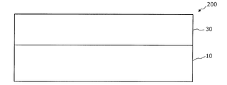
- FIGS. 2A and 2B are process cross-sectional views illustrating a method for manufacturing the support substrate 200 according to an embodiment of the present disclosure.
- a base 10 is prepared.
- the base 10 is a carrier substrate for processing, and the thickness can be, for example, about 0.3 to 0.7 mm.
- the base 10 is typically formed from glass.
- the base 10 is required to transmit peeling light irradiated in a later process.
- the resin film 30 in the present embodiment is a polyimide film having a thickness of 5 ⁇ m to 20 ⁇ m, for example, about 10 ⁇ m.
- the polyimide film can be formed from a precursor polyamic acid or a polyimide solution. Thermal imidization may be performed after the polyamic acid film is formed on the surface of the support substrate 200, or the film may be formed on the surface of the base 10 from a polyimide solution in which polyimide is melted or dissolved in an organic solvent.
- the polyimide solution can be obtained by dissolving a known polyimide in an arbitrary organic solvent.
- a polyimide film can be formed by applying a polyimide solution to the surface of the base 10 and then drying.
- the polyimide film preferably realizes a high transmittance in the entire visible light region.
- the transparency of the polyimide film can be expressed by, for example, the total light transmittance according to JIS K7105-1981.
- the total light transmittance can be set to 80% or more, or 85% or more.
- the top emission type flexible display is not affected by the transmittance.
- the refractive index of the polyimide film is, for example, about 1.7.
- the resin film 30 may be a film formed of a synthetic resin other than polyimide.
- a heat treatment at 350 ° C. or higher is performed in the step of forming the thin film transistor. Therefore, the resin film 30 is formed from a material that does not deteriorate by this heat treatment.
- the resin film 30 may be a laminate of a plurality of synthetic resin films.
- a peeling light irradiation process is performed in which the resin film 30 is irradiated with ultraviolet laser light (wavelength: 300 to 360 nm) that is transmitted through the base 10.
- a release layer such as an amorphous silicon layer that absorbs ultraviolet laser light and releases hydrogen gas may be disposed between the base 10 and the resin film 30.
- a part (layered portion) of the resin film 30 is vaporized at the interface between the base 10 and the resin film 30 by irradiation with ultraviolet laser light, and the resin film 30 can be peeled from the base 10. If there is a release layer, the effect of suppressing the generation of ash is obtained.
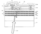
- the dielectric multilayer film mirror 36 described below functions as an ultraviolet transmission suppressing layer in the peeling light irradiation process. As a result, it is avoided or suppressed that ultraviolet laser light enters the functional layer region 20 from the base 10 and deteriorates the characteristics of the TFT layer 20A and the OLED layer 20B.
- the resin film 30 having high transparency absorbs most of ultraviolet rays.
- the resin film 30 used in the flexible OLED device is a very thin layer, the ultraviolet laser light can be incident on the functional layer region 20 in the peeling light irradiation process.
- the ultraviolet laser light may deteriorate not only the characteristics of the TFT layer 20A and the OLED layer 20B but also the sealing performance of the organic film and the inorganic film constituting the sealing structure.
- the resin film 30 that is currently widely used is formed of a yellow-brown or brown-brown polyimide material, it is not recognized that the transmission of ultraviolet laser light can cause deterioration of the characteristics of the functional layer region.
- the method according to the embodiment of the present disclosure is not limited to an OLED device including a resin film (flexible substrate) formed from a material that is highly transparent and easily transmits ultraviolet rays, but also has a low transparency and a thin resin film 30 (thickness). Is suitably used for manufacturing an OLED device having a thickness of about 5 to 20 ⁇ m.
- the target When a polishing target (target) such as a particle or a convex portion exists on the surface of the resin film 30, the target may be polished and flattened by a polishing apparatus. Detection of foreign matters such as particles can be performed by processing an image acquired by an image sensor, for example. After the polishing process, a planarization process may be performed on the surface of the resin film 30.
- the flattening treatment includes a step of forming a film (flattening film) for improving flatness on the surface of the resin film 30.
- the planarizing film need not be made of resin.
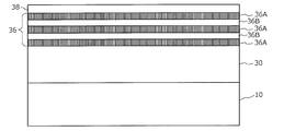
- a dielectric multilayer mirror 36 is formed on the resin film 30.
- the “dielectric multilayer mirror” is a multi-layer stack composed of k dielectric layers, where k is an integer of 5 or more, It means a laminate in which the optical thickness of each dielectric layer is adjusted so that the reflected light from the interface of the dielectric layers having different refractive indexes causes constructive interference.
- the dielectric layer constituting the dielectric multilayer mirror is counted from the side where the peeling light is incident, and the i-th layer is referred to as a dielectric layer (i).
- i is an integer of 1 to k.
- the refractive index of the dielectric layer (i) is n (i) and the thickness is d (i).
- n (i + 1) is lower than n (i) and n (i + 2). Therefore, the odd-numbered dielectric layer (odd number) is referred to as a “high refractive index layer”, and the even-numbered dielectric layer (even number) is referred to as a “low refractive index layer”.
- the optical thickness of the dielectric layer (i) is defined by n (i) ⁇ d (i).
- the thickness of each “high refractive index layer” is the same.
- the “low refractive index layer” is also formed from the same material having the same refractive index, and thus the thickness of each “low refractive index layer” is the same.
- the embodiment of the present disclosure is not limited to such an example.
- the dielectric multilayer mirror 36 includes five dielectric layers (1), a dielectric layer (2), a dielectric layer (3), a dielectric layer (4), and a dielectric layer. (5).
- the dielectric layer (1), the dielectric layer (3), and the dielectric layer (5) are the high refractive index layer 36A.
- the dielectric layer (2) and the dielectric layer (4) are the low refractive index layer 36B.
- the dielectric multilayer film mirror 36 in the example of the figure includes three or more high refractive index layers 36A each having a first refractive index, and a second refractive index lower than the first refractive index.
- low refractive index layers 36B located between the three or more high refractive index layers 36A.
- “high” and “low” in the terms “high refractive index layer” and “low refractive index layer” are not absolute sizes, but are between adjacent dielectric layers so as to form an interface. It means only the relative relationship of refractive index.
- the high refractive index layer is, for example, Si 3 N 4 , SiN x , Al 2 O 3 , HfO 2 , Sc 2 O 3 , Y 2 O 3 , ZrO 2 , Ta 2 O 5 , TiO 2 , and Nb 2 O 5. May be formed from at least one material selected from the group consisting of:
- the low refractive index layer may be formed of at least one material selected from the group consisting of SiO 2 , MgF 2 , CaF 2 , AlF 3 , YF 3 , LiF, and NaF, for example.
- the “high refractive index layer” included in one dielectric multilayer mirror 36 may be formed of a plurality of types of materials having different refractive indexes. In that sense, the “first refractive index” is not limited to singular.
- the terms “low refractive index layer” and “second refractive index” can be similarly interpreted.
- the reflectance at the interface between the high refractive index layer and the low refractive index layer increases as the difference in refractive index between the high refractive index layer and the low refractive index layer increases. For this reason, it is preferable that the material is selected so that the refractive index difference becomes large.
- the low refractive index layer is preferably formed from, for example, a fluorine-based material, and the refractive index is desirably less than 1.5.
- the high refractive index layer is preferably formed from an oxide of a metal such as silicon nitride, tantalum (Ta), hafnium (Hf), yttrium (Y), or niobium (Nb). It is desirable that it is 7 or more.
- the refractive index of the resin film 30 varies depending on the material of the synthetic resin.
- the refractive index of the synthetic resin is typically in the range of about 1.5 to 1.7. For this reason, when the dielectric multilayer mirror 36 is in direct contact with the resin material of the resin film 30, the high refractive index layer 36A included in the dielectric multilayer mirror 36 is disposed so as to be in contact with the resin material. With such an arrangement, the reflectance at the interface between the resin film 30 and the high refractive index layer 36A can be increased.
- a part of the peeling light is first a high refractive index layer which is a dielectric layer (1). Reflected by the interface between 36A and the resin film 30. The light transmitted through this interface is then the interface between the dielectric layer (1) and the dielectric layer (2), the interface between the dielectric layer (2) and the dielectric layer (3), and the dielectric layer (3) and the dielectric. Reflection and transmission are repeated at the interface of the body layer (4) and at the interface of the dielectric layer (4) and the dielectric layer (5), respectively.
- the optical thickness does not need to exactly match the value of ⁇ / 4, and a deviation of ⁇ 20% or less can be allowed.
- the optical thickness when the reflected light from each interface realizes constructive interference may be generally ⁇ / 4 + (L ⁇ ⁇ / 2).
- L is an integer of 0 or more.
- the repetition of the high refractive index layer 36A and the low refractive index layer 36B is 2.5 periods. Embodiments of the present disclosure are not limited to this example.
- the repetition period of the high refractive index layer 36A and the low refractive index layer 36B may be two periods or three periods or more.
- the reflectance was obtained by simulation. The result of this simulation will be described later.
- the dielectric multilayer mirror 36 is produced by alternately forming the high refractive index layer 36A and the low refractive index layer 36B by a thin film deposition technique such as vapor deposition.
- the high refractive index layer 36A and the low refractive index layer 36B are typically continuous films, but may be patterned.
- the dielectric multilayer mirror 36 only needs to be present in a region where the peeling light is prevented from entering the TFT layer 20A and the OLED layer 20B.
- the dielectric multilayer mirror 36 may be formed on the resin film 30 before pasting.
- the dielectric multilayer mirror 36 is a member that exhibits an optical function when irradiated with peeling light in the lift-off process.
- ultraviolet rays contained in ambient light are applied to the TFT layer 20A and the OLED layer. It can also exhibit a function of suppressing the deterioration with aging upon entering into 20B.
- the dielectric multilayer mirror 36 not only exhibits an optical function, but can also exhibit a gas barrier film function described below.
- a gas barrier film 38 is formed on the dielectric multilayer mirror 36 as shown in FIG. 3A.
- the gas barrier film 38 can have various structures.
- An example of the gas barrier film is a film such as a silicon oxide film or a silicon nitride film.
- Another example of the gas barrier film may be a multilayer film in which an organic material layer and an inorganic material layer are stacked. This gas barrier film may be referred to as a “lower gas barrier film” in order to distinguish it from a gas barrier film described later that covers the functional layer region 20. Further, the gas barrier film covering the functional layer region 20 can be referred to as an “upper gas barrier film”.
- the gas barrier film 38 may be in contact with the high refractive index layer 36A or the low refractive index layer 36B constituting the dielectric multilayer mirror 36, or between the gas barrier film 38 and the dielectric multilayer mirror 36. Other layers may intervene.
- the gas barrier film 38 and the dielectric multilayer mirror 36 are in direct contact with each other, it is preferable that the peeling light is strongly reflected also by the interface between the gas barrier film 38 and the dielectric multilayer mirror 36.
- the dielectric layer in contact with the gas barrier film 38 is desirably formed of a material having a refractive index substantially different from the refractive index of the gas barrier film 38.
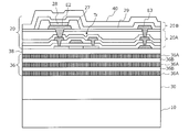
- the functional layer region 20 includes a TFT layer 20A located in the lower layer and an OLED layer 20B located in the upper layer.
- the TFT layer 20A and the OLED layer 20B are sequentially formed by a known method.
- the TFT layer 20A includes a TFT array circuit that realizes an active matrix.
- the OLED layer 20B includes an array of OLED elements, each of which can be driven independently.
- the thickness of the TFT layer 20A is, for example, 4 ⁇ m, and the thickness of the OLED layer 20B is, for example, 1 ⁇ m.
- the semiconductor layer 21 is formed on the lower gas barrier film 38.
- the semiconductor layer is amorphous at this stage.
- the semiconductor layer 21 is irradiated with laser light.
- part of the laser light may pass through the semiconductor layer 21 and enter the dielectric multilayer mirror 36.
- the heat treatment conditions such as the temperature rise rate of the semiconductor layer 21 may change as compared with the case where the dielectric multilayer mirror 36 is not provided. .
- the semiconductor layer 21 is made of silicon
- a large refractive index difference occurs between the lower gas barrier film 38 and the semiconductor layer 21.
- the lower gas barrier film 38 is made of, for example, SiN x (refractive index: about 1.9)
- the refractive index of silicon is 4 or more
- a large refractive index difference occurs at the interface
- Laser light is strongly reflected at this interface.
- the influence of the laser light transmitted through this interface and reflected by the dielectric multilayer mirror 36 is reduced. This means that it is not necessary to change the laser light irradiation conditions for polycrystallizing the semiconductor layer 21 depending on the presence or absence of the dielectric reflecting mirror.
- the reflectivity of the dielectric multilayer mirror 36 is optimized according to the wavelength of the peeling light. For this reason, since such a dielectric multilayer mirror 36 does not strongly reflect light of other wavelengths, fluctuations in semiconductor polycrystallization conditions are unlikely to occur in the first place.
- a TFT layer 20A is formed by a known TFT manufacturing process. Specifically, after patterning the semiconductor layer 21, the ground line GL is formed. After forming the gate insulating film 22, the gate electrode G is formed so as to cover the channel region of the semiconductor layer 21. Source / drain regions self-aligned with the gate electrode G are formed in the semiconductor layer 21 by ion implantation. After the interlayer insulating film 23 is deposited, contact holes are formed, and the source electrode S and drain electrode D of the transistor Tr and the electrode E1 on the ground line GL are formed. After depositing the first inorganic barrier layer 24 covering these, an organic planarizing film 25 and a second inorganic barrier layer 26 are formed. Thus, the TFT layer 20A is formed.
- the configuration and manufacturing method of the TFT layer 20A are not limited to this example, and may be various.
- the anode electrode E2 and the cathode electrode E3 of the OLED light emitting element 28 are formed.
- the bank 27 is formed, the OLED light emitting element 28 is formed on the anode electrode E2.
- the OLED light emitting element 28 includes organic semiconductor layers such as a hole transport layer, a light emitting layer, and an electron transport layer.
- the OLED layer 20B is formed by forming the transparent electrode 29 that electrically connects the electron transport layer of the OLED light-emitting element 28 and the cathode electrode E3.
- the configuration and manufacturing method of the OLED layer 20B are not limited to this example, and may vary. Thus, the functional layer region 20 is completed.
- a thin film sealing layer (upper gas barrier film) 40 As shown in FIG. 3D.
- a typical example of the upper gas barrier film 40 is a multilayer film in which an inorganic material layer and an organic material layer are laminated. Elements such as an adhesive film, another functional layer constituting a touch screen, and a polarizing film may be disposed between the upper gas barrier film 40 and the functional layer region 20 or further above the upper gas barrier film 40.
- the upper gas barrier film 40 can be formed by a thin film encapsulation (TFE) technique.
- the WVTR Water Vapor Transmission Rate
- the WVTR Water Vapor Transmission Rate of the thin film sealing structure is typically required to be 1 ⁇ 10 ⁇ 4 g / m 2 / day or less. This criterion is achieved according to embodiments of the present disclosure.
- the thickness of the upper gas barrier film 40 is, for example, 1.5 ⁇ m or less.
- the protective sheet 50 (FIG. 1B) is attached to the upper surface of the laminated structure 100.
- the protective sheet 50 can be formed of a material such as polyethylene terephthalate (PET) or polyvinyl chloride (PVC).
- PET polyethylene terephthalate
- PVC polyvinyl chloride
- a typical example of the protective sheet 50 has a laminated structure having a release agent coating layer on the surface.
- the thickness of the protective sheet 50 can be, for example, 50 ⁇ m or more and 150 ⁇ m or less.
- the manufacturing method according to the present disclosure can be performed using a manufacturing apparatus (peeling apparatus 220) described later.
- the laminated structure 100 that can be used in the manufacturing method of the present disclosure is not limited to the example shown in FIGS. 1A and 1B.
- the protective sheet 50 may cover the entirety of the resin film 30 and may extend outward from the resin film 30.
- the protective sheet 50 may cover the entirety of the resin film 30 and extend outward from the base 10.
- the laminated structure 100 becomes a flexible thin sheet-like structure having no rigidity.
- the protective sheet 50 impacts the functional layer region 20 when the functional layer region 20 collides with or comes into contact with an external device or instrument in the step of peeling the base 10 and the step after peeling. It plays a role to protect against friction.
- a typical example of the protective sheet 50 has a laminate structure having an adhesive layer (application layer of a release agent) having a relatively low adhesive force on the surface. is doing. A more detailed description of the laminated structure 100 will be described later.
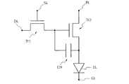
- FIG. 4 is a basic equivalent circuit diagram of sub-pixels in an organic EL (Electro Luminescence) display.
- One pixel of the display can be composed of sub-pixels of different colors such as R (red), G (green), and B (blue).
- the example shown in FIG. 4 includes a selection TFT element Tr1, a driving TFT element Tr2, a storage capacitor CH, and an OLED element EL.
- the selection TFT element Tr1 is connected to the data line DL and the selection line SL.
- the data line DL is a wiring that carries a data signal that defines an image to be displayed.
- the data line DL is electrically connected to the gate of the driving TFT element Tr2 via the selection TFT element Tr1.
- the selection line SL is a wiring that carries a signal for controlling on / off of the selection TFT element Tr1.
- the driving TFT element Tr2 controls a conduction state between the power line PL and the OLED element EL. When the driving TFT element Tr2 is turned on, a current flows from the power line PL to the ground line GL via the OLED element EL. This current causes the OLED element EL to emit light. Even if the selection TFT element Tr1 is turned off, the ON state of the driving TFT element Tr2 is maintained by the storage capacitor CH.
- the driving TFT element Tr2 corresponds to the transistor Tr in FIG. 3D.
- the TFT layer 20A includes a selection TFT element Tr1, a driving TFT element Tr2, a data line DL, a selection line SL, and the like.
- the OLED layer 20B includes an OLED element EL. Before the OLED layer 20B is formed, the upper surface of the TFT layer 20A is flattened by an interlayer insulating film that covers the TFT array and various wirings. A structure that supports the OLED layer 20B and realizes active matrix driving of the OLED layer 20B is referred to as a “backplane”.
- TFT layer 20A may be included in either the TFT layer 20A or the OLED layer 20B. 4 is connected to a driver circuit (not shown).
- the specific configurations of the TFT layer 20A and the OLED layer 20B may vary. These configurations do not limit the content of the present disclosure.
- the configuration of the TFT element included in the TFT layer 20A may be a bottom gate type or a top gate type.
- the light emission of the OLED element included in the OLED layer 20B may be a bottom emission type or a top emission type.
- the specific configuration of the OLED element is also arbitrary.
- the material of the semiconductor layer constituting the TFT element includes, for example, crystalline silicon, amorphous silicon, and an oxide semiconductor.
- a part of the process of forming the TFT layer 20A includes a heat treatment process at 350 ° C. or higher in order to improve the performance of the TFT element.
- FIG. 5 is a perspective view schematically showing the upper surface side of the laminated structure 100 at the stage where the upper gas barrier film 40 is formed.
- One laminated structure 100 includes a plurality of OLED devices 1000 supported by the base 10.
- one laminated structure 100 includes more functional layer regions 20 than the example shown in FIG. 1A. As described above, the number of functional layer regions 20 supported by one base 10 is arbitrary.
- the step of dividing the intermediate region 30i of the resin film 30 and each of the plurality of flexible substrate regions 30d is performed.
- the process of dividing does not need to be performed before the LLO process, and may be performed after the LLO process.
- the division can be performed by cutting the central portion of the adjacent OLED device with a laser beam or a dicing saw.
- parts other than the base 10 of a laminated structure are cut
- the base 10 may be cut and divided into partial laminated structures including individual OLED devices and a base portion that supports each OLED device.
- the irradiation position of the laser beam for cutting is along the outer periphery of each flexible substrate region 30d.
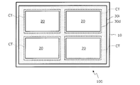
- 6A and 6B are a cross-sectional view and a plan view schematically showing positions where the intermediate region 30i of the resin film 30 and each of the plurality of flexible substrate regions 30d are divided.
- the irradiation position of the laser beam for cutting is along the outer periphery of each flexible substrate region 30d.
- an irradiation position (cutting position) CT indicated by an arrow or a broken line is irradiated with a cutting laser beam, and a portion other than the base 10 in the laminated structure 100 is provided with a plurality of OLED devices 1000 and others. Cut into unnecessary parts.
- gaps of several tens to several hundreds of ⁇ m are formed between the individual OLED devices 1000 and the periphery thereof. As described above, such cutting can be performed by a dicing saw instead of the laser beam irradiation. Even after the cutting, the OLED device 1000 and other unnecessary portions are fixed to the base 10.
- the planar layout of “unnecessary portions” in the laminated structure 100 matches the planar layout of the intermediate region 30 i of the resin film 30.
- this “unnecessary portion” is a continuous sheet-like structure having an opening.
- the irradiation position CT of the cutting laser beam may be set so that the “unnecessary portion” is divided into a plurality of portions.
- the sheet-like structure that is an “unnecessary portion” includes not only the intermediate region 30 i of the resin film 30 but also the cut portions of the laminate (eg, the gas barrier film 40 and the protective sheet 50) existing on the intermediate region 30 i. Contains.
- the wavelength of the laser beam may be in any region of infrared, visible light, and ultraviolet. From the viewpoint of reducing the influence of cutting on the base 10, a laser beam whose wavelength is included in the green to ultraviolet region is desirable.
- cutting can be performed using the second harmonic (wavelength 532 nm) or the third harmonic (wavelength 343 nm or 355 nm). In that case, if the laser output is adjusted to 1 to 3 watts and scanned at a speed of about 500 mm per second, the laminate supported by the base 10 can be used as an OLED device and an unnecessary part without damaging the base 10. Can be cut (divided).
- the timing for performing the above-described cutting is earlier than in the related art. Since the cutting is performed in a state where the resin film 30 is fixed to the base 10, even when the interval between the adjacent OLED devices 1000 is narrow, the cutting position can be aligned with high accuracy and precision. For this reason, the space
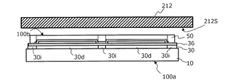
- FIG. 7A is a diagram schematically showing a state immediately before the stage 212 supports the laminated structure 100 in a manufacturing apparatus (peeling apparatus) (not shown).
- the stage 212 in the present embodiment is an adsorption stage having a large number of holes for adsorption on the surface.
- the configuration of the suction stage is not limited to this example, and may include an electrostatic chuck or other fixing device that supports the laminated structure.
- the laminated structure 100 is disposed such that the second surface 100b of the laminated structure 100 faces the surface 212S of the stage 212, and is in close contact with the stage 212.
- FIG. 7B is a diagram schematically showing a state in which the stage 212 supports the laminated structure 100.
- the arrangement relationship between the stage 212 and the laminated structure 100 is not limited to the illustrated example.
- the stacked structure 100 may be turned upside down and the stage 212 may be positioned below the stacked structure 100.
- the laminated structure 100 is in contact with the surface 212S of the stage 212, and the stage 212 adsorbs the laminated structure 100.
- FIG. 7C is a diagram schematically showing a state in which the resin film 30 is irradiated from the base 10 side by the peeling light 216 formed in a line shape extending in a direction perpendicular to the drawing sheet.
- the resin film 30 absorbs ultraviolet laser light and is heated in a short time. A part of the resin film 30 is vaporized or decomposed (disappeared) at the interface between the base 10 and the resin film 30.
- the wavelength of the peeling light 216 is in the ultraviolet region.
- the light absorption rate of the base 10 is, for example, about 10% in the wavelength region of 343 to 355 nm, but can increase to 30 to 60% at 308 nm.
- FIG. 7D schematically shows a state in which the peeling light 216 is incident on the resin film 30.
- the peeling light 216 is incident on the resin film 30 obliquely.
- the peeling light 216 typically enters the resin film 30 perpendicularly.
- FIG. 7D schematically shows a state where a part of the peeling light 216 transmitted through the resin film 30 is reflected from the dielectric multilayer mirror 36.
- the repetition of the high refractive index layer and the low refractive index layer is 2.5 periods, but the reflectance increases as the number of periods increases.
- the reflectance increases as the number of periods increases.
- the reflectivity should be 30% or more, and if it is 50% or more, a sufficient effect can be obtained.
- the semiconductor layer 21 is irradiated with laser light to improve the crystallinity of the semiconductor layer 21.
- This laser light enters the semiconductor layer 21 from the direction shown in FIG. 3B.
- the peeling light 216 passes through the base 10 and the resin film 30 and then enters the dielectric multilayer mirror 36.
- the laser light for polycrystallizing the semiconductor layer 21 is a semiconductor light. After passing through the layer 21, the light enters the dielectric multilayer mirror 36.
- the wavelength of the laser beam for modifying the semiconductor does not need to match the wavelength of the peeling light, and can be selected from a band suitable for polycrystallizing the semiconductor layer 21.
- a laser irradiation apparatus for polycrystallizing a semiconductor layer such as silicon an excimer laser apparatus that emits laser light having a wavelength of 308 nm is widely used.
- the presence of the dielectric multilayer mirror 36 effectively realizes the reflection of the peeling light.
- we studied to reduce the influence on the modification of the semiconductor layer This is because if the degree of modification of the semiconductor layer 21 is uneven, the characteristics of the TFT that drives the sub-pixel of the organic EL display will be different for each TFT.
- the variation in TFT characteristics causes luminance unevenness for each pixel in an organic EL display that operates by current drive, and degrades display quality.
- a gas barrier film 38 formed of an inorganic material is disposed between the semiconductor layer 21 and the dielectric multilayer mirror 36, and the thickness of the gas barrier film 38 is adjusted to an appropriate size.
- Table 5, Table 6, Table 7 and Table 8 show that the wavelength of the laser beam used for polycrystallization of the semiconductor layer is maintained at a relatively high reflectance at the wavelength (346 nm or 355 nm) of the laser beam used for peeling. (308 nm) shows an example of a configuration in which the reflectance is relatively lowered.
- the reflectances at wavelengths of 343 nm and 355 nm are set to 76.4% and 85.7%, respectively.
- the reflectance at a wavelength of 308 nm is 12.4%.
- reflectances at wavelengths of 343 nm and 355 nm are 60.9% and 63.6%, respectively.
- the reflectances at wavelengths of 343 nm and 355 nm are 60.8% and 78.0%, respectively.
- the reflectances at wavelengths of 343 nm and 355 nm are set to 53.8% and 71.5%, respectively.
- the reflectance of the dielectric multilayer mirror 36 can be made more semiconductor than the wavelength of the peeling light (first wavelength).
- the wavelength of the laser beam for layer modification (second wavelength) can be relatively lowered.
- the high refractive index layer included in the dielectric multilayer mirror 36 is generally made of a dense material and exhibits a barrier effect against a gas such as water vapor. For this reason, it can be expected that the moisture resistance of the flexible OLED device is improved when the total thickness of the high refractive index layers included in the dielectric multilayer mirror 36 is 100 nm or more. Since the dielectric multilayer film mirror 36 can also exhibit a function of improving moisture resistance in addition to the optical function, when the gas barrier film 38 is disposed between the dielectric multilayer film mirror 36 and the functional layer region 20, the gas barrier film The thickness of 38 can also be 200 nm or less.
- the peeling apparatus includes a line beam light source that emits the peeling light 216.
- the line beam light source includes a laser device and an optical system that shapes laser light emitted from the laser device into a line beam shape.
- FIG. 8A is a perspective view schematically showing a state in which the laminated structure 100 is irradiated with a line beam (peeling light 216) emitted from the line beam light source 214 of the peeling device 220.
- FIG. 8A For the sake of clarity, the stage 212, the stacked structure 100, and the line beam light source 214 are illustrated as being separated in the Z-axis direction of the drawing.
- the peeling light 216 is irradiated, the second surface 100 b of the stacked structure 100 is in contact with the stage 212.
- FIG. 8B schematically shows the position of the stage 212 when the peeling light 216 is irradiated. Although not shown in FIG. 8B, the laminated structure 100 is supported by the stage 212.
- Examples of a laser device that emits the peeling light 216 include a gas laser device such as an excimer laser, a solid-state laser device such as a YAG laser, a semiconductor laser device, and other laser devices. According to the XeCl excimer laser device, laser light having a wavelength of 308 nm can be obtained.
- neodymium (Nd) is doped yttrium vanadium tetraoxide (YVO 4), or ytterbium (Yb) uses YVO 4 doped as lasing medium, a laser beam (fundamental emitted from the laser gain medium Therefore, it can be used after being converted into laser light (third harmonic) having a wavelength of 340 to 360 nm by the wavelength conversion element.
- YVO 4 yttrium vanadium tetraoxide
- Yb ytterbium
- Irradiation of the peeling light 216 can be performed with an energy irradiation density of, for example, 50 to 400 mJ / cm 2 .
- the line beam-like peeling light 216 has a size that traverses the base 10, that is, a line length (long axis dimension, Y axis direction size in FIG. 8B) that exceeds the length of one side of the base.
- the line length can be, for example, 750 mm or more.
- the line width (short axis dimension, X-axis direction size in FIG. 8B) of the peeling light 216 may be about 0.2 mm, for example. These dimensions are the size of the irradiation region at the interface between the resin film 30 and the base 10.
- the peeling light 216 can be irradiated as a pulse or continuous wave. Pulsed irradiation can be performed at a frequency of about 200 times per second, for example.
- the irradiation position of the peeling light 216 moves relative to the base 10, and the scanning of the peeling light 216 is executed.
- a light source 214 that emits peeling light and an optical device may be fixed, and the laminated structure 100 may move, or vice versa.
- irradiation of the peeling light 216 is performed while the stage 212 moves from the position shown in FIG. 8B to the position shown in FIG. 8C. That is, the scanning of the peeling light 216 is executed by the movement of the stage 212 along the X-axis direction.
- FIG. 9A describes a state in which the laminated structure 100 is in contact with the stage 212 after irradiation with peeling light. While maintaining this state, the distance from the stage 212 to the base 10 is increased. At this time, the stage 212 in this embodiment sucks the OLED device portion of the laminated structure 100.
- a drive device holds the base 10 and moves the entire base 10 in the direction of the arrow, thereby performing peeling (lift-off).
- the base 10 can move together with the suction stage while being sucked by a suction stage (not shown).
- the direction of movement of the base 10 does not need to be perpendicular to the first surface 100a of the laminated structure 100, and may be inclined.
- the movement of the base 10 does not have to be a linear motion, and may be a rotational motion.
- the base 10 may be fixed by a holding device (not shown) or another stage, and the stage 212 may move upward in the drawing.
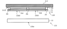
- FIG. 9B is a cross-sectional view showing the first portion 110 and the second portion 120 of the laminated structure 100 thus separated.
- the first portion 110 of the stacked structure 100 includes a plurality of OLED devices 1000 in contact with the stage 212.
- Each OLED device 1000 has a functional layer region 20 and a plurality of flexible substrate regions 30 d of the resin film 30.
- the second portion 120 of the laminated structure 100 is the base 10.
- the individual OLED devices 1000 supported by the stage 212 are in a mutually disconnected relationship, they can be easily detached from the stage 212 simultaneously or sequentially.
- each OLED device 1000 is cut and separated before the LLO process, but each OLED device 1000 may be cut and separated after the LLO process. Also, the cutting and separation of each OLED device 1000 may include dividing the base 10 into corresponding portions.
- FIG. 10 is a cross-sectional view showing a flexible OLED device according to an embodiment of the present disclosure.
- the functional layer region 20 is supported by the flexible substrate region 30 d of the resin film 30 peeled from the base 10.
- a flexible film when a flexible film is used from highly transparent polyimide and PET that transmits ultraviolet rays, or a flexible film that is low in transparency but thin (thickness: 5 to 20 ⁇ m) and can transmit ultraviolet rays is used. Even in this case, it is possible to suppress the characteristic deterioration of the functional layer region and the performance deterioration of the gas barrier film due to the ultraviolet rays.
- Embodiments of the present invention provide a method for manufacturing a new flexible OLED device.
- the flexible OLED device can be widely applied to smartphones, tablet terminals, in-vehicle displays, and small to medium-sized television devices.
- SYMBOLS 10 Base, 20 ... Functional layer region, 20A ... TFT layer, 20B ... OLED layer, 30 ... Resin film, 30d ... Flexible substrate region of resin film, 30i ... Intermediate region of resin film, 40 ... gas barrier film, 50 ... protective sheet, 100 ... laminated structure, 212 ... stage, 1000 ... OLED device
Landscapes
- Engineering & Computer Science (AREA)
- Manufacturing & Machinery (AREA)
- Electroluminescent Light Sources (AREA)
Abstract
Selon le procédé de fabrication d'un dispositif DELO souple de la présente invention, une structure stratifiée (100) est préparée, la structure stratifiée (100) étant pourvue : d'une base (10) ; d'une région de couche fonctionnelle (20) comprenant une couche TFT et une couche DELO ; d'un film souple (30) qui est situé entre la base et la région de couche fonctionnelle et qui supporte la région de couche fonctionnelle ; et d'un miroir film multicouche diélectrique (36) qui est situé entre le film souple et la région de couche fonctionnelle. Le film souple est délaminé à partir de la base par exposition du film souple à une lumière de délaminage (216) transmise à travers la base.
Priority Applications (5)
| Application Number | Priority Date | Filing Date | Title |
|---|---|---|---|
| US16/767,466 US10903460B2 (en) | 2018-03-20 | 2018-03-20 | Flexible OLED device, method for manufacturing same, and support substrate |
| CN201880078128.6A CN111869327A (zh) | 2018-03-20 | 2018-03-20 | 柔性oled装置及其制造方法以及支承基板 |
| PCT/JP2018/011074 WO2019180823A1 (fr) | 2018-03-20 | 2018-03-20 | Dispositif delo souple, son procédé de fabrication et substrat de support |
| JP2019564179A JP6666530B2 (ja) | 2018-03-20 | 2018-03-20 | フレキシブルoledデバイス及びその製造方法並びに支持基板 |
| US17/122,896 US20210104709A1 (en) | 2018-03-20 | 2020-12-15 | Flexible oled device, method for manufacturing same, and support substrate |
Applications Claiming Priority (1)
| Application Number | Priority Date | Filing Date | Title |
|---|---|---|---|
| PCT/JP2018/011074 WO2019180823A1 (fr) | 2018-03-20 | 2018-03-20 | Dispositif delo souple, son procédé de fabrication et substrat de support |
Related Child Applications (2)
| Application Number | Title | Priority Date | Filing Date |
|---|---|---|---|
| US16/767,466 A-371-Of-International US10903460B2 (en) | 2018-03-20 | 2018-03-20 | Flexible OLED device, method for manufacturing same, and support substrate |
| US17/122,896 Continuation US20210104709A1 (en) | 2018-03-20 | 2020-12-15 | Flexible oled device, method for manufacturing same, and support substrate |
Publications (1)
| Publication Number | Publication Date |
|---|---|
| WO2019180823A1 true WO2019180823A1 (fr) | 2019-09-26 |
Family
ID=67986064
Family Applications (1)
| Application Number | Title | Priority Date | Filing Date |
|---|---|---|---|
| PCT/JP2018/011074 Ceased WO2019180823A1 (fr) | 2018-03-20 | 2018-03-20 | Dispositif delo souple, son procédé de fabrication et substrat de support |
Country Status (4)
| Country | Link |
|---|---|
| US (2) | US10903460B2 (fr) |
| JP (1) | JP6666530B2 (fr) |
| CN (1) | CN111869327A (fr) |
| WO (1) | WO2019180823A1 (fr) |
Cited By (1)
| Publication number | Priority date | Publication date | Assignee | Title |
|---|---|---|---|---|
| JP2024529241A (ja) * | 2021-06-17 | 2024-08-06 | アプライド マテリアルズ インコーポレイテッド | Led製造プロセス用光吸収バリア |
Families Citing this family (4)
| Publication number | Priority date | Publication date | Assignee | Title |
|---|---|---|---|---|
| CN212392267U (zh) | 2019-09-29 | 2021-01-22 | 京东方科技集团股份有限公司 | 显示基板母板以及显示基板 |
| TWI743722B (zh) * | 2020-03-30 | 2021-10-21 | 元太科技工業股份有限公司 | 顯示裝置 |
| CN112967601A (zh) * | 2021-02-04 | 2021-06-15 | 武汉华星光电半导体显示技术有限公司 | 保护膜、显示面板的制作方法 |
| FR3155625A1 (fr) | 2023-11-20 | 2025-05-23 | Soitec | Support muni d’un miroir de bragg, prevu pour le transfert d’une couche par separation laser |
Citations (8)
| Publication number | Priority date | Publication date | Assignee | Title |
|---|---|---|---|---|
| JP2011076767A (ja) * | 2009-09-29 | 2011-04-14 | Dainippon Printing Co Ltd | 積層体、準備用支持体、積層体の製造方法、及びデバイスの製造方法 |
| WO2013005254A1 (fr) * | 2011-07-06 | 2013-01-10 | パナソニック株式会社 | Procédé de fabrication d'un dispositif flexible, ainsi que dispositif flexible |
| CN203503661U (zh) * | 2013-09-24 | 2014-03-26 | 京东方科技集团股份有限公司 | 柔性显示基板、柔性显示装置 |
| US20150042913A1 (en) * | 2013-08-08 | 2015-02-12 | Samsung Display Co., Ltd. | Flexible display having damage impeding layer and method for manufacturing the same |
| US20150380439A1 (en) * | 2013-09-25 | 2015-12-31 | Boe Technology Group Co., Ltd. | Flexible display substrate and manufacturing method thereof, and flexible display device |
| US20160197293A1 (en) * | 2013-09-24 | 2016-07-07 | Boe Technology Group Co., Ltd. | Flexible display substrate and manufacturing method thereof, and flexible display device |
| JP2016134307A (ja) * | 2015-01-20 | 2016-07-25 | 富士フイルム株式会社 | フレキシブルデバイスの製造方法、および、フレキシブルデバイス積層体 |
| US20170170329A1 (en) * | 2015-12-10 | 2017-06-15 | Industrial Technology Research Institute | Flexible device |
Family Cites Families (6)
| Publication number | Priority date | Publication date | Assignee | Title |
|---|---|---|---|---|
| JP3809681B2 (ja) | 1996-08-27 | 2006-08-16 | セイコーエプソン株式会社 | 剥離方法 |
| JP3318285B2 (ja) | 1999-05-10 | 2002-08-26 | 松下電器産業株式会社 | 薄膜トランジスタの製造方法 |
| JP2005079312A (ja) | 2003-08-29 | 2005-03-24 | Mitsubishi Electric Corp | 半導体装置の製造方法およびそれに用いられる半導体製造装置並びに液晶表示装置 |
| US8168511B2 (en) | 2007-09-20 | 2012-05-01 | Sharp Kabushiki Kaisha | Display device manufacturing method and laminated structure |
| CN102089858B (zh) * | 2008-02-20 | 2013-03-13 | 夏普株式会社 | 柔性半导体基板的制造方法 |
| JP6424456B2 (ja) * | 2013-07-17 | 2018-11-21 | セイコーエプソン株式会社 | 発光装置、発光装置の製造方法、受発光装置、電子機器 |
-
2018
- 2018-03-20 JP JP2019564179A patent/JP6666530B2/ja not_active Expired - Fee Related
- 2018-03-20 US US16/767,466 patent/US10903460B2/en not_active Expired - Fee Related
- 2018-03-20 CN CN201880078128.6A patent/CN111869327A/zh active Pending
- 2018-03-20 WO PCT/JP2018/011074 patent/WO2019180823A1/fr not_active Ceased
-
2020
- 2020-12-15 US US17/122,896 patent/US20210104709A1/en not_active Abandoned
Patent Citations (8)
| Publication number | Priority date | Publication date | Assignee | Title |
|---|---|---|---|---|
| JP2011076767A (ja) * | 2009-09-29 | 2011-04-14 | Dainippon Printing Co Ltd | 積層体、準備用支持体、積層体の製造方法、及びデバイスの製造方法 |
| WO2013005254A1 (fr) * | 2011-07-06 | 2013-01-10 | パナソニック株式会社 | Procédé de fabrication d'un dispositif flexible, ainsi que dispositif flexible |
| US20150042913A1 (en) * | 2013-08-08 | 2015-02-12 | Samsung Display Co., Ltd. | Flexible display having damage impeding layer and method for manufacturing the same |
| CN203503661U (zh) * | 2013-09-24 | 2014-03-26 | 京东方科技集团股份有限公司 | 柔性显示基板、柔性显示装置 |
| US20160197293A1 (en) * | 2013-09-24 | 2016-07-07 | Boe Technology Group Co., Ltd. | Flexible display substrate and manufacturing method thereof, and flexible display device |
| US20150380439A1 (en) * | 2013-09-25 | 2015-12-31 | Boe Technology Group Co., Ltd. | Flexible display substrate and manufacturing method thereof, and flexible display device |
| JP2016134307A (ja) * | 2015-01-20 | 2016-07-25 | 富士フイルム株式会社 | フレキシブルデバイスの製造方法、および、フレキシブルデバイス積層体 |
| US20170170329A1 (en) * | 2015-12-10 | 2017-06-15 | Industrial Technology Research Institute | Flexible device |
Cited By (2)
| Publication number | Priority date | Publication date | Assignee | Title |
|---|---|---|---|---|
| JP2024529241A (ja) * | 2021-06-17 | 2024-08-06 | アプライド マテリアルズ インコーポレイテッド | Led製造プロセス用光吸収バリア |
| JP7728370B2 (ja) | 2021-06-17 | 2025-08-22 | アプライド マテリアルズ インコーポレイテッド | Led製造プロセス用光吸収バリア |
Also Published As
| Publication number | Publication date |
|---|---|
| US10903460B2 (en) | 2021-01-26 |
| US20200381674A1 (en) | 2020-12-03 |
| US20210104709A1 (en) | 2021-04-08 |
| JPWO2019180823A1 (ja) | 2020-04-23 |
| JP6666530B2 (ja) | 2020-03-13 |
| CN111869327A (zh) | 2020-10-30 |
Similar Documents
| Publication | Publication Date | Title |
|---|---|---|
| JP6666530B2 (ja) | フレキシブルoledデバイス及びその製造方法並びに支持基板 | |
| CN100595931C (zh) | 电致发光显示装置和用于电致发光显示装置的热转移给体膜 | |
| US9472650B2 (en) | Manufacturing method of flexible display device | |
| EP2804231A2 (fr) | Affichage à diode électroluminescente organique, dispositif électronique comprenant celui-ci et procédé de fabrication dudit dispositif d'affichage | |
| CN103500745A (zh) | 柔性显示基板及其制备方法、柔性显示装置 | |
| US10026930B2 (en) | Method of manufacturing display apparatus | |
| WO2019082357A1 (fr) | Procédé et dispositif de fabrication d'un dispositif delo flexible | |
| KR20190136142A (ko) | 표시 장치, 그 제조 방법 및 표시 장치 제조를 위한 레이저 가공 장치 | |
| JP6588186B1 (ja) | フレキシブルoledデバイスの製造方法及び支持基板 | |
| CN112670320B (zh) | 显示设备和用于制造显示设备的设备 | |
| TW201423978A (zh) | 顯示裝置及其製造方法 | |
| JP6851519B2 (ja) | フレキシブルoledデバイス及びその製造方法並びに支持基板 | |
| JP6564555B1 (ja) | フレキシブルoledデバイス、その製造方法及び支持基板 | |
| CN203503658U (zh) | 柔性显示基板及柔性显示装置 | |
| JP6899477B2 (ja) | フレキシブルoledデバイス、その製造方法及び支持基板 | |
| KR20100136728A (ko) | 다중 전사 가능한 전사기판 및 이를 이용하는 전사방법 | |
| TWI843221B (zh) | 用於無偏光器led顯示器的發光像素和子像素結構及形成發光像素的處理方法 | |
| US20100282724A1 (en) | Laser irradiation apparatus and method of manufacturing display device using the same | |
| JP6772348B2 (ja) | フレキシブルoledデバイス、その製造方法及び支持基板 | |
| KR20160027429A (ko) | 유기발광표시장치의 제조방법 | |
| WO2021005798A1 (fr) | Procédé de fabrication de dispositif électroluminescent souple et substrat de support | |
| JP2008147016A (ja) | 蒸着薄膜のパターン形成方法およびそれを用いた有機elパネルの製造方法 | |
| WO2021005796A1 (fr) | Dispositif électroluminescent souple, son procédé de fabrication et substrat de support |
Legal Events
| Date | Code | Title | Description |
|---|---|---|---|
| 121 | Ep: the epo has been informed by wipo that ep was designated in this application |
Ref document number: 18910618 Country of ref document: EP Kind code of ref document: A1 |
|
| ENP | Entry into the national phase |
Ref document number: 2019564179 Country of ref document: JP Kind code of ref document: A |
|
| NENP | Non-entry into the national phase |
Ref country code: DE |
|
| 122 | Ep: pct application non-entry in european phase |
Ref document number: 18910618 Country of ref document: EP Kind code of ref document: A1 |