WO2019181740A1 - Outil de coupe revêtu en surface - Google Patents
Outil de coupe revêtu en surface Download PDFInfo
- Publication number
- WO2019181740A1 WO2019181740A1 PCT/JP2019/010612 JP2019010612W WO2019181740A1 WO 2019181740 A1 WO2019181740 A1 WO 2019181740A1 JP 2019010612 W JP2019010612 W JP 2019010612W WO 2019181740 A1 WO2019181740 A1 WO 2019181740A1
- Authority
- WO
- WIPO (PCT)
- Prior art keywords
- layer
- cutting tool
- group
- coated cutting
- elements
- Prior art date
- Legal status (The legal status is an assumption and is not a legal conclusion. Google has not performed a legal analysis and makes no representation as to the accuracy of the status listed.)
- Ceased
Links
Images



Classifications
-
- B—PERFORMING OPERATIONS; TRANSPORTING
- B23—MACHINE TOOLS; METAL-WORKING NOT OTHERWISE PROVIDED FOR
- B23B—TURNING; BORING
- B23B27/00—Tools for turning or boring machines; Tools of a similar kind in general; Accessories therefor
- B23B27/14—Cutting tools of which the bits or tips or cutting inserts are of special material
- B23B27/148—Composition of the cutting inserts
-
- C—CHEMISTRY; METALLURGY
- C01—INORGANIC CHEMISTRY
- C01B—NON-METALLIC ELEMENTS; COMPOUNDS THEREOF; METALLOIDS OR COMPOUNDS THEREOF NOT COVERED BY SUBCLASS C01C
- C01B32/00—Carbon; Compounds thereof
- C01B32/90—Carbides
- C01B32/914—Carbides of single elements
- C01B32/949—Tungsten or molybdenum carbides
-
- C—CHEMISTRY; METALLURGY
- C09—DYES; PAINTS; POLISHES; NATURAL RESINS; ADHESIVES; COMPOSITIONS NOT OTHERWISE PROVIDED FOR; APPLICATIONS OF MATERIALS NOT OTHERWISE PROVIDED FOR
- C09D—COATING COMPOSITIONS, e.g. PAINTS, VARNISHES OR LACQUERS; FILLING PASTES; CHEMICAL PAINT OR INK REMOVERS; INKS; CORRECTING FLUIDS; WOODSTAINS; PASTES OR SOLIDS FOR COLOURING OR PRINTING; USE OF MATERIALS THEREFOR
- C09D1/00—Coating compositions, e.g. paints, varnishes or lacquers, based on inorganic substances
-
- C—CHEMISTRY; METALLURGY
- C09—DYES; PAINTS; POLISHES; NATURAL RESINS; ADHESIVES; COMPOSITIONS NOT OTHERWISE PROVIDED FOR; APPLICATIONS OF MATERIALS NOT OTHERWISE PROVIDED FOR
- C09D—COATING COMPOSITIONS, e.g. PAINTS, VARNISHES OR LACQUERS; FILLING PASTES; CHEMICAL PAINT OR INK REMOVERS; INKS; CORRECTING FLUIDS; WOODSTAINS; PASTES OR SOLIDS FOR COLOURING OR PRINTING; USE OF MATERIALS THEREFOR
- C09D5/00—Coating compositions, e.g. paints, varnishes or lacquers, characterised by their physical nature or the effects produced; Filling pastes
- C09D5/002—Priming paints
-
- C—CHEMISTRY; METALLURGY
- C23—COATING METALLIC MATERIAL; COATING MATERIAL WITH METALLIC MATERIAL; CHEMICAL SURFACE TREATMENT; DIFFUSION TREATMENT OF METALLIC MATERIAL; COATING BY VACUUM EVAPORATION, BY SPUTTERING, BY ION IMPLANTATION OR BY CHEMICAL VAPOUR DEPOSITION, IN GENERAL; INHIBITING CORROSION OF METALLIC MATERIAL OR INCRUSTATION IN GENERAL
- C23C—COATING METALLIC MATERIAL; COATING MATERIAL WITH METALLIC MATERIAL; SURFACE TREATMENT OF METALLIC MATERIAL BY DIFFUSION INTO THE SURFACE, BY CHEMICAL CONVERSION OR SUBSTITUTION; COATING BY VACUUM EVAPORATION, BY SPUTTERING, BY ION IMPLANTATION OR BY CHEMICAL VAPOUR DEPOSITION, IN GENERAL
- C23C14/00—Coating by vacuum evaporation, by sputtering or by ion implantation of the coating forming material
- C23C14/06—Coating by vacuum evaporation, by sputtering or by ion implantation of the coating forming material characterised by the coating material
- C23C14/0635—Carbides
-
- C—CHEMISTRY; METALLURGY
- C23—COATING METALLIC MATERIAL; COATING MATERIAL WITH METALLIC MATERIAL; CHEMICAL SURFACE TREATMENT; DIFFUSION TREATMENT OF METALLIC MATERIAL; COATING BY VACUUM EVAPORATION, BY SPUTTERING, BY ION IMPLANTATION OR BY CHEMICAL VAPOUR DEPOSITION, IN GENERAL; INHIBITING CORROSION OF METALLIC MATERIAL OR INCRUSTATION IN GENERAL
- C23C—COATING METALLIC MATERIAL; COATING MATERIAL WITH METALLIC MATERIAL; SURFACE TREATMENT OF METALLIC MATERIAL BY DIFFUSION INTO THE SURFACE, BY CHEMICAL CONVERSION OR SUBSTITUTION; COATING BY VACUUM EVAPORATION, BY SPUTTERING, BY ION IMPLANTATION OR BY CHEMICAL VAPOUR DEPOSITION, IN GENERAL
- C23C14/00—Coating by vacuum evaporation, by sputtering or by ion implantation of the coating forming material
- C23C14/22—Coating by vacuum evaporation, by sputtering or by ion implantation of the coating forming material characterised by the process of coating
- C23C14/24—Vacuum evaporation
- C23C14/32—Vacuum evaporation by explosion; by evaporation and subsequent ionisation of the vapours, e.g. ion-plating
- C23C14/325—Electric arc evaporation
-
- C—CHEMISTRY; METALLURGY
- C23—COATING METALLIC MATERIAL; COATING MATERIAL WITH METALLIC MATERIAL; CHEMICAL SURFACE TREATMENT; DIFFUSION TREATMENT OF METALLIC MATERIAL; COATING BY VACUUM EVAPORATION, BY SPUTTERING, BY ION IMPLANTATION OR BY CHEMICAL VAPOUR DEPOSITION, IN GENERAL; INHIBITING CORROSION OF METALLIC MATERIAL OR INCRUSTATION IN GENERAL
- C23C—COATING METALLIC MATERIAL; COATING MATERIAL WITH METALLIC MATERIAL; SURFACE TREATMENT OF METALLIC MATERIAL BY DIFFUSION INTO THE SURFACE, BY CHEMICAL CONVERSION OR SUBSTITUTION; COATING BY VACUUM EVAPORATION, BY SPUTTERING, BY ION IMPLANTATION OR BY CHEMICAL VAPOUR DEPOSITION, IN GENERAL
- C23C28/00—Coating for obtaining at least two superposed coatings either by methods not provided for in a single one of groups C23C2/00 - C23C26/00 or by combinations of methods provided for in subclasses C23C and C25C or C25D
- C23C28/04—Coating for obtaining at least two superposed coatings either by methods not provided for in a single one of groups C23C2/00 - C23C26/00 or by combinations of methods provided for in subclasses C23C and C25C or C25D only coatings of inorganic non-metallic material
- C23C28/042—Coating for obtaining at least two superposed coatings either by methods not provided for in a single one of groups C23C2/00 - C23C26/00 or by combinations of methods provided for in subclasses C23C and C25C or C25D only coatings of inorganic non-metallic material including a refractory ceramic layer, e.g. refractory metal oxides, ZrO2, rare earth oxides
-
- C—CHEMISTRY; METALLURGY
- C23—COATING METALLIC MATERIAL; COATING MATERIAL WITH METALLIC MATERIAL; CHEMICAL SURFACE TREATMENT; DIFFUSION TREATMENT OF METALLIC MATERIAL; COATING BY VACUUM EVAPORATION, BY SPUTTERING, BY ION IMPLANTATION OR BY CHEMICAL VAPOUR DEPOSITION, IN GENERAL; INHIBITING CORROSION OF METALLIC MATERIAL OR INCRUSTATION IN GENERAL
- C23C—COATING METALLIC MATERIAL; COATING MATERIAL WITH METALLIC MATERIAL; SURFACE TREATMENT OF METALLIC MATERIAL BY DIFFUSION INTO THE SURFACE, BY CHEMICAL CONVERSION OR SUBSTITUTION; COATING BY VACUUM EVAPORATION, BY SPUTTERING, BY ION IMPLANTATION OR BY CHEMICAL VAPOUR DEPOSITION, IN GENERAL
- C23C28/00—Coating for obtaining at least two superposed coatings either by methods not provided for in a single one of groups C23C2/00 - C23C26/00 or by combinations of methods provided for in subclasses C23C and C25C or C25D
- C23C28/04—Coating for obtaining at least two superposed coatings either by methods not provided for in a single one of groups C23C2/00 - C23C26/00 or by combinations of methods provided for in subclasses C23C and C25C or C25D only coatings of inorganic non-metallic material
- C23C28/044—Coating for obtaining at least two superposed coatings either by methods not provided for in a single one of groups C23C2/00 - C23C26/00 or by combinations of methods provided for in subclasses C23C and C25C or C25D only coatings of inorganic non-metallic material coatings specially adapted for cutting tools or wear applications
-
- C—CHEMISTRY; METALLURGY
- C23—COATING METALLIC MATERIAL; COATING MATERIAL WITH METALLIC MATERIAL; CHEMICAL SURFACE TREATMENT; DIFFUSION TREATMENT OF METALLIC MATERIAL; COATING BY VACUUM EVAPORATION, BY SPUTTERING, BY ION IMPLANTATION OR BY CHEMICAL VAPOUR DEPOSITION, IN GENERAL; INHIBITING CORROSION OF METALLIC MATERIAL OR INCRUSTATION IN GENERAL
- C23C—COATING METALLIC MATERIAL; COATING MATERIAL WITH METALLIC MATERIAL; SURFACE TREATMENT OF METALLIC MATERIAL BY DIFFUSION INTO THE SURFACE, BY CHEMICAL CONVERSION OR SUBSTITUTION; COATING BY VACUUM EVAPORATION, BY SPUTTERING, BY ION IMPLANTATION OR BY CHEMICAL VAPOUR DEPOSITION, IN GENERAL
- C23C28/00—Coating for obtaining at least two superposed coatings either by methods not provided for in a single one of groups C23C2/00 - C23C26/00 or by combinations of methods provided for in subclasses C23C and C25C or C25D
- C23C28/40—Coatings including alternating layers following a pattern, a periodic or defined repetition
-
- C—CHEMISTRY; METALLURGY
- C23—COATING METALLIC MATERIAL; COATING MATERIAL WITH METALLIC MATERIAL; CHEMICAL SURFACE TREATMENT; DIFFUSION TREATMENT OF METALLIC MATERIAL; COATING BY VACUUM EVAPORATION, BY SPUTTERING, BY ION IMPLANTATION OR BY CHEMICAL VAPOUR DEPOSITION, IN GENERAL; INHIBITING CORROSION OF METALLIC MATERIAL OR INCRUSTATION IN GENERAL
- C23C—COATING METALLIC MATERIAL; COATING MATERIAL WITH METALLIC MATERIAL; SURFACE TREATMENT OF METALLIC MATERIAL BY DIFFUSION INTO THE SURFACE, BY CHEMICAL CONVERSION OR SUBSTITUTION; COATING BY VACUUM EVAPORATION, BY SPUTTERING, BY ION IMPLANTATION OR BY CHEMICAL VAPOUR DEPOSITION, IN GENERAL
- C23C28/00—Coating for obtaining at least two superposed coatings either by methods not provided for in a single one of groups C23C2/00 - C23C26/00 or by combinations of methods provided for in subclasses C23C and C25C or C25D
- C23C28/40—Coatings including alternating layers following a pattern, a periodic or defined repetition
- C23C28/42—Coatings including alternating layers following a pattern, a periodic or defined repetition characterized by the composition of the alternating layers
-
- C—CHEMISTRY; METALLURGY
- C23—COATING METALLIC MATERIAL; COATING MATERIAL WITH METALLIC MATERIAL; CHEMICAL SURFACE TREATMENT; DIFFUSION TREATMENT OF METALLIC MATERIAL; COATING BY VACUUM EVAPORATION, BY SPUTTERING, BY ION IMPLANTATION OR BY CHEMICAL VAPOUR DEPOSITION, IN GENERAL; INHIBITING CORROSION OF METALLIC MATERIAL OR INCRUSTATION IN GENERAL
- C23C—COATING METALLIC MATERIAL; COATING MATERIAL WITH METALLIC MATERIAL; SURFACE TREATMENT OF METALLIC MATERIAL BY DIFFUSION INTO THE SURFACE, BY CHEMICAL CONVERSION OR SUBSTITUTION; COATING BY VACUUM EVAPORATION, BY SPUTTERING, BY ION IMPLANTATION OR BY CHEMICAL VAPOUR DEPOSITION, IN GENERAL
- C23C30/00—Coating with metallic material characterised only by the composition of the metallic material, i.e. not characterised by the coating process
- C23C30/005—Coating with metallic material characterised only by the composition of the metallic material, i.e. not characterised by the coating process on hard metal substrates
-
- B—PERFORMING OPERATIONS; TRANSPORTING
- B23—MACHINE TOOLS; METAL-WORKING NOT OTHERWISE PROVIDED FOR
- B23B—TURNING; BORING
- B23B2228/00—Properties of materials of tools or workpieces, materials of tools or workpieces applied in a specific manner
- B23B2228/10—Coatings
- B23B2228/105—Coatings with specified thickness
-
- C—CHEMISTRY; METALLURGY
- C01—INORGANIC CHEMISTRY
- C01P—INDEXING SCHEME RELATING TO STRUCTURAL AND PHYSICAL ASPECTS OF SOLID INORGANIC COMPOUNDS
- C01P2002/00—Crystal-structural characteristics
- C01P2002/70—Crystal-structural characteristics defined by measured X-ray, neutron or electron diffraction data
- C01P2002/74—Crystal-structural characteristics defined by measured X-ray, neutron or electron diffraction data by peak-intensities or a ratio thereof only
-
- C—CHEMISTRY; METALLURGY
- C01—INORGANIC CHEMISTRY
- C01P—INDEXING SCHEME RELATING TO STRUCTURAL AND PHYSICAL ASPECTS OF SOLID INORGANIC COMPOUNDS
- C01P2002/00—Crystal-structural characteristics
- C01P2002/70—Crystal-structural characteristics defined by measured X-ray, neutron or electron diffraction data
- C01P2002/76—Crystal-structural characteristics defined by measured X-ray, neutron or electron diffraction data by a space-group or by other symmetry indications
Definitions
- the present disclosure relates to a surface-coated cutting tool.
- This application claims priority based on Japanese Patent Application No. 2018-051012, which is a Japanese patent application filed on March 19, 2018. All the descriptions described in the Japanese patent application are incorporated herein by reference.
- Patent Document 1 Japanese Patent Application Laid-Open No. 06-262405
- Patent Document 1 Japanese Patent Application Laid-Open No. 06-262405
- a coated part for a cutting tool or a polishing tool is disclosed.
- the surface-coated cutting tool according to the present disclosure is A surface-coated cutting tool comprising a base material and a coating for coating the base material,
- the coating includes a WC 1-x layer made of a compound represented by WC 1-x (where x is 0.54 or more and 0.58 or less),
- the compound represented by WC 1-x includes a hexagonal crystal structure,
- a peak maximum point exists in the range of 31.2 to 31.4 eV.
- FIG. 1 is a perspective view illustrating an aspect of a surface-coated cutting tool.
- FIG. 2 is a schematic cross-sectional view of a surface-coated cutting tool in one aspect of the present embodiment.
- FIG. 3 is a schematic cross-sectional view of a surface-coated cutting tool according to another aspect of the present embodiment.
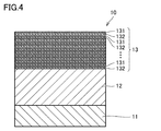
- FIG. 4 is a schematic cross-sectional view of a surface-coated cutting tool according to another aspect of the present embodiment.
- FIG. 5 is a spectrum diagram of the 4f orbit of tungsten element obtained when the WC 1-x layer in this embodiment is measured by X-ray photoelectron spectroscopy.
- the present disclosure has been made in view of the above circumstances, and an object thereof is to provide a surface-coated cutting tool having excellent fracture resistance.
- a surface-coated cutting tool includes: A surface-coated cutting tool comprising a base material and a coating for coating the base material,
- the coating includes a WC 1-x layer made of a compound represented by WC 1-x (where x is 0.54 or more and 0.58 or less),
- the compound represented by WC 1-x includes a hexagonal crystal structure,
- a peak maximum point exists in the range of 31.2 to 31.4 eV.
- the surface-coated cutting tool is provided with excellent toughness by having the above-described configuration. As a result, the surface-coated cutting tool has excellent fracture resistance.
- the WC 1-x layer does not contain metallic tungsten. By defining in this way, it becomes a surface-coated cutting tool with further excellent fracture resistance.
- the WC 1-x layer has a film hardness of 3700 mgf / ⁇ m 2 or more and 4500 mgf / ⁇ m 2 or less.
- the coating further includes a hard coating layer formed on the WC 1-x layer,
- the hard coating layer includes at least a first unit layer having a composition different from that of the WC 1-x layer,
- the first unit layer includes at least one element selected from the group consisting of Group 4 elements, Group 5 elements, Group 6 elements, Al and Si, or at least one of the above elements, and carbon, nitrogen, oxygen And a compound consisting of at least one element selected from the group consisting of boron.
- the first unit layer has a thickness of 0.1 ⁇ m to 10 ⁇ m. By defining in this way, it becomes a surface-coated cutting tool that is further excellent in fracture resistance and wear resistance.
- the hard coating layer further includes a second unit layer having a composition different from that of the WC 1-x layer and the first unit layer,
- the second unit layer includes at least one element selected from the group consisting of Group 4 elements, Group 5 elements, Group 6 elements, Al and Si, or at least one of the above elements, and carbon, nitrogen, oxygen And a compound consisting of at least one element selected from the group consisting of boron and
- the first unit layer and the second unit layer form a multilayer structure in which one or more layers are alternately stacked. By defining in this way, it becomes a surface-coated cutting tool that is further excellent in fracture resistance and wear resistance.
- the first unit layer has a thickness of 1 nm to 100 nm
- the second unit layer has a thickness of 1 nm to 100 nm.
- the film has a thickness of 0.1 ⁇ m or more and 10 ⁇ m or less. By defining in this way, it becomes a surface-coated cutting tool that is further excellent in fracture resistance and wear resistance.
- the base material includes at least one selected from the group consisting of cemented carbide, cermet, high speed steel, ceramics, cBN sintered body, and diamond sintered body.
- the present embodiment is not limited to this.
- the notation in the form of “A to B” means the upper and lower limits of the range (that is, not less than A and not more than B), and there is no unit description in A, and the unit is described only in B.
- the unit of and the unit of B are the same.
- the chemical formula represents any conventionally known composition ratio (element ratio). Shall be included.
- the chemical formula includes not only the stoichiometric composition but also the non-stoichiometric composition.
- the chemical formula of “TiN” includes not only the stoichiometric composition “Ti 1 N 1 ” but also a non-stoichiometric composition such as “Ti 1 N 0.8 ”. The same applies to the description of compounds other than “TiN”.
- the surface-coated cutting tool according to the present disclosure is A surface-coated cutting tool comprising a base material and a coating for coating the base material,
- the coating includes a WC 1-x layer made of a compound represented by WC 1-x (where x is 0.54 or more and 0.58 or less),
- the compound represented by WC 1-x includes a hexagonal crystal structure,
- a peak maximum point exists in the range of 31.2 to 31.4 eV.
- the surface-coated cutting tool of the present embodiment (hereinafter sometimes simply referred to as “cutting tool”) includes a base material and a coating that covers the base material.
- the cutting tool includes, for example, a drill, an end mill, a drill tip changeable cutting tip, an end mill tip replacement cutting tip, a milling tip replacement cutting tip, a turning tip replacement cutting tip, a metal saw, and a gear cutting tool. , Reamer, tap, etc.
- FIG. 1 is a perspective view illustrating an aspect of a surface-coated cutting tool.
- the surface-coated cutting tool having such a shape is used as, for example, a blade-tip-exchangeable cutting tip.
- the surface-coated cutting tool 10 has a rake face 1, a flank face 2, and a cutting edge ridge line portion 3 where the rake face 1 and the flank face 2 intersect. That is, the rake face 1 and the flank face 2 are faces that are connected with the blade edge line portion 3 interposed therebetween.
- the cutting edge ridge line portion 3 constitutes a cutting edge tip portion of the surface-coated cutting tool 10.
- Such a shape of the surface-coated cutting tool 10 can also be grasped as the shape of the base material of the surface-coated cutting tool. That is, the base material has a rake face, a flank face, and a cutting edge ridge line portion connecting the rake face and the flank face.
- the base material is cemented carbide (for example, tungsten carbide (WC) based cemented carbide, cemented carbide containing Co in addition to WC, carbonitride such as Cr, Ti, Ta, Nb in addition to WC).
- cemented carbide for example, tungsten carbide (WC) based cemented carbide, cemented carbide containing Co in addition to WC, carbonitride such as Cr, Ti, Ta, Nb in addition to WC).
- Cermet (mainly composed of TiC, TiN, TiCN, etc.), high speed steel, ceramics (titanium carbide, silicon carbide, silicon nitride, aluminum nitride, aluminum oxide, etc.), cubic crystal It is preferable to include at least one selected from the group consisting of a type boron nitride sintered body (cBN sintered body) and a diamond sintered body, and at least one selected from the group consisting of cemented carbide, cermet and cBN sintered body. More preferably it contains a seed.
- the base material used in this embodiment may have a modified surface.
- a de- ⁇ layer may be formed on the surface, or in the case of cermet, a surface hardened layer may be formed. Even if the surface is modified in this way, this embodiment The effect of is shown.
- the substrate When the surface-coated cutting tool is a cutting edge-exchangeable cutting tip (such as a cutting edge-exchangeable cutting tip for milling), the substrate includes those having a chip breaker and those having no chip breaker.
- the shape of the edge line of the cutting edge is sharp edge (the ridge where the rake face and flank face intersect), honing (the shape with a rounded edge for the sharp edge), negative land (the chamfered shape), and the combination of honing and negative land Any shape is included among the shapes.
- the “coating” according to the present embodiment covers at least a part of the base material (for example, a portion that comes into contact with the work material during cutting), thereby providing various characteristics such as chipping resistance and wear resistance in the cutting tool. It has the effect
- the coating may cover the entire surface of the substrate. In addition, even if a part of the base material is not covered with the coating film or the configuration of the coating film is partially different, it does not depart from the scope of the present embodiment.
- the thickness of the coating is preferably 0.1 ⁇ m or more and 10 ⁇ m or less, more preferably 0.3 ⁇ m or more and 10 ⁇ m or less, further preferably 0.5 ⁇ m or more and 10 ⁇ m or less, and 1 ⁇ m or more and 6 ⁇ m or less. It is still more preferable that it is 1.5 ⁇ m or more and 4 ⁇ m or less.
- the said thickness is less than 0.1 micrometer, there exists a tendency for abrasion resistance to fall.
- the thickness exceeds 10 ⁇ m, peeling or destruction of the coating film tends to occur frequently when a large stress is applied between the coating film and the substrate in intermittent processing.
- the thickness of the coating means the sum of the thicknesses of the respective layers constituting the coating such as a WC 1-x layer, a hard coating layer, and an underlayer which will be described later.
- the thickness of the coating is measured by measuring three arbitrary points in a cross-sectional sample parallel to the normal direction of the surface of the substrate using a transmission electron microscope (TEM), and the measured three-point thickness. It can be obtained by taking the average value of.
- TEM transmission electron microscope
- the transmission electron microscope for example, a spherical aberration corrector JEM-2100F (trade name) manufactured by JEOL Ltd. may be used.
- the coating comprises a WC 1-x layer composed of a compound represented by the WC 1-x.
- “Compound represented by WC 1-x ” (hereinafter sometimes referred to as “WC 1-x ”) means that when the element ratio of tungsten element (W) is 1, the carbon element (C) Tungsten carbide having an element ratio of 1-x is meant.
- the WC 1-x layer may contain inevitable impurities as long as the effects of the surface-coated cutting tool according to the present embodiment are not impaired.
- the content of the inevitable impurities is preferably 0% by mass or more and 0.2% by mass or less with respect to the total mass of the WC 1-x layer.
- the notation of “hard coating layer” and “other layer” to be described later may contain inevitable impurities as long as the effects of the surface-coated cutting tool according to this embodiment are not impaired.
- x is 0.54 or more and 0.58 or less, preferably 0.55 or more and 0.57 or less, and more preferably 0.56 or more and 0.569 or less. If x is less than 0.54, free carbon precipitates at the grain boundaries of WC 1-x and the strength tends to decrease. Further, when x exceeds 0.58, the strength of the crystal grain boundary tends to decrease. Therefore, if x is out of the above range, crack growth cannot be suppressed and the toughness tends to be low. The inventors speculate that such a tendency occurs because the balance between crystal homogeneity and strain is not appropriate.
- the above x is obtained by obtaining a cross-sectional sample parallel to the normal direction of the surface of the base material in the WC 1-x layer, and for the crystal grains appearing in the cross-sectional sample, an incidental to a scanning electron microscope (SEM) or TEM. This can be determined by analyzing using an energy dispersive X-ray spectroscopy (EDX) apparatus. Specifically, each of arbitrary three points in the WC 1-x layer of the cross-sectional sample is measured to obtain the value of x, and the average value of the obtained three points is calculated as WC 1-x of the cross-sectional sample. Let x in the layer. Here, for the “arbitrary three points”, three arbitrary 30 nm ⁇ 30 nm regions in the WC 1-x layer are selected. Examples of the EDX apparatus include a silicon drift detector manufactured by JEOL Ltd., JED-2200 (trade name).
- the compound represented by WC 1-x includes a hexagonal crystal structure.
- the fact that the compound represented by WC 1-x contains a hexagonal crystal structure is analyzed by, for example, performing X-ray diffraction measurement (XRD measurement) on any three points in the WC 1-x layer. This can be confirmed.
- XRD measurement X-ray diffraction measurement
- a peak derived from a crystal plane such as the (102) plane is observed in XRD measurement.
- the apparatus used for the X-ray diffraction measurement include “SmartLab” (trade name) manufactured by Rigaku Corporation, “X′pert” (trade name) manufactured by Panalical, and the like.
- the peak maximum point exists in the range of 31.2 to 31.4 eV in the spectrum diagram of the 4f orbit of tungsten element means that the surface of the WC 1-x layer is analyzed by X-ray photoelectron spectroscopy.
- the spectrum diagram of the 4f orbit of tungsten element obtained directly when measured by the method it means that a peak maximum point exists within the above range (for example, FIG. 5).
- the XPS method is used to determine the bond energy values (eV) at the maximum points at any three points on the surface of the WC 1-x layer. Thereafter, the obtained average value of the three points is set as the value (eV) of the binding energy of “the maximum point of the peak derived from the 4f orbit of the tungsten element” in the WC 1-x layer.
- the above-described measurement is performed after removing the natural oxide layer by Ar + sputtering.
- the measurement is performed after the WC 1-x layer is exposed by Ar + sputtering or the like.
- FIG. 2 is a schematic cross-sectional view of a surface-coated cutting tool in one aspect of the present embodiment.
- the WC 1-x layer 12 may be in contact with the substrate 11.
- the WC 1-x layer 12 may be provided directly on the substrate 11.
- the WC 1-x layer preferably does not contain metallic tungsten.
- the description of “not containing metallic tungsten” includes not only that the WC 1-x layer does not contain metallic tungsten at all, but also those in which metallic tungsten falls below the detection limit.
- the presence or absence of metallic tungsten can be confirmed, for example, by examining the presence or absence of metallic tungsten (presence or absence of a peak derived from metallic tungsten) at any three points of the WC 1-x layer using XRD measurement.
- XRD measurement for example, “SmartLab” (trade name) manufactured by Rigaku Corporation, “X′pert” (trade name) manufactured by Panalical, etc. may be mentioned.
- the WC 1-x layer preferably has a film hardness of 3700 mgf / ⁇ m 2 or more and 4500 mgf / ⁇ m 2 or less, more preferably 3800 mgf / ⁇ m 2 or more and 4300 mgf / ⁇ m 2 or less.
- the film hardness can be measured with a nanoindenter. Specifically, first, each of ten arbitrary points on the surface of the WC 1-x layer is measured to determine the film hardness. Thereafter, the average value of the obtained 10 points of film hardness is taken as the film hardness in the WC 1-x layer of the cross-sectional sample.
- the WC 1-x layer is not the outermost surface, the WC 1-x layer is exposed by mechanical polishing or the like, and then measurement is performed with a nanoindenter.
- the nanoindenter include ENT1100 (trade name) manufactured by Elionix Co., Ltd.
- the WC 1-x layer preferably has a thickness of 0.3 ⁇ m to 7 ⁇ m, and more preferably 0.5 ⁇ m to 3 ⁇ m.
- the coating preferably further includes a hard coating layer formed on the WC 1-x layer.
- the hard coating layer preferably includes at least a first unit layer having a composition different from that of the WC 1-x layer.
- “formed on the WC 1-x layer” means that a hard coating layer is provided on the upper side (the side away from the substrate) of the WC 1-x layer, and is in contact with each other. You don't need to be. In other words, another layer may be provided between the WC 1-x layer and the hard coating layer. Further, as shown in FIG. 3, the hard coating layer 13 may be provided immediately above the WC 1-x layer 12.
- the hard coating layer may be an outermost layer (surface layer).
- the first unit layer includes at least one element selected from the group consisting of Group 4 elements, Group 5 elements, Group 6 elements, Al and Si, or at least one of the above elements, and carbon, nitrogen, oxygen And a compound consisting of at least one element selected from the group consisting of boron and boron.
- the first unit layer is at least one element selected from the group consisting of Cr, Al, Ti and Si, or at least one selected from the group consisting of at least one element described above, and carbon, nitrogen, oxygen and boron. More preferably, it consists of a compound composed of a seed element.
- Examples of the periodic table group 4 element include titanium (Ti), zirconium (Zr), hafnium (Hf), and the like.
- Examples of the periodic table group 5 element include vanadium (V), niobium (Nb), and tantalum (Ta).
- Examples of the periodic table group 6 element include chromium (Cr), molybdenum (Mo), tungsten (W), and the like.
- Examples of the compound contained in the first unit layer include TiAlN, TiAlSiN, TiCrSiN, TiAlCrSiN, AlCrN, AlCrO, AlCrSiN, TiZrN, TiAlMoN, TiAlNbN, TiSiN, AlCrTaN, AlTiVN, TiB 2 , TiCrHfN, CrSiWN, TiAlCTi, AlZrON, AlCrCN, AlHfN, CrSiBON, TiAlWN, AlCrMoCN, TiAlBN, TiAlCrSiBCNO, ZrN and ZrCN.
- the first unit layer (that is, the hard coating layer) has a thickness of 0.1 ⁇ m or more and 10 ⁇ m or less. It is preferably 0.5 ⁇ m or more and 7 ⁇ m or less.
- the hard coating layer preferably further includes a second unit layer having a composition different from that of the WC 1-x layer and the first unit layer.
- the second unit layer includes at least one element selected from the group consisting of Group 4 elements, Group 5 elements, Group 6 elements, Al and Si, or at least one of the above elements, and carbon, nitrogen, oxygen And a compound consisting of at least one element selected from the group consisting of boron and boron.
- the second unit layer is at least one element selected from the group consisting of Cr, Al, Ti, and Si, or at least one selected from the group consisting of carbon, nitrogen, oxygen, and boron, and at least one element selected from the above elements. More preferably, it consists of a compound composed of a seed element. Specific examples of the Group 4 element, the Group 5 element, and the Group 6 element in the periodic table include the elements described above.
- Examples of the compound contained in the second unit layer include the compounds exemplified in the above (first unit layer) column.
- the first unit layer and the second unit layer preferably form a multilayer structure in which one or more layers are alternately laminated. That is, as shown in FIG. 4, the hard coating layer 13 preferably includes a multilayer structure including the first unit layer 131 and the second unit layer 132.
- the multi-layer structure may start to be laminated from either the first unit layer or the second unit layer. That is, the interface on the WC 1-x layer side in the multilayer structure may be constituted by either the first unit layer or the second unit layer. Further, the interface on the side opposite to the WC 1-x layer side in the multilayer structure may be composed of either the first unit layer or the second unit layer.
- the thickness of the hard coating layer is preferably 0.1 ⁇ m or more and 10 ⁇ m or less, and more preferably 0.5 ⁇ m or more and 7 ⁇ m or less.
- the thickness of the first unit layer is preferably 1 nm to 100 nm, and more preferably 2 nm to 25 nm. Furthermore, the thickness of the second unit layer is preferably 1 nm or more and 100 nm or less, and more preferably 2 nm or more and 25 nm or less. In one aspect of this embodiment, when the hard coating layer includes the multilayer structure, the first unit layer has a thickness of 1 nm or more and 100 nm or less, and the second unit layer has a thickness of It is preferably 1 nm or more and 100 nm or less.
- the “thickness of the first unit layer” means the thickness per layer of the first unit layer.
- the “thickness of the second unit layer” means the thickness per layer of the second unit layer.
- the number of layers of the multilayer structure includes an aspect in which the first unit layer and the second unit layer are stacked one by one as long as the thickness of the entire hard coating layer is within the above range.
- both layers may be laminated by 20 to 2500 layers.
- the said film may further contain the other layer.
- the other layers may have different compositions or the same composition as the WC 1-x layer and the hard coating layer.
- Examples of the other layer include a TiN layer and a TiWCN layer. Note that the order of stacking is not particularly limited.
- the other layer includes an underlayer provided between the base material and the WC 1-x layer, and an intermediate layer provided between the WC 1-x layer and the hard coating layer. Layer, a surface layer provided on the hard coating layer, and the like.
- the thickness of the other layers such as the underlayer is not particularly limited as long as the effects of the present embodiment are not impaired, and examples thereof include 0.1 ⁇ m or more and 2 ⁇ m or less.
- the method for manufacturing a surface-coated cutting tool includes a base material preparation step and a WC 1-x layer coating step. Hereinafter, each step will be described.
- the substrate is prepared.
- the base material as described above, any base material can be used as long as it is a conventionally known base material of this type.
- a raw material powder having a predetermined blending composition mass% is uniformly mixed using a commercially available attritor.
- this mixed powder is pressure-molded into a predetermined shape (for example, SEET13T3AGSN, CNMG120408, etc.).
- the above-mentioned base material made of cemented carbide can be obtained by sintering the above-mentioned pressure-formed mixed powder for 1 to 2 hours in a predetermined sintering furnace at 1300 to 1500 ° C. or less.
- a commercial item Sumitomo Electric Hardmetal Co., Ltd. EH520 (brand name) is mentioned, for example.
- ⁇ WC 1-x layer coating process In the WC 1-x layer coating step, at least a part of the surface of the substrate is coated with the WC 1-x layer.
- “at least a part of the surface of the base material” includes a portion that contacts the work material at the time of cutting.
- a method for coating at least a part of the substrate with the WC 1-x layer is not particularly limited, and for example, the WC 1-x layer may be formed by physical vapor deposition (PVD method).
- a conventionally known physical vapor deposition method can be used without any particular limitation.
- Examples of such physical vapor deposition include sputtering, ion plating, arc ion plating, and electron ion beam vapor deposition.
- the cathode arc ion plating method or sputtering method with a high ion ratio of the raw material element is used, it becomes possible to perform metal or gas ion bombardment treatment on the substrate surface before forming the coating film. This is preferable because the adhesiveness is greatly improved.
- a WC target for example, a sintered or melted target having a composition of WC and a C content of 3 to 6.1% by mass
- a substrate base material
- argon gas is introduced as the gas.
- the substrate (negative) bias voltage at 10 to 700 V and DC or pulse DC (frequency 10 to 300 kHz)
- an arc current of 80 to 150 A is supplied to the cathode electrode, and metal ions and the like are supplied from the arc evaporation source.
- the substrate temperature is preferably set to 550 to 600 ° C. in the initial stage of formation of the WC 1-x layer (the film thickness is in the range of 0.2 ⁇ m or less).
- AIP (trade name) manufactured by Kobe Steel, Ltd. may be mentioned.
- the method for manufacturing a surface-coated cutting tool according to this embodiment preferably further includes a hard coating layer coating step after the WC 1-x layer coating step.
- the method for forming the hard coating layer is not particularly limited, and a conventional method can be used. Specifically, for example, a hard coating layer is formed by the PVD method described above.
- a base layer coating step of forming a base layer between a base material and the WC 1-x layer, the WC 1-x layer, and the hard coating An intermediate layer coating step for forming an intermediate layer between the layers, a surface layer coating step for forming a surface layer on the hard coating layer, a surface treatment step, and the like may be appropriately performed.
- other layers such as the above-described underlayer, intermediate layer, and surface layer are formed, other layers may be formed by a conventional method.
- the above-mentioned other layer is formed by the PVD method described above.
- the surface treatment step include surface treatment using a medium in which diamond powder is supported on an elastic material.
- the apparatus for performing the surface treatment include Sirius Z manufactured by Fuji Seisakusho Co., Ltd.
- JIS standard K10 carbide shape: JIS standard CNMG120408
- the base material was set at a predetermined position of an arc ion plating apparatus (trade name: AIP, manufactured by Kobe Steel, Ltd.).
- a WC 1-x layer coating process As a WC 1-x layer coating step, a WC 1-x layer was formed on the substrate by arc ion plating. Specifically, the following method was used. First, a WC target (a sintered or melted target having a composition of WC and a C content of 3 to 6.1% by mass) was set in an arc evaporation source of an arc ion plating apparatus. Next, the substrate temperature was set to 400 to 550 ° C., and the gas pressure in the apparatus was set to 1.0 to 3.5 Pa. Argon gas was introduced as the gas.
- a WC target a sintered or melted target having a composition of WC and a C content of 3 to 6.1% by mass
- an arc current of 80 to 150 A was supplied to the cathode electrode while maintaining the substrate (negative) bias voltage at 10 to 700 V and DC or pulse DC (frequency 10 to 300 kHz).
- a WC 1-x layer was formed by generating metal ions and the like from an arc evaporation source by supplying an arc current.
- the substrate temperature was set to 550 to 600 ° C.
- a bias having a high frequency of 250 to 300 kHz ⁇ high voltage of 600 to 700 V was intermittently applied over a film thickness of 30 nm or less throughout the film formation.
- ⁇ Underlayer coating process> For the samples (Examples 12, 13, 15 and 16) in which the base layer was provided between the base material and the WC 1-x layer, the substrate was subjected to the following procedure before the WC 1-x layer coating step. An underlayer was formed on the material. First, a target (sintered target or melted target) containing a metal composition in the column of the underlayer composition shown in Table 1 was set in an arc evaporation source of an arc ion plating apparatus. Next, the substrate temperature was set to 400 to 650 ° C., and the gas pressure in the apparatus was set to 0.8 to 5 Pa. As a reaction gas, a mixed gas of nitrogen gas and argon gas was introduced in the case of a nitride underlayer.
- ⁇ Hard coating layer coating process> Further, for samples (Examples 12, 13, 15 and 16) in which a hard coating layer on a WC 1-x layer, the following procedure after the WC 1-x layer coating process, WC 1 A hard coating layer was formed on the ⁇ x layer, and a surface-coated cutting tool according to this embodiment was produced.
- a target sintered target or melt target
- the substrate temperature was set to 500 to 650 ° C.
- the gas pressure in the apparatus was set to 0.8 to 5.0 Pa.
- a mixed gas of nitrogen gas and argon gas was introduced in the case of a nitride hard coating layer.
- a mixed gas of nitrogen gas, methane gas, and argon gas was introduced as a reaction gas.
- a mixed gas of oxygen gas and argon gas was introduced as the reaction gas.
- an arc current of 80 to 150 A was supplied to the cathode electrode.
- a hard coating layer was formed to a thickness shown in Table 1 by generating metal ions and the like from an arc evaporation source by supplying an arc current.
- the composition x of the WC 1-x layer was determined by using an EDX device attached to the TEM (silicon drift detector manufactured by JEOL Ltd., trade name: JED-2200) using a cross-sectional sample parallel to the normal direction of the surface of the substrate. ) was measured under the following conditions. Specifically, first, each of arbitrary three points in the WC 1-x layer of the cross-sectional sample was measured to obtain the value of the composition x. Thereafter, the average value of the obtained three points was set as the composition x in the WC 1-x layer of the cross-sectional sample. Here, as the “arbitrary three points”, three arbitrary 30 nm ⁇ 30 nm regions in the WC 1-x layer were selected. The results are shown in Table 1. Measurement conditions for EDX method Acceleration voltage: 200 kV Probe current: 0.29 nA Probe size: 0.2 nm
- the value of the binding energy at the maximum point of the spectrum peak (XPS W4f peak) of the tungsten element in the WC 1-x layer was obtained as follows. First, using the apparatus used in the XPS method (trade name: Versa Probe III, manufactured by ULVAC-PHI Co., Ltd.), the value of the binding energy of the maximum point at any three points on the surface of the WC 1-x layer ( eV) was determined (for example, FIG. 5). Thereafter, the average value of the obtained three points was used as the value of the binding energy of “the peak maximum of the spectrum of the 4f orbital of tungsten element” in the WC 1-x layer.
- Neutralizing gun Dual type Ar + : Acceleration voltage 4kV Raster size: 1 ⁇ 1mm Sputtering speed (Ar + ): SiO 2 sputtering conversion value 28.3 nm / min
- the film hardness of the WC 1-x layer was measured using a nanoindenter (trade name: ENT1100, manufactured by Elionix Co., Ltd.) under the following conditions. At this time, the film hardness was first determined by measuring each of 10 arbitrary points on the surface of the WC 1-x layer. Thereafter, the average value of the obtained ten points of film hardness was taken as the film hardness in the WC 1-x layer. When the WC 1-x layer was not the outermost surface, the WC 1-x layer was exposed by mechanical polishing or the like, and then measured with a nanoindenter. The results are shown in Table 1. Measurement conditions of nano indenter Indenter: Berkovich load: 1 gf Load time: 10,000 msec Holding time: 2000 msec Unloading time: 10000msec
- the thickness of the WC 1-x layer, the underlayer, the hard coating layer (first unit layer, second unit layer) and the coating were determined as follows. First, using a transmission electron microscope (TEM) (manufactured by JEOL Ltd., trade name: JEM-2100F), arbitrary three points in a cross-sectional sample parallel to the normal direction of the surface of the substrate were measured. Then, it calculated
- TEM transmission electron microscope
- TiAlSiN (8 nm) / TiSiN (4 nm) multilayer structure (1.0 ⁇ m)” in the “hard coating layer” indicates that the hard coating layer has a thickness of 8 nm thick TiAlSiN layer (first unit layer).
- the figure shows that a TiSiN layer (second unit layer) having a thickness of 4 nm is formed in a multilayer structure (total thickness: 1.0 ⁇ m) in which 84 layers are stacked alternately one above the other.
Landscapes
- Chemical & Material Sciences (AREA)
- Organic Chemistry (AREA)
- Engineering & Computer Science (AREA)
- Materials Engineering (AREA)
- Mechanical Engineering (AREA)
- Metallurgy (AREA)
- Chemical Kinetics & Catalysis (AREA)
- Inorganic Chemistry (AREA)
- Life Sciences & Earth Sciences (AREA)
- Wood Science & Technology (AREA)
- Ceramic Engineering (AREA)
- Cutting Tools, Boring Holders, And Turrets (AREA)
- Drilling Tools (AREA)
- Physical Vapour Deposition (AREA)
Abstract
Priority Applications (5)
| Application Number | Priority Date | Filing Date | Title |
|---|---|---|---|
| CN201980002653.4A CN110691663B (zh) | 2018-03-19 | 2019-03-14 | 表面被覆切削工具 |
| JP2019554423A JP6798626B2 (ja) | 2018-03-19 | 2019-03-14 | 表面被覆切削工具 |
| US16/615,465 US20200171581A1 (en) | 2018-03-19 | 2019-03-14 | Surface-coated cutting tool |
| EP19771216.9A EP3769877A4 (fr) | 2018-03-19 | 2019-03-14 | Outil de coupe revêtu en surface |
| KR1020197034798A KR20200131157A (ko) | 2018-03-19 | 2019-03-14 | 표면 피복 절삭 공구 |
Applications Claiming Priority (2)
| Application Number | Priority Date | Filing Date | Title |
|---|---|---|---|
| JP2018051012 | 2018-03-19 | ||
| JP2018-051012 | 2018-03-19 |
Publications (1)
| Publication Number | Publication Date |
|---|---|
| WO2019181740A1 true WO2019181740A1 (fr) | 2019-09-26 |
Family
ID=67986265
Family Applications (1)
| Application Number | Title | Priority Date | Filing Date |
|---|---|---|---|
| PCT/JP2019/010612 Ceased WO2019181740A1 (fr) | 2018-03-19 | 2019-03-14 | Outil de coupe revêtu en surface |
Country Status (6)
| Country | Link |
|---|---|
| US (1) | US20200171581A1 (fr) |
| EP (1) | EP3769877A4 (fr) |
| JP (1) | JP6798626B2 (fr) |
| KR (1) | KR20200131157A (fr) |
| CN (1) | CN110691663B (fr) |
| WO (1) | WO2019181740A1 (fr) |
Cited By (2)
| Publication number | Priority date | Publication date | Assignee | Title |
|---|---|---|---|---|
| WO2022244190A1 (fr) * | 2021-05-20 | 2022-11-24 | 住友電工ハードメタル株式会社 | Outil de coupe |
| US12605770B2 (en) | 2021-05-20 | 2026-04-21 | Sumitomo Electric Hardmetal Corp. | Cutting tool |
Families Citing this family (3)
| Publication number | Priority date | Publication date | Assignee | Title |
|---|---|---|---|---|
| JP7618814B2 (ja) * | 2021-07-30 | 2025-01-21 | 京セラ株式会社 | 被覆工具および切削工具 |
| CN115595532B (zh) * | 2022-10-12 | 2024-11-12 | 株洲华锐精密工具股份有限公司 | 一种多层结构硬质涂层及其制备方法与应用 |
| CN119325413A (zh) * | 2023-05-17 | 2025-01-17 | 住友电气工业株式会社 | 切削工具 |
Citations (10)
| Publication number | Priority date | Publication date | Assignee | Title |
|---|---|---|---|---|
| JPS5939243B2 (ja) * | 1978-08-07 | 1984-09-21 | 三菱マテリアル株式会社 | 表面被覆工具部品 |
| JPS6257802A (ja) * | 1985-09-05 | 1987-03-13 | Sumitomo Electric Ind Ltd | 硬質炭素被覆部品 |
| JPH0679503A (ja) * | 1992-06-30 | 1994-03-22 | Kyocera Corp | 超硬質膜付工具及びその製造方法 |
| JPH06262405A (ja) | 1993-03-05 | 1994-09-20 | Toshiba Tungaloy Co Ltd | 工具用被覆部品 |
| JP2001150206A (ja) * | 1999-11-29 | 2001-06-05 | Mitsubishi Materials Corp | 断続重切削ですぐれた耐欠損性を発揮する表面被覆炭化タングステン基超硬合金製切削工具 |
| JP2003527293A (ja) * | 2000-03-15 | 2003-09-16 | ハーダイド・リミテツド | ダイアモンド用およびダイアモンド含有材料用の接着性複合被膜および前記被膜の製造方法 |
| US6800383B1 (en) * | 1999-02-11 | 2004-10-05 | Hardide Limited | Tungsten carbide coating and method for producing the same |
| WO2012056758A1 (fr) * | 2010-10-28 | 2012-05-03 | 住友電工ハードメタル株式会社 | Compact fritté revêtu en surface |
| WO2014003172A1 (fr) * | 2012-06-29 | 2014-01-03 | 株式会社神戸製鋼所 | Corps moulé en film à base de cda |
| JP2018051012A (ja) | 2016-09-29 | 2018-04-05 | サミー株式会社 | ぱちんこ遊技機 |
Family Cites Families (2)
| Publication number | Priority date | Publication date | Assignee | Title |
|---|---|---|---|---|
| BR102012003607A2 (pt) * | 2012-02-16 | 2013-10-29 | Mahle Metal Leve Sa | Componente deslizante para uso em motores de combustão interna |
| JP6663244B2 (ja) * | 2016-02-16 | 2020-03-11 | イビデン株式会社 | 透光板及びその製造方法 |
-
2019
- 2019-03-14 WO PCT/JP2019/010612 patent/WO2019181740A1/fr not_active Ceased
- 2019-03-14 US US16/615,465 patent/US20200171581A1/en not_active Abandoned
- 2019-03-14 JP JP2019554423A patent/JP6798626B2/ja active Active
- 2019-03-14 KR KR1020197034798A patent/KR20200131157A/ko not_active Withdrawn
- 2019-03-14 CN CN201980002653.4A patent/CN110691663B/zh active Active
- 2019-03-14 EP EP19771216.9A patent/EP3769877A4/fr active Pending
Patent Citations (10)
| Publication number | Priority date | Publication date | Assignee | Title |
|---|---|---|---|---|
| JPS5939243B2 (ja) * | 1978-08-07 | 1984-09-21 | 三菱マテリアル株式会社 | 表面被覆工具部品 |
| JPS6257802A (ja) * | 1985-09-05 | 1987-03-13 | Sumitomo Electric Ind Ltd | 硬質炭素被覆部品 |
| JPH0679503A (ja) * | 1992-06-30 | 1994-03-22 | Kyocera Corp | 超硬質膜付工具及びその製造方法 |
| JPH06262405A (ja) | 1993-03-05 | 1994-09-20 | Toshiba Tungaloy Co Ltd | 工具用被覆部品 |
| US6800383B1 (en) * | 1999-02-11 | 2004-10-05 | Hardide Limited | Tungsten carbide coating and method for producing the same |
| JP2001150206A (ja) * | 1999-11-29 | 2001-06-05 | Mitsubishi Materials Corp | 断続重切削ですぐれた耐欠損性を発揮する表面被覆炭化タングステン基超硬合金製切削工具 |
| JP2003527293A (ja) * | 2000-03-15 | 2003-09-16 | ハーダイド・リミテツド | ダイアモンド用およびダイアモンド含有材料用の接着性複合被膜および前記被膜の製造方法 |
| WO2012056758A1 (fr) * | 2010-10-28 | 2012-05-03 | 住友電工ハードメタル株式会社 | Compact fritté revêtu en surface |
| WO2014003172A1 (fr) * | 2012-06-29 | 2014-01-03 | 株式会社神戸製鋼所 | Corps moulé en film à base de cda |
| JP2018051012A (ja) | 2016-09-29 | 2018-04-05 | サミー株式会社 | ぱちんこ遊技機 |
Non-Patent Citations (1)
| Title |
|---|
| See also references of EP3769877A4 |
Cited By (2)
| Publication number | Priority date | Publication date | Assignee | Title |
|---|---|---|---|---|
| WO2022244190A1 (fr) * | 2021-05-20 | 2022-11-24 | 住友電工ハードメタル株式会社 | Outil de coupe |
| US12605770B2 (en) | 2021-05-20 | 2026-04-21 | Sumitomo Electric Hardmetal Corp. | Cutting tool |
Also Published As
| Publication number | Publication date |
|---|---|
| KR20200131157A (ko) | 2020-11-23 |
| EP3769877A4 (fr) | 2021-07-14 |
| CN110691663B (zh) | 2020-09-01 |
| JP6798626B2 (ja) | 2020-12-09 |
| JPWO2019181740A1 (ja) | 2020-07-27 |
| US20200171581A1 (en) | 2020-06-04 |
| CN110691663A (zh) | 2020-01-14 |
| EP3769877A1 (fr) | 2021-01-27 |
Similar Documents
| Publication | Publication Date | Title |
|---|---|---|
| JP6813103B2 (ja) | 表面被覆切削工具 | |
| JP6798627B2 (ja) | 表面被覆切削工具 | |
| JP6798626B2 (ja) | 表面被覆切削工具 | |
| JP7354933B2 (ja) | 切削工具 | |
| JP7622344B2 (ja) | 切削工具 | |
| CN114929415B (zh) | 切削工具 | |
| JP7574906B2 (ja) | 切削工具 | |
| CN120603665A (zh) | 切削工具 | |
| JP7443655B2 (ja) | 切削工具 | |
| CN115666830B (zh) | 切削工具 | |
| JP7251347B2 (ja) | 表面被覆切削工具 | |
| JP7251348B2 (ja) | 表面被覆切削工具 | |
| CN119325413A (zh) | 切削工具 | |
| WO2022244190A1 (fr) | Outil de coupe | |
| WO2022244191A1 (fr) | Outil de coupe |
Legal Events
| Date | Code | Title | Description |
|---|---|---|---|
| ENP | Entry into the national phase |
Ref document number: 2019554423 Country of ref document: JP Kind code of ref document: A |
|
| 121 | Ep: the epo has been informed by wipo that ep was designated in this application |
Ref document number: 19771216 Country of ref document: EP Kind code of ref document: A1 |
|
| ENP | Entry into the national phase |
Ref document number: 20197034798 Country of ref document: KR Kind code of ref document: A |
|
| NENP | Non-entry into the national phase |
Ref country code: DE |
|
| ENP | Entry into the national phase |
Ref document number: 2019771216 Country of ref document: EP Effective date: 20201019 |