WO2019189105A1 - Commutateur multidiffusion - Google Patents
Commutateur multidiffusion Download PDFInfo
- Publication number
- WO2019189105A1 WO2019189105A1 PCT/JP2019/012731 JP2019012731W WO2019189105A1 WO 2019189105 A1 WO2019189105 A1 WO 2019189105A1 JP 2019012731 W JP2019012731 W JP 2019012731W WO 2019189105 A1 WO2019189105 A1 WO 2019189105A1
- Authority
- WO
- WIPO (PCT)
- Prior art keywords
- optical
- optical switch
- switch
- output
- row
- Prior art date
- Legal status (The legal status is an assumption and is not a legal conclusion. Google has not performed a legal analysis and makes no representation as to the accuracy of the status listed.)
- Ceased
Links
Images


Classifications
-
- G—PHYSICS
- G02—OPTICS
- G02B—OPTICAL ELEMENTS, SYSTEMS OR APPARATUS
- G02B6/00—Light guides; Structural details of arrangements comprising light guides and other optical elements, e.g. couplings
- G02B6/24—Coupling light guides
- G02B6/26—Optical coupling means
- G02B6/35—Optical coupling means having switching means
- G02B6/354—Switching arrangements, i.e. number of input/output ports and interconnection types
- G02B6/356—Switching arrangements, i.e. number of input/output ports and interconnection types in an optical cross-connect device, e.g. routing and switching aspects of interconnecting different paths propagating different wavelengths to (re)configure the various input and output links
-
- G—PHYSICS
- G02—OPTICS
- G02B—OPTICAL ELEMENTS, SYSTEMS OR APPARATUS
- G02B6/00—Light guides; Structural details of arrangements comprising light guides and other optical elements, e.g. couplings
- G02B6/10—Light guides; Structural details of arrangements comprising light guides and other optical elements, e.g. couplings of the optical waveguide type
- G02B6/12—Light guides; Structural details of arrangements comprising light guides and other optical elements, e.g. couplings of the optical waveguide type of the integrated circuit kind
- G02B6/122—Basic optical elements, e.g. light-guiding paths
- G02B6/1223—Basic optical elements, e.g. light-guiding paths high refractive index type, i.e. high-contrast waveguides
-
- G—PHYSICS
- G02—OPTICS
- G02B—OPTICAL ELEMENTS, SYSTEMS OR APPARATUS
- G02B6/00—Light guides; Structural details of arrangements comprising light guides and other optical elements, e.g. couplings
- G02B6/24—Coupling light guides
- G02B6/26—Optical coupling means
- G02B6/35—Optical coupling means having switching means
- G02B6/3596—With planar waveguide arrangement, i.e. in a substrate, regardless if actuating mechanism is outside the substrate
-
- G—PHYSICS
- G02—OPTICS
- G02F—OPTICAL DEVICES OR ARRANGEMENTS FOR THE CONTROL OF LIGHT BY MODIFICATION OF THE OPTICAL PROPERTIES OF THE MEDIA OF THE ELEMENTS INVOLVED THEREIN; NON-LINEAR OPTICS; FREQUENCY-CHANGING OF LIGHT; OPTICAL LOGIC ELEMENTS; OPTICAL ANALOGUE/DIGITAL CONVERTERS
- G02F1/00—Devices or arrangements for the control of the intensity, colour, phase, polarisation or direction of light arriving from an independent light source, e.g. switching, gating or modulating; Non-linear optics
- G02F1/29—Devices or arrangements for the control of the intensity, colour, phase, polarisation or direction of light arriving from an independent light source, e.g. switching, gating or modulating; Non-linear optics for the control of the position or the direction of light beams, i.e. deflection
- G02F1/31—Digital deflection, i.e. optical switching
- G02F1/313—Digital deflection, i.e. optical switching in an optical waveguide structure
-
- G—PHYSICS
- G02—OPTICS
- G02B—OPTICAL ELEMENTS, SYSTEMS OR APPARATUS
- G02B6/00—Light guides; Structural details of arrangements comprising light guides and other optical elements, e.g. couplings
- G02B6/10—Light guides; Structural details of arrangements comprising light guides and other optical elements, e.g. couplings of the optical waveguide type
- G02B6/12—Light guides; Structural details of arrangements comprising light guides and other optical elements, e.g. couplings of the optical waveguide type of the integrated circuit kind
- G02B2006/12133—Functions
- G02B2006/12145—Switch
-
- G—PHYSICS
- G02—OPTICS
- G02B—OPTICAL ELEMENTS, SYSTEMS OR APPARATUS
- G02B6/00—Light guides; Structural details of arrangements comprising light guides and other optical elements, e.g. couplings
- G02B6/24—Coupling light guides
- G02B6/26—Optical coupling means
- G02B6/35—Optical coupling means having switching means
- G02B6/354—Switching arrangements, i.e. number of input/output ports and interconnection types
- G02B6/3544—2D constellations, i.e. with switching elements and switched beams located in a plane
- G02B6/3546—NxM switch, i.e. a regular array of switches elements of matrix type constellation
Definitions
- the present invention relates to an optical switch. Specifically, the present invention relates to a multicast switch that can be used in an optical communication system.
- ROADM Reconfigurable Optical Add / Drop Multiplexer
- ROADM Reconfigurable Optical Add / Drop Multiplexer
- MCS multicast switch
- optical splitter optical coupler
- optical switch which are small optical devices
- MCS wavelength selective switches and matrix optical switches
- MZI optical switch Mach-Zehnder interferometer type 2 ⁇ 2 optical switch
- silica-based waveguide there is a Mach-Zehnder interferometer type 2 ⁇ 2 optical switch (MZI optical switch) using a silica-based waveguide.
- the MZI optical switch is provided with a thermo-optic phase shifter (thin film heater) in the vicinity of the two arm waveguides, and the path through which the optical signal passes can be changed by controlling on / off of the thin film heater.
- FIG. 1 is a diagram illustrating a conventional MZI optical switch.
- the MZI optical switch of FIG. 1 includes input optical waveguides 11a and 11b, thin film heaters 12a and 12b, directional couplers 13-1 and 13-2, two arm waveguides 14a and 14b, and a thin film heater 12a. , 12b, lead wires 15a to 15d as drive electric wires for supplying power, and output optical waveguides 16a and 16b.
- one of the input optical waveguides 11a and 11b is an unconnected waveguide
- the MZI optical switch is used as a 2 ⁇ 1 optical switch
- the output optical waveguides 16a and 16b are used. One of these becomes an unconnected waveguide.
- the two arm waveguides 14a and 14b are usually designed to have a half-wavelength optical path length difference. Therefore, when the half-wavelength optical path length difference between the two arm waveguides 14a and 14b is not canceled without driving (feeding) the thin film heaters 12a and 12b, the optical signal path is a bar path (input optical waveguide). 11a ⁇ output optical waveguide 16a, input optical waveguide 11b ⁇ output optical waveguide 16b). When the thin film heaters 12a and 12b are driven to cancel the optical path length difference of the half wavelength by the thermo-optic effect, the optical signal path is a cross path (input optical waveguide 11a ⁇ output optical waveguide 16b, input optical waveguide).
- the MZI optical switch shown in FIG. Accordingly, by controlling the power feeding by the lead wires 15a to 15d, the on / off of the MZI optical switch can be controlled through the on / off of the driving of the thin film heaters 12a, 12b.
- FIG. 2 is a diagram illustrating an MCS configured with a conventional 4-input 4-output MCS (hereinafter referred to as 4 ⁇ 4 MCS) using an MZI optical switch.
- FIG. 2 shows four input ports In 1 to In 4 and output ports Out 1 to Out 4 each connected to an optical waveguide, a 1 ⁇ 2 splitter SP, and a gate switch GSW 1,1 which is a 1 ⁇ 2 switch.
- GSW 4,4 main switches MSW 1,1 to MSW 4,4 which are 2 ⁇ 1 switches, lead lines 15 for controlling on / off of GSW and MSW, and ground for grounding GSW and MSW An MCS with line 17 is shown.
- MZI optical switches as shown in FIG. 1 are used.
- the bend radius of the optical waveguide is large, and in order to reduce the size, a structure in which the longitudinal direction is shortened rather than a structure to be bent is advantageous. For this reason, it has been necessary to adopt a configuration (nested arrangement) in which the gaps are alternately filled in the GSW and MSW in the vertical direction.
- the 1 ⁇ 2 splitter SP is an asymmetric splitter, and the demultiplexing ratio is set to 3: 1, 2: 1, and 1: 1 in order from the 1 ⁇ 2 splitter SP in the first column to the next column. . This is to prevent a difference in optical output between the output ports.
- the optical switch unit SU is divided into the configuration of SUa illustrated in FIG. 3 and the configuration of SUb illustrated in FIG.
- FIG. 3 is a diagram illustrating the configuration of a conventional SUa.
- FIG. 3 shows a SUa including a 1 ⁇ 2 splitter SP, a GSW, and an MSW.
- SUa is a 1 ⁇ 2 switch that combines a splitter having first and second input terminals a and b and first and second output terminals c and d.
- FIG. 4 is a diagram illustrating the configuration of a conventional SUb.
- FIG. 4 shows the SUb including the gate switch GSW, the main switch MSW, and the lead line 15.
- SUb is a 2 ⁇ 1 switch having first and second input terminals a and b and an output terminal d.
- GSW and MSW are connected to different lead lines 15 and ground lines 17, respectively.
- MSW inputs the first optical signal from the first input terminal a of the SUb via the GSW, and inputs the second optical signal from the second input terminal b of the SUb.
- the MSW is in the bar state in the off state, and outputs the second optical signal to the output end d of the SUb.
- the MSW In the on state, the MSW is in the cross state and sends the second optical signal to the terminating waveguide e.
- the first optical signal is output to the output end d of the SUb.
- the lead-out direction of the lead-out line 15 depends on the necessity of laying out the lead-out line 15 without intersecting on the substrate, and the ease of work / process. The direction is perpendicular to the input / output direction. For this reason, there is a problem that 32 lead lines 15 are arranged in a row and a large area is occupied by the 32 lead lines 15.
- M ⁇ NMCS (M ⁇ N) ⁇ 2 lead lines are required, so as the number of input / output ports increases, the number of lead lines also increases, and the occupied area becomes larger. There was a problem.
- the present invention has been made in view of such problems, and an object thereof is to provide a small multicast switch with a reduced number of lead lines.
- a multicast switch includes M input ports for inputting optical signals, each of which is associated with a different one of the first numbers 1,. .., N each associated with a different one of N output ports from which the optical signal is output and M ⁇ N optical switches each associated with a different number of sets [m, n] Wherein m is an integer 1 ⁇ m ⁇ M corresponding to the first number, and n is an integer 1 ⁇ n ⁇ N corresponding to the second number.
- Each optical switch unit And a connected lead wire is formed on the high refractive index waveguide substrate, and one of the M ⁇ N optical switch units is turned on to turn on the optical switch unit.
- the optical signal input to the input port associated with the first number associated with the optical switch unit in the state is associated with the second number associated with the optical switch unit in the on state.
- a multicast switch that is output from an output port, wherein the M ⁇ N optical switch units are at least a gate switch that is a 1 ⁇ 1 switch and a 2 ⁇ 1 switch that is provided in a subsequent stage of the gate switch.
- Lead line is characterized by a common.
- FIG. 5 is a diagram for explaining the operation of 4 ⁇ 4 MCS. In FIG. 5, wiring is omitted and not shown. FIG. 5 shows 16 SU 1,1 to SU 4,4 .
- SU 3,1 , SU 4,2 , SU 1,3 , SU 2,4 respectively connected to the output ports Out 1 to Out 4 are SUb, and the others are SUa.
- the optical signal input from SUa is output from the output side SUb via two SUa.
- all the optical signals of the input ports In 1 to In 4 are not output to the output ports Out 1 to Out 4 because they are connected to the termination waveguide e.
- the optical signal of the input port In 1 is not output to the output ports Out 1 to Out 4 because it is connected to the termination waveguide e at SU 1,3 .
- the input ports In 2 to In 4 are not output to the output ports Out 1 to Out 4 because they are connected to the termination waveguide e by SU 2,4 , SU 3,1 and SU 4,2 respectively.
- a voltage may be applied to SU 2,3 .
- the optical signal from the input port In 2 passes through the SU 2,2 and SU 2,1 in the bar state to the SU 1,3 in the bar state from the SU 2,3 in the on state. is output from the output port Out 3 through.
- the cross state (connected to the terminating waveguide) is set, and in the voltage applied state, the bar state (transmitting state) is set. It becomes the layout figure shown.
- the SU is composed of M ⁇ (N ⁇ 1) optical switch units (SUa) and M optical switch units (SUb) connected to the output ports.
- M ⁇ N ⁇ 1 optical switch units
- SUb M optical switch units
- FIG. 7 is a diagram illustrating an example in which the configuration of the M ⁇ NMCS 100 (M and N are each an integer of 2 or more) according to the first embodiment of the present invention is simplified.
- FIG. 7 shows M input ports In 1 to In M for inputting optical signals, N output ports Out 1 to Out N for outputting optical signals, and M ⁇ N optical switch units SU110.
- the optical waveguide 101 for optically connecting the input ports In 1 to In M and the SU 110 and the output ports Out 1 to Out N and the SU 110 are connected to the SU 110 so as to control the on / off of each SU 110 by supplying power to each SU 110.
- the M ⁇ NMCS 100 is shown in which the M ⁇ N lead wires 115 and the ground wire 117 for grounding the SU 110 are formed on the high refractive index waveguide substrate.
- the M ⁇ NMCS 100 includes a plurality of optical switch unit columns (hereinafter referred to as SU columns) 140, and the SU column 140 is a vertical column (parallel to the lead lines 115 and the ground 117). Includes a plurality of SUs 110 arranged in a row.
- a ground line 117 is arranged in parallel with each SU row 140, and the ground line 117 arranged in parallel with each SU 110 of each SU row 140 is connected to each other.
- Each SU 110 includes a GSW that is a 1 ⁇ 1 switch and an MSW that is a 2 ⁇ 1 switch provided in a subsequent stage of the GSW.
- a plurality of GSWs and a plurality of MSWs included in each SU 110 are arranged in columns, and constitute a GSW column 120 and an MSW column 130.
- the GSW and MSW included in the SU 110 are connected to the same lead line.
- the SUs 110 are linearly arranged vertically and horizontally on the high refractive index waveguide substrate, and are arranged in a lattice pattern.
- each SU 110 may shift its position as long as it is within the allowable range of the electrical wiring layout such as a common lead line.
- the GSW row 120 and the MSW row 130 are alternately arranged from the input port to the output port, the GSW is connected to the input ports In 1 to In M , and the output ports Out 1 to Out N Is connected to the MSW.
- FIGS. 8 and 9 are diagrams respectively illustrating the configurations of SUa and SUb according to the first embodiment of the present invention.
- GSW and MSW are connected in series by a common lead line 115 and a ground line 117, and are simultaneously controlled on and off.
- the wirings of GSW and MSW are laid out so as to be connected without intersecting.
- the SUa and SUb according to the first embodiment are the same as the SUa and SUb shown in FIGS. 3 and 4 except that they are connected by the common lead line 115 and the ground line 117.
- the SUs connected to Out 1 to Out N are the SUb illustrated in FIG. 9, and the other Sus are This is the SUa shown in FIG. 8 (the 1 ⁇ 2 splitter SP connected to the previous stage of SUa is omitted for simplicity). Also in the following embodiments, SUa and SUb have the same configuration as SUa and SUb shown in FIGS. 8 and 9.
- one of the M ⁇ N SUs is turned on to be input to the input port associated with the first number associated with the SU in the on state.
- the optical signal is output from the output port associated with the second number associated with the ON state SU.
- the optical signal input to the input port In m can be output from the output port Out n by turning on the SU associated with an arbitrary number [m, n].
- FIGS. 10 and 11 are diagrams showing other examples of the configurations of SUa and SUb according to the first embodiment of the present invention, respectively.
- GSW and MSW may be connected in parallel by a common lead line 115 and ground line 117.
- FIGS. 12 and 13 are diagrams respectively showing still other examples of the configurations of SUa and SUb according to the first embodiment of the present invention.
- 12 and 13 show SUa and SUb including two or more GSW 1 to GSW N.
- a plurality of GSW 1 to GSW N and MSW are connected in parallel by a common lead-out line 115 and ground line 117, and are simultaneously turned on / off.
- the light that leaks when the first-stage GSW 1 is turned off can be blocked by the subsequent-stage GSW, thereby reducing noise. It becomes possible to do. Further, according to the example shown in FIGS. 12 and 13, it is possible to reduce the number of wirings by N with respect to the number N of GSWs as compared with the case where the number of GSWs is increased by a conventional method in which the lead lines are not shared. Become.
- FIGS. 14 and 15 are diagrams illustrating still another example of the configuration of SUa and SUb according to the first embodiment of the present invention.
- a plurality of GSW 1 to GSW N and MSW are connected in parallel.
- the present invention is not limited to this, and a plurality of GSW 1 to GSW N and MSW may be connected in series by a common lead-out line 115 and ground line 117 as in the example shown in FIGS.
- the number of lead lines can be halved compared to the conventional configuration. Can be realized.
- FIG. 16 is a diagram illustrating an example in which the configuration of the M ⁇ NMCS 200 according to the second embodiment of the present invention is simplified.
- FIG. 16 shows M input ports In 1 to In M for inputting optical signals, N output ports Out 1 to Out N for outputting optical signals, M ⁇ N SUs 210, and input ports.
- An optical waveguide 201 that optically connects between In 1 to In M , SU 210 and output ports Out 1 to Out N, and M ⁇ N lead lines 215 respectively connected to each SU 210 so as to perform on / off control of each SU 210 , M ⁇ NMCS 200 is shown in which a ground line 217 for grounding SU 210 is formed on a high refractive index waveguide substrate.
- the M ⁇ NMCS 200 includes a plurality of SU columns 240 including SU columns 240 1 to 240 x , and each SU column 240 includes a plurality of SUs 210 arranged in columns. Configured.
- the M ⁇ NMCS 200 includes a folded waveguide portion 202 formed by folding the optical waveguide 201 between adjacent SU rows 240.
- x which is the number of columns of the SU column 240, is an even number of 2 or more.
- the SU row 250 includes at least one of M + M, M + N, and N + N number of SUs 210 depending on where the folded waveguide portion 202 is disposed.
- MCS size of the MCS
- the number of columns in the SU column 250 is x / 2 columns.
- Each SU 210 includes a GSW and an MSW provided in a subsequent stage of the GSW, and each of the SU columns 240 1 to 240 x includes a GSW column 220 and an MSW column 230, respectively.
- the GSW row 220 and the MSW row 230 are alternately arranged from the input port to the output port, the GSW is connected to the input ports In 1 to In M , and the MSW is connected to the output ports Out 1 to Out N. .
- an optical path is 180 between the x / 2th SU column 240 x / 2 and the (x / 2) + 1th SU column 240 (x / 2) +1 .
- a folded waveguide portion 202 for conversion is provided. Thereby, half of the SU columns 240 1 to 240 x are folded, and the input ports In 1 to In M and the output ports Out 1 to Out N are arranged on the same side.
- the folded waveguide portion 202 can be configured to convert the optical path by 180 °, for example, by providing two 90 ° optical path converting bent waveguide portions having an arbitrary bending radius in the waveguide.
- the output port side is folded back, and the output port side SU column 240 x with respect to the input port side SU column 240 1.
- the SU column 240 (x / 2) +1 on the output port side is further arranged in a vertical column with respect to the SU column 240 x / 2 on the input port side to constitute the SU column 250.
- Two SU rows 240 are arranged vertically to form the SU row 250.
- One common ground line 217 is connected to each SU 210 of each SU row 250.
- the M ⁇ NMCS 200 in addition to the configuration in which the lead lines 215 are shared, a configuration in which the optical waveguide 201 is folded at the half rows of the SU rows 240 1 to 240 x is adopted.
- One common ground line 217 is used. Therefore, according to the M ⁇ NMCS 200 according to the second embodiment, the number of lead lines can be halved by using the lead lines 215 in common.
- the length in the arrangement direction of the SU row 240 between the input and output ports is changed from the x row to the x / 2 row, and the length in the arrangement direction can be reduced by about half.
- the number of ground lines can be reduced by sharing the ground lines 217 in the SU row on the input port side and the SU row on the output port side. Therefore, further downsizing of the MCS can be realized.
- the folded structure according to the second embodiment can be similarly applied when the SU 240 is formed of an odd number column.
- the number of columns of the SU column 240 is y column (y is an odd number)
- the (y ⁇ 1) / 2 column SU column 240 and the ⁇ (y ⁇ 1) / 2 ⁇ +1 column SU column 240 It is preferable to provide a folded waveguide portion 202 in the optical waveguide between the two.
- the folded waveguide portion 202 is provided between the x / 2th SU column 240 x / 2 and the (x / 2) + 1th SU column 240 (x / 2) +1.
- the provided folded structure is shown, the present invention is not limited to this, and the folded waveguide portion 202 may be provided between any SU rows 240.
- at least one set of the SU row 240 on the input port side before being folded back by the folding structure and the SU row 240 on the output port side after being folded back by the folding structure constitutes the SU row 250.
- a common ground line 217 can be used in each SU 210 of the SU row 250.
- FIG. 17 is a diagram illustrating a 4 ⁇ 4 MCS configuration according to the third embodiment of the present invention.
- FIG. 17 shows four input ports In 1 to In 4 , four output ports Out 1 to Out 4 , 16 SU 310, input ports In 1 to In 4 , SU 310, and output ports Out 1 to 4 ⁇ 4 MCS300 in which an optical waveguide 301 for optically connecting Out 4 , 16 lead lines 315 connected to each SU 310, and 4 ground lines 317 are formed on a high refractive index waveguide substrate. It is shown.
- the SU 310 in the first to third SU columns 340 1 to 340 3 is provided with a 1 ⁇ 2 splitter SP in the preceding stage of the GSW.
- the 1 ⁇ 2 splitter SP is an asymmetric splitter, and the demultiplexing ratio is 3: 1, 2: 1, in order from the first SU row 340 1 to the second row, the third SU row 340 3 . 1: 1 is set.
- FIG. 18 is a diagram illustrating an example in which the configuration of the 4 ⁇ 4 MCS 300 according to the third embodiment is simplified.
- FIG. 18 shows 16 SU 1,1 to SU 4,4 .
- SU 4,1 , SU 2,2 , SU 3,3 , SU 1,4 connected to the output ports Out 1 to Out 4 are SUb, and the others are SUa.
- SUb the configuration of the 4 ⁇ 4 MCS 300 according to the third embodiment is simplified.
- FIG. 18 shows 16 SU 1,1 to SU 4,4 .
- SU 4,1 , SU 2,2 , SU 3,3 , SU 1,4 connected to the output ports Out 1 to Out 4 are SUb, and the others are SUa.
- SUa SU 4,1 , SU 2,2 , SU 3,3 , SU 1,4 connected to the output ports Out 1 to Out 4
- the optical signal of the input port In 2 when the optical signal of the input port In 2 is output to the output port Out 3 , a voltage may be applied to SU 2,3 .
- the optical signal from the input port In 2 passes through the SU 2,4 in the bar state, and from the SU 2,3 in the cross state in the ON state to the SU 4,3 and SU 3,3 in the bar state. And output from the output port Out 3 .
- the number of lead lines can be halved compared to the conventional configuration. For this reason, it is possible to reduce the area occupied by the lead lines, and it is possible to reduce the size of the MCS.
- the 4 ⁇ 4 MCS 400 according to the fourth embodiment includes four SU columns 440 1 to 440 4 , and each SU column 440 includes four SUs 410.
- the SU rows 440 1 to 440 4 have a folded waveguide portion 402 in the optical waveguide 401 between the SU rows 440 2 and 440 3 , and constitute a U-shaped row. Since the 4 ⁇ 4 MCS 400 according to the fourth embodiment has the folded waveguide portion 402 between the SU rows 440 2 and 440 3 which are the centers of the SU rows 440 1 to 440 4 , the two SU rows 440 can be arranged vertically. Two SU columns 450 are configured.
- Each SU 410 includes a GSW and an MSW provided in a subsequent stage of the GSW.
- the GSW column 420 and the MSW column 430 are respectively configured.
- the GSW column 420 and the MSW column 430 are alternately arranged from the input port to the output port, the GSW is connected to the input ports In 1 to In 4 , and the MSW is connected to the output ports Out 1 to Out 4 . .
- the SU 410 in the SU rows 440 1 to 440 3 is provided with a 1 ⁇ 2 splitter SP in the preceding stage of the GSW.
- the 1 ⁇ 2 splitter SP is an asymmetric splitter, and the demultiplexing ratio is 3: 1, 2: 1, 1: 1 in order from the first SU row 440 1 to the SU row 440 2 and the SU row 440 3 . Is set.
- the folded waveguide portion 402 is provided in the optical waveguide 401 that connects between the SU row 440 2 and the SU row 440 3 .
- the optical waveguide 401 is folded back between the second SU row 440 2 and the third SU row 440 3, and the input ports In 1 to In 4 and the output ports Out 1 to Out 4 are on the same side. It is the composition arranged in.
- the input port side SU row 440 1 and the output port side SU row 440 4 , and the input port side SU row 440 2 and the output port side SU row 440 3 are folded waveguide portions.
- the SU row 450 is arranged in a column.
- the eight SUs 410 included in each SU row 450 are connected by a single common ground line 417.
- the light guide is provided between the SU row 440 2 and the SU row 440 3 which is the center of the SU rows 440 1 to 440 4.
- a configuration in which the waveguide 401 is folded back is used, and one common ground line 417 is used for each SU row 450. Therefore, according to the 4 ⁇ 4 MCS 400 according to the fourth embodiment, the number of lead lines can be halved by using the common lead lines 415, and the arrangement direction of the SU rows 440 between the input and output ports by the folded structure. The length of can be reduced.
- the number of ground lines can be reduced by sharing the ground lines 417 in the SU column 440 1 and the SU column 440 4 and the SU column 440 2 and the SU column 440 3 . Therefore, further downsizing of the MCS can be realized.
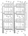
- FIG. 20 is a diagram illustrating the configuration of 8 ⁇ 16 MCS according to the fifth embodiment of the present invention.
- FIG. 20 shows eight input ports In 1 to In 8 , 16 output ports Out 1 to Out 16 , 128 SU 510, input ports In 1 to In 8 , SU 510, and output ports Out 1 to An 8 ⁇ 16 MCS 500 in which an optical waveguide 501 that optically connects between Out 16 , 128 lead lines 515 connected to the SU 510, and four ground lines 517 are formed on a high refractive index waveguide substrate is provided. It is shown.
- the 8 ⁇ 16 MCS 500 includes eight SU columns 540 1 to 540 8 configured by arranging a plurality of SUs 510 of the same number in a column.
- the SU rows 540 1 to 540 8 constitute a U-shaped row by the optical waveguide 501 between the SU rows being folded back by the folded waveguide portion 502.
- four SU rows 550 each formed of two SU rows 540 arranged vertically by introducing a folded waveguide portion are formed.
- Each SU 510 includes a GSW and an MSW provided in a subsequent stage of the GSW.
- the GSW column 520 and the MSW column 530 are respectively configured.
- 1 ⁇ 2 splitters SP each having a demultiplexing ratio set to 1: 1 are provided.
- the 1 ⁇ 2 splitter SP in each SU is an asymmetric splitter, and the demultiplexing ratio is 7: 1, 6: 1, 5: 1, 4: 1 in order from the SU row 540 1 to the SU row 540 7 .
- the present invention can be used in an optical communication system.
Landscapes
- Physics & Mathematics (AREA)
- General Physics & Mathematics (AREA)
- Optics & Photonics (AREA)
- Nonlinear Science (AREA)
- Engineering & Computer Science (AREA)
- Microelectronics & Electronic Packaging (AREA)
- Mathematical Physics (AREA)
- Computer Networks & Wireless Communication (AREA)
- Optical Modulation, Optical Deflection, Nonlinear Optics, Optical Demodulation, Optical Logic Elements (AREA)
- Optical Integrated Circuits (AREA)
- Mechanical Light Control Or Optical Switches (AREA)
- Optical Communication System (AREA)
Abstract
La présente invention concerne un commutateur multidiffusion (MCS) compact ayant la moitié du nombre de lignes principale par rapport à une configuration classique. Selon la présente invention, sont formés sur une carte : M ports d'entrée; N ports de sortie; M × N unités de commutateur optique (SU optiques); un guide d'ondes optique qui connecte optiquement les M ports d'entrée, les M × N SU optiques, et les N ports de sortie; et des lignes principales respectivement connectées aux M × N SU optiques. Un commutateur multidiffusion est configuré de sorte qu'en mettant une SU optique dans un état activé, un signal lumineux est appliqué à l'entrée d'un port d'entrée associé à la SU optique dans l'état activé et est délivré en sortie par un port de sortie associé à la SU optique dans l'état activé. Les M × N SU optiques comprennent au moins un commutateur de grille et un commutateur principal, et les lignes principales connectées aux commutateurs de grille et aux commutateurs principaux dans les SU optiques respectives sont des lignes principales communes.
Priority Applications (3)
| Application Number | Priority Date | Filing Date | Title |
|---|---|---|---|
| US16/982,491 US11287578B2 (en) | 2018-03-29 | 2019-03-26 | Multicast switch |
| CA3094929A CA3094929C (fr) | 2018-03-29 | 2019-03-26 | Commutateur multidiffusion |
| CN201980022617.4A CN111919168B (zh) | 2018-03-29 | 2019-03-26 | 多播开关 |
Applications Claiming Priority (2)
| Application Number | Priority Date | Filing Date | Title |
|---|---|---|---|
| JP2018-065693 | 2018-03-29 | ||
| JP2018065693A JP7015717B2 (ja) | 2018-03-29 | 2018-03-29 | マルチキャストスイッチ |
Publications (1)
| Publication Number | Publication Date |
|---|---|
| WO2019189105A1 true WO2019189105A1 (fr) | 2019-10-03 |
Family
ID=68061675
Family Applications (1)
| Application Number | Title | Priority Date | Filing Date |
|---|---|---|---|
| PCT/JP2019/012731 Ceased WO2019189105A1 (fr) | 2018-03-29 | 2019-03-26 | Commutateur multidiffusion |
Country Status (5)
| Country | Link |
|---|---|
| US (1) | US11287578B2 (fr) |
| JP (1) | JP7015717B2 (fr) |
| CN (1) | CN111919168B (fr) |
| CA (1) | CA3094929C (fr) |
| WO (1) | WO2019189105A1 (fr) |
Families Citing this family (1)
| Publication number | Priority date | Publication date | Assignee | Title |
|---|---|---|---|---|
| JP7015717B2 (ja) * | 2018-03-29 | 2022-02-03 | Nttエレクトロニクス株式会社 | マルチキャストスイッチ |
Citations (5)
| Publication number | Priority date | Publication date | Assignee | Title |
|---|---|---|---|---|
| JPH09297230A (ja) * | 1996-04-30 | 1997-11-18 | Nippon Telegr & Teleph Corp <Ntt> | 導波路型変形2×2光スイッチ及び導波路型マトリクス光スイッチ |
| US5729642A (en) * | 1995-10-02 | 1998-03-17 | The Boeing Company | N×N optical switch array using electro-optic and passive waveguide circuits on planar substrates |
| JP2003005231A (ja) * | 2001-06-26 | 2003-01-08 | Nippon Telegr & Teleph Corp <Ntt> | 光マトリクススイッチ |
| JP2006038897A (ja) * | 2004-07-22 | 2006-02-09 | Nippon Telegr & Teleph Corp <Ntt> | 導波路型光スイッチ単位素子および導波路型マトリクス光スイッチ |
| US20160337731A1 (en) * | 2015-05-13 | 2016-11-17 | Huawei Technologies Co., Ltd. | System and Method for Photonic Switching |
Family Cites Families (6)
| Publication number | Priority date | Publication date | Assignee | Title |
|---|---|---|---|---|
| DE19632282A1 (de) * | 1996-08-09 | 1998-02-19 | Holzer Walter Prof Dr H C Ing | Verfahren und Einrichtung zur Helligkeitssteuerung von Leuchtstofflampen |
| JP3929844B2 (ja) * | 2002-02-19 | 2007-06-13 | 株式会社フジクラ | 光スイッチ、光アドドロップモジュール及び光通信システム |
| CN103370650B (zh) * | 2011-02-15 | 2016-01-06 | 日本电信电话株式会社 | 波导型光开关 |
| US10634851B2 (en) * | 2017-05-17 | 2020-04-28 | Massachusetts Institute Of Technology | Apparatus, systems, and methods for nonblocking optical switching |
| US11194093B2 (en) * | 2018-03-08 | 2021-12-07 | Nippon Telegraph And Telephone Corporation | Optical switch array and multicast switch |
| JP7015717B2 (ja) * | 2018-03-29 | 2022-02-03 | Nttエレクトロニクス株式会社 | マルチキャストスイッチ |
-
2018
- 2018-03-29 JP JP2018065693A patent/JP7015717B2/ja active Active
-
2019
- 2019-03-26 CN CN201980022617.4A patent/CN111919168B/zh active Active
- 2019-03-26 CA CA3094929A patent/CA3094929C/fr active Active
- 2019-03-26 WO PCT/JP2019/012731 patent/WO2019189105A1/fr not_active Ceased
- 2019-03-26 US US16/982,491 patent/US11287578B2/en active Active
Patent Citations (5)
| Publication number | Priority date | Publication date | Assignee | Title |
|---|---|---|---|---|
| US5729642A (en) * | 1995-10-02 | 1998-03-17 | The Boeing Company | N×N optical switch array using electro-optic and passive waveguide circuits on planar substrates |
| JPH09297230A (ja) * | 1996-04-30 | 1997-11-18 | Nippon Telegr & Teleph Corp <Ntt> | 導波路型変形2×2光スイッチ及び導波路型マトリクス光スイッチ |
| JP2003005231A (ja) * | 2001-06-26 | 2003-01-08 | Nippon Telegr & Teleph Corp <Ntt> | 光マトリクススイッチ |
| JP2006038897A (ja) * | 2004-07-22 | 2006-02-09 | Nippon Telegr & Teleph Corp <Ntt> | 導波路型光スイッチ単位素子および導波路型マトリクス光スイッチ |
| US20160337731A1 (en) * | 2015-05-13 | 2016-11-17 | Huawei Technologies Co., Ltd. | System and Method for Photonic Switching |
Also Published As
| Publication number | Publication date |
|---|---|
| JP2019174759A (ja) | 2019-10-10 |
| US11287578B2 (en) | 2022-03-29 |
| US20210018692A1 (en) | 2021-01-21 |
| JP7015717B2 (ja) | 2022-02-03 |
| CA3094929C (fr) | 2023-03-28 |
| CA3094929A1 (fr) | 2019-10-03 |
| CN111919168B (zh) | 2024-07-02 |
| CN111919168A (zh) | 2020-11-10 |
Similar Documents
| Publication | Publication Date | Title |
|---|---|---|
| JP3842511B2 (ja) | 多重ポート・カプラを使用する光学的空間スイッチ | |
| JP5913139B2 (ja) | 導波路型光スイッチ | |
| JP5222083B2 (ja) | 多方路光スイッチ | |
| WO2007123157A1 (fr) | DÉMULTIPLEXEUR optique de groupe de longueurs d'onde, multiplexeur optique de groupe de longueurs d'onde et commutateur de SÉLECTION du LUMIÈRE de groupe de longueurs d'onde | |
| CN110780388A (zh) | 一种波长交换装置及系统 | |
| WO2019189105A1 (fr) | Commutateur multidiffusion | |
| JP4146211B2 (ja) | 光モジュール、およびそれを構成する光スイッチ、並びに光マトリクススイッチ | |
| JP2016212128A (ja) | 光信号処理装置 | |
| JP2010219828A (ja) | 光パスネットワークの光パスクロスコネクト装置および階層化光パスクロスコネクト装置 | |
| JP3444548B2 (ja) | 光スイッチ | |
| US11194093B2 (en) | Optical switch array and multicast switch | |
| JP3727556B2 (ja) | 光マトリクススイッチ | |
| JP6740272B2 (ja) | 光スイッチアレイおよびマルチキャストスイッチ | |
| WO2014049942A1 (fr) | Dispositif de commutation | |
| US9638865B2 (en) | Switch device | |
| JP2774630B2 (ja) | 光信号路の切換装置 | |
| JPH0545931B2 (fr) | ||
| JP2025159756A (ja) | 光スイッチ回路 | |
| JP2020112666A (ja) | 光信号処理装置 | |
| JP6890533B2 (ja) | 光入出力装置 | |
| JP3444543B2 (ja) | 光マトリックススイッチ | |
| JP3444544B2 (ja) | 光マトリックススイッチ | |
| JPH0515119B2 (fr) | ||
| JP2010219827A (ja) | 光パスネットワークの階層化光パスクロスコネクト装置 | |
| JPH0520954B2 (fr) |
Legal Events
| Date | Code | Title | Description |
|---|---|---|---|
| 121 | Ep: the epo has been informed by wipo that ep was designated in this application |
Ref document number: 19774751 Country of ref document: EP Kind code of ref document: A1 |
|
| ENP | Entry into the national phase |
Ref document number: 3094929 Country of ref document: CA |
|
| NENP | Non-entry into the national phase |
Ref country code: DE |
|
| 122 | Ep: pct application non-entry in european phase |
Ref document number: 19774751 Country of ref document: EP Kind code of ref document: A1 |