WO2019205127A1 - Appareil d'affichage, et substrat d'affichage et son procédé de fabrication - Google Patents
Appareil d'affichage, et substrat d'affichage et son procédé de fabrication Download PDFInfo
- Publication number
- WO2019205127A1 WO2019205127A1 PCT/CN2018/085061 CN2018085061W WO2019205127A1 WO 2019205127 A1 WO2019205127 A1 WO 2019205127A1 CN 2018085061 W CN2018085061 W CN 2018085061W WO 2019205127 A1 WO2019205127 A1 WO 2019205127A1
- Authority
- WO
- WIPO (PCT)
- Prior art keywords
- layer
- barrier layer
- encapsulating
- base substrate
- area
- Prior art date
- Legal status (The legal status is an assumption and is not a legal conclusion. Google has not performed a legal analysis and makes no representation as to the accuracy of the status listed.)
- Ceased
Links
Images




Classifications
-
- H—ELECTRICITY
- H10—SEMICONDUCTOR DEVICES; ELECTRIC SOLID-STATE DEVICES NOT OTHERWISE PROVIDED FOR
- H10K—ORGANIC ELECTRIC SOLID-STATE DEVICES
- H10K59/00—Integrated devices, or assemblies of multiple devices, comprising at least one organic light-emitting element covered by group H10K50/00
- H10K59/10—OLED displays
- H10K59/12—Active-matrix OLED [AMOLED] displays
- H10K59/122—Pixel-defining structures or layers, e.g. banks
-
- H—ELECTRICITY
- H10—SEMICONDUCTOR DEVICES; ELECTRIC SOLID-STATE DEVICES NOT OTHERWISE PROVIDED FOR
- H10F—INORGANIC SEMICONDUCTOR DEVICES SENSITIVE TO INFRARED RADIATION, LIGHT, ELECTROMAGNETIC RADIATION OF SHORTER WAVELENGTH OR CORPUSCULAR RADIATION
- H10F19/00—Integrated devices, or assemblies of multiple devices, comprising at least one photovoltaic cell covered by group H10F10/00, e.g. photovoltaic modules
- H10F19/50—Integrated devices comprising at least one photovoltaic cell and other types of semiconductor or solid-state components
-
- H—ELECTRICITY
- H10—SEMICONDUCTOR DEVICES; ELECTRIC SOLID-STATE DEVICES NOT OTHERWISE PROVIDED FOR
- H10K—ORGANIC ELECTRIC SOLID-STATE DEVICES
- H10K50/00—Organic light-emitting devices
- H10K50/80—Constructional details
- H10K50/84—Passivation; Containers; Encapsulations
- H10K50/842—Containers
- H10K50/8426—Peripheral sealing arrangements, e.g. adhesives, sealants
-
- H—ELECTRICITY
- H10—SEMICONDUCTOR DEVICES; ELECTRIC SOLID-STATE DEVICES NOT OTHERWISE PROVIDED FOR
- H10K—ORGANIC ELECTRIC SOLID-STATE DEVICES
- H10K50/00—Organic light-emitting devices
- H10K50/80—Constructional details
- H10K50/84—Passivation; Containers; Encapsulations
- H10K50/844—Encapsulations
- H10K50/8445—Encapsulations multilayered coatings having a repetitive structure, e.g. having multiple organic-inorganic bilayers
-
- H—ELECTRICITY
- H10—SEMICONDUCTOR DEVICES; ELECTRIC SOLID-STATE DEVICES NOT OTHERWISE PROVIDED FOR
- H10K—ORGANIC ELECTRIC SOLID-STATE DEVICES
- H10K59/00—Integrated devices, or assemblies of multiple devices, comprising at least one organic light-emitting element covered by group H10K50/00
- H10K59/10—OLED displays
- H10K59/12—Active-matrix OLED [AMOLED] displays
- H10K59/1201—Manufacture or treatment
-
- H—ELECTRICITY
- H10—SEMICONDUCTOR DEVICES; ELECTRIC SOLID-STATE DEVICES NOT OTHERWISE PROVIDED FOR
- H10K—ORGANIC ELECTRIC SOLID-STATE DEVICES
- H10K59/00—Integrated devices, or assemblies of multiple devices, comprising at least one organic light-emitting element covered by group H10K50/00
- H10K59/80—Constructional details
- H10K59/87—Passivation; Containers; Encapsulations
- H10K59/873—Encapsulations
- H10K59/8731—Encapsulations multilayered coatings having a repetitive structure, e.g. having multiple organic-inorganic bilayers
-
- H—ELECTRICITY
- H10—SEMICONDUCTOR DEVICES; ELECTRIC SOLID-STATE DEVICES NOT OTHERWISE PROVIDED FOR
- H10K—ORGANIC ELECTRIC SOLID-STATE DEVICES
- H10K71/00—Manufacture or treatment specially adapted for the organic devices covered by this subclass
-
- H—ELECTRICITY
- H10—SEMICONDUCTOR DEVICES; ELECTRIC SOLID-STATE DEVICES NOT OTHERWISE PROVIDED FOR
- H10K—ORGANIC ELECTRIC SOLID-STATE DEVICES
- H10K71/00—Manufacture or treatment specially adapted for the organic devices covered by this subclass
- H10K71/40—Thermal treatment, e.g. annealing in the presence of a solvent vapour
Definitions
- the present invention relates to display technology, more particularly, to a display substrate having a display area and a peripheral area, a display apparatus, and a method of fabricating a display substrate.
- OLED display apparatuses are self-emissive devices, and do not require backlights. OLED display apparatuses also provide more vivid colors and a larger color gamut as compared to the conventional liquid crystal display (LCD) apparatuses. Further, OLED display apparatuses can be made more flexible, thinner, and lighter than a typical LCD.
- An OLED display apparatus typically includes an anode, an organic layer including a light emitting layer, and a cathode. OLEDs can be either a bottom-emission type OLED or a top-emission type OLED.
- the present invention provides a display substrate having a display area and a peripheral area, comprising a base substrate; a plurality of light emitting elements on the base substrate and in the display area; an encapsulating layer on a side of the plurality of light emitting elements distal to the base substrate to encapsulate the plurality of light emitting elements; and a first barrier layer on the base substrate and in the peripheral area and forming a first enclosure substantially surrounding a first area; wherein the first barrier layer comprises an up-conversion material configured to convert an incident light into an ultraviolet light; and wherein the encapsulating layer comprises a first organic encapsulating sub-layer on the base substrate.
- the display substrate further comprises a first inorganic encapsulating sub-layer encapsulating the plurality of light emitting elements and the first barrier layer; wherein the first organic encapsulating sub-layer is substantially enclosed inside the first area and is on a side of the first inorganic encapsulating sub-layer distal to the base substrate.
- the display substrate further comprises a second barrier layer on the base substrate and in the peripheral area and forming a second enclosure substantially surrounding a second area, the second area being larger than the first area; wherein the first inorganic encapsulating sub-layer encapsulates the plurality of light emitting elements, the first barrier layer, and the second barrier layer; and the first inorganic encapsulating sub-layer is in contact with the base substrate in an area between the first barrier layer and the second barrier layer.
- the first organic encapsulating sub-layer is substantially enclosed inside the second area.
- the second barrier layer comprises the up-conversion material configured to convert the incident light into the ultraviolet light.
- the second barrier layer has a height relative to the base substrate greater than a height relative to the base substrate of the first barrier layer.
- first barrier layer and the second barrier layer are spaced apart from each other by a distance in a range of approximately 0.5 mm to approximately 2 mm; and each of the first barrier layer and the second barrier layer has a lateral thickness in a range of approximately 10 ⁇ m to approximately 20 ⁇ m.
- the encapsulating layer further comprises a second inorganic encapsulating sub-layer on a side of the first organic encapsulating sub-layer distal to the base substrate, encapsulating the plurality of light emitting elements, the first barrier layer, the second barrier layer, the first inorganic encapsulating sub-layer, and the first organic encapsulating sub-layer.
- the encapsulating layer further comprises a second organic encapsulating sub-layer on a side of the second inorganic encapsulating sub-layer distal to the base substrate, and substantially enclosed inside the second area.
- the encapsulating layer further comprises a third inorganic encapsulating sub-layer on a side of the second organic encapsulating sub-layer distal to the base substrate.
- the display substrate further comprises a third barrier layer on the base substrate and in the peripheral area and forming a third enclosure substantially surrounding a third area, the third area being larger than the second area; wherein the first inorganic encapsulating sub-layer is on a side of the first barrier layer, the second barrier layer, and the third barrier layer distal to the base substrate, encapsulating the plurality of light emitting elements, the first barrier layer, the second barrier layer, and the third barrier layer; the first inorganic encapsulating sub-layer is in contact with the base substrate in an area between the second barrier layer and the third barrier layer; and the second inorganic encapsulating sub-layer is on a side of the first inorganic encapsulating sub-layer and the first organic encapsulating sub-layer distal to the base substrate, encapsulating the plurality of light emitting elements, the first barrier layer, the second barrier layer, the third barrier layer, the first inorganic encapsulating sub-layer, and the first organic encapsulating sub-layer.
- the encapsulating layer further comprises a second organic encapsulating sub-layer on a side of the second inorganic encapsulating sub-layer distal to the base substrate, and substantially enclosed inside the third area.
- the third barrier layer comprises the up-conversion material configured to convert the incident light into the ultraviolet light.
- the second barrier layer has a height relative to the base substrate greater than a height relative to the base substrate of the first barrier layer; and the third barrier layer has a height relative to the base substrate greater than the height relative to the base substrate of the second barrier layer.
- the encapsulating layer further comprises a third inorganic encapsulating sub-layer encapsulating the plurality of light emitting elements, the first barrier layer, the second barrier layer, the third barrier layer, the first inorganic encapsulating sub-layer, the second inorganic encapsulating sub-layer, the first organic encapsulating sub-layer, and the second organic encapsulating sub-layer.
- the present invention provides a display apparatus comprising the display substrate described herein.
- the present invention provides a method of fabricating a display substrate having a display area and a peripheral area, comprising forming a plurality of light emitting elements on a base substrate and in the display area; forming an encapsulating layer on a side of the plurality of light emitting elements distal to the base substrate to encapsulate the plurality of light emitting elements; and forming a first barrier layer on the base substrate and in the peripheral area, the first barrier layer forming a first enclosure substantially surrounding a first area; wherein the first barrier layer is formed using a material comprising an up-conversion material configured to convert an incident light into an ultraviolet light; and wherein forming the encapsulating layer comprises forming a first organic encapsulating sub-layer on the base substrate.
- forming the first organic encapsulating sub-layer comprises forming a first organic material layer substantially enclosed inside the first area; subsequent to forming the first organic material layer, irradiating the first barrier layer by the incident light, the first barrier layer converting the incident light into the ultraviolet light; and curing a peripheral portion of the first organic material layer by the ultraviolet light converted by the first barrier layer, thereby stabilizing the peripheral portion of the first organic material layer.
- the method further comprises forming a first inorganic encapsulating sub-layer encapsulating the plurality of light emitting elements and the first barrier layer; wherein the first organic encapsulating sub-layer is formed on a side of the first inorganic encapsulating sub-layer distal to the base substrate.
- the method further comprises forming a second barrier layer on the base substrate and in the peripheral area, the second barrier layer forming a second enclosure substantially surrounding a second area, the second area being larger than the first area; wherein the first inorganic encapsulating sub-layer is formed to encapsulate the plurality of light emitting elements, the first barrier layer, and the second barrier layer; and the first inorganic encapsulating sub-layer is formed to be in contact with the base substrate in an area between the first barrier layer and the second barrier layer.
- the first organic encapsulating sub-layer is formed to be substantially enclosed inside the second area; wherein forming the first organic encapsulating sub-layer comprises forming a first organic material layer substantially enclosed inside the second area; subsequent to forming the first organic material layer, irradiating the first barrier layer by the incident light, the first barrier layer converting the incident light into the ultraviolet light; and curing a peripheral portion of the first organic material layer by the ultraviolet light converted by the first barrier layer, thereby stabilizing the peripheral portion of the first organic material layer.
- the second barrier layer is formed using a material comprising the up-conversion material configured to convert the incident light into the ultraviolet light; and wherein forming the encapsulating layer further comprises forming a first organic encapsulating sub-layer on a side of the first inorganic encapsulating sub-layer distal to the base substrate, and substantially enclosed inside the second area; wherein forming the first organic encapsulating sub-layer comprises forming a first organic material layer substantially enclosed inside the second area; subsequent to forming the first organic material layer, irradiating the first barrier layer and the second barrier layer by the incident light, the first barrier layer and the second barrier layer converting the incident light into the ultraviolet light; and curing a peripheral portion of the first organic material layer by the ultraviolet light converted by the first barrier layer and the second barrier layer, thereby stabilizing the peripheral portion of the first organic material layer.
- the second barrier layer is formed to have a height relative to the base substrate greater than a height relative to the base substrate of the first barrier layer.
- first barrier layer and the second barrier layer are formed to be spaced apart from each other by a distance in a range of approximately 0.5 mm to approximately 2 mm; and each of the first barrier layer and the second barrier layer is formed to have a lateral thickness in a range of approximately 10 ⁇ m to approximately 20 ⁇ m.
- forming the encapsulating layer further comprises forming a second inorganic encapsulating sub-layer on a side of the first organic encapsulating sub-layer distal to the base substrate, encapsulating the plurality of light emitting elements, the first barrier layer, the second barrier layer, the first inorganic encapsulating sub-layer, and the first organic encapsulating sub-layer.
- forming the encapsulating layer further comprises forming a second organic encapsulating sub-layer on a side of the second inorganic encapsulating sub-layer distal to the base substrate, and the second organic encapsulating sub-layer is formed to be substantially enclosed inside the second area.
- forming the encapsulating layer further comprises forming a third inorganic encapsulating sub-layer on a side of the second organic encapsulating sub-layer distal to the base substrate.
- the method further comprises forming a third barrier layer on the base substrate and in the peripheral area, the third barrier layer forming a third enclosure substantially surrounding a third area, the third area being larger than the second area; wherein the first inorganic encapsulating sub-layer is formed on a side of the first barrier layer, the second barrier layer, and the third barrier layer distal to the base substrate, encapsulating the plurality of light emitting elements, the first barrier layer, the second barrier layer, and the third barrier layer; the first inorganic encapsulating sub-layer is formed to be in contact with the base substrate in an area between the second barrier layer and the third barrier layer; and the second inorganic encapsulating sub-layer is formed on a side of the first inorganic encapsulating sub-layer and the first organic encapsulating sub-layer distal to the base substrate, encapsulating the plurality of light emitting elements, the first barrier layer, the second barrier layer, the third barrier layer, the first inorganic encapsulating sub-layer, and the first organic
- forming the encapsulating layer further comprises forming a second organic encapsulating sub-layer on a side of the second inorganic encapsulating sub-layer distal to the base substrate, and the second organic encapsulating sub-layer is formed to be substantially enclosed inside the third area; wherein forming the second organic encapsulating sub-layer comprises forming a second organic material layer substantially enclosed inside the third area; subsequent to forming the second organic material layer, irradiating the second barrier layer and the third barrier layer by the incident light, the second barrier layer and the third barrier layer converting the incident light into the ultraviolet light; and curing a peripheral portion of the second organic material layer by the ultraviolet light converted by the second barrier layer and the third barrier layer, thereby stabilizing the peripheral portion of the second organic material layer.
- the third barrier layer is formed using a material comprising the up-conversion material configured to convert the incident light into the ultraviolet light.
- the second barrier layer is formed to have a height relative to the base substrate greater than a height relative to the base substrate of the first barrier layer; and the third barrier layer is formed to have a height relative to the base substrate greater than the height relative to the base substrate of the second barrier layer.
- forming the encapsulating layer further comprises forming a third inorganic encapsulating sub-layer encapsulating the plurality of light emitting elements, the first barrier layer, the second barrier layer, the third barrier layer, the first inorganic encapsulating sub-layer, the second inorganic encapsulating sub-layer, the first organic encapsulating sub-layer, and the second organic encapsulating sub-layer.
- FIG. 1 is a schematic diagram illustrating the structure of a display substrate in some embodiments according to the present disclosure.
- FIG. 2 is a schematic diagram illustrating the structure of a display substrate in some embodiments according to the present disclosure.
- FIG. 3 is a schematic diagram illustrating the structure of a display substrate in some embodiments according to the present disclosure.
- FIG. 4 is a schematic diagram illustrating the structure of a display substrate in some embodiments according to the present disclosure.
- FIG. 5 is a schematic diagram illustrating the structure of a display substrate in some embodiments according to the present disclosure.
- FIGs. 6A to 6D illustrate a process of fabricating a display substrate in some embodiments according to the present disclosure.
- FIGs. 7A to 7G illustrate a process of fabricating a display substrate in some embodiments according to the present disclosure.
- FIGs. 8A to 8D illustrate a process of fabricating a display substrate in some embodiments according to the present disclosure.
- FIGs. 9A to 9G illustrate a process of fabricating a display substrate in some embodiments according to the present disclosure.
- an encapsulating layer for a display substrate e.g., an organic light emitting diode display substrate
- multiple sub-layers including one or more inorganic sub- layers and one or more organic sub-layers are formed on the display substrate.
- the organic sub-layers may be formed by printing (e.g., ink-jet printing) an organic ink onto the display substrate, and curing the organic ink to form the organic sub-layer.
- the organic ink is allowed to be substantially leveled before it is cured, e.g., by an ultraviolet light.
- the display substrate includes one or more barrier layer to hold the organic ink in a defined region before it is cured. However, often the organic ink climbs over the barrier layer.
- the organic ink When the organic ink is cured to form an organic sub-layer, and an inorganic sub-layer is subsequently formed on top of the organic sub-layer, the organic sub-layer extends outside the inorganic sub-layer. Because the organic sub-layer is not completely encapsulated by the inorganic sub-layer, the display substrate has an inferior oxygen and moisture resistance.
- the present disclosure provides, inter alia, a display substrate having a display area and a peripheral area, a display apparatus, and a method of fabricating a display substrate that substantially obviate one or more of the problems due to limitations and disadvantages of the related art.
- the present disclosure provides a display substrate having a display area and a peripheral area.
- the display substrate includes a base substrate; a plurality of light emitting elements on the base substrate and in the display area; an encapsulating layer on a side of the plurality of light emitting elements distal to the base substrate to encapsulate the plurality of light emitting elements; and a first barrier layer on the base substrate and in the peripheral area and forming a first enclosure substantially surrounding a first area.
- the first barrier layer includes an up-conversion material configured to convert an incident light into an ultraviolet light.
- the up-conversion material is capable of converting an infrared light into an ultraviolet light.
- the up-conversion material is capable of converting a visible light into an ultraviolet light.
- the encapsulating layer includes a first organic encapsulating sub-layer on a side of the first barrier layer distal to the base substrate.
- the term “display area” refers to an area of a display substrate (e.g., an opposing substrate or an array substrate) in a display panel where image is actually displayed.
- the display area may include both a subpixel region and an inter-subpixel region.
- a subpixel region refers to a light emission region of a subpixel, such as a region corresponding to a pixel electrode in a liquid crystal display or a region corresponding to a light emissive layer in an organic light emitting diode display panel.
- An inter-subpixel region refers to a region between adjacent subpixel regions, such as a region corresponding to a black matrix in a liquid crystal display or a region corresponding a pixel definition layer in an organic light emitting diode display panel.
- the inter-subpixel region is a region between adjacent subpixel regions in a same pixel.
- the inter-subpixel region is a region between two adjacent subpixel regions from two adjacent pixels.
- peripheral area refers to an area of a display substrate (e.g., an opposing substrate or an array substrate) in a display panel where various circuits and wires are provided to transmit signals to the display substrate.
- a display substrate e.g., an opposing substrate or an array substrate
- non-transparent or opaque components of the display apparatus e.g., battery, printed circuit board, metal frame
- the peripheral area rather than in the display areas.
- substantially surrounding refers to surrounding at least 50%(e.g., at least 60%, at least 70%, at least 80%, at least 90%, at least 95%, at least 99%, and 100%) of a perimeter of an area.
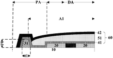
- FIG. 1 is a schematic diagram illustrating the structure of a display substrate in some embodiments according to the present disclosure.
- the display substrate in some embodiments has a display area DA and a peripheral area PA.
- the display substrate includes a base substrate 10; a plurality of light emitting elements 20 on the base substrate 10 and in the display area DA; an encapsulating layer 60 on a side of the plurality of light emitting elements 20 distal to the base substrate 10 to encapsulate the plurality of light emitting elements 20; and a first barrier layer 31 on the base substrate 10 and in the peripheral area PA and forming a first enclosure substantially surrounding a first area A1.
- the first barrier layer 31 includes an up-conversion material configured to convert an incident light into an ultraviolet light.
- the up-conversion material is capable of converting an infrared light into an ultraviolet light.
- the up-conversion material is capable of converting a visible light into an ultraviolet light.
- a barrier material may be deposited on the substrate by a plasma-enhanced chemical vapor deposition (PECVD) process.
- PECVD plasma-enhanced chemical vapor deposition
- appropriate barrier materials include a polymer material containing one or more up-conversion materials.
- appropriate polymer materials include resins and photoresist materials.
- appropriate up-conversion materials includes a compound having one or more rare earth elements, e.g., an oxide of one or more rare earth elements, a halide (e.g., a fluoride) of one or more rare earth elements, an oxyfluoride of one or more rare earth elements, a sulfide of one or more rare earth elements, and any combination thereof.
- the first barrier layer 31 is made of a photoresist resin including 10%weight/weight ⁇ -NaYF_4: Yb ⁇ (3+) , Tm ⁇ (3+) /CdSe nanocrystals.
- the first barrier layer 31 has a lateral thickness t1 in a range of approximately 5 ⁇ m to approximately 50 ⁇ m, e.g., approximately 5 ⁇ m to approximately 10 ⁇ m, approximately 10 ⁇ m to approximately 15 ⁇ m, approximately 15 ⁇ m to approximately 20 ⁇ m, approximately 20 ⁇ m to approximately 25 ⁇ m, approximately 25 ⁇ m to approximately 30 ⁇ m, approximately 30 ⁇ m to approximately 35 ⁇ m, approximately 35 ⁇ m to approximately 40 ⁇ m, approximately 40 ⁇ m to approximately 45 ⁇ m, and approximately 45 ⁇ m to approximately 50 ⁇ m.
- a lateral thickness t1 in a range of approximately 5 ⁇ m to approximately 50 ⁇ m, e.g., approximately 5 ⁇ m to approximately 10 ⁇ m, approximately 10 ⁇ m to approximately 15 ⁇ m, approximately 15 ⁇ m to approximately 20 ⁇ m, approximately 20 ⁇ m to approximately 25 ⁇ m, approximately 25 ⁇ m to approximately 30 ⁇ m, approximately 30 ⁇ m to approximately 35 ⁇ m, approximately 35
- the first barrier layer 31 may have a cross-section of any appropriate shapes.
- appropriate shapes of the cross-section of the first barrier layer 31 includes a circular shape, a trapezoidal shape, an inverted trapezoidal shape, an elliptical shape, a square shape, and a triangular shape.
- the first barrier layer 31 has a height h1 relative to the base substrate 10 in a range of approximately 0.5 ⁇ m to approximately 5 ⁇ m, e.g., approximately 0.5 ⁇ m to approximately 1 ⁇ m, approximately 1 ⁇ m to approximately 1.5 ⁇ m, approximately 1.5 ⁇ m to approximately 2 ⁇ m, approximately 2 ⁇ m to approximately 2.5 ⁇ m, approximately 2.5 ⁇ m to approximately 3 ⁇ m, approximately 3 ⁇ m to approximately 3.5 ⁇ m, approximately 3.5 ⁇ m to approximately 4 ⁇ m, approximately 4 ⁇ m to approximately 4.5 ⁇ m, and approximately 4.5 ⁇ m to approximately 5 ⁇ m.
- the first barrier layer 31 has a height h1 relative to the base substrate 10 of approximately 2 ⁇ m.
- the display substrate further includes a second barrier layer 32 on the base substrate 10 and in the peripheral area PA and forming a second enclosure substantially surrounding a second area A2, the second area A2 being larger than the first area A1.
- a barrier material may be deposited on the substrate by a plasma-enhanced chemical vapor deposition (PECVD) process.
- PECVD plasma-enhanced chemical vapor deposition
- appropriate barrier materials include a polymer material such as various resins and photoresist materials.
- the second barrier layer 32 also includes an up-conversion material configured to convert the incident light into the ultraviolet light.
- up-conversion materials includes a compound having one or more rare earth elements, e.g., an oxide of one or more rare earth elements, a halide (e.g., a fluoride) of one or more rare earth elements, an oxyfluoride of one or more rare earth elements, a sulfide of one or more rare earth elements, and any combination thereof.
- rare earth elements for making the up-conversion materials include Lanthanum, Cerium, Praseodymium, Neodymium, Promethium, Samarium, Europium, Gadolinium, Terbium, Dysprosium, Holmium, Erbium, Thulium, Ytterbium, Lutetium, Scandium, and Yttrium.
- the second barrier layer 32 does not include an up-conversion material.
- the second barrier layer 32 has a lateral thickness t2 in a range of approximately 5 ⁇ m to approximately 50 ⁇ m, e.g., approximately 5 ⁇ m to approximately 10 ⁇ m, approximately 10 ⁇ m to approximately 15 ⁇ m, approximately 15 ⁇ m to approximately 20 ⁇ m, approximately 20 ⁇ m to approximately 25 ⁇ m, approximately 25 ⁇ m to approximately 30 ⁇ m, approximately 30 ⁇ m to approximately 35 ⁇ m, approximately 35 ⁇ m to approximately 40 ⁇ m, approximately 40 ⁇ m to approximately 45 ⁇ m, and approximately 45 ⁇ m to approximately 50 ⁇ m.
- the second barrier layer 32 may have a cross-section of any appropriate shapes.
- appropriate shapes of the cross-section of the second barrier layer 32 includes a circular shape, a trapezoidal shape, an inverted trapezoidal shape, an elliptical shape, a square shape, and a triangular shape.
- the second barrier layer 32 has a height h2 relative to the base substrate 10 in a range of approximately 0.5 ⁇ m to approximately 5 ⁇ m, e.g., approximately 0.5 ⁇ m to approximately 1 ⁇ m, approximately 1 ⁇ m to approximately 1.5 ⁇ m, approximately 1.5 ⁇ m to approximately 2 ⁇ m, approximately 2 ⁇ m to approximately 2.5 ⁇ m, approximately 2.5 ⁇ m to approximately 3 ⁇ m, approximately 3 ⁇ m to approximately 3.5 ⁇ m, approximately 3.5 ⁇ m to approximately 4 ⁇ m, approximately 4 ⁇ m to approximately 4.5 ⁇ m, and approximately 4.5 ⁇ m to approximately 5 ⁇ m.
- the second barrier layer 32 has a height h2 relative to the base substrate 10 of approximately 3 ⁇ m.
- the second barrier layer 32 has a height h2 relative to the base substrate 10 greater than a height h1 relative to the base substrate 10 of the first barrier layer 31.
- the height h2 relative to the base substrate 10 of the second barrier layer 32 is approximately twice the height h1 relative to the base substrate 10 of the first barrier layer 31.
- the first barrier layer 31 has a height h1 relative to the base substrate 10 in a range of approximately 1 ⁇ m to approximately 2 ⁇ m
- the second barrier layer 32 has a height h2 relative to the base substrate 10 in a range of approximately 3 ⁇ m to approximately 4 ⁇ m.
- the first barrier layer 31 and the second barrier layer 32 are spaced apart from each other by a distance in a range of approximately 0.5 mm to approximately 5 mm, e.g., approximately 0.5 mm to approximately 1 mm, approximately 1 mm to approximately 1.5 mm, approximately 1.5 mm to approximately 2 mm, approximately 2 mm to approximately 2.5 mm, approximately 2.5 mm to approximately 3 mm, approximately 3 mm to approximately 3.5 mm, approximately 3.5 mm to approximately 4 mm, approximately 4 mm to approximately 4.5 mm, and approximately 4.5 mm to approximately 5 mm.
- the first barrier layer 31 and the second barrier layer 32 are spaced apart from each other by a distance of approximately 1 mm.
- the encapsulating layer 60 includes a first inorganic encapsulating sub-layer 41 encapsulating the plurality of light emitting elements 20, the first barrier layer 31, and the second barrier layer 32.
- the first inorganic encapsulating sub-layer 41 is in contact with the base substrate 10 in an area between the first barrier layer 31 and the second barrier layer 32.
- an inorganic encapsulating material may be deposited on the substrate by a plasma-enhanced chemical vapor deposition (PECVD) process or an atomic layer deposition process.
- PECVD plasma-enhanced chemical vapor deposition
- atomic layer deposition process examples include, but are not limited to, silicon oxide (SiO y ) , silicon nitride (SiN y , e.g., Si 3 N 4 ) , silicon oxynitride (SiO x N y ) , silicon carbide (SiC) , aluminum oxide, zinc sulfide, and zinc oxide.
- the first inorganic encapsulating sub-layer 41 has a thickness in a range of approximately 0.05 ⁇ m to approximately 2.5 ⁇ m.
- the first inorganic encapsulating sub-layer 41 is made of a substantially transparent material.
- substantially transparent means at least 50 percent (e.g., at least 60 percent, at least 70 percent, at least 80 percent, at least 90 percent, and at least 95 percent) of light in the visible wavelength range transmitted therethrough.
- the first inorganic encapsulating sub-layer 41 includes silicon nitride and have a thickness of approximately 1 ⁇ m, and is formed using a chemical vapor deposition process.
- the encapsulating layer 60 further includes a first organic encapsulating sub-layer 51 on a side of the first inorganic encapsulating sub-layer 41 distal to the base substrate 10, and substantially enclosed inside the second area A2 by the second barrier layer 32.
- the first organic encapsulating sub-layer 51 may be made from a polymerizable monomer (e.g., > 95%v/v) .
- the first organic encapsulating sub-layer 51 is made by curing the polymerizable monomer, e.g., using a UV light.
- the first organic encapsulating sub-layer 51 is made by curing a mixture including the polymerizable monomer, a photo-initiator, a reactive diluent, and one or more additional agents.
- the first organic encapsulating sub-layer 51 has a thickness in a range of approximately 10 ⁇ m to approximately 20 ⁇ m.
- the encapsulating layer 60 in some embodiments further includes a second inorganic encapsulating sub-layer 42 encapsulating the plurality of light emitting elements 20, the first barrier layer 31, the second barrier layer 32, and the first organic encapsulating sub-layer 51.
- an inorganic encapsulating material may be deposited on the substrate by a plasma-enhanced chemical vapor deposition (PECVD) process or an atomic layer deposition process.
- PECVD plasma-enhanced chemical vapor deposition
- atomic layer deposition process examples include, but are not limited to, silicon oxide (SiO y ) , silicon nitride (SiN y , e.g., Si 3 N 4 ) , silicon oxynitride (SiO x N y ) , silicon carbide (SiC) , aluminum oxide, zinc sulfide, and zinc oxide.
- the second inorganic encapsulating sub-layer 42 has a thickness in a range of approximately 0.05 ⁇ m to approximately 2.5 ⁇ m.
- the second inorganic encapsulating sub-layer 42 is made of a substantially transparent material.
- the second inorganic encapsulating sub- layer 42 includes aluminum oxide and have a thickness of approximately 0.05 ⁇ m, and is formed using an atomic layer deposition process.
- FIG. 2 is a schematic diagram illustrating the structure of a display substrate in some embodiments according to the present disclosure.
- the display substrate in some embodiments further includes a third barrier layer 33 on the base substrate 10 and in the peripheral area PA and forming a third enclosure substantially surrounding a third area A3, the third area A3 being larger than the second area A2.
- a first organic encapsulating sub-layer 51 is on a side of the first inorganic encapsulating sub-layer 41 distal to the base substrate 10, and substantially enclosed inside the second area A2 by the second barrier layer 32.
- the first inorganic encapsulating sub-layer 41 is on a side of the first barrier layer 31, the second barrier layer 32, and the third barrier layer 33 distal to the base substrate 10, encapsulating the plurality of light emitting elements 20, the first barrier layer 31, the second barrier layer 32, and the third barrier layer 33.
- the first inorganic encapsulating sub-layer 41 is in contact with the base substrate 10 in an area between the first barrier layer 31 and the second barrier layer 32, and in an area between the second barrier layer 32 and the third barrier layer 33.
- the second inorganic encapsulating sub-layer 42 is on a side of the first inorganic encapsulating sub-layer 41 and the first organic encapsulating sub-layer 51 distal to the base substrate 10.
- the second inorganic encapsulating sub-layer 42 encapsulates the plurality of light emitting elements 20, the first barrier layer 31, the second barrier layer 32, the third barrier layer 33, the first inorganic encapsulating sub-layer 41, and the first organic encapsulating sub-layer 51.
- a barrier material may be deposited on the substrate by a plasma-enhanced chemical vapor deposition (PECVD) process.
- PECVD plasma-enhanced chemical vapor deposition
- appropriate barrier materials include a polymer material such as various resins and photoresist materials.
- the third barrier layer 33 also includes an up-conversion material configured to convert the incident light into the ultraviolet light.
- an up-conversion material includes a compound having one or more rare earth elements, e.g., an oxide of one or more rare earth elements, a halide (e.g., a fluoride) of one or more rare earth elements, an oxyfluoride of one or more rare earth elements, a sulfide of one or more rare earth elements, and any combination thereof.
- rare earth elements for making the up-conversion materials include Lanthanum, Cerium, Praseodymium, Neodymium, Promethium, Samarium, Europium, Gadolinium, Terbium, Dysprosium, Holmium, Erbium, Thulium, Ytterbium, Lutetium, Scandium, and Yttrium.
- the third barrier layer 33 does not include an up-conversion material.
- the third barrier layer 33 has a lateral thickness t3 in a range of approximately 5 ⁇ m to approximately 50 ⁇ m, e.g., approximately 5 ⁇ m to approximately 10 ⁇ m, approximately 10 ⁇ m to approximately 15 ⁇ m, approximately 15 ⁇ m to approximately 20 ⁇ m, approximately 20 ⁇ m to approximately 25 ⁇ m, approximately 25 ⁇ m to approximately 30 ⁇ m, approximately 30 ⁇ m to approximately 35 ⁇ m, approximately 35 ⁇ m to approximately 40 ⁇ m, approximately 40 ⁇ m to approximately 45 ⁇ m, and approximately 45 ⁇ m to approximately 50 ⁇ m.
- the third barrier layer 33 may have a cross-section of any appropriate shapes.
- appropriate shapes of the cross-section of the third barrier layer 33 includes a circular shape, a trapezoidal shape, an inverted trapezoidal shape, an elliptical shape, a square shape, and a triangular shape.
- the third barrier layer 33 has a height h3 relative to the base substrate 10 in a range of approximately 0.5 ⁇ m to approximately 5 ⁇ m, e.g., approximately 0.5 ⁇ m to approximately 1 ⁇ m, approximately 1 ⁇ m to approximately 1.5 ⁇ m, approximately 1.5 ⁇ m to approximately 2 ⁇ m, approximately 2 ⁇ m to approximately 2.5 ⁇ m, approximately 2.5 ⁇ m to approximately 3 ⁇ m, approximately 3 ⁇ m to approximately 3.5 ⁇ m, approximately 3.5 ⁇ m to approximately 4 ⁇ m, approximately 4 ⁇ m to approximately 4.5 ⁇ m, and approximately 4.5 ⁇ m to approximately 5 ⁇ m.
- the third barrier layer 33 has a height h3 relative to the base substrate 10 of approximately 4 ⁇ m.
- the third barrier layer 33 has a height h3 relative to the base substrate 10 greater than a height h2 relative to the base substrate 10 of the second barrier layer 32.
- the height h3 relative to the base substrate 10 of the third barrier layer 33 is approximately twice the height h2 relative to the base substrate 10 of the second barrier layer 32.
- the second barrier layer 32 has a height h2 relative to the base substrate 10 in a range of approximately 3 ⁇ m to approximately 4 ⁇ m
- the third barrier layer 33 has a height h3 relative to the base substrate 10 in a range of approximately 4 ⁇ m to approximately 6 ⁇ m.
- the second barrier layer 32 and the third barrier layer 33 are spaced apart from each other by a distance in a range of approximately 0.5 mm to approximately 5 mm, e.g., approximately 0.5 mm to approximately 1 mm, approximately 1 mm to approximately 1.5 mm, approximately 1.5 mm to approximately 2 mm, approximately 2 mm to approximately 2.5 mm, approximately 2.5 mm to approximately 3 mm, approximately 3 mm to approximately 3.5 mm, approximately 3.5 mm to approximately 4 mm, approximately 4 mm to approximately 4.5 mm, and approximately 4.5 mm to approximately 5 mm.
- the second barrier layer 32 and the third barrier layer 33 are spaced apart from each other by a distance of approximately 1 mm.
- the encapsulating layer 60 further comprises a second organic encapsulating sub-layer 52 on a side of the second inorganic encapsulating sub-layer 42 distal to the base substrate 10, and substantially enclosed inside the third area A3.
- the second organic encapsulating sub-layer 52 may be made from a polymerizable monomer (e.g., > 95%v/v) .
- the second organic encapsulating sub-layer 52 is made by curing the polymerizable monomer, e.g., using a UV light.
- the second organic encapsulating sub-layer 52 is made by curing a mixture including the polymerizable monomer, a photo-initiator, a reactive diluent, and one or more additional agents.
- the second organic encapsulating sub-layer 52 has a thickness in a range of approximately 10 ⁇ m to approximately 20 ⁇ m.
- the encapsulating layer 60 in some embodiments further includes a third inorganic encapsulating sub-layer 43 encapsulating the plurality of light emitting elements 20, the first barrier layer 31, the second barrier layer 32, the third barrier layer 33, the first inorganic encapsulating sub-layer 41, the second inorganic encapsulating sub-layer 42, the first organic encapsulating sub-layer 51, and the second organic encapsulating sub-layer 52.
- an inorganic encapsulating material may be deposited on the substrate by a plasma- enhanced chemical vapor deposition (PECVD) process or an atomic layer deposition process.
- PECVD plasma- enhanced chemical vapor deposition
- appropriate inorganic encapsulating materials include, but are not limited to, silicon oxide (SiO y ) , silicon nitride (SiN y , e.g., Si 3 N 4 ) , silicon oxynitride (SiO x N y ) , silicon carbide (SiC) , aluminum oxide, zinc sulfide, and zinc oxide.
- the third inorganic encapsulating sub-layer 43 has a thickness in a range of approximately 0.05 ⁇ m to approximately 2.5 ⁇ m.
- the third inorganic encapsulating sub-layer 43 is made of a substantially transparent material.
- the third inorganic encapsulating sub-layer 43 includes silicon oxide and have a thickness of approximately 1 ⁇ m, and is formed using a chemical vapor deposition process.
- the display substrate includes additional barrier layer (s) , additional inorganic encapsulating sub-layer (s) , and/or additional organic encapsulating sub-layer (s) .
- FIG. 3 is a schematic diagram illustrating the structure of a display substrate in some embodiments according to the present disclosure.
- the display substrate in some embodiments includes a base substrate 10; a plurality of light emitting elements 20 on the base substrate 10 and in the display area DA; an encapsulating layer 60 on a side of the plurality of light emitting elements 20 distal to the base substrate 10 to encapsulate the plurality of light emitting elements 20; and a first barrier layer 31 on the base substrate 10 and in the peripheral area PA and forming a first enclosure substantially surrounding a first area A1.
- the first barrier layer 31 includes an up-conversion material configured to convert an incident light into an ultraviolet light.
- the up-conversion material is capable of converting an infrared light into an ultraviolet light.
- the up-conversion material is capable of converting a visible light into an ultraviolet light.
- the encapsulating layer 60 includes a first inorganic encapsulating sub-layer 41 encapsulating the plurality of light emitting elements 20 and the first barrier layer 31; a first organic encapsulating sub-layer 51 on a side of the first inorganic encapsulating sub-layer 41 distal to the base substrate 10; and a second inorganic encapsulating sub-layer 42 on a side of the first organic encapsulating sub-layer 51 distal to the base substrate 10 and encapsulating the plurality of light emitting elements 20, the first inorganic encapsulating sub-layer 41, and the first organic encapsulating sub-layer 51.
- the first barrier layer 31 has a lateral thickness t1 in a range of approximately 5 ⁇ m to approximately 50 ⁇ m, e.g., approximately 5 ⁇ m to approximately 10 ⁇ m, approximately 10 ⁇ m to approximately 15 ⁇ m, approximately 15 ⁇ m to approximately 20 ⁇ m, approximately 20 ⁇ m to approximately 25 ⁇ m, approximately 25 ⁇ m to approximately 30 ⁇ m, approximately 30 ⁇ m to approximately 35 ⁇ m, approximately 35 ⁇ m to approximately 40 ⁇ m, approximately 40 ⁇ m to approximately 45 ⁇ m, and approximately 45 ⁇ m to approximately 50 ⁇ m.
- a lateral thickness t1 in a range of approximately 5 ⁇ m to approximately 50 ⁇ m, e.g., approximately 5 ⁇ m to approximately 10 ⁇ m, approximately 10 ⁇ m to approximately 15 ⁇ m, approximately 15 ⁇ m to approximately 20 ⁇ m, approximately 20 ⁇ m to approximately 25 ⁇ m, approximately 25 ⁇ m to approximately 30 ⁇ m, approximately 30 ⁇ m to approximately 35 ⁇ m, approximately 35
- the first barrier layer 31 has a height h1 relative to the base substrate 10 in a range of approximately 0.5 ⁇ m to approximately 5 ⁇ m, e.g., approximately 0.5 ⁇ m to approximately 1 ⁇ m, approximately 1 ⁇ m to approximately 1.5 ⁇ m, approximately 1.5 ⁇ m to approximately 2 ⁇ m, approximately 2 ⁇ m to approximately 2.5 ⁇ m, approximately 2.5 ⁇ m to approximately 3 ⁇ m, approximately 3 ⁇ m to approximately 3.5 ⁇ m, approximately 3.5 ⁇ m to approximately 4 ⁇ m, approximately 4 ⁇ m to approximately 4.5 ⁇ m, and approximately 4.5 ⁇ m to approximately 5 ⁇ m.
- the first barrier layer 31 has a height h1 relative to the base substrate 10 of approximately 2 ⁇ m.
- FIG. 4 is a schematic diagram illustrating the structure of a display substrate in some embodiments according to the present disclosure.
- the display substrate in some embodiments includes a base substrate 10; a plurality of light emitting elements 20 on the base substrate 10 and in the display area DA; an encapsulating layer 60 on a side of the plurality of light emitting elements 20 distal to the base substrate 10 to encapsulate the plurality of light emitting elements 20; a first barrier layer 31 on the base substrate 10 and in the peripheral area PA and forming a first enclosure substantially surrounding a first area A1; a second barrier layer 32 on the base substrate 10 and in the peripheral area PA and forming a second enclosure substantially surrounding a second area A2, the second area A2 being larger than the first area A1.
- the first barrier layer 31 includes an up-conversion material configured to convert an incident light into an ultraviolet light.
- the second barrier layer 32 includes an up-conversion material configured to convert an incident light into an ultraviolet light.
- the encapsulating layer 60 includes a first inorganic encapsulating sub-layer 41 encapsulating the plurality of light emitting elements 20, the first barrier layer 31, and the second barrier layer 32; a first organic encapsulating sub-layer 51 on a side of the first inorganic encapsulating sub-layer 41 distal to the base substrate 10; a second inorganic encapsulating sub-layer 42 on a side of the first organic encapsulating sub-layer 51 distal to the base substrate 10 and encapsulating the plurality of light emitting elements 20, the first barrier layer 31, the second barrier layer 32, the first inorganic encapsulating sub-layer 41, and the first organic encapsulating sub-layer 51; a second organic encapsulating sub-layer 52 on a side of the second inorganic encapsulating sub-layer 42 distal to the base substrate 10; and a third inorganic encapsulating sub-layer 43 on a side of the second organic encapsulating sub-layer 52 distal to the base substrate 10
- the second barrier layer 32 has a height h2 relative to the base substrate 10 greater than a height h1 relative to the base substrate 10 of the first barrier layer 31.
- the height h2 relative to the base substrate 10 of the second barrier layer 32 is approximately twice the height h1 relative to the base substrate 10 of the first barrier layer 31.
- the first barrier layer 31 has a height h1 relative to the base substrate 10 in a range of approximately 1 ⁇ m to approximately 2 ⁇ m
- the second barrier layer 32 has a height h2 relative to the base substrate 10 in a range of approximately 3 ⁇ m to approximately 4 ⁇ m.
- the first barrier layer 31 and the second barrier layer 32 are spaced apart from each other by a distance in a range of approximately 0.5 mm to approximately 5 mm, e.g., approximately 0.5 mm to approximately 1 mm, approximately 1 mm to approximately 1.5 mm, approximately 1.5 mm to approximately 2 mm, approximately 2 mm to approximately 2.5 mm, approximately 2.5 mm to approximately 3 mm, approximately 3 mm to approximately 3.5 mm, approximately 3.5 mm to approximately 4 mm, approximately 4 mm to approximately 4.5 mm, and approximately 4.5 mm to approximately 5 mm.
- the first barrier layer 31 and the second barrier layer 32 are spaced apart from each other by a distance of approximately 1 mm.
- FIG. 5 is a schematic diagram illustrating the structure of a display substrate in some embodiments according to the present disclosure.
- the display substrate includes a base substrate 10; a plurality of light emitting elements 20 on the base substrate 10 and in the display area DA; an encapsulating layer 60 on a side of the plurality of light emitting elements 20 distal to the base substrate 10 to encapsulate the plurality of light emitting elements 20; a first barrier layer 31 on the base substrate 10 and in the peripheral area PA and forming a first enclosure substantially surrounding a first area A1; a second barrier layer 32 on the base substrate 10 and in the peripheral area PA and forming a second enclosure substantially surrounding a second area A2, the second area A2 being larger than the first area A1; a third barrier layer 33 on the base substrate 10 and in the peripheral area PA and forming a third enclosure substantially surrounding a third area A3, the third area A3 being larger than the second area A2.
- the encapsulating layer 60 includes a first organic encapsulating sub-layer 51 on the base substrate 10, substantially enclosed inside the second area A2 by the second barrier layer 32, and encapsulating the plurality of light emitting elements 20 and the first barrier layer 31.
- the encapsulating layer 60 further includes a first inorganic encapsulating sub-layer 41 on a side of the first organic encapsulating sub-layer 51 distal to the base substrate 10, encapsulating the plurality of light emitting elements 20, the first barrier layer 31, the second barrier layer 32, the third barrier layer 33, and the first organic encapsulating sub-layer 51.
- the encapsulating layer 60 further includes a second organic encapsulating sub-layer 52 on a side of the first inorganic encapsulating sub-layer 41 distal to the base substrate 10, and substantially enclosed inside the third area A3. Moreover, the encapsulating layer 60 further includes a second inorganic encapsulating sub-layer 42 on a side of the second organic encapsulating sub-layer 52 distal to the base substrate 10, encapsulating the plurality of light emitting elements 20, the first barrier layer 31, the second barrier layer 32, the third barrier layer 33, the first organic encapsulating sub-layer 51, the first inorganic encapsulating sub-layer 41, and the second organic encapsulating sub-layer 52.
- the present disclosure provides a display panel including a display substrate described herein.
- the plurality of light emitting elements are a plurality of organic light emitting diodes
- the display panel is an organic light emitting diode display panel.
- the plurality of light emitting elements are a plurality of quantum dots light emitting diodes
- the display panel is a quantum dots light emitting diode display panel.
- the plurality of light emitting elements are a plurality of micro light emitting diodes, and the display panel is a micro light emitting diode display panel.
- the present disclosure provides a display panel including a display apparatus described herein.
- appropriate display apparatuses include, but are not limited to, an electronic paper, a mobile phone, a tablet computer, a television, a monitor, a notebook computer, a digital album, a GPS, etc.
- the present disclosure provides a method of fabricating a display substrate having a display area and a peripheral area.
- the method includes forming a plurality of light emitting elements on a base substrate and in the display area; forming an encapsulating layer on a side of the plurality of light emitting elements distal to the base substrate to encapsulate the plurality of light emitting elements; and forming a first barrier layer on the base substrate and in the peripheral area, the first barrier layer forming a first enclosure substantially surrounding a first area.
- the first barrier layer is formed using a material comprising an up-conversion material configured to convert an incident light into an ultraviolet light.
- the step of forming the encapsulating layer includes forming a first organic encapsulating sub-layer on a side of the first barrier layer distal to the base substrate.
- FIGs. 6A to 6D illustrate a process of fabricating a display substrate in some embodiments according to the present disclosure.
- a plurality of light emitting elements 20 are formed on a base substrate 10 and in the display area DA.
- a first barrier layer 31 is formed on the base substrate 10 and in the peripheral area PA.
- the first barrier layer 31 forms a first enclosure substantially surrounding a first area A1.
- a second barrier layer 32 is formed on the base substrate 10 and in the peripheral area PA.
- the second barrier layer 32 forms a second enclosure substantially surrounding a second area A2, the second area A2 being larger than the first area A1.
- a first inorganic encapsulating sub-layer 41 is formed to encapsulate the plurality of light emitting elements 20, the first barrier layer 31, and the second barrier layer 32.
- the first inorganic encapsulating sub-layer 41 is formed to be in contact with the base substrate 10 in an area between the first barrier layer 31 and the second barrier layer 32.
- the first barrier layer 31 is formed using a material including an up-conversion material configured to convert an incident light into an ultraviolet light.
- a first organic material layer 51’ is formed on a side of the first inorganic encapsulating sub-layer 41 distal to the base substrate 10, and is formed to be substantially enclosed inside the second area A2.
- the first barrier layer 31 is irradiated by an incident light (e.g., an infrared light IR) .
- the first barrier layer 31 converts the incident light into the ultraviolet light UV.
- a peripheral portion of the first organic material layer 51’ is cured by the ultraviolet light UV converted by the first barrier layer 31, thereby stabilizing the peripheral portion of the first organic material layer 51’.
- the second barrier layer 32 is also formed using a material including the up-conversion material configured to convert the incident light into the ultraviolet light UV.
- the first barrier layer 31 and the second barrier layer 32 are irradiated by the incident light (e.g., an infrared light IR) .
- the first barrier layer 31 and the second barrier layer 32 convert the incident light into the ultraviolet light UV.
- a peripheral portion of the first organic material layer 51’ is cured by the ultraviolet light UV converted by the first barrier layer 31 and the second barrier layer 32, thereby stabilizing the peripheral portion of the first organic material layer 51’.
- the first organic material layer 51’ is formed by ink-jet printing or coating an organic encapsulating material on the base substrate 10.
- the first organic material layer 51’ is formed by ink-jet printing or coating a mixture including a polymerizable monomer (e.g., > 95%v/v) , and one or more of a photo-initiator, a reactive diluent, and additional agents.
- the mixture when first printed or coated on the base substrate 10, has a certain degree of mobility.
- the peripheral portion of the first organic material layer 51’ is cured and stabilized by the ultraviolet light UV converted by the first barrier layer 31 (and optionally, together with the second barrier layer 32) .
- the central portion of the first organic material layer 51’ which is not cured by the UV light, retains its mobility, and is allowed to be substantially leveled over time.
- substantially an entirety of the first organic material layer 51’ is then cured, e.g., by an ultraviolet light UV, thereby forming the first organic encapsulating sub-layer 51.
- the first organic material layer 51’ is allowed to be substantially leveled, and at the same time, is prevented from climbing over the barrier layers (e.g., the second barrier layer 32) .
- the first organic encapsulating sub-layer 51 is formed on a side of the first inorganic encapsulating sub-layer 41 distal to the base substrate 10.
- the first organic encapsulating sub-layer 51 is substantially enclosed inside the second area A2.
- the second barrier layer 32 is formed to have a height h2 relative to the base substrate 10 greater than a height h1 relative to the base substrate 10 of the first barrier layer 31.
- the first barrier layer 31 and the second barrier layer 32 are formed to be spaced apart from each other by a distance in a range of approximately 0.5 mm to approximately 2 mm.
- each of the first barrier layer 31 and the second barrier layer 32 is formed to have a lateral thickness in a range of approximately 10 ⁇ m to approximately 20 ⁇ m.
- a second inorganic encapsulating sub-layer 42 is formed on a side of the first organic encapsulating sub-layer 51 distal to the base substrate 10, encapsulating the plurality of light emitting elements 20, the first barrier layer 31, the second barrier layer 32, the first inorganic encapsulating sub-layer 41, and the first organic encapsulating sub-layer 51.
- FIGs. 7A to 7G illustrate a process of fabricating a display substrate in some embodiments according to the present disclosure.
- a plurality of light emitting elements 20 are formed on a base substrate 10 and in the display area DA.
- a first barrier layer 31 is formed on the base substrate 10 and in the peripheral area PA.
- the first barrier layer 31 forms a first enclosure substantially surrounding a first area A1.
- a second barrier layer 32 is formed on the base substrate 10 and in the peripheral area PA.
- the second barrier layer 32 forms a second enclosure substantially surrounding a second area A2, the second area A2 being larger than the first area A1.
- a third barrier layer 33 is formed on the base substrate 10 and in the peripheral area PA.
- the third barrier layer 33 forms a third enclosure substantially surrounding a third area A3, the third area A3 being larger than the second area A2.
- a first inorganic encapsulating sub-layer 41 is formed to encapsulate the plurality of light emitting elements 20, the first barrier layer 31, the second barrier layer 32, and the third barrier layer 33.
- the first inorganic encapsulating sub-layer 41 is formed to be in contact with the base substrate 10 in an area between the first barrier layer 31 and the second barrier layer 32, and in contact with the base substrate 10 in an area between the second barrier layer 32 and the third barrier layer 33.
- the first barrier layer 31 is formed using a material including an up-conversion material configured to convert an incident light into an ultraviolet light.
- the second barrier layer 32 is formed using a material including an up-conversion material configured to convert an incident light into an ultraviolet light.
- the third barrier layer 33 is formed using a material including an up-conversion material configured to convert an incident light into an ultraviolet light.
- a first organic material layer 51’ is formed on a side of the first inorganic encapsulating sub-layer 41 distal to the base substrate 10, and is formed to be substantially enclosed inside the second area A2.
- the first barrier layer 31 is irradiated by an incident light (e.g., an infrared light IR) .
- the first barrier layer 31 converts the incident light into the ultraviolet light UV.
- a peripheral portion of the first organic material layer 51’ is cured by the ultraviolet light UV converted by the first barrier layer 31, thereby stabilizing the peripheral portion of the first organic material layer 51’.
- the second barrier layer 32 is also formed using a material including the up-conversion material configured to convert the incident light into the ultraviolet light UV.
- the first barrier layer 31 and the second barrier layer 32 are irradiated by an incident light (e.g., an infrared light IR) , the first barrier layer 31 and the second barrier layer 32 convert the incident light into the ultraviolet light UV.
- an incident light e.g., an infrared light IR
- a peripheral portion of the first organic material layer 51’ is cured by the ultraviolet light UV converted by the first barrier layer 31 and the second barrier layer 32, thereby stabilizing the peripheral portion of the first organic material layer 51’.
- substantially an entirety of the first organic material layer 51’ is then cured, e.g., by an ultraviolet light UV, thereby forming the first organic encapsulating sub-layer 51.
- the first organic encapsulating sub-layer 51 is formed on a side of the first inorganic encapsulating sub-layer 41 distal to the base substrate 10, and is formed to be substantially enclosed inside the second area A2.
- the second barrier layer 32 is formed to have a height h2 relative to the base substrate 10 greater than a height h1 relative to the base substrate 10 of the first barrier layer 31.
- first barrier layer 31 and the second barrier layer 32 are formed to be spaced apart from each other by a distance in a range of approximately 0.5 mm to approximately 2 mm.
- each of the first barrier layer 31 and the second barrier layer 32 is formed to have a lateral thickness in a range of approximately 10 ⁇ m to approximately 20 ⁇ m.
- a second inorganic encapsulating sub-layer 42 is formed on a side of the first organic encapsulating sub-layer 51 distal to the base substrate 10, encapsulating the plurality of light emitting elements 20, the first barrier layer 31, the second barrier layer 32, the third barrier layer 33, the first inorganic encapsulating sub-layer 41, and the first organic encapsulating sub-layer 51.
- a second organic material layer 52’ is formed on a side of the second inorganic encapsulating sub-layer 42 distal to the base substrate 10, and is formed to be substantially enclosed inside the third area A3.
- the second barrier layer 32 and the third barrier layer 33 are irradiated by an incident light.
- the second barrier layer 32 and the third barrier layer 33 convert the incident light (e.g., an infrared light IR) into the ultraviolet light UV.
- a peripheral portion of the second organic material layer 52’ is cured by the ultraviolet light UV converted by the second barrier layer 32 and the third barrier layer 33, thereby stabilizing the peripheral portion of the second organic material layer 52’.
- substantially an entirety of the second organic material layer 52’ is then cured, e.g., by an ultraviolet light UV, thereby forming the second organic encapsulating sub-layer 52.
- the second organic material layer 52’ is allowed to be substantially leveled, and at the same time, is prevented from climbing over the barrier layers (e.g., the third barrier layer 33) .
- a third inorganic encapsulating sub-layer 43 is formed on a side of the second organic encapsulating sub-layer 52 distal to the base substrate 10, encapsulating the plurality of light emitting elements 20, the first barrier layer 31, the second barrier layer 32, the third barrier layer 33, the first inorganic encapsulating sub-layer 41, the second inorganic encapsulating sub-layer 42, the first organic encapsulating sub-layer 51, and the second organic encapsulating sub-layer 52.
- FIGs. 8A to 8D illustrate a process of fabricating a display substrate in some embodiments according to the present disclosure.
- a plurality of light emitting elements 20 are formed on a base substrate 10 and in the display area DA.
- a first barrier layer 31 is formed on the base substrate 10 and in the peripheral area PA.
- the first barrier layer 31 forms a first enclosure substantially surrounding a first area A1.
- a first inorganic encapsulating sub-layer 41 is formed to encapsulate the plurality of light emitting elements 20 and the first barrier layer 31.
- the first barrier layer 31 is formed using a material including an up-conversion material configured to convert an incident light into an ultraviolet light.
- a first organic material layer 51’ is formed on a side of the first inorganic encapsulating sub-layer 41 distal to the base substrate 10, and is formed to be substantially enclosed inside the first area A1.
- the first barrier layer 31 is irradiated by an incident light (e.g., an infrared light IR) .
- the first barrier layer 31 converts the incident light into the ultraviolet light UV.
- a peripheral portion of the first organic material layer 51’ is cured by the ultraviolet light UV converted by the first barrier layer 31, thereby stabilizing the peripheral portion of the first organic material layer 51’.
- substantially an entirety of the first organic material layer 51’ is then cured, e.g., by an ultraviolet light UV, thereby forming the first organic encapsulating sub-layer 51.
- the first organic encapsulating sub-layer 51 is formed on a side of the first inorganic encapsulating sub-layer 41 distal to the base substrate 10, and is formed to be substantially enclosed inside the first area A1.
- the first barrier layer 31 is formed to have a lateral thickness in a range of approximately 10 ⁇ m to approximately 20 ⁇ m.
- a second inorganic encapsulating sub-layer 42 is formed on a side of the first organic encapsulating sub-layer 51 distal to the base substrate 10, encapsulating the plurality of light emitting elements 20, the first barrier layer 31, the first inorganic encapsulating sub-layer 41, and the first organic encapsulating sub-layer 51.
- FIGs. 9A to 9G illustrate a process of fabricating a display substrate in some embodiments according to the present disclosure.
- the method includes forming a plurality of light emitting elements 20 on a base substrate 10 and in the display area DA; forming a first barrier layer 31 on the base substrate 10 and in the peripheral area PA, the first barrier layer 31 forming a first enclosure substantially surrounding a first area A1; forming a second barrier layer 32 on the base substrate 10 and in the peripheral area PA, the second barrier layer 32 forming a second enclosure substantially surrounding a second area A2, the second area A2 being larger than the first area A1; and forming a first inorganic encapsulating sub-layer 41 encapsulating the plurality of light emitting elements 20, the first barrier layer 31, and the second barrier layer 32.
- the first inorganic encapsulating sub-layer 41 is formed to be in contact with the base substrate 10 in an area between the first barrier layer 31 and the second barrier layer 32.
- Both the first barrier layer 31 and the second barrier layer 32 are formed using a material including an up-conversion material configured to convert an incident light into an ultraviolet light.
- FIG. 9B and FIG. 9C describe processes similar to those depicted in FIG. 8B and FIG. 8C for forming a first organic encapsulating sub-layer 51.
- the second barrier layer 32 is formed to have a height h2 relative to the base substrate 10 greater than a height h1 relative to the base substrate 10 of the first barrier layer 31.
- the first barrier layer 31 and the second barrier layer 32 are formed to be spaced apart from each other by a distance in a range of approximately 0.5 mm to approximately 2 mm.
- each of the first barrier layer 31 and the second barrier layer 32 is formed to have a lateral thickness in a range of approximately 10 ⁇ m to approximately 20 ⁇ m.
- a second inorganic encapsulating sub-layer 42 is formed on a side of the first organic encapsulating sub-layer 51 distal to the base substrate 10, encapsulating the plurality of light emitting elements 20, the first barrier layer 31, the second barrier layer 32, the first inorganic encapsulating sub-layer 41, and the first organic encapsulating sub-layer 51.
- a second organic material layer 52’ is formed on a side of the second inorganic encapsulating sub-layer 42 distal to the base substrate 10, and is formed to be substantially enclosed inside the second area A2.
- the first barrier layer 31 and the second barrier layer 32 are irradiated by the incident light.
- the first barrier layer 31 (and optionally, together with the second barrier layer 32) converts the incident light (e.g., an infrared light IR) into the ultraviolet light UV.
- a peripheral portion of the second organic material layer 52’ is cured by the ultraviolet light UV converted by the first barrier layer 31 (and optionally the second barrier layer 32) , thereby stabilizing the peripheral portion of the second organic material layer 52’.
- substantially an entirety of the second organic material layer 52’ is cured, e.g., by an ultraviolet light UV, thereby forming the second organic encapsulating sub-layer 52.
- a third inorganic encapsulating sub-layer 43 is formed on a side of the second organic encapsulating sub-layer 52 distal to the base substrate 10, encapsulating the plurality of light emitting elements 20, the first barrier layer 31, the second barrier layer 32, the first inorganic encapsulating sub-layer 41, the second inorganic encapsulating sub-layer 42, the first organic encapsulating sub-layer 51, and the second organic encapsulating sub-layer 52.
- the term “the invention” , “the present invention” or the like does not necessarily limit the claim scope to a specific embodiment, and the reference to exemplary embodiments of the invention does not imply a limitation on the invention, and no such limitation is to be inferred.
- the invention is limited only by the spirit and scope of the appended claims.
- these claims may refer to use “first” , “second” , etc. following with noun or element.
- Such terms should be understood as a nomenclature and should not be construed as giving the limitation on the number of the elements modified by such nomenclature unless specific number has been given. Any advantages and benefits described may not apply to all embodiments of the invention.
Landscapes
- Engineering & Computer Science (AREA)
- Manufacturing & Machinery (AREA)
- Chemical & Material Sciences (AREA)
- Inorganic Chemistry (AREA)
- Microelectronics & Electronic Packaging (AREA)
- Physics & Mathematics (AREA)
- Optics & Photonics (AREA)
- Electroluminescent Light Sources (AREA)
- Devices For Indicating Variable Information By Combining Individual Elements (AREA)
- Life Sciences & Earth Sciences (AREA)
- Sustainable Development (AREA)
- Sustainable Energy (AREA)
Abstract
Priority Applications (6)
| Application Number | Priority Date | Filing Date | Title |
|---|---|---|---|
| EP18852791.5A EP3791435A4 (fr) | 2018-04-28 | 2018-04-28 | Appareil d'affichage, et substrat d'affichage et son procédé de fabrication |
| JP2019544905A JP7387436B2 (ja) | 2018-04-28 | 2018-04-28 | 表示基板、表示装置および表示基板の製造方法 |
| KR1020207016684A KR102343708B1 (ko) | 2018-04-28 | 2018-04-28 | 디스플레이 기판, 디스플레이 장치, 및 디스플레이 기판을 제조하는 방법 |
| CN201880000373.5A CN110663120B (zh) | 2018-04-28 | 2018-04-28 | 显示基板、显示设备和制造显示基板的方法 |
| US16/332,499 US11251403B2 (en) | 2018-04-28 | 2018-04-28 | Display substrate, display apparatus, and method of fabricating display substrate |
| PCT/CN2018/085061 WO2019205127A1 (fr) | 2018-04-28 | 2018-04-28 | Appareil d'affichage, et substrat d'affichage et son procédé de fabrication |
Applications Claiming Priority (1)
| Application Number | Priority Date | Filing Date | Title |
|---|---|---|---|
| PCT/CN2018/085061 WO2019205127A1 (fr) | 2018-04-28 | 2018-04-28 | Appareil d'affichage, et substrat d'affichage et son procédé de fabrication |
Publications (1)
| Publication Number | Publication Date |
|---|---|
| WO2019205127A1 true WO2019205127A1 (fr) | 2019-10-31 |
Family
ID=68294728
Family Applications (1)
| Application Number | Title | Priority Date | Filing Date |
|---|---|---|---|
| PCT/CN2018/085061 Ceased WO2019205127A1 (fr) | 2018-04-28 | 2018-04-28 | Appareil d'affichage, et substrat d'affichage et son procédé de fabrication |
Country Status (6)
| Country | Link |
|---|---|
| US (1) | US11251403B2 (fr) |
| EP (1) | EP3791435A4 (fr) |
| JP (1) | JP7387436B2 (fr) |
| KR (1) | KR102343708B1 (fr) |
| CN (1) | CN110663120B (fr) |
| WO (1) | WO2019205127A1 (fr) |
Families Citing this family (9)
| Publication number | Priority date | Publication date | Assignee | Title |
|---|---|---|---|---|
| CN111785847B (zh) * | 2020-07-03 | 2022-08-09 | 昆山国显光电有限公司 | 一种显示面板及其制作方法 |
| CN114094033A (zh) * | 2021-09-07 | 2022-02-25 | 信利(惠州)智能显示有限公司 | Oled封装方法和oled封装结构 |
| CN113838998B (zh) * | 2021-09-24 | 2024-09-17 | 京东方科技集团股份有限公司 | 阵列基板,其制备方法及显示装置 |
| CN114203779B (zh) * | 2021-12-03 | 2023-06-02 | 深圳市华星光电半导体显示技术有限公司 | Oled显示面板及电子设备 |
| CN114300634A (zh) | 2021-12-17 | 2022-04-08 | 深圳市华星光电半导体显示技术有限公司 | Oled显示面板及电子设备 |
| CN114551753A (zh) * | 2022-02-07 | 2022-05-27 | 深圳市华星光电半导体显示技术有限公司 | 显示面板及其制备方法 |
| CN114883377B (zh) * | 2022-05-25 | 2025-04-25 | 深圳市华星光电半导体显示技术有限公司 | 显示面板及其制作方法 |
| KR20240052296A (ko) * | 2022-10-14 | 2024-04-23 | 주성엔지니어링(주) | 발광 표시 장치 및 그의 제조 방법 |
| CN121399716A (zh) * | 2024-05-13 | 2026-01-23 | 京东方科技集团股份有限公司 | 显示面板和显示装置 |
Citations (7)
| Publication number | Priority date | Publication date | Assignee | Title |
|---|---|---|---|---|
| CN104880864A (zh) * | 2015-06-17 | 2015-09-02 | 合肥鑫晟光电科技有限公司 | 封框胶固化装置及封装方法 |
| KR20160140074A (ko) | 2015-05-29 | 2016-12-07 | 엘지디스플레이 주식회사 | 유기발광 표시장치 |
| CN106450029A (zh) * | 2016-10-25 | 2017-02-22 | 武汉华星光电技术有限公司 | Oled显示装置及其制作方法 |
| KR20170062856A (ko) * | 2015-11-30 | 2017-06-08 | 엘지디스플레이 주식회사 | 유기 발광 표시 장치 |
| CN107104202A (zh) * | 2017-06-02 | 2017-08-29 | 京东方科技集团股份有限公司 | Oled显示器件的封装结构、封装方法、显示装置 |
| US20180017817A1 (en) | 2015-09-16 | 2018-01-18 | Boe Technology Group Co., Ltd. | Sealant composition, display panel and method for manufacturing the same and display device |
| CN107689424A (zh) * | 2017-08-21 | 2018-02-13 | 京东方科技集团股份有限公司 | 掩模板、oled显示基板的封装方法、结构及显示装置 |
Family Cites Families (7)
| Publication number | Priority date | Publication date | Assignee | Title |
|---|---|---|---|---|
| TW201545598A (zh) * | 2014-03-26 | 2015-12-01 | Lintec Corp | 薄片狀密封材、密封薄片及電子裝置密封體 |
| KR102454664B1 (ko) * | 2014-06-25 | 2022-10-14 | 엘지디스플레이 주식회사 | 유기 발광 표시 장치 |
| CN104793408A (zh) * | 2015-05-07 | 2015-07-22 | 合肥鑫晟光电科技有限公司 | 显示面板及显示装置 |
| KR102663900B1 (ko) * | 2016-05-26 | 2024-05-08 | 삼성디스플레이 주식회사 | 유기발광표시장치 및 유기발광표시장치의 제조 방법 |
| KR102567001B1 (ko) * | 2016-11-15 | 2023-08-11 | 엘지디스플레이 주식회사 | 유기 발광 표시 장치 |
| CN106873839B (zh) * | 2017-02-15 | 2019-09-13 | 上海天马微电子有限公司 | 一种触控显示面板及触控显示装置 |
| CN107180852B (zh) * | 2017-05-18 | 2019-11-15 | 上海天马有机发光显示技术有限公司 | 一种触控显示面板及显示装置 |
-
2018
- 2018-04-28 US US16/332,499 patent/US11251403B2/en active Active
- 2018-04-28 EP EP18852791.5A patent/EP3791435A4/fr active Pending
- 2018-04-28 JP JP2019544905A patent/JP7387436B2/ja active Active
- 2018-04-28 WO PCT/CN2018/085061 patent/WO2019205127A1/fr not_active Ceased
- 2018-04-28 CN CN201880000373.5A patent/CN110663120B/zh active Active
- 2018-04-28 KR KR1020207016684A patent/KR102343708B1/ko active Active
Patent Citations (7)
| Publication number | Priority date | Publication date | Assignee | Title |
|---|---|---|---|---|
| KR20160140074A (ko) | 2015-05-29 | 2016-12-07 | 엘지디스플레이 주식회사 | 유기발광 표시장치 |
| CN104880864A (zh) * | 2015-06-17 | 2015-09-02 | 合肥鑫晟光电科技有限公司 | 封框胶固化装置及封装方法 |
| US20180017817A1 (en) | 2015-09-16 | 2018-01-18 | Boe Technology Group Co., Ltd. | Sealant composition, display panel and method for manufacturing the same and display device |
| KR20170062856A (ko) * | 2015-11-30 | 2017-06-08 | 엘지디스플레이 주식회사 | 유기 발광 표시 장치 |
| CN106450029A (zh) * | 2016-10-25 | 2017-02-22 | 武汉华星光电技术有限公司 | Oled显示装置及其制作方法 |
| CN107104202A (zh) * | 2017-06-02 | 2017-08-29 | 京东方科技集团股份有限公司 | Oled显示器件的封装结构、封装方法、显示装置 |
| CN107689424A (zh) * | 2017-08-21 | 2018-02-13 | 京东方科技集团股份有限公司 | 掩模板、oled显示基板的封装方法、结构及显示装置 |
Non-Patent Citations (1)
| Title |
|---|
| See also references of EP3791435A4 |
Also Published As
| Publication number | Publication date |
|---|---|
| JP2021528803A (ja) | 2021-10-21 |
| US11251403B2 (en) | 2022-02-15 |
| US20210384471A1 (en) | 2021-12-09 |
| EP3791435A4 (fr) | 2022-03-02 |
| KR20200078645A (ko) | 2020-07-01 |
| CN110663120A (zh) | 2020-01-07 |
| KR102343708B1 (ko) | 2021-12-28 |
| JP7387436B2 (ja) | 2023-11-28 |
| CN110663120B (zh) | 2022-12-09 |
| EP3791435A1 (fr) | 2021-03-17 |
Similar Documents
| Publication | Publication Date | Title |
|---|---|---|
| US11251403B2 (en) | Display substrate, display apparatus, and method of fabricating display substrate | |
| KR101945514B1 (ko) | 양자점 인쇄 유기발광 디스플레이 소자 및 그 제조방법 | |
| US8500504B2 (en) | Organic electroluminescent display device and fabrication method thereof | |
| US11362303B2 (en) | Display substrate, display apparatus, and method of fabricating display substrate | |
| KR101511551B1 (ko) | 유기 발광 표시 장치 및 이의 제조 방법 | |
| US8921848B2 (en) | Organic light emitting diode display device | |
| KR101960388B1 (ko) | 유기 발광 다이오드 표시 장치 | |
| EP3642880B1 (fr) | Substrat d'affichage, appareil d'affichage et procédé de fabrication de substrat d'affichage | |
| KR101945499B1 (ko) | 양자점 디스플레이 장치 및 그 제조 방법 | |
| TW200930137A (en) | Organic electroluminescent device, method for producing the same, and electronic apparatus | |
| KR101965157B1 (ko) | 양자점 하이브리드 유기 발광 디스플레이 소자 및 그 제조 방법 | |
| CN106876424A (zh) | 一种有机发光显示器及其制备方法 | |
| CN103872076A (zh) | 显示设备及制造该显示设备的方法 | |
| US20210305326A1 (en) | Organic electroluminescent display device comprising polydiacetylene | |
| KR20180101302A (ko) | 유기발광 디스플레이 소자 및 그 제조방법 | |
| JP2014002880A (ja) | 有機el装置の製造方法 | |
| KR20180014334A (ko) | 유기발광 디스플레이 소자 및 그 제조방법 | |
| US10162385B2 (en) | Conductive material, method of fabricating electrode, and display device having the same | |
| US20210336215A1 (en) | Organic electroluminescent display device and method for producing same | |
| KR20180003253A (ko) | 유기발광 표시장치 | |
| JP2006114438A (ja) | 電子表示媒体用ガスバリア膜 | |
| KR102908971B1 (ko) | 표시 장치 | |
| KR100672647B1 (ko) | 색변환 구조 유기전계발광 소자 | |
| CN111755622A (zh) | 显示面板 | |
| US20200321555A1 (en) | Packaging structure of organic light emitting device, manufacturing method thereof, and organic light emitting device |
Legal Events
| Date | Code | Title | Description |
|---|---|---|---|
| ENP | Entry into the national phase |
Ref document number: 2019544905 Country of ref document: JP Kind code of ref document: A |
|
| 121 | Ep: the epo has been informed by wipo that ep was designated in this application |
Ref document number: 18852791 Country of ref document: EP Kind code of ref document: A1 |
|
| ENP | Entry into the national phase |
Ref document number: 20207016684 Country of ref document: KR Kind code of ref document: A |
|
| NENP | Non-entry into the national phase |
Ref country code: DE |
|
| ENP | Entry into the national phase |
Ref document number: 2018852791 Country of ref document: EP Effective date: 20201130 |