WO2019207476A1 - Systeme et procede de linearisation en bande de base pour un amplificateur de puissance radiofrequence de classe g - Google Patents
Systeme et procede de linearisation en bande de base pour un amplificateur de puissance radiofrequence de classe g Download PDFInfo
- Publication number
- WO2019207476A1 WO2019207476A1 PCT/IB2019/053335 IB2019053335W WO2019207476A1 WO 2019207476 A1 WO2019207476 A1 WO 2019207476A1 IB 2019053335 W IB2019053335 W IB 2019053335W WO 2019207476 A1 WO2019207476 A1 WO 2019207476A1
- Authority
- WO
- WIPO (PCT)
- Prior art keywords
- digital
- filter
- output
- signal
- distortion
- Prior art date
- Legal status (The legal status is an assumption and is not a legal conclusion. Google has not performed a legal analysis and makes no representation as to the accuracy of the status listed.)
- Ceased
Links
Images


Classifications
-
- H—ELECTRICITY
- H03—ELECTRONIC CIRCUITRY
- H03F—AMPLIFIERS
- H03F3/00—Amplifiers with only discharge tubes or only semiconductor devices as amplifying elements
- H03F3/20—Power amplifiers, e.g. Class B amplifiers, Class C amplifiers
- H03F3/24—Power amplifiers, e.g. Class B amplifiers, Class C amplifiers of transmitter output stages
-
- H—ELECTRICITY
- H03—ELECTRONIC CIRCUITRY
- H03F—AMPLIFIERS
- H03F1/00—Details of amplifiers with only discharge tubes, only semiconductor devices or only unspecified devices as amplifying elements
- H03F1/02—Modifications of amplifiers to raise the efficiency, e.g. gliding Class A stages, use of an auxiliary oscillation
- H03F1/0205—Modifications of amplifiers to raise the efficiency, e.g. gliding Class A stages, use of an auxiliary oscillation in transistor amplifiers
- H03F1/0211—Modifications of amplifiers to raise the efficiency, e.g. gliding Class A stages, use of an auxiliary oscillation in transistor amplifiers with control of the supply voltage or current
- H03F1/0244—Stepped control
- H03F1/025—Stepped control by using a signal derived from the input signal
-
- H—ELECTRICITY
- H03—ELECTRONIC CIRCUITRY
- H03F—AMPLIFIERS
- H03F1/00—Details of amplifiers with only discharge tubes, only semiconductor devices or only unspecified devices as amplifying elements
- H03F1/32—Modifications of amplifiers to reduce non-linear distortion
- H03F1/3241—Modifications of amplifiers to reduce non-linear distortion using predistortion circuits
- H03F1/3247—Modifications of amplifiers to reduce non-linear distortion using predistortion circuits using feedback acting on predistortion circuits
-
- H—ELECTRICITY
- H03—ELECTRONIC CIRCUITRY
- H03F—AMPLIFIERS
- H03F1/00—Details of amplifiers with only discharge tubes, only semiconductor devices or only unspecified devices as amplifying elements
- H03F1/32—Modifications of amplifiers to reduce non-linear distortion
- H03F1/3241—Modifications of amplifiers to reduce non-linear distortion using predistortion circuits
- H03F1/3258—Modifications of amplifiers to reduce non-linear distortion using predistortion circuits based on polynomial terms
-
- H—ELECTRICITY
- H03—ELECTRONIC CIRCUITRY
- H03F—AMPLIFIERS
- H03F1/00—Details of amplifiers with only discharge tubes, only semiconductor devices or only unspecified devices as amplifying elements
- H03F1/32—Modifications of amplifiers to reduce non-linear distortion
- H03F1/3241—Modifications of amplifiers to reduce non-linear distortion using predistortion circuits
- H03F1/3294—Acting on the real and imaginary components of the input signal
-
- H—ELECTRICITY
- H03—ELECTRONIC CIRCUITRY
- H03F—AMPLIFIERS
- H03F3/00—Amplifiers with only discharge tubes or only semiconductor devices as amplifying elements
- H03F3/189—High-frequency amplifiers, e.g. radio frequency amplifiers
-
- H—ELECTRICITY
- H03—ELECTRONIC CIRCUITRY
- H03F—AMPLIFIERS
- H03F2200/00—Indexing scheme relating to amplifiers
- H03F2200/451—Indexing scheme relating to amplifiers the amplifier being a radio frequency amplifier
-
- H—ELECTRICITY
- H03—ELECTRONIC CIRCUITRY
- H03F—AMPLIFIERS
- H03F2201/00—Indexing scheme relating to details of amplifiers with only discharge tubes, only semiconductor devices or only unspecified devices as amplifying elements covered by H03F1/00
- H03F2201/32—Indexing scheme relating to modifications of amplifiers to reduce non-linear distortion
- H03F2201/3224—Predistortion being done for compensating memory effects
-
- H—ELECTRICITY
- H03—ELECTRONIC CIRCUITRY
- H03F—AMPLIFIERS
- H03F2201/00—Indexing scheme relating to details of amplifiers with only discharge tubes, only semiconductor devices or only unspecified devices as amplifying elements covered by H03F1/00
- H03F2201/32—Indexing scheme relating to modifications of amplifiers to reduce non-linear distortion
- H03F2201/3233—Adaptive predistortion using lookup table, e.g. memory, RAM, ROM, LUT, to generate the predistortion
Definitions
- the present invention relates to the field of wireless telecommunication systems, and relates in particular to a baseband linearization system and method for a Class G radiofrequency power amplifier.
- the power amplifier appears as a critical element for the development of new applications such as those envisaged for the fifth generation (5G) or even for the Internet of Things (IoT).
- 5G fifth generation
- IoT Internet of Things
- Power amplifiers must today be able to adapt themselves to the types of signals to be emitted in order to optimize their energy consumption but also to ensure high linearity requirements with respect to modulations more and more. complex.
- the new wireless communication standards require the use of complex, high spectral efficiency modulations, such as OFDM (Orthogonal Frequency Division Multiplexing), in order to optimize the capabilities of deployed links.
- OFDM Orthogonal Frequency Division Multiplexing
- modulations have significant peak factors (i.e., large ratios of peak power to average signal power) and large modulation bandwidths.
- RF radiofrequency
- RF microwave
- the envelope tracking technique is a feeding technique for improving the performance of radio frequency power amplifiers. It replaces the continuous power supply of the power amplifier with a dynamic power supply whose level depends on the power to be emitted. This technique has many advantages over other performance optimization techniques used in particular in the base stations for mobile telephony.
- the envelope tracking technique dynamically adjusts the power supply voltage of the radio frequency power amplifier so that it always operates at its maximum efficiency regardless of the power level of the signal to be transmitted.
- the supply voltage is, by definition, constantly readjusted to ensure that the power amplifier is still operating at compression and therefore at its power. maximum efficiency regardless of the desired power level on transmission.
- One particular technique related to the envelope tracking technique relies on the use of a power supply signal of the multi-level power amplifier (or multiple discrete levels of power).
- the operation of the radiofrequency power amplifier is then that of a power amplifier operating in class G.
- Class G amplification is simple to implement but does not improve the efficiency of the power amplifier as much as for the continuous envelope tracking technique.
- Generating a discrete multi-level power control signal is provided by selecting one of a plurality of power supplies arranged in parallel or in series.
- This particular amplification technique has the advantage of supporting very large modulation bandwidths while maintaining a high efficiency of the power modulator supplying the supply voltage to the power amplifier.
- each applied power voltage is set for an input power range of the power amplifier.
- the range of each range depends primarily on the number of discrete levels available and the characteristics of the power amplifier.
- the supply voltages are not necessarily equidistributed between the minimum voltage and the maximum voltage supplied to the radiofrequency power amplifier.
- Class G radio frequency power amplification that is to say using a supply voltage composed of multiple discrete levels, makes it possible to greatly improve the efficiency of the systems even for very large modulation bandwidths.
- this technique needs to be coupled to a linearization technique in order to eliminate the important distortions introduced by this type of amplification technique.
- Pre-distortion methods are widely used for power amplification applications for telecommunications. However, they can not be used for class G power amplification.
- the class G radio frequency power amplifiers may have significant variations in the power gain and phase shift of the amplifier between the different supply voltages.
- the gain and phase variations of the power amplifier are a function of the frequency, the power supplied but also the supply voltage. They then lead to significant distortions of the signal to be emitted.
- the present invention aims at solving the disadvantages of the prior art by proposing a baseband linearization system for a class G radiofrequency power amplifier, said linearization system comprising a digital filter with complex coefficients arranged at the output of the digital pre-distortion module, which makes it possible to eliminate the distortions induced by the mode of operation in class G of the radio frequency power amplifier, these distortions arising especially due to the differences in gain and phase for each supply voltages of the class G radio power amplifier but also because of the time required for switching from one discrete power supply voltage to another.
- the maximum number of continuous supply voltages is preferably 16.
- the complex coefficient digital filter makes it possible to cancel the distortions generated in the band of the modulated signal and in the adjacent channels. It also makes it possible to cancel the spectral noise generated by the distortions during each change of power level of the class G RF power amplifier. The cancellation of the spectral noise is carried out over the entire generation instantaneous bandwidth. RF signal.
- the invention makes it possible to achieve noise levels in the adjacent channels identical to those obtained on an RF power amplifier operating typically in class AB.
- the linearization system is performed in baseband within a digital circuit on the in-phase and quadrature components (I and Q) of the modulated signal to be transmitted.
- the signal to be transmitted is modified by cascading the digital pre-distortion module and the digital filter made in baseband, each of the digital pre-distortion module and the digital filter being coupled to a coefficient extraction module. dedicated to class G amplification.
- linearization system according to the invention associated with a class G RF power amplifier makes it possible to provide constant power gain and phase shift at each instant of operation.
- the digital pre-distortion module used for linearization is based on a digital baseband pre-distortion which is a non-linear function corresponding to the inverse transfer function of the power amplifier to be linearized.
- the implementation of the digital pre-distortion module requires limited digital resources and makes it possible to achieve a marked improvement in linear performance of the power amplifier.
- the distortions introduced by each change of power level have the effect of generating a spectral noise on both sides of the bandwidth of the useful signal. These residual distortions result in the introduction of undesirable spectral components into the adjacent communication channels.
- the spectral occupation of this type of distortion is finite and directly related to the switching speed between the different levels of power supply and the instantaneous bandwidth of generation of the radio frequency modulated signal.
- the suppression of the residual distortions at the output of the class G RF power amplifier coupled to the digital pre-distortion module is performed using the specific digital filter made in baseband.
- the use of such a filter is essential in order to take into account the frequency characteristics of the power amplifier.
- An RF power amplifier has indeed gain and phase characteristics that are dependent on power, frequency and supply voltage. Moreover, these characteristics are not identical on either side of a carrier frequency of a signal to be transmitted. The cancellation of these distortions can take place only on a radiofrequency bandwidth equivalent to the instantaneous generation bandwidth of the transmitter.
- the frequency response of the complex coefficient digital filter is preferably asymmetrical between the positive and negative frequencies.
- the insertion into the processing chain of the in-phase and quadrature (I and Q) data in baseband of a specific digital filter serves to distort the spectrum of the linearization signal from the digital pre-distortion module to cancel the residual spectral distortions, the specific digital filter being a digital filter with complex coefficients, that is to say whose coefficients have both a real part and an imaginary part.
- the digital pre-distortion module is configured to perform a one-dimensional digital pre-distortion as a function of the amplitude of the I and Q components of the signal to be transmitted.
- a one-dimensional linearization function depending solely on the amplitude of the envelope of the signal to be transmitted is satisfactory for a class G power amplifier because the supply voltage applied to the power amplifier is directly related to the amplitude of the envelope of the signal to be emitted.
- the pre-distortion factor to be applied is thus only dependent on the module of the digital complex signal (I and Q) in baseband.
- the digital pre-distortion module is configured to perform two-dimensional digital pre-distortion as a function of the amplitude of the I and Q components of the signal to be transmitted and the supply voltage. selected by the amplifier supply voltage selection module.
- the parameters of the pre-distortion function must depend on both the amplitude of the envelope of the signal to be transmitted and the supply voltage applied to the power amplifier for signal processing issues.
- the pre-distortion factor to be applied is both dependent on the module of the digital complex signal (I and Q) in baseband but also on the power supply that is selected and applied to the Class G RF power amplifier.
- the digital pre-distortion module is configured to perform a polynomial-type digital pre-distortion without memory using at least one correspondence table stored in a memory or a memory module. nonlinear equation, or to carry out a numerical predeformation of polynomial type with memory or series of Volterra.
- the pre-distortion function can be performed in a programmable digital circuit from a correspondence table (LUT) or a mathematical equation.
- the data in phase I and in quadrature Q of the signal to be emitted are injected into a digital pre-distortion module based on a non-linear mathematical equation or at the input of a correspondence table implementing a mathematical function not -linear.
- the pre-distortion coefficients are stored in a memory and indexed according to the amplitude of the envelope of the signal to be transmitted. .
- each memory zone corresponds to a supply voltage of the power amplifier operating in class G.
- the digital pre-distortion module can also rely on a baseband digital pre-distortion from nonlinear mathematical functions, for example of the polynomial type with memory or Volterra series.
- the linearization system further comprises an alignment module disposed at the level of the second input of the linearization system, said alignment module being configured to align the digital signal in amplitude and in phase. in baseband from the output of the class G RF power amplifier with the other digital baseband signals.
- the signal from the output of the power amplifier is amplitude, delay and phase aligned to match the different baseband digital signals of the linearization system.
- the pre-distortion coefficient extraction module is configured to extract the pre-distortion coefficients as a function of the baseband digital signal coming from the output of the RF power amplifier. of class G, one of the output of the complex coefficient digital filter and the output of the digital pre-distortion module, and the supply voltage selected by the amplifier power supply selection module.
- the extraction of the coefficients of the digital pre-distortion module is performed from the measurement of the output signal of the RF power amplifier regardless of the presence or absence of a complex digital filter.
- the pre-distortion coefficient extraction module preferably uses the signal from the digital pre-distortion module but could alternatively use the signal from the complex digital filter. For each applied supply voltage, pre-distortion parameters are extracted independently. Extracted parameters are refined over successive extractions.
- the pre-distortion coefficient extraction module comprises first and second time delay units, a data separation unit and a pre-distortion coefficient extraction unit, the first delay delay unit being configured to compensate for the delay and processing of the signal from one of the complex coefficient digital filter and the digital pre-distortion module, the second time delay unit being configured to compensate the propagation delay and signal processing from the output of the amplifier supply voltage selection module, the data separation unit being configured to separate and store in a memory the data relating to the digital band signal.
- the pre-distortion coefficient extraction unit being configured to extract, for each supply voltage , the associated pre-distortion coefficients from the data stored in memory by the data separation unit.
- the extraction method implemented by the pre-distortion coefficient extraction module is identical for the extraction of one-dimensional or two-dimensional pre-distortion coefficients.
- the digital signals coming from the output of the digital pre-distortion module or the output of the complex digital filter and that measured at the output of the RF power amplifier are pre-aligned in amplitude, in phase and the propagation times are compensated. to extract the linearization coefficients to be applied to the power amplifier.
- the data separation unit is configured to separate and store in memory the incoming data in the pre-distortion coefficient extraction module according to the selected supply voltage.
- class G amplification the number of possible supply voltages being very low, this task is without complexity and requires few digital resources.
- the pre-distortion coefficient extraction unit is configured to extract, independently for each possible supply voltage, the coefficients of the digital pre-distortion module.
- the extracted coefficients, for each discrete power supply voltage, are then loaded differently into the digital pre-distortion module according to whether it is a one or two dimensional digital pre-distortion.
- the coefficients are stored in a single memory zone if the digital pre-distortion module is one-dimensional or else in as many memory areas as supply voltages used if the digital pre-distortion module is two-dimensional.
- the process of extracting the pre-distortion coefficients is performed at predetermined time intervals in order to refine over time the pre-distortion coefficients and thus to obtain increased performances in linearity of the operating power amplifier in class G.
- the process of continuous extraction of the pre-distortion coefficients also makes it possible to take into account variations in the operating conditions of the power amplifier such as antenna mismatch or temperature variations.
- the filter coefficient extraction module is configured to extract the filter coefficients as a function of the I and Q components of the signal to be transmitted, the digital baseband signal coming from the output of the Class G RF power amplifier, the output of the complex coefficient digital filter, and the output of the digital pre-distortion module.
- the extraction of the filter coefficients is performed from the measurement of the output signal of the power amplifier when the digital pre-distortion module is previously applied.
- the extraction of the filter coefficients takes place directly.
- the optimization of these filter coefficients is performed iteratively, that is to say that the values of the filter coefficients are refined over successive determinations.
- the filter coefficient extraction module comprises three time delay units, a gain calculation unit, an expected filter output signal calculation unit, and two Fourier transform units.
- a FFT, a filter frequency response calculation unit and a filter coefficient extraction unit the three time delay units being respectively configured to compensate for the propagation and processing delays of the I and Q components of the signal at the output of the complex coefficient digital filter and the output of the digital pre-distortion module
- the gain calculation unit being configured to calculate the complex gain of the power amplifier from the delayed output of the complex coefficient digital filter and baseband digital signal from the output of the power amplifier
- the a filter output expected signal calculation unit being configured to calculate the signal to be generated by the digital filter from the calculated complex gain and the delayed I and Q components of the signal to be transmitted
- the two FFT units being respectively configured to calculate the Fourier transforms the delayed output of the digital pre-distortion module and the signal to be generated by the digital filter calculated by the expected filter output signal calculation unit
- the filter frequency response calculation unit being configured for calculating the frequency response of the digital filter
- the various useful digital signals present in baseband are previously aligned in amplitude, in phase and the propagation times are compensated if necessary in order to determine the transfer function of the digital filter to be synthesized and to implement at the output of the pre-distortion module digital.
- the digital pre-distortion module must have been previously applied in order to extract the coefficients of the complex digital filter.
- the gain calculation unit calculates the complex gain of the radio frequency system at each sampling instant according to the equation:
- Amplifier OUT is the output signal of the RF power amplifier and FLT OUT is the output signal of the complex coefficient digital filter.
- the new linearization signal to be generated is computed for each sampling instant in order to cancel residual spectral distortions according to the equation:
- n is the index of the sample
- Original Waveform is the original signal to be sent and New FLT OUT is the new output of the digital filter with complex coefficients to generate.
- the Fourier transforms of the new linearization signal to be generated calculated previously and the signal from the digital pre-distortion module are calculated on a number of predefined samples according to the equations:
- TFD denotes the discrete Fourier transform function of a sampled signal, this function being implemented using a Fast Fourier Transform (FFT) algorithm
- FFT Fast Fourier Transform
- f denotes the index of the sample after transform of Fourrier
- DPD OUT is the output of the digital pre-distortion module
- New FLT OUT spectrum is the Fourier transform of the new filter output to be generated
- DPD OUT spectrum is the Fourier transform of the output of the pre-distortion module.
- the frequency response H of the digital filter to be generated is then estimated in the filter frequency response calculation unit according to the equation:
- f is the index of the sample after Fourier transform, this index corresponding to a frequency index.
- the filter coefficient extraction unit makes it possible to calculate the complex coefficients of the digital filter to be synthesized.
- the coefficients of the digital filter are updated over the iterations until linearity performances are obtained in accordance with the standards of the signals to be transmitted.
- This method makes it possible to refine over time the coefficients of the complex digital filter and thus to obtain increased performances in linearity of the RF power amplifier operating in class G, but also to take into account variations in the operating conditions of the power amplifier such as antenna mismatch or temperature variations.
- the complex digital filter associated with its extraction process mainly makes it possible to eliminate the residual distortions induced by the G-class operation of the power amplifier previously linearized by a digital pre-distortion module. It also enables the radio frequency signal generated at the input of the power amplifier to be realigned temporally finely with respect to the power control signal of the class G power amplifier. In fact, if a small time offset exists between the power control signal and the signal generated at the output of the digital pre-distortion module, it is automatically corrected by the complex digital filter.
- the complex coefficient digital filter is produced using several finite impulse response (FIR) filters.
- the output y of the FIR type digital filter is expressed as follows according to the input signal x :
- the coefficients of the digital filter are calculated by the filter coefficient extraction module in such a way as to minimize the quadratic error between the frequency response to be synthesized and the frequency response of the synthesized complex coefficient FIR filter.
- the complex coefficient digital filter comprises two first identical FIR filters whose coefficients correspond to the real part of the complex coefficients of the complex coefficient digital filter, two identical second FIR filters whose coefficients correspond to at the imaginary part of the complex coefficients of the complex coefficient digital filter, an adder and a subtractor, one of the first FIR filters, receiving as input the component I of the output signal of the digital pre-distortion module, and one second FIR filters, receiving as input the component Q of the output signal of the digital pre-distortion module, being connected at the output to the subtractor so as to create the component I of the output signal of the complex coefficient digital filter, the other first FIR filters, receiving as input the component Q of the output signal of the module d digital pre-distortion, and the other of the second FIR filters, receiving as input the component I of the output signal of the digital pre-distortion module, being outputted to the adder so as to create the Q component of the signal output of the digital filter with complex coefficients.
- this implementation of a complex coefficient digital filter consists in the use of four identical two-to-two FIR type digital filters, an adder and a subtractor.
- the complex coefficient digital filter comprises a first FIR filter whose coefficients correspond to the sum of the real and imaginary parts of the coefficients of the complex coefficient digital filter, a second FIR filter whose coefficients correspond to the imaginary part of the coefficients of the complex coefficient digital filter, a third FIR filter whose coefficients correspond to the difference between the real part and the imaginary part of the coefficients of the complex coefficient digital filter, two adders and a subtractor, the first FIR filter receiving as input the component I of the output signal of the digital pre-distortion module, the third FIR filter receiving as input the Q component of the output signal of the digital pre-distortion module, the second FIR filter receiving as input the sum of the I and Q components of the output signal of the module digital pre-distortion by means of one of the adders, the outputs of the first and second FIR filters being connected to the subtracter so as to create the I component of the output signal of the complex coefficient digital filter, and the outputs of the second and third FIR filters being connected
- this alternative implementation consists in the use of three different digital filters, two adders and a subtractor.
- the present invention also relates to a system for the envelope tracking technique comprising a baseband linearization system as described above, a class G RF power amplifier, a DC-DC converter, a converter analog-to-digital converter, a digital-to-analog converter, a step-up mixer and a down-converter mixer, the DC-DC converter being arranged between the second output of the linearization system and the power input of the power amplifier , the digital-to-analog converter and the step-up mixer being arranged in series between the first output of the linearization system and the RF input of the power amplifier, the down-converter and the analog-to-digital converter being arranged in series between the output of the power amplifier and the second input of the sy linearization stage.
- the digital linearization signal is converted into an analog quantity by means of the digital-to-analog converter on the in-phase and quadrature channels.
- the analog baseband signal is then transposed around the radio frequency carrier frequency by the up-rate mixer.
- the generated signal is finally injected at the input of the class G RF power amplifier according to different gain stages according to the topology of the amplification chain.
- the DC-DC converter provides the power amplifier with one of the discrete power supply voltages as a function of the supply voltage selection signal from the linearization system.
- the filter coefficient extraction module needs several iterations to extract the coefficients of the filter. This extraction process can, however, run continuously to prevent any change in the operating conditions of the Class G RF power amplifier.
- FIG. 1 is a block diagram of a system for the envelope tracking technique comprising a baseband linearization system according to a first variant of the invention
- FIG. 1 is a block diagram of a system for the envelope tracking technique comprising a baseband linearization system according to a second variant of the invention
- FIG. 1 is a block diagram of the digital pre-distortion module of the linearization system of Figure 1;
- FIG. 1 is a block diagram of the digital pre-distortion module of the linearization system of Figure 2;
- FIG. 1 represents a block diagram of the digital pre-distortion module of the linearization system of Figure 1;
- FIG. 1 represents a block diagram of the digital pre-distortion module of the linearization system of Figure 2;
- FIG. 1 is a block diagram of the pre-distortion coefficient extraction module of the linearization system according to the present invention.
- FIG. 1 is an exemplary graph showing the pre-distortion gain module to be generated for linearizing a class G RF power amplifier
- FIG. 1 With reference to FIG. 1, it can be seen that there is shown a system for the envelope tracking technique 1 comprising a baseband linearization system 2 according to a first variant of the invention.
- the system for the envelope tracking technique 1 comprises a baseband linearization system 2, a class G 3 RF power amplifier and a DC-DC converter 4.
- the linearization system 2 comprises a first input 2a able to receive an input-to-transmit digital baseband signal comprising an in-phase component, I, and a quadrature component, Q; a first output 2b capable of delivering a linearized output baseband digital signal to the class G 3 RF power amplifier; a second input 2c adapted to receive a digital baseband signal from the output 3a of the RF power amplifier 3; and a second output 2d capable of delivering a digital supply voltage selection signal to the DC-DC converter 4 connected to the power input 3b of the class G 3 RF power amplifier.
- the DC-DC converter 4 supplies to the class G 3 RF power amplifier one of a plurality of discrete power supply voltages as a function of the supply voltage selection signal from the second output 2d. of the linearization system 2.
- the output 3a of the RF power amplifier 3 is further connected to a transmitting antenna 5.
- the system for the envelope tracking technique 1 further comprises a digital-to-analog converter 6 and a step-up mixer 7 arranged in series between the first output 2b of the linearization system 2 and the RF input 3c of the amplifier. RF power 3.
- the linearized output baseband digital signal output from the first output 2b of the linearization system 2 is converted into an analog quantity by the digital-to-analog converter 6 on the I and Q channels and then transposed around the carrier frequency radio frequency by the up-frequency mixer 7, the generated signal being finally injected at the input 3c of the RF power amplifier 3.
- the system for the envelope tracking technique 1 further comprises a down-converter mixer 8 and an analog-to-digital converter 9 arranged in series between the output 3a of the RF power amplifier 3 and the second input 2c of the transmission system. linearization 2.
- part of the output signal 3a of the RF power amplifier 3 is picked up and then transposed into baseband by the down-converter mixer 8, before being converted into a digital quantity by means of the analog-to-digital converter. digital 9.
- the system for the envelope tracking technique 1 further comprises a local oscillator 10 connected to the up-rate mixer 7 and the down-converter mixer 8.
- the linearization system 2 comprises an amplifier supply voltage selection module 11 whose input is connected to the first input 2a of the linearization system 2 and the output of which is connected to the second output 2d of the linearization system. 2, said amplifier supply voltage selection module 11 being configured to select a supply voltage from at least two DC supply voltages as a function of the amplitude of the input signal to be transmitted received at the level of the first input 2a of the linearization system 2.
- the maximum number of continuous supply voltages is preferably 16.
- the linearization system 2 further comprises a one-dimensional digital pre-distortion module 12 connected to the first input 2a of the linearization system 2 and configured to perform digital pre-distortion of the I and Q components of the input signal to transmit received at the first input 2a of the linearization system 2.
- a one-dimensional digital pre-distortion module 12 connected to the first input 2a of the linearization system 2 and configured to perform digital pre-distortion of the I and Q components of the input signal to transmit received at the first input 2a of the linearization system 2.
- the digital pre-distortion module 12 used for linearization is based on a digital baseband pre-distortion which is a non-linear function corresponding to the inverse transfer function of the power amplifier 3 to be linearized.
- the implementation of the digital pre-distortion module 12 requires limited digital resources and makes it possible to achieve a very significant improvement in linear performance of the power amplifier 3.
- the linearization system 2 further comprises a complex coefficient digital filter 13 whose input is connected to the output of the digital pre-distortion module 12 and whose output is connected to the first output 2b of the linearization system 2.
- the complex coefficient digital filter 13 makes it possible to cancel the distortions generated in the band of the modulated signal and in the adjacent channels. It also makes it possible to cancel the spectral noise generated by the distortions during each change in power level of the G class 3 RF power amplifier. The cancellation of the spectral noise is carried out over the entire instantaneous bandwidth of RF signal generation.
- the frequency response of the complex coefficient digital filter 13 is preferably asymmetrical between the positive and negative frequencies.
- the insertion into the processing chain of the in-phase and quadrature data (I and Q) in the baseband of the digital filter 13 serves to distort the spectrum of the signal linearization from the digital pre-distortion module 12 in order to cancel the residual spectral distortions, the digital filter 13 being a digital filter with complex coefficients, that is to say whose coefficients have both a real part and an imaginary part.
- the linearization system 2 further comprises an alignment module 14 connected to the second input 2c of the linearization system 2, said alignment module 14 being configured to align in amplitude and in phase the digital baseband signal coming from the output 3a of the RF power amplifier 3 with the other digital baseband signals of the linearization system 2.
- the linearization system 2 further comprises a pre-distortion coefficient extraction module 15 configured to extract pre-distortion coefficients 15a used by the digital pre-distortion module 12.
- the pre-distortion coefficients 15a are extracted by the pre-distortion coefficient extraction module 15 as a function of the output of the alignment module 14 (that is to say the output 3a of the amplifier). power 3), the output of the digital pre-distortion module 12, and the output of the amplifier supply voltage selection module 11 (i.e., the selected supply voltage).
- pre-distortion coefficients 15a could also be extracted as a function of the output of the complex coefficient digital filter 13 instead of the output of the digital pre-distortion module 12, without departing from the scope of the the present invention, a switch 17 having been shown in Figure 1 to illustrate these two alternatives.
- pre-distortion coefficients 15a are extracted independently, the pre-distortion coefficients 15a extracted being refined over successive extractions.
- the linearization system 2 further comprises a filter coefficient extraction module 16 configured to extract filter coefficients 16a used by the complex coefficient digital filter 13.
- the filter coefficients 16a are extracted by the filter coefficient extraction module 16 as a function of the I and Q components of the signal to be emitted from the first input 2a of the linearization system 2, the output of the alignment module 14 (That is to say, the output 3a of the power amplifier 3), the output of the complex coefficient digital filter 13 and the output of the digital pre-distortion module 12.
- the extraction of the filter coefficients 16a is thus performed from the measurement of the output signal of the power amplifier 3 when the digital pre-distortion module 12 is previously applied.
- the optimization of the filter coefficients 16a is performed iteratively, that is to say that the values of the filter coefficients 16a are refined over successive determinations.
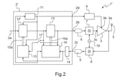
- FIG. 2 it can be seen that there is shown a system for the envelope tracking technique 1 'comprising a baseband linearization system 2' according to a second variant of FIG. invention.
- the system for the envelope tracking technique 1 'according to the second variant is identical to the system for the envelope tracking technique 1 according to the first variant, except that, in the second variant, the pre-module digital distortion device 12 'of the linearization system 2' is configured to perform two-dimensional digital pre-distortion.
- the two-dimensional digital pre-distortion module 12 comprises two inputs respectively connected to the first input 2a of the linearization system 2' and to the output of the amplifier supply voltage selection module 11.
- the digital pre-distortion module 12 is thus configured to perform digital pre-distortion as a function of the amplitude of the I and Q components of the signal to be transmitted and of the supply voltage selected by the voltage selection module. amplifier power supply 11.
- the digital pre-distortion module 12 is configured to perform a one-dimensional digital pre-distortion as a function of the amplitude of the I and Q components of the signal to be transmitted.
- the pre-distortion factor to be applied is only dependent on the modulus of the digital complex baseband signal.
- the one-dimensional digital pre-distortion module 12 comprises two inputs I IN and Q IN , respectively receiving the I and Q components of the signal to be transmitted, and two I OUT and Q OUT outputs.
- the one dimensional digital pre-distortion module 12 comprises a module calculation unit 12a configured to calculate the module 12c of the signal to be transmitted from the data received on the I IN and Q IN inputs.
- the one-dimensional digital pre-distortion module 12 further comprises a one-dimensional (1D) digital predistortion unit 12b configured to digitally pre-distort the data received on the I IN and Q IN inputs based on of the module 12c calculated by the module calculation unit 12a, the linearized I and Q components of the signal to be transmitted being delivered to the I OUT and Q OUT outputs.
- a one-dimensional (1D) digital predistortion unit 12b configured to digitally pre-distort the data received on the I IN and Q IN inputs based on of the module 12c calculated by the module calculation unit 12a, the linearized I and Q components of the signal to be transmitted being delivered to the I OUT and Q OUT outputs.
- the digital pre-distortion module 12 ' is configured to carry out a two-dimensional digital pre-distortion as a function of the amplitude of the I and Q components of the signal to be transmitted and as a function of the supply voltage applied to Class G RF power amplifier 3.
- the two-dimensional digital pre-distortion module 12 comprises two inputs I IN and Q IN , respectively receiving the I and Q components of the signal to be transmitted, an additional input 12d' receiving the supply voltage selection signal delivered by the amplifier supply voltage selection module 11, and two I OUT and Q OUT outputs.
- the two-dimensional digital pre-distortion module 12 ' comprises a module calculation unit 12a' configured to calculate the module 12c 'of the signal to be transmitted from the data received on the I IN and Q IN inputs.
- the two-dimensional digital pre-distortion module 12 'further comprises a two-dimensional (2D) digital pre-distortion unit 12b' configured to digitally pre-distort the data received on the I IN and Q IN inputs. as a function of the module 12c 'calculated by the module calculation unit 12a' and as a function of the supply voltage selection signal received on the additional input 12d ', the linearized I and Q components of the signal to be transmitted being delivered on the I OUT and Q OUT outputs.
- 2D two-dimensional digital pre-distortion unit 12b'
- the pre-distortion coefficients are stored in a memory 18 and indexed according to the signal module to be transmitted calculated by the unit of data.
- module calculation 12a a complex multiplier 19 for applying the selected pre-distortion coefficients to the I and Q components of the signal to be transmitted.
- the digital pre-distortion module 1D 12 could also rely on a baseband digital pre-distortion from nonlinear mathematical functions, for example of the polynomial type with memory or Volterra series, without departing from the scope of the present invention.
- FIG. 6 it can be seen that there is shown the 2D digital pre-distortion module 12 'of the linearization system 2' according to the second variant of the invention.
- the pre-distortion coefficients are stored in several memories 18', each memory 18 'corresponding to a power supply voltage.
- G class 3 power amplifier In the case of an embodiment of the 2D digital pre-distortion module 12 'by correspondence tables, the pre-distortion coefficients are stored in several memories 18', each memory 18 'corresponding to a power supply voltage. G class 3 power amplifier.
- the pre-distortion coefficients are indexed according to the signal module to be transmitted calculated by the module calculation unit 12a', a complex multiplier 19 'making it possible to apply the selected pre-distortion coefficients to the I and Q components of the signal to be transmitted.
- the 2D digital pre-distortion module 12 also rely on a baseband digital pre-distortion from non-linear mathematical functions, for example of the memory polynomial type or the Volterra series, without departing from the of the present invention.
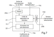
- the pre-distortion coefficient extraction module 15 comprises an output 15a delivering the pre-distortion coefficients to the digital pre-distortion module 12, a first input 15b receiving one of the output of the digital pre-distortion module 12 and the output of the digital filter 13 as a function of the position of the switch 17, a second input 15C receiving the output of the alignment module 14 (corresponding to the output 3a of the power amplifier 3), and a third input 15d receiving the output of the amplifier supply voltage selection module 11.
- the pre-distortion coefficient extraction module 15 comprises first and second time delay units 20a, 20b, a data separation unit 21 and a pre-distortion coefficient extraction unit 22.
- the first time delay unit 20a is configured to compensate for the delay and processing of the signal from one of the complex coefficient digital filter 13 and the digital pre-distortion module 12.
- the second time delay unit 20b is configured to compensate for the delay and processing of the signal from the output of the amplifier supply voltage selection module 11.
- the data separation unit 21 is configured to separate and store in a memory the data relating to the baseband digital signal from the output of the alignment module 14 (corresponding to the output 3a of the power amplifier 3 ) and the delayed signal from one of the complex coefficient digital filter 13 and the digital pre-distortion module 12 as a function of the delayed supply voltage selection signal output from the supply voltage selection module.
- amplifier 11 In the case of class G amplification, the number of possible supply voltages being very low, this task is without complexity and requires few digital resources.
- the pre-distortion coefficient extraction unit 22 is configured to extract, for each possible supply voltage of the power amplifier 3, the associated pre-distortion coefficients from the data stored in memory by the data separation unit 21.
- the extracted pre-distortion coefficients, for each discrete power supply voltage, are then loaded differently into the digital pre-distortion module 12, 12 'depending on whether it is a pre-distortion -distorsion numerical one or two dimensions.
- the pre-distortion coefficients are stored in a single memory zone 18 if the digital pre-distortion module 12 is to one dimension or in as many memory areas 18 'as supply voltages used if the digital pre-distortion module 12' is two-dimensional.
- the process of extracting the pre-distortion coefficients is carried out at predetermined time intervals in order to refine over time the pre-distortion coefficients and thus to obtain increased performances in linearity of the power amplifier of the pre-distortion coefficients.
- Class G 3 The process of continuous extraction of the pre-distortion coefficients also makes it possible to take into account variations in the operating conditions of the power amplifier 3 such as antenna mismatch or temperature variations.
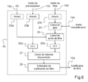
- the filter coefficient extraction module 16 comprises an output 16a delivering the filter coefficients to the complex coefficient digital filter 13, a first input 16b receiving the I and Q components of the input signal to be transmitted, a second input 16c receiving the output of the pre-distortion module 12, a third input 16d receiving the output of the complex coefficient digital filter 13 and a fourth input 16e receiving the output of the alignment module 14 (corresponding to the output 3a of the power amplifier 3).
- the filter coefficient extraction module 16 comprises three time delay units 23a, 23b, 23c, a gain calculation unit 24, an expected filter output signal calculation unit 25, two fast Fourier transform units. (FFT) 26a, 26b, a filter frequency response calculation unit 27 and a filter coefficient extraction unit 28.
- FFT fast Fourier transform
- the three time delay units 23a, 23b, 23c are respectively configured to compensate for the propagation and processing delays of the I and Q components of the signal to be transmitted, the output of the digital pre-distortion module 12 and the output of the filter. Numerical with complex coefficients 13.
- the gain calculating unit 24 is configured to calculate the complex gain of the power amplifier 3 from the delayed output of the complex coefficient digital filter 13 and the baseband digital signal from the output of the d module. 14 alignment (corresponding to the output 3a of the power amplifier 3).
- the expected filter output signal calculation unit 25 is configured to calculate the signal to be generated by the digital filter 13 from the complex gain calculated by the gain calculation unit 24 and the delayed I and Q components of the signal to emit.
- the two FFT units 26a, 26b are respectively configured to calculate the fast Fourier transforms of the delayed output of the digital pre-distortion module 12 and the signal to be generated by the digital filter 13 calculated by the expected signal calculation unit of FIG. filter outlet 25.
- the filter frequency response calculation unit 27 is configured to calculate the frequency response of the digital filter 13 to be generated from the two fast Fourier transforms calculated by the two FFT units 26a, 26b.
- the filter coefficient extraction unit 28 is configured to extract the complex coefficients of the digital filter 13 to be synthesized according to the frequency response calculated by the filter frequency response calculation unit 27.
- digital pre-distortion module 12 must have been previously applied before proceeding to the extraction of the coefficients of the complex digital filter 13.
- the gain calculation unit 24 makes it possible to calculate the complex gain of the power amplifier 3 at each sampling instant according to the equation:
- Amplifier OUT is the output signal of the power amplifier 3 and FLT OUT is the output signal of the complex coefficient digital filter 13.
- the new linearization signal to be generated is calculated for each sampling instant in order to cancel the residual spectral distortions according to the equation:
- Original Waveform is the original signal to be sent and New FLT OUT is the new output of the complex coefficient digital filter 13 to be generated.
- the Fourier transforms of the new linearization signal to be generated calculated previously and the signal from the digital pre-distortion module 12 are calculated on a number of predefined samples according to the equations:
- TFD denotes the discrete Fourier transform function of a sampled signal, this function being implemented using a Fast Fourier Transform (FFT) algorithm
- FFT Fast Fourier Transform
- f denotes the index of the sample after transform Fourrier
- DPD OUT is the output of the digital pre-distortion module 12
- New FLT OUT spectrum is the Fourier transform of the new filter output 13 to generate
- DPD OUT spectrum is the Fourier transform of the output of the module. digital pre-distortion 12.
- the frequency response H of the digital filter 13 to be generated is then estimated in the filter frequency response calculation unit 27 according to the equation:
- f is the index of the sample after Fourier transform, this index corresponding to a frequency index.
- the filter coefficients extraction unit 28 makes it possible to calculate the complex coefficients of the digital filter 13 to be synthesized.
- the calculation of the filter coefficients is performed iteratively at predetermined time intervals, the filter coefficients being refined over successive iterations.
- the filter coefficient extraction module 16 indeed needs several iterations to extract the coefficients of the filter.
- the coefficients of the digital filter 13 are updated over the iterations until linearity performances are obtained in accordance with the standards of the signals to be transmitted. This method makes it possible to refine over time the coefficients of the complex digital filter 13 and thus to obtain increased performances in linearity of the class G 3 RF power amplifier, but also to take account of variations in the operating conditions. of the power amplifier 3 such as antenna mismatch or temperature variations.
- FIG. 9 it can be seen that there is shown the complex coefficient numerical filter 13 of the linearization system 2 according to a first embodiment of the invention.
- the output y of the complex coefficient digital filter 13 is expressed in the following manner as a function of the input signal x :
- the complex coefficient digital filter 13 comprises two identical first finite impulse response (FIR) filters A 29a, 29b whose coefficients correspond to the real part of the complex coefficients of the complex coefficient digital filter 13, two identical second FIR filters B 30a, 30b whose coefficients correspond to the imaginary part of the complex coefficients of the complex coefficient digital filter 13, a subtractor 31 and an adder 32.
- FIR finite impulse response
- the complex coefficient digital filter 13 comprises two inputs I IN and Q IN , respectively receiving the I and Q components of the signal coming from the output of the digital pre-distortion module 12, and two I OUT and Q OUT outputs, respectively delivering the I and Q components after filtering.
- the first FIR A filter 29a receives as input the component I of the output signal of the digital pre-distortion module 12.
- the second FIR B filter 30a receives as input the Q component of the output signal of the digital pre-distortion module 12.
- the first FIR A filter 29a and the second FIR B filter 30a are connected at the output to the subtractor 31 so as to create the component I of the output signal I OUT of the complex coefficient digital filter 13.
- the first FIR A filter 29b receives as input the Q component of the output signal of the digital pre-distortion module 12.
- the second FIR B filter 30b receives as input the component I of the output signal of the digital pre-distortion module 12.
- the first FIR A filter 29b and the second FIR B filter 30b are outputted to the adder 32 so as to create the Q component of the output signal Q OUT of the complex coefficient digital filter 13.
- the first FIR A filters 29a, 29b receive as coefficients the real part of the coefficients C (k) of the synthesized complex digital filter 13 noted C I (k) and the second FIR filters B receive as coefficients the imaginary part of the coefficients C ( k) synthesized complex digital filter 13 denoted by C Q (k) .
- phase output signal denoted I OUT of the digital filter 13 is expressed in the following manner as a function of the input data in phase I IN and in quadrature Q IN :
- the quadrature output signal denoted Q OUT of the digital filter 13 is expressed in the following manner as a function of the input data in phase I IN and in quadrature Q IN :
- M is the number of coefficients of the digital filter 13
- C I (k) and C Q (k) being the respective coefficients of the first filters FIR A and second filters FIR B.
- FIG. 10 it can be seen that there is shown the complex coefficient digital filter 13 of the linearization system 2 according to a second embodiment of the invention.
- the complex coefficient digital filter 13 comprises a first FIR A filter 33 whose coefficients correspond to the sum of the real and imaginary parts of the coefficients of the complex coefficient digital filter 13, a second FIR B filter 34 of which the coefficients correspond to the imaginary part of the coefficients of the complex coefficient digital filter 13, a third FIR C filter 35 whose coefficients correspond to the difference between the real part and the imaginary part of the coefficients of the complex coefficient digital filter 13, two adders 36, 38 and a subtracter 37.
- the first FIR A filter 33 receives as coefficients, denoted by C Filter-A (k), the sum of the real and imaginary part of the coefficients C (k) of the digital filter 13:
- the second FIR B filter 34 receives as coefficients, denoted by C Filter_B (k), the imaginary part of the coefficients C (k) of the digital filter 13:
- the third filter FIR C 35 receives as coefficients, denoted by C Filter_C (k), the difference between the real and imaginary part of the coefficients C (k) of the digital filter 13:
- the complex coefficient digital filter 13 comprises two inputs I IN and Q IN , respectively receiving the I and Q components of the signal coming from the output of the digital pre-distortion module 12, and two I OUT and Q OUT outputs, respectively delivering the I and Q components after filtering.
- the first FIR A filter 33 receives as input the component I of the output signal of the digital pre-distortion module 12.
- the third FIR C filter 35 receives as input the Q component of the output signal of the digital pre-distortion module 12.
- the second FIR B filter 34 receives as input the sum of the I and Q components of the output signal of the digital pre-distortion module 12 via the adder 36.
- the outputs of the first FIR A filter 33 and the second FIR B filter 34 are connected to the subtracter 37 so as to create the component I of the output signal I OUT of the complex coefficient digital filter 13.
- the outputs of the second filter FIR B 34 and the third filter FIR C 35 are connected to the adder 38 so as to create the Q component of the output signal Q OUT of the complex coefficient digital filter 13.
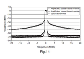
- Figures 11 to 14 show measurement results as an example of an implementation of the linearization system 2 according to the present invention.
- the class G RF power amplifier 3 may have significant variations in the power gain and the phase shift of the amplifier 3 between the different discrete supply voltages provided by the DC-DC converter 4. These variations in gain and phase then lead to significant distortions of the signal to be emitted.
- the response of the Class G 3 RF power amplifier has different gain and phase characteristics between each of the discrete power supply voltages.
- the purpose of the digital pre-distortion module 12 is to correct the gain and the phase specific to each discrete power supply voltage with respect to identical gain and phase target values for all the discrete power supply voltages.
- Figure 11 illustrates, in the case of the one-dimensional digital pre-distortion module 12, the process performed by the pre-distortion coefficient extraction module 15.
- the black-dot cloud represents the input measured data of the data separation unit 21 of the pre-calculation coefficient extraction module.
- distortion 15 and the white dot curve represents the response of the digital pre-distortion module 12 using the pre-distortion coefficients that have been extracted separately for each discrete power supply voltage.
- the response of the class G 3 RF power amplifier coupled to the one-dimensional digital pre-distortion module 12 is then measured in order to extract the coefficients of the complex coefficient digital filter 13 by the extraction module. of filter coefficients 16.
- the modulated signal to be transmitted has, in the case of the example shown in FIGS. 11 to 14, a bandwidth of 1.3 MHz, the generation and acquisition bandwidth extending over a frequency range of 40 MHz. .
- the frequency response of the complex coefficient digital filter 13 to be extracted is then determined by the frequency response calculation unit 27 within the filter coefficient extraction module 16.
- FIGS. 12 and 13 it can be seen that there are illustrated graphs by way of example representing respectively the modulus of the gain (in dB) of the complex coefficient digital filter 13 to be synthesized and the phase (in degree) of the gain of the digital filter with complex coefficients 13 to be synthesized as a function of the frequency (in MHz).
- Figures 12 and 13 illustrate the transfer function in terms of modulus and phase of the complex coefficient filter 13 to be synthesized in order to linearize the class G 3 RF power amplifier.
- the coefficients of the filter 13 are extracted by the filter coefficients extraction unit 28 and implemented in the complex coefficient digital filter 13.
- the curves in solid lines in FIGS. 12 and 13 represent the frequency response of the complex coefficient digital filter 13 synthesized using, in the context of this example, sixty-four complex coefficients.
- the implementation of the linearization method makes it possible to extract the parameters of the digital pre-distortion module 12 and the complex coefficient digital filter 13.
- the baseband linearization system 2 according to the invention for an RF power amplifier 3 operating in class G thus eliminates the distortions induced by this mode of operation of the amplifier 3.
- Fig. 14 it can be seen that there is shown as an exemplary graph showing the output spectra (Power in dBm) of the class G 3 RF power amplifier with and without the linearization system 2 of the present invention, depending on the frequency (in MHz).
- the bold bold line represents the measured spectrum of the signal to be emitted.
- the dotted line curve represents the output spectrum of the class G 3 RF power amplifier alone, that is, without the linearization system 2 of the invention.
- the non-bold solid line curve represents the spectrum at the output of the class G 3 RF power amplifier coupled to the linearization system 2 according to the invention.
- the linearization system 2 of the invention has made it possible to linearize the class G 3 RF power amplifier by eliminating the distortions induced by the class G operating mode of the amplifier 3.
Landscapes
- Engineering & Computer Science (AREA)
- Power Engineering (AREA)
- Physics & Mathematics (AREA)
- Nonlinear Science (AREA)
- Algebra (AREA)
- General Physics & Mathematics (AREA)
- Mathematical Analysis (AREA)
- Mathematical Optimization (AREA)
- Pure & Applied Mathematics (AREA)
- Amplifiers (AREA)
Priority Applications (6)
| Application Number | Priority Date | Filing Date | Title |
|---|---|---|---|
| KR1020207033943A KR20210003223A (ko) | 2018-04-25 | 2019-04-23 | G급 무선주파수 전력 증폭기를 위한 베이스밴드 선형화 시스템 및 방법 |
| US17/050,220 US11356065B2 (en) | 2018-04-25 | 2019-04-23 | System and method of baseband linearization for a class G radiofrequency power amplifier |
| JP2021508340A JP2022502885A (ja) | 2018-04-25 | 2019-04-23 | クラスg高周波パワー・アンプ向けのベースバンド線形化のシステム及び方法 |
| CN201980028178.8A CN112042118A (zh) | 2018-04-25 | 2019-04-23 | 用于g类射频功率放大器的基带线性化的系统和方法 |
| EP19724936.0A EP3785367B1 (de) | 2018-04-25 | 2019-04-23 | System und verfahren zur basisbandlinearisierung für einen hochfrequenzleistungsverstärker der klasse g |
| CH01050/20A CH716092B1 (fr) | 2018-04-26 | 2019-04-24 | Barillet d'horlogerie et procédé de modification de mouvement horloger. |
Applications Claiming Priority (2)
| Application Number | Priority Date | Filing Date | Title |
|---|---|---|---|
| FR1853628A FR3080723B1 (fr) | 2018-04-25 | 2018-04-25 | Systeme et procede de linearisation en bande de base pour un amplificateur de puissance radiofrequence de classe g |
| FR18/53628 | 2018-04-25 |
Publications (1)
| Publication Number | Publication Date |
|---|---|
| WO2019207476A1 true WO2019207476A1 (fr) | 2019-10-31 |
Family
ID=63557557
Family Applications (1)
| Application Number | Title | Priority Date | Filing Date |
|---|---|---|---|
| PCT/IB2019/053335 Ceased WO2019207476A1 (fr) | 2018-04-25 | 2019-04-23 | Systeme et procede de linearisation en bande de base pour un amplificateur de puissance radiofrequence de classe g |
Country Status (7)
| Country | Link |
|---|---|
| US (1) | US11356065B2 (de) |
| EP (1) | EP3785367B1 (de) |
| JP (1) | JP2022502885A (de) |
| KR (1) | KR20210003223A (de) |
| CN (1) | CN112042118A (de) |
| FR (1) | FR3080723B1 (de) |
| WO (1) | WO2019207476A1 (de) |
Families Citing this family (6)
| Publication number | Priority date | Publication date | Assignee | Title |
|---|---|---|---|---|
| US10972139B1 (en) * | 2020-04-15 | 2021-04-06 | Micron Technology, Inc. | Wireless devices and systems including examples of compensating power amplifier noise with neural networks or recurrent neural networks |
| US11496341B2 (en) | 2020-08-13 | 2022-11-08 | Micron Technology, Inc. | Wireless devices and systems including examples of compensating I/Q imbalance with neural networks or recurrent neural networks |
| CN112600571B (zh) * | 2020-12-15 | 2022-04-15 | 维沃移动通信有限公司 | 同步电路、终端及包络跟踪补偿方法 |
| CN113726701B (zh) * | 2021-09-14 | 2023-09-26 | 上海橙科微电子科技有限公司 | 应用于数据传输系统中消除信道反射的系统及方法 |
| CN114217121A (zh) * | 2021-12-08 | 2022-03-22 | 通鼎互联信息股份有限公司 | 一种确定射频额定平均功率的电气实验方法 |
| CN119675659B (zh) * | 2024-11-29 | 2025-11-25 | 成都沃特塞恩电子技术有限公司 | 射频电源及其测试分析方法 |
Citations (4)
| Publication number | Priority date | Publication date | Assignee | Title |
|---|---|---|---|---|
| US20010001546A1 (en) * | 1999-03-09 | 2001-05-24 | Ahuja Bhupendra K. | Power efficient line driver |
| US20100073088A1 (en) * | 2006-03-17 | 2010-03-25 | Nujira Limited | Joint optimisation of supply and bias modulation |
| US20100277236A1 (en) * | 2008-01-15 | 2010-11-04 | Mitsubishi Electric Corporation | Predistorter |
| US20140118065A1 (en) * | 2012-10-30 | 2014-05-01 | Eta Devices, Inc. | Linearization Circuits And Methods For Multilevel Power Amplifier Systems |
Family Cites Families (37)
| Publication number | Priority date | Publication date | Assignee | Title |
|---|---|---|---|---|
| US3772606A (en) | 1972-01-28 | 1973-11-13 | United Aircraft Corp | Multi-level power amplifier |
| JP4597100B2 (ja) * | 1997-09-05 | 2010-12-15 | 富士通株式会社 | 高周波電力増幅器用非線形補償回路 |
| US6236837B1 (en) * | 1998-07-30 | 2001-05-22 | Motorola, Inc. | Polynomial Predistortion linearizing device, method, phone and base station |
| US6298097B1 (en) | 1999-05-11 | 2001-10-02 | Wiseband Communications Inc. | Amplifier with wideband digital predistortion |
| US8811917B2 (en) * | 2002-05-01 | 2014-08-19 | Dali Systems Co. Ltd. | Digital hybrid mode power amplifier system |
| KR100480278B1 (ko) | 2002-12-24 | 2005-04-07 | 삼성전자주식회사 | 광대역 전력 증폭기를 위한 디지털 전치보상기 및 그적응화 방법 |
| US6985706B2 (en) | 2003-01-23 | 2006-01-10 | Powerwave Technologies, Inc. | Feed forward amplifier system employing self-generating alignment lists and adaptive controller |
| US7289773B2 (en) | 2003-01-23 | 2007-10-30 | Powerwave Technologies, Inc. | Digital transmitter system employing self-generating predistortion parameter lists and adaptive controller |
| US7149257B2 (en) | 2003-07-03 | 2006-12-12 | Powerwave Technologies, Inc. | Digital predistortion system and method for correcting memory effects within an RF power amplifier |
| US7259630B2 (en) * | 2003-07-23 | 2007-08-21 | Andrew Corporation | Elimination of peak clipping and improved efficiency for RF power amplifiers with a predistorter |
| US7366252B2 (en) | 2004-01-21 | 2008-04-29 | Powerwave Technologies, Inc. | Wideband enhanced digital injection predistortion system and method |
| US7336725B2 (en) | 2004-03-03 | 2008-02-26 | Powerwave Technologies, Inc. | Digital predistortion system and method for high efficiency transmitters |
| US8068557B2 (en) | 2005-02-24 | 2011-11-29 | Telefonaktiebolaget L M Ericsson (Publ) | IQ-modulator pre-distortion |
| CN100576724C (zh) * | 2005-05-18 | 2009-12-30 | 株式会社Ntt都科摩 | 幂级数型前置补偿器及其控制方法 |
| FI20065783A0 (sv) | 2006-12-08 | 2006-12-08 | Nokia Corp | Signalfördistorsion i radiosändare |
| JP2008177899A (ja) * | 2007-01-19 | 2008-07-31 | Sumitomo Electric Ind Ltd | 増幅回路及び無線通信装置 |
| US8019015B2 (en) | 2007-02-26 | 2011-09-13 | Harris Corporation | Linearization of RF power amplifiers using an adaptive subband predistorter |
| US8005162B2 (en) | 2007-04-20 | 2011-08-23 | Microelectronics Technology, Inc. | Dynamic digital pre-distortion system |
| JP5233651B2 (ja) | 2008-12-18 | 2013-07-10 | 富士通株式会社 | 歪補償装置及び方法 |
| US8159295B2 (en) | 2009-05-21 | 2012-04-17 | The Regents Of The University Of California | Supply-modulated RF power amplifier and RF amplification methods |
| EP2290811A1 (de) | 2009-08-05 | 2011-03-02 | STmicroelectronics SA | Digitaler Vorverzerrer für einen variablen Lieferungsverstärker |
| CN102025327B (zh) * | 2009-09-18 | 2013-01-02 | 富士通株式会社 | 放大器装置和预失真控制方法 |
| EP2502345A1 (de) * | 2009-11-16 | 2012-09-26 | Innovaradio S.A. | Adaptives digitales vorverzerrungsverfahren und vorrichtung zur erhöhung der leistungsversorgung von leistungsverstärkern bei drahtlosen digitalen kommunikationsanwendungen |
| US9041464B2 (en) * | 2011-09-16 | 2015-05-26 | Qualcomm Incorporated | Circuitry for reducing power consumption |
| KR101821294B1 (ko) * | 2011-09-21 | 2018-01-23 | 삼성전자주식회사 | 감소된 대역폭 이티 및 디피디 처리장치 및 그 처리방법 |
| WO2013044238A1 (en) | 2011-09-22 | 2013-03-28 | Dali Systems Co. Ltd. | System and method for increasing bandwidth for digital predistortion in multi-channel wideband communication systems |
| US8798559B2 (en) | 2012-02-28 | 2014-08-05 | Telefonaktiebolaget L M Ericsson (Publ) | FIR/IIR filter predistorter for power amplifiers exhibiting short-term and/or long-term memory effects |
| JP2013239962A (ja) * | 2012-05-16 | 2013-11-28 | Panasonic Corp | 電力増幅装置 |
| US8913689B2 (en) | 2012-09-24 | 2014-12-16 | Dali Systems Co. Ltd. | Wide bandwidth digital predistortion system with reduced sampling rate |
| JP6098336B2 (ja) | 2012-09-25 | 2017-03-22 | 住友電気工業株式会社 | 歪補償装置および無線通信装置 |
| US8824978B2 (en) | 2012-10-30 | 2014-09-02 | Eta Devices, Inc. | RF amplifier architecture and related techniques |
| US8953711B2 (en) | 2013-06-04 | 2015-02-10 | Qualcomm Incorporated | Configurable pre-emphasis component for transmission circuitry |
| US20140362949A1 (en) | 2013-06-11 | 2014-12-11 | Analog Devices Technology | Reduced bandwidth digital predistortion |
| GB2519361B (en) * | 2013-10-21 | 2015-09-16 | Nujira Ltd | Reduced bandwidth of signal in an envelope path for envelope tracking system |
| CN104539246B (zh) | 2015-01-04 | 2017-08-29 | 华为技术有限公司 | 基于包络跟踪的数字预畸变系统、射频系统和方法 |
| US9088472B1 (en) | 2015-01-08 | 2015-07-21 | Freescale Semiconductor, Inc. | System for compensating for I/Q impairments in wireless communication system |
| US10116341B1 (en) * | 2017-06-30 | 2018-10-30 | Intel IP Corporation | Polar transmitter with joined modulator |
-
2018
- 2018-04-25 FR FR1853628A patent/FR3080723B1/fr active Active
-
2019
- 2019-04-23 JP JP2021508340A patent/JP2022502885A/ja active Pending
- 2019-04-23 EP EP19724936.0A patent/EP3785367B1/de active Active
- 2019-04-23 KR KR1020207033943A patent/KR20210003223A/ko not_active Ceased
- 2019-04-23 WO PCT/IB2019/053335 patent/WO2019207476A1/fr not_active Ceased
- 2019-04-23 CN CN201980028178.8A patent/CN112042118A/zh active Pending
- 2019-04-23 US US17/050,220 patent/US11356065B2/en active Active
Patent Citations (4)
| Publication number | Priority date | Publication date | Assignee | Title |
|---|---|---|---|---|
| US20010001546A1 (en) * | 1999-03-09 | 2001-05-24 | Ahuja Bhupendra K. | Power efficient line driver |
| US20100073088A1 (en) * | 2006-03-17 | 2010-03-25 | Nujira Limited | Joint optimisation of supply and bias modulation |
| US20100277236A1 (en) * | 2008-01-15 | 2010-11-04 | Mitsubishi Electric Corporation | Predistorter |
| US20140118065A1 (en) * | 2012-10-30 | 2014-05-01 | Eta Devices, Inc. | Linearization Circuits And Methods For Multilevel Power Amplifier Systems |
Also Published As
| Publication number | Publication date |
|---|---|
| FR3080723B1 (fr) | 2021-08-06 |
| EP3785367A1 (de) | 2021-03-03 |
| US11356065B2 (en) | 2022-06-07 |
| FR3080723A1 (fr) | 2019-11-01 |
| US20210234515A1 (en) | 2021-07-29 |
| JP2022502885A (ja) | 2022-01-11 |
| KR20210003223A (ko) | 2021-01-11 |
| CN112042118A (zh) | 2020-12-04 |
| EP3785367B1 (de) | 2022-02-23 |
Similar Documents
| Publication | Publication Date | Title |
|---|---|---|
| WO2019207476A1 (fr) | Systeme et procede de linearisation en bande de base pour un amplificateur de puissance radiofrequence de classe g | |
| EP0797294B1 (de) | Verfahren zur Korrektur von nichtlinearen Verzerrungen in einem Verstärker und ein solches Verfahren verwendenden Funksenders | |
| EP0803991B1 (de) | Verfahren zur Optimierung von Funkkommunikation zwischen einer Basisstation und einer Mobilstation | |
| EP0929148A1 (de) | Verfahren und Vorrichtung zur numerischen Linearisierung eines Verstärkers | |
| EP1986333B1 (de) | Linearisierung einer Emissionskette | |
| FR2835120A1 (fr) | Procede et dispositif de preparation de signaux destines a etre compares pour etablir une pre-distorsion sur l'entree d'un amplificateur | |
| FR2798244A1 (fr) | Circuit et procede d'amplification de puissance a rendement eleve autorisant une large gamme de reduction de puissance dynamique | |
| EP1269707B1 (de) | Vorrichtung zur erzeugung eines phasen- und amplitudenmodulierten hochfrequenzsignals | |
| FR2755551A1 (fr) | Amplificateur lineaire de puissance et procede de mise en oeuvre | |
| EP2341614B1 (de) | Linearisierungsvorrichtung für Leistungsverstärker | |
| FR2767429A1 (fr) | Dispositif permettant d'apparier des retards dans un amplificateur de puissance | |
| EP3255802B1 (de) | Vorrichtung und verfahren für die verarbeitung eines signals, das von einem durch einen sender gestörten empfänger empfangen wird | |
| FR2721156A1 (fr) | Circuit de linéarisation à prédistorsion. | |
| FR2669165A1 (fr) | Appareil et procede permettant de faire varier un signal dans l'emetteur d'un emetteur-recepteur. | |
| FR2842043A1 (fr) | Pre-egaliseur non lineaire a controle numerique | |
| EP2854354B1 (de) | Verfahren zur Bestimmung von Störstellen eines Sende- und eines Empfangswegs eines Geräts und dazugehörige Vorrichtung | |
| EP3835811B1 (de) | Verfahren zur entkopplung von signalen in sende-/empfangssystemen | |
| EP3371884B1 (de) | Verfahren zur herstellung einer verstärkungsstufe für variables hüllkurvensignal und verstärkungsstufe | |
| EP2975815B1 (de) | Verfahren zur reduzierung des scheitelfaktors eines breitbandsignals | |
| EP0121446A1 (de) | Schaltung zur Linearisierung eines Hochfrequenzverstärkers mit nichtlinearen komplexen Koeffizienten | |
| EP2028810B1 (de) | Korrektur von Verzerrungen in einem Sender | |
| EP2066023B1 (de) | Breitband-HF-Verstärker, der ein Verzerrungsreduzierungssystem umfasst und entspreches Verzerrungsreduzierungsverfahren | |
| FR3091964A1 (fr) | Dispositif de génération d’un signal modulé et chaine d’émission à radiofréquence associée | |
| FR2939995A1 (fr) | Dispositif et procede de traitement d'un signal, systeme d'emission radiofrequence comportant un tel dispositif | |
| EP1190498B1 (de) | Verfahren und vorrichtung zur abgabe eines funksignals in einem kommunikationssystem mit kodemultiplex-vielfachzugriff |
Legal Events
| Date | Code | Title | Description |
|---|---|---|---|
| 121 | Ep: the epo has been informed by wipo that ep was designated in this application |
Ref document number: 19724936 Country of ref document: EP Kind code of ref document: A1 |
|
| ENP | Entry into the national phase |
Ref document number: 2021508340 Country of ref document: JP Kind code of ref document: A |
|
| NENP | Non-entry into the national phase |
Ref country code: DE |
|
| ENP | Entry into the national phase |
Ref document number: 20207033943 Country of ref document: KR Kind code of ref document: A |
|
| ENP | Entry into the national phase |
Ref document number: 2019724936 Country of ref document: EP Effective date: 20201125 |