WO2019225152A1 - 液分含有電解質充填用セラミックパッケージ - Google Patents
液分含有電解質充填用セラミックパッケージ Download PDFInfo
- Publication number
- WO2019225152A1 WO2019225152A1 PCT/JP2019/013674 JP2019013674W WO2019225152A1 WO 2019225152 A1 WO2019225152 A1 WO 2019225152A1 JP 2019013674 W JP2019013674 W JP 2019013674W WO 2019225152 A1 WO2019225152 A1 WO 2019225152A1
- Authority
- WO
- WIPO (PCT)
- Prior art keywords
- cavity
- ceramic
- substrate body
- package
- external connection
- Prior art date
- Legal status (The legal status is an assumption and is not a legal conclusion. Google has not performed a legal analysis and makes no representation as to the accuracy of the status listed.)
- Ceased
Links
Images




Classifications
-
- H—ELECTRICITY
- H01—ELECTRIC ELEMENTS
- H01G—CAPACITORS; CAPACITORS, RECTIFIERS, DETECTORS, SWITCHING DEVICES, LIGHT-SENSITIVE OR TEMPERATURE-SENSITIVE DEVICES OF THE ELECTROLYTIC TYPE
- H01G2/00—Details of capacitors not covered by a single one of groups H01G4/00-H01G11/00
- H01G2/10—Housing; Encapsulation
- H01G2/106—Fixing the capacitor in a housing
-
- H—ELECTRICITY
- H01—ELECTRIC ELEMENTS
- H01G—CAPACITORS; CAPACITORS, RECTIFIERS, DETECTORS, SWITCHING DEVICES, LIGHT-SENSITIVE OR TEMPERATURE-SENSITIVE DEVICES OF THE ELECTROLYTIC TYPE
- H01G2/00—Details of capacitors not covered by a single one of groups H01G4/00-H01G11/00
- H01G2/10—Housing; Encapsulation
-
- H—ELECTRICITY
- H01—ELECTRIC ELEMENTS
- H01G—CAPACITORS; CAPACITORS, RECTIFIERS, DETECTORS, SWITCHING DEVICES, LIGHT-SENSITIVE OR TEMPERATURE-SENSITIVE DEVICES OF THE ELECTROLYTIC TYPE
- H01G11/00—Hybrid capacitors, i.e. capacitors having different positive and negative electrodes; Electric double-layer [EDL] capacitors; Processes for the manufacture thereof or of parts thereof
- H01G11/78—Cases; Housings; Encapsulations; Mountings
-
- H—ELECTRICITY
- H01—ELECTRIC ELEMENTS
- H01G—CAPACITORS; CAPACITORS, RECTIFIERS, DETECTORS, SWITCHING DEVICES, LIGHT-SENSITIVE OR TEMPERATURE-SENSITIVE DEVICES OF THE ELECTROLYTIC TYPE
- H01G11/00—Hybrid capacitors, i.e. capacitors having different positive and negative electrodes; Electric double-layer [EDL] capacitors; Processes for the manufacture thereof or of parts thereof
- H01G11/78—Cases; Housings; Encapsulations; Mountings
- H01G11/80—Gaskets; Sealings
-
- H—ELECTRICITY
- H01—ELECTRIC ELEMENTS
- H01G—CAPACITORS; CAPACITORS, RECTIFIERS, DETECTORS, SWITCHING DEVICES, LIGHT-SENSITIVE OR TEMPERATURE-SENSITIVE DEVICES OF THE ELECTROLYTIC TYPE
- H01G11/00—Hybrid capacitors, i.e. capacitors having different positive and negative electrodes; Electric double-layer [EDL] capacitors; Processes for the manufacture thereof or of parts thereof
- H01G11/78—Cases; Housings; Encapsulations; Mountings
- H01G11/82—Fixing or assembling a capacitive element in a housing, e.g. mounting electrodes, current collectors or terminals in containers or encapsulations
-
- H—ELECTRICITY
- H01—ELECTRIC ELEMENTS
- H01G—CAPACITORS; CAPACITORS, RECTIFIERS, DETECTORS, SWITCHING DEVICES, LIGHT-SENSITIVE OR TEMPERATURE-SENSITIVE DEVICES OF THE ELECTROLYTIC TYPE
- H01G2/00—Details of capacitors not covered by a single one of groups H01G4/00-H01G11/00
- H01G2/02—Mountings
- H01G2/06—Mountings specially adapted for mounting on a printed-circuit support
-
- H—ELECTRICITY
- H01—ELECTRIC ELEMENTS
- H01G—CAPACITORS; CAPACITORS, RECTIFIERS, DETECTORS, SWITCHING DEVICES, LIGHT-SENSITIVE OR TEMPERATURE-SENSITIVE DEVICES OF THE ELECTROLYTIC TYPE
- H01G2/00—Details of capacitors not covered by a single one of groups H01G4/00-H01G11/00
- H01G2/02—Mountings
- H01G2/06—Mountings specially adapted for mounting on a printed-circuit support
- H01G2/065—Mountings specially adapted for mounting on a printed-circuit support for surface mounting, e.g. chip capacitors
-
- H—ELECTRICITY
- H01—ELECTRIC ELEMENTS
- H01G—CAPACITORS; CAPACITORS, RECTIFIERS, DETECTORS, SWITCHING DEVICES, LIGHT-SENSITIVE OR TEMPERATURE-SENSITIVE DEVICES OF THE ELECTROLYTIC TYPE
- H01G2/00—Details of capacitors not covered by a single one of groups H01G4/00-H01G11/00
- H01G2/10—Housing; Encapsulation
- H01G2/103—Sealings, e.g. for lead-in wires; Covers
-
- H—ELECTRICITY
- H01—ELECTRIC ELEMENTS
- H01G—CAPACITORS; CAPACITORS, RECTIFIERS, DETECTORS, SWITCHING DEVICES, LIGHT-SENSITIVE OR TEMPERATURE-SENSITIVE DEVICES OF THE ELECTROLYTIC TYPE
- H01G2/00—Details of capacitors not covered by a single one of groups H01G4/00-H01G11/00
- H01G2/12—Protection against corrosion
-
- H—ELECTRICITY
- H01—ELECTRIC ELEMENTS
- H01G—CAPACITORS; CAPACITORS, RECTIFIERS, DETECTORS, SWITCHING DEVICES, LIGHT-SENSITIVE OR TEMPERATURE-SENSITIVE DEVICES OF THE ELECTROLYTIC TYPE
- H01G9/00—Electrolytic capacitors, rectifiers, detectors, switching devices, light-sensitive or temperature-sensitive devices; Processes of their manufacture
- H01G9/004—Details
- H01G9/08—Housing; Encapsulation
-
- H—ELECTRICITY
- H10—SEMICONDUCTOR DEVICES; ELECTRIC SOLID-STATE DEVICES NOT OTHERWISE PROVIDED FOR
- H10W—GENERIC PACKAGES, INTERCONNECTIONS, CONNECTORS OR OTHER CONSTRUCTIONAL DETAILS OF DEVICES COVERED BY CLASS H10
- H10W20/00—Interconnections in chips, wafers or substrates
- H10W20/20—Interconnections within wafers or substrates, e.g. through-silicon vias [TSV]
-
- H—ELECTRICITY
- H10—SEMICONDUCTOR DEVICES; ELECTRIC SOLID-STATE DEVICES NOT OTHERWISE PROVIDED FOR
- H10W—GENERIC PACKAGES, INTERCONNECTIONS, CONNECTORS OR OTHER CONSTRUCTIONAL DETAILS OF DEVICES COVERED BY CLASS H10
- H10W20/00—Interconnections in chips, wafers or substrates
- H10W20/40—Interconnections external to wafers or substrates, e.g. back-end-of-line [BEOL] metallisations or vias connecting to gate electrodes
- H10W20/41—Interconnections external to wafers or substrates, e.g. back-end-of-line [BEOL] metallisations or vias connecting to gate electrodes characterised by their conductive parts
- H10W20/43—Layouts of interconnections
-
- H—ELECTRICITY
- H10—SEMICONDUCTOR DEVICES; ELECTRIC SOLID-STATE DEVICES NOT OTHERWISE PROVIDED FOR
- H10W—GENERIC PACKAGES, INTERCONNECTIONS, CONNECTORS OR OTHER CONSTRUCTIONAL DETAILS OF DEVICES COVERED BY CLASS H10
- H10W20/00—Interconnections in chips, wafers or substrates
- H10W20/40—Interconnections external to wafers or substrates, e.g. back-end-of-line [BEOL] metallisations or vias connecting to gate electrodes
- H10W20/49—Adaptable interconnections, e.g. fuses or antifuses
-
- H—ELECTRICITY
- H10—SEMICONDUCTOR DEVICES; ELECTRIC SOLID-STATE DEVICES NOT OTHERWISE PROVIDED FOR
- H10W—GENERIC PACKAGES, INTERCONNECTIONS, CONNECTORS OR OTHER CONSTRUCTIONAL DETAILS OF DEVICES COVERED BY CLASS H10
- H10W70/00—Package substrates; Interposers; Redistribution layers [RDL]
- H10W70/60—Insulating or insulated package substrates; Interposers; Redistribution layers
-
- H—ELECTRICITY
- H10—SEMICONDUCTOR DEVICES; ELECTRIC SOLID-STATE DEVICES NOT OTHERWISE PROVIDED FOR
- H10W—GENERIC PACKAGES, INTERCONNECTIONS, CONNECTORS OR OTHER CONSTRUCTIONAL DETAILS OF DEVICES COVERED BY CLASS H10
- H10W70/00—Package substrates; Interposers; Redistribution layers [RDL]
- H10W70/60—Insulating or insulated package substrates; Interposers; Redistribution layers
- H10W70/62—Insulating or insulated package substrates; Interposers; Redistribution layers characterised by their interconnections
- H10W70/63—Vias, e.g. via plugs
- H10W70/635—Through-vias
-
- H—ELECTRICITY
- H10—SEMICONDUCTOR DEVICES; ELECTRIC SOLID-STATE DEVICES NOT OTHERWISE PROVIDED FOR
- H10W—GENERIC PACKAGES, INTERCONNECTIONS, CONNECTORS OR OTHER CONSTRUCTIONAL DETAILS OF DEVICES COVERED BY CLASS H10
- H10W70/00—Package substrates; Interposers; Redistribution layers [RDL]
- H10W70/60—Insulating or insulated package substrates; Interposers; Redistribution layers
- H10W70/67—Insulating or insulated package substrates; Interposers; Redistribution layers characterised by their insulating layers or insulating parts
- H10W70/68—Shapes or dispositions thereof
-
- H—ELECTRICITY
- H10—SEMICONDUCTOR DEVICES; ELECTRIC SOLID-STATE DEVICES NOT OTHERWISE PROVIDED FOR
- H10W—GENERIC PACKAGES, INTERCONNECTIONS, CONNECTORS OR OTHER CONSTRUCTIONAL DETAILS OF DEVICES COVERED BY CLASS H10
- H10W70/00—Package substrates; Interposers; Redistribution layers [RDL]
- H10W70/60—Insulating or insulated package substrates; Interposers; Redistribution layers
- H10W70/67—Insulating or insulated package substrates; Interposers; Redistribution layers characterised by their insulating layers or insulating parts
- H10W70/69—Insulating materials thereof
- H10W70/692—Ceramics or glasses
-
- H—ELECTRICITY
- H10—SEMICONDUCTOR DEVICES; ELECTRIC SOLID-STATE DEVICES NOT OTHERWISE PROVIDED FOR
- H10W—GENERIC PACKAGES, INTERCONNECTIONS, CONNECTORS OR OTHER CONSTRUCTIONAL DETAILS OF DEVICES COVERED BY CLASS H10
- H10W76/00—Containers; Fillings or auxiliary members therefor; Seals
- H10W76/10—Containers or parts thereof
- H10W76/17—Containers or parts thereof characterised by their materials
- H10W76/18—Insulating materials, e.g. resins, glasses or ceramics
-
- H—ELECTRICITY
- H01—ELECTRIC ELEMENTS
- H01G—CAPACITORS; CAPACITORS, RECTIFIERS, DETECTORS, SWITCHING DEVICES, LIGHT-SENSITIVE OR TEMPERATURE-SENSITIVE DEVICES OF THE ELECTROLYTIC TYPE
- H01G11/00—Hybrid capacitors, i.e. capacitors having different positive and negative electrodes; Electric double-layer [EDL] capacitors; Processes for the manufacture thereof or of parts thereof
- H01G11/10—Multiple hybrid or EDL capacitors, e.g. arrays or modules
-
- H—ELECTRICITY
- H01—ELECTRIC ELEMENTS
- H01G—CAPACITORS; CAPACITORS, RECTIFIERS, DETECTORS, SWITCHING DEVICES, LIGHT-SENSITIVE OR TEMPERATURE-SENSITIVE DEVICES OF THE ELECTROLYTIC TYPE
- H01G11/00—Hybrid capacitors, i.e. capacitors having different positive and negative electrodes; Electric double-layer [EDL] capacitors; Processes for the manufacture thereof or of parts thereof
- H01G11/74—Terminals, e.g. extensions of current collectors
-
- H—ELECTRICITY
- H01—ELECTRIC ELEMENTS
- H01G—CAPACITORS; CAPACITORS, RECTIFIERS, DETECTORS, SWITCHING DEVICES, LIGHT-SENSITIVE OR TEMPERATURE-SENSITIVE DEVICES OF THE ELECTROLYTIC TYPE
- H01G9/00—Electrolytic capacitors, rectifiers, detectors, switching devices, light-sensitive or temperature-sensitive devices; Processes of their manufacture
- H01G9/004—Details
- H01G9/008—Terminals
-
- H—ELECTRICITY
- H01—ELECTRIC ELEMENTS
- H01G—CAPACITORS; CAPACITORS, RECTIFIERS, DETECTORS, SWITCHING DEVICES, LIGHT-SENSITIVE OR TEMPERATURE-SENSITIVE DEVICES OF THE ELECTROLYTIC TYPE
- H01G9/00—Electrolytic capacitors, rectifiers, detectors, switching devices, light-sensitive or temperature-sensitive devices; Processes of their manufacture
- H01G9/28—Structural combinations of electrolytic capacitors, rectifiers, detectors, switching devices with other electric components not covered by this subclass
-
- Y—GENERAL TAGGING OF NEW TECHNOLOGICAL DEVELOPMENTS; GENERAL TAGGING OF CROSS-SECTIONAL TECHNOLOGIES SPANNING OVER SEVERAL SECTIONS OF THE IPC; TECHNICAL SUBJECTS COVERED BY FORMER USPC CROSS-REFERENCE ART COLLECTIONS [XRACs] AND DIGESTS
- Y02—TECHNOLOGIES OR APPLICATIONS FOR MITIGATION OR ADAPTATION AGAINST CLIMATE CHANGE
- Y02E—REDUCTION OF GREENHOUSE GAS [GHG] EMISSIONS, RELATED TO ENERGY GENERATION, TRANSMISSION OR DISTRIBUTION
- Y02E60/00—Enabling technologies; Technologies with a potential or indirect contribution to GHG emissions mitigation
- Y02E60/10—Energy storage using batteries
Definitions
- the present invention provides a liquid component for filling a liquid component-containing electrolyte such as a gel in a cavity opened on the surface of a substrate body made of ceramic and surrounding an electronic component to be mounted in the cavity by the electrolyte.
- a liquid component-containing electrolyte such as a gel
- the present invention relates to a ceramic package for filling an electrolyte.
- a ceramic package in which a ceramic frame is stacked on the peripheral side of the upper surface of a flat ceramic base to form a cavity that opens upward, at least one arc corner (within an arc shape in plan view) of the cavity.
- Proposed ceramic package with arc-shaped cutouts formed by cutting out corners in the outer peripheral direction in plan view and castellation conductors extending vertically along the inner wall surface of the cutouts (For example, refer to Patent Document 1).
- the four conductor pads provided for each of the four corners on the bottom surface of the cavity, through the interlayer conductor portion extending between the ceramic base body and the ceramic frame body on the outer peripheral side, The electrical reliability of the path to another castellation conductor formed on the outer surface of the ceramic substrate is increased.
- the ceramic package has an electronic component such as a capacitor mounted on the four conductor pads in the cavity, and is further filled with a liquid or gel electrolyte around the electronic component and in the cavity.
- the opening of the cavity can be hermetically sealed and used as a battery or an electrochemical cell.
- corrosion starts when the electrolyte comes into contact with a metal part such as tungsten forming the conductor pad from a thin part of the nickel layer and the gold layer coated by plating on the surface exposed to the outside of the conductor pad.
- Such corrosion may reach the other castellation conductor formed on the outer surface of the ceramic substrate through the interlayer conductor portion.
- a leak path is generated in an interlayer conductor or the like located between the ceramic layers, and the airtightness between the inside and the outside of the cavity of the ceramic package is impaired.
- JP 2010-287852 A pages 1 to 10, FIGS. 1 to 4.
- the present invention solves the problems described in the background art, and even if a cavity is filled with a liquid-containing electrolyte, the ceramic package for filling a liquid-containing electrolyte in which the corrosion portion due to the electrolyte does not easily propagate to the outside of the cavity. It is an issue to provide.
- the present invention provides an electrical connection between the electrode pad provided on the bottom surface of the cavity opened on the surface of the substrate body made of ceramic and the external connection terminal provided on the back surface of the substrate body. It was conceived that it was carried out only via via conductors that formed one or more ceramic layers forming the bottom surface of the cavity and forming the back surface of the substrate body.
- the ceramic package for filling a liquid-containing electrolyte of the present invention (Claim 1) is formed by laminating a plurality of ceramic layers, and has a front surface and a back surface facing each other, and a side surface located between the front surface and the back surface.
- a substrate main body a cavity having an opening on the surface of the substrate main body and having a bottom surface and an inner surface, an electrode pad formed on the bottom surface of the cavity, and an external connection terminal formed on the back surface of the substrate main body
- a liquid package-containing electrolyte-filled ceramic package comprising: an electronic component that is mounted after the electrode pad; and a liquid-containing electrolyte that is filled in the cavity including the periphery of the electronic component;
- the electrode pad and the external connection terminal are formed of a ceramic layer or layers that form the bottom surface of the cavity and the back surface of the substrate body along the thickness direction.
- the side surface of the substrate main body has a side conductor extending to a back side end portion of the substrate body, and the external connection terminal is connected to the substrate.
- the following effects (1) to (3) can be obtained.
- the electrode pads and the external connection terminals are electrically connected only through the via conductors, and the ceramic layers are arranged on the outer peripheral side of the bottom surface of the cavity and in the same plane as the bottom surface. Directly joined. That is, the side conductor and the electrode pad are not connected on the side surface of the substrate body.
- the side conductor and the electrode pad are not connected on the side surface of the substrate body.
- the ceramic of the ceramic layer is a high-temperature co-fired ceramic such as alumina or a low-temperature co-fired ceramic such as glass ceramic.
- the electrode pad, the external connection terminal, the via conductor, and the inner layer wiring are tungsten (hereinafter simply abbreviated as W) or molybdenum (hereinafter simply abbreviated as Mo) when the ceramic is alumina or the like.
- W tungsten
- Mo molybdenum
- the ceramic is glass-ceramic or the like, it is made of copper (Cu) or silver (Ag).
- the front and back surfaces of the substrate body (package body) have, for example, a rectangular (rectangular or square) shape in plan view, but are not limited to the rectangular shape.
- the electronic component include a capacitor including a capacitor.
- the electrode pad has, for example, a rectangular shape in plan view, but is not limited thereto.
- the electrode pad may be connected in parallel to the plurality of external connection terminals via a plurality of via conductors.
- the cross-section along the radial direction of the via conductor is any one of a circular shape, an oval shape, an elliptical shape, and a rectangular shape.
- the liquid-containing electrolyte contains a gel-like or liquid component and contains, for example, ionized Na, K, Ca, P, Cl and the like.
- a lithium salt such as lithium tetrafluoroborate, or an acid such as hydrochloric acid, sulfuric acid, or nitric acid dissolved in an organic solvent such as dimethoxyethane or propylene carbonate can be used.
- the gel electrolyte is obtained by impregnating a polymer gel with a liquid electrolyte, and the polymer gel includes polyethylene oxide, polymethyl methacrylate, polyvinylidene fluoride, and the like.
- the ceramic package includes a product region in which the plurality of wiring boards are adjacent to each other vertically and horizontally in a plan view, and an ear portion surrounding the product region and laminating the plurality of ceramic layers. It is also possible to adopt a multi-cavity form (large version).
- a part of the electrode pad is provided between a lower ceramic layer forming the bottom surface of the cavity and an upper ceramic layer laminated immediately above the lower ceramic layer.
- the lower ceramic layer and the upper ceramic layer are directly connected at a position on the outer peripheral side excluding the entry portion in a plan view of the substrate body.
- a ceramic package for filling a liquid-containing electrolyte (Claim 2). According to this, even if a part of the electrode pad has an entry portion that enters between the ceramic layers, the ceramic layers are directly bonded to each other on the outer peripheral side of the entry portion.
- the following effect (4) can be obtained.
- the electrode pad has the entry portion at a part thereof, even an electrode pad having a relatively large area in plan view can be easily arranged on the bottom surface of the cavity and the peripheral side thereof. This can contribute to downsizing of the entire package, and also increases the degree of freedom of the setting position of the via conductor that conducts with the external connection terminal provided on the back surface of the substrate body.
- the cavity has a rectangular shape in plan view, and a pair of the electrode pads is formed on one side of the cavity, or a pair is formed on two sides facing the cavity.
- a liquid package-containing electrolyte filling ceramic package (Claim 3) in which the electrode pads are individually formed is also included.
- the following effect (5) can be obtained.
- an electronic component having two electrodes such as a capacitor such as a capacitor can be efficiently mounted on the bottom surface of the cavity having a relatively small area in plan view.
- the said rectangular shape is a rectangle or a square, or the shape which has a round at these four corners is also included.
- a total of four electrode pads including the entry portion may be formed for each of the four corners on the bottom surface of the cavity.
- the substrate body includes an inner layer wiring formed between a lower ceramic layer that forms the bottom surface of the cavity and a lowermost ceramic layer that forms the back surface of the substrate body.
- the via conductor includes a ceramic package for filling a liquid-containing electrolyte (Claim 4) connected to the electrode pad and the external connection terminal via the inner layer wiring.
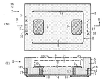
- FIG. 1A is a plan view showing a ceramic package which is an application form of the package of FIG. 1
- FIG. 2B is a vertical sectional view taken along the line BB in FIG.
- FIG. 3A is a plan view showing a ceramic package which is an application form of the package of FIG. 2
- FIG. 3B is a vertical sectional view taken along the line BB in FIG.
- (A), (B) is a top view which shows the wiring board of a different form
- (C) is a partial vertical sectional view which shows the vicinity of the external connection terminal of a different form.
- (A) is a plan view of a multi-purpose wiring board having a plurality of wiring boards of FIG. 1, and (B) is a vertical sectional view taken along the line BB in FIG.
- FIG. 1 (A) is a plan view showing a liquid package-containing electrolyte filling ceramic package 1a according to one embodiment of the present invention
- FIG. 1 (B) is taken along the line BB in FIG. 1 (A). It is a vertical sectional view.
- the liquid package-containing electrolyte filling ceramic package (hereinafter simply referred to as a package) 1a has a rectangular outer shape in plan view and a front surface 3 and a back surface 4 facing each other.
- a substrate body 2 having four side surfaces 5 located between the front surface 3 and the back surface 4, and a bottom surface 7 that opens to the front surface 3 and has a rectangular shape in plan view, and an inner surface that stands up from the four sides.
- a pair (two) of electrode pads 9 formed along the left short side in a plan view of the bottom surface 7 of the cavity 6, and the pair of the back surface 4 of the substrate body 2.
- the substrate body 2 is formed by integrating a flat ceramic layer c1 and a rectangular frame-shaped ceramic layer c2 laminated along the peripheral side of the upper surface of the ceramic layer c1. It is joined.
- the ceramic layers c1 and c2 are mainly composed of alumina, aluminum nitride, mullite, or the like, for example.
- the pair of electrode pads 9 and the pair of external connection terminals 10 can be individually conducted through a pair of via conductors 12 that penetrate the ceramic layer c1 on the lower layer side.
- the pair of via conductors 12 overlap in the front-rear direction of FIG.
- two concave portions 18 each having a rectangular parallelepiped shape extending across the side surface 5 and the back surface 4 are formed on each of the side surfaces 5 on both the left and right sides in a plan view of the substrate body 2.
- the back surface side end portion of the side surface conductor 17 and the side surface of the back surface conductor 11. The side ends are individually connected.
- the electrode pad 9, the external connection terminal 10, the back conductor 11, the via conductor 12, and the side conductor 17 are made of W or Mo.
- a gold layer (not shown) is formed on the surface exposed to the outside via a base nickel layer. It is coated with almost uniform thickness.
- an electronic component 14 such as a capacitor is mounted on the upper side of each electrode pad 9 in the cavity 6, and further includes the periphery of the electronic component 14.
- the cavity 6 is filled with a liquid or gel-like liquid-containing electrolyte (hereinafter simply referred to as an electrolyte) 16.
- the opening of the cavity 6 after being filled with the electrolyte 16 is sealed from the outside, for example, by a cover plate made of ceramic or metal (not shown).
- FIG. 2A is a plan view showing a package 1b having a different form from the package 1a
- FIG. 2B is a vertical sectional view taken along the line BB in FIG. 2A.
- the package 1b includes the same substrate body 2 in which the same ceramic layers c1 and c2 are stacked, and the same cavity 6 as described above.
- a pair of electrode pads 9 are individually formed on a pair of short sides facing each other on the bottom surface 7 of the cavity 6, and a pair on the back surface 4 of the substrate body 2 hits the lower side of each electrode pad 9 in plan view.
- a pair of external connection terminals 10 are formed on the short side.
- a pair of recesses 18 are individually formed across the side surface 5 forming the pair of short sides and the back surface 4 in the substrate body 2 facing in plan view.
- a side conductor 17 is formed for each inner wall on the back side of the recess 18, and the back side end of each side conductor 17 is individually connected to the side end of the pair of external connection terminals 10.
- FIG. 3A is a plan view showing a package 1c which is an application form of the package 1a
- FIG. 3B is a vertical cross-sectional view taken along the line BB in FIG. 3A.
- the package 1c includes a substrate body 2 similar to the package 1a, a cavity 6 similar to the above, and a pair of external connection terminals 10 similar to the above.
- a back conductor 11, a side conductor 17, a via conductor 12, and four recesses 18 are provided.
- the package 1c is different from the package 1a in that the ceramic layer c1 that forms the substrate body 2 on a part of the pair of electrode pads 9 formed along the left short side of the bottom surface 7 of the cavity 6.
- C2 has a structure in which the entry portions 9a are individually included.
- the ceramic layers c1 and c2 are firmly bonded to each other on the outer peripheral side of each of the entry portions 9a.
- FIG. 4A is a plan view showing a package 1d which is an applied form of the package 1b
- FIG. 4B is a vertical sectional view taken along the line BB in FIG. 4A.
- the package 1d includes a substrate body 2 similar to the package 1b, the same cavity 6, and a pair of external connection terminals 10 similar to the above.
- a side conductor 17, a via conductor 12, and a recess 18 are provided.
- the difference between the package 1d and the package 1b is that the substrate body 2 is formed on a part of a pair of electrode pads 9 individually formed on a pair of short sides facing each other on the bottom surface 7 of the cavity 6. This is to have a structure in which the entry portions 9a are individually included between the ceramic layers c1 and c2.
- the ceramic layers c1 and c2 are firmly bonded to each other on the outer peripheral side of each of the entry portions 9a.
- the electrode pad 9 and the external connection terminal 10 are electrically connected only via the via conductor 12, on the outer peripheral side of the bottom surface 7 of the cavity 6 and the bottom surface. In the same plane as 7, the ceramic layers c1 and c2 are directly joined. In addition, the electrode pad 9 and the side conductor 17 are arranged apart from each other and are not directly connected to each other. As a result, it is possible to eliminate or suppress a situation in which a leak path due to corrosion by the electrolyte 16 is formed on the side surface of the substrate body 2.
- the electrolyte 16 that is filled so as to surround the electronic component 14 to be mounted in the cavity 6 from leaking from the outside such as the side surface 5 of the substrate body 2. Further, along with the above, it becomes easy to guarantee the reliability of the electronic component 14 such as a capacitor mounted on the electrode pad 9 provided on the bottom surface 7 of the cavity 6.
- the electrode pad 9 since the electrode pad 9 has the entry portion 9a in a part thereof, the bottom surface 7 of the cavity 6 and the electrode pad 9 having a relatively large area in a plan view can be obtained. Can be easily placed on the peripheral side. As a result, the overall package 1c, 1d can be reduced in size, and the degree of freedom of the position of the via conductor 12 that is electrically connected to the external connection terminal 10 provided on the back surface 4 of the substrate body 2 can be increased. Therefore, according to the ceramics 1c and 1d, in addition to the effects (1) to (3) and (5), the effect (4) can be further obtained.
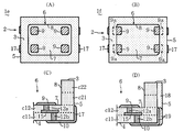
- FIGS. 5A and 5B are plan views schematically showing packages 1e and 1f having different forms from the above-described forms.
- the package 1e includes the same substrate body 2 and the same cavity 6 as those described above.
- Four electrode pads 9 are individually formed on the four corners of the bottom surface 7 of the cavity 6.
- four external connection terminals 10 (Not shown) are individually formed.
- the side surface side end portions for each external connection terminal 10 are individually connected to the back surface side end portions of a total of four side surface conductors 17 formed directly on the pair of left and right side surfaces 5 in FIG. 5A. . Therefore, according to the ceramic 1e, the effects (1) and (2) can be obtained.
- the package 1f includes the same substrate body 2, the same cavity 6, the four electrode pads 9, the four external connection terminals 10 (not shown), and 4 Two side conductors 17 are provided.
- the package 1f is different from the package 1e in that a part of the four electrode pads 9 formed on the four corners of the bottom surface 7 of the cavity 6 are located between the ceramic layers c1 and c2, respectively. It has the structure which has the approach part 9a which approachs separately. Therefore, according to the ceramic 1f, the effects (1) to (4) can be obtained.
- FIGS. 5C and 5D are partial vertical sectional views showing different forms of the substrate body 2.
- the ceramic layer c1 on the lower layer side is further made ceramic layers c11 and c12
- the ceramic layer c2 on the upper layer side is made further ceramic layers c21 and c22, and between the ceramic layers c11 and c12 on the lower layer side.
- an inner layer wiring 15 is formed.
- the electrode pad 9 formed on the inner surface 8 side of the bottom surface 7 of the cavity 6 and the external connection terminal 10 formed on the lower surface 4 on the lower side the upper and lower via conductors 12a and 12b. Can be electrically connected. Accordingly, in plan view, the degree of freedom in design regarding the arrangement of the electrode pads 9 and the external connection terminals 10 can be further increased. In addition to the effects (1) to (3) and (5), Furthermore, the effect (6) can be obtained.
- a recess 18 having a semicircular or semi-oval shape in plan view is formed on the side surface 6 of the substrate body 2 along the entire length in the vertical direction.
- a side conductor 19 having a semicircular arc shape or a semi-long arc shape in plan view connected to the side surface side end portion of the external connection terminal 10 may be formed on the back surface 4 side.
- the electrode pads 9 in FIGS. 5C and 5D may have a configuration in which part of them has the entry portion 9a that enters between the ceramic layers c12 and c21. The effects (1) to (6) can be obtained.
- FIG. 6 (A) is a partial plan view showing a mother package (large plate) 20 for obtaining a large number of packages 1a
- FIG. 6 (B) is an arrow along line BB in FIG. 6 (A). It is a vertical sectional view along the view.
- the mother package 20 is formed by laminating the ceramic layers c1 and c2, and has a front surface 3 and a rear surface 4 that are rectangular in plan view, and a plurality of the packages 1a at the center side in plan view.
- an ear portion 22 having a rectangular frame shape in a plan view surrounding the periphery of the product region 21 is provided.
- the boundary between the product region 21 and the ear portion 22 and the boundary between adjacent packages 1a in the product region 21 are V-shaped in a lattice frame shape in a plan view and a narrow vertical section.
- the dividing grooves 23 having a letter shape are formed in a lattice frame shape in plan view.
- a concave portion 24 having a semicircular shape in plan view is formed on the outer surface of each of the left and right ear portions 22, and a semicircular arc in plan view along the inner wall surface of the concave portion 24.
- a shaped plating electrode 25 is formed.
- the plating electrode 25 is also made of W or Mo.
- the plating electrode 25 is electrically connected to the via conductor 12 or the inner layer wiring 15 through a plating wiring (not shown) formed between the ceramic layers c1 and c2.
- a recess 26 that is open in the back surface 4 and has a rectangular shape in plan view is formed in the vicinity of the back surface 4 of the mother package 20 just below the dividing groove 23.
- the side conductors 17 are individually formed on the left and right inner wall surfaces.
- the side conductor 17 is connected to the external connection terminal 10 or the back conductor 11. That is, when the mother package 20 is divided into pieces along the dividing groove 23, the concave portion 26 is divided into the pair of concave portions 18.
- the multi-package mother package 20 as described above, a plurality of the packages 1a can be efficiently provided (referred to as effect (7)).
- the packages 1b to 1d can also be provided in the form of a mother package having the same form as described above.
- the electrode pad 9 is provided at each of the four corners of the bottom surface 7 of the cavity 6, and the package body as shown in FIG. 5 (D). Even in a form having both the recess 18 and the side conductor 19 on the second side face 5, it can be provided by the mother package having the same form as described above.
- the ceramic layer cx constituting the substrate body 2 may be made of glass-ceramic, for example.
- Cu or Ag is used for conductors such as the electrode pad 9, the external connection terminal 10, the via conductor 12, and the side conductor 17.
- the electrode pads 9 can be formed on the bottom surface 7 of the cavity 6 by an arbitrary total number as long as it is a pair (two or more).
- another side conductor 17 is further formed on the side surface 5 (on the right side in FIGS. 1 and 3) opposite to the side surface 5 on which the side surface conductor 17 is formed in the substrate body 2 of the packages 1a and 1c.
- the external connection terminal 10 having a side surface end connected to the back surface side end of the side conductor 17 may be provided on the right side of the back surface 4.
- the electrode pad 9 corresponding to the right external connection terminal 10 is not necessarily provided above the electrode pad 9.
- one electrode pad 9 is entirely formed on the bottom surface 7, and part of the other electrode pad 9 enters between the ceramic layers c1 and c2. It is good also as a form which has the part 9a.
- a side conductor having a U-shape in plan view may be formed across the three inner wall surfaces of the recesses 18 of the packages 1a to 1d.
- a plurality of cavities 6 are individually opened on the surface 3 of the substrate body 2, and a pair of electrode pads 9 are individually formed on the bottom surface 7 of each cavity 6.
- the external connection terminals 10 and the side conductors 17 connected to the external connection terminals 10 may be formed on the side surfaces 5 adjacent to each other on the back surface 4.
Landscapes
- Engineering & Computer Science (AREA)
- Power Engineering (AREA)
- Microelectronics & Electronic Packaging (AREA)
- Piezo-Electric Or Mechanical Vibrators, Or Delay Or Filter Circuits (AREA)
- Physics & Mathematics (AREA)
- Geometry (AREA)
- Chemical & Material Sciences (AREA)
- Ceramic Engineering (AREA)
Abstract
キャビティ内に電解質を充填しても、該電解質による腐蝕がキャビティの外部へ進展しにくくした液分含有電解質充填用セラミックパッケージを提供する。セラミック製で表・裏面3,4と、これらの間に位置する側面5とを有する基板本体2と、表面3に開口し底面7および内側面8を有するキャビティ6と、底面7に形成した電極パッド9と、裏面4に形成した外部接続端子10と、電極パッド9上に実装される電子部品14と、キャビティ6内に充填される電解質16とを備え、電極パッド9と外部接続端子10とは、キャビティ6の底面7と基板本体2の裏面4とを形成するセラミック層c1を貫通するビア導体12を介して電気的に接続され、基板本体2の側面5には、側面導体17を有し、該側面導体17と外部接続端子10とが接続され、電極パッド9と側面導体17とは、離間して配置されている、液分含有電解質充填用セラミックパッケージ1a。
Description
本発明は、セラミックからなる基板本体の表面に開口するキャビティ内にゲル状などの液分含有電解質を充填して、前記キャビティ内に追って実装される電子部品を前記電解質により包囲するための液分含有電解質充填用セラミックパッケージに関する。
例えば、平板状のセラミック基体の上面の周辺側にセラミック枠体を積層して上方に開口するキャビティを形成したセラミックパッケージにおいて、前記キャビティの少なくとも1つの円弧状角部(平面視が円弧状の内隅部)を平面視で外周側方向に切り欠いて形成した円弧状切り欠き部と、該切り欠き部の内壁面に沿って上下方向に延設するキャスタレーション導体とを設けたセラミックパッケージが提案されている(例えば、特許文献1参照)。
上記セラミックパッケージによれば、上記キャビティの底面における四隅側ごとに設けた4つの導体パッドから、上記セラミック基体と上記セラミック枠体との間を外周側に延出した層間導体部を介して、前記セラミック基体の外側面に形成された別のキャスタレーション導体へ至る経路の電気的信頼性が高められる。
上記セラミックパッケージによれば、上記キャビティの底面における四隅側ごとに設けた4つの導体パッドから、上記セラミック基体と上記セラミック枠体との間を外周側に延出した層間導体部を介して、前記セラミック基体の外側面に形成された別のキャスタレーション導体へ至る経路の電気的信頼性が高められる。
一方、前記セラミックパッケージは、そのキャビティ内における4つの導体パッド上にキャパシタなどの電子部品を実装し、更に該電子部品の周囲で且つ上記キャビティ内に液状やゲル状の電解質を充填した後、当該キャビティの開口部を気密に封止して、電池あるいは電気化学セルとして用いることも可能である。
しかし、前記導体パッドの外部に露出する表面にメッキにより被覆されたニッケル層および金層の薄い部分から上記電解質が該導体パッドを形成するタングステンなどの金属部に接触することにより、腐食が始まると共に、かかる腐食は、前記層間導体部を経て、前記セラミック基体の外側面に形成された前記別のキャスタレーション導体に至る場合がある。その結果、かかる腐蝕が進むと、セラミック層間に位置する層間導体などにリークパスを発生させ、セラミックパッケージのキャビティ内部と外部との気密性が損なわれてしまう、という問題があった。
しかし、前記導体パッドの外部に露出する表面にメッキにより被覆されたニッケル層および金層の薄い部分から上記電解質が該導体パッドを形成するタングステンなどの金属部に接触することにより、腐食が始まると共に、かかる腐食は、前記層間導体部を経て、前記セラミック基体の外側面に形成された前記別のキャスタレーション導体に至る場合がある。その結果、かかる腐蝕が進むと、セラミック層間に位置する層間導体などにリークパスを発生させ、セラミックパッケージのキャビティ内部と外部との気密性が損なわれてしまう、という問題があった。
本発明は、背景技術で説明した問題点を解決し、キャビティ内に液分含有電解質を充填しても、該電解質による腐蝕部分がキャビティの外部へ進展しにくくした液分含有電解質充填用セラミックパッケージを提供する、ことを課題とする。
本発明は、前記課題を解決するため、セラミックからなる基板本体の表面に開口するキャビティの底面に設けた電極パッドと、前記基板本体の裏面に設けた外部接続端子との電気的接続を、上記キャビティの底面を形成し且つ上記基板本体の裏面を形成する単数または複数のセラミック層を貫通するビア導体のみを介して行うようにした、ことに着想して成されたものである。
即ち、本発明の液分含有電解質充填用セラミックパッケージ(請求項1)は、複数のセラミック層を積層してなり、且つ対向する表面および裏面と、該表面と裏面との間に位置する側面とを有する基板本体と、該基板本体の表面に開口し、且つ底面および内側面を有するキャビティと、該キャビティの底面に形成された電極パッドと、上記基板本体の裏面に形成された外部接続端子と、上記電極パッドの上方に追って実装される電子部品と、該電子部品の周囲を含む上記キャビティ内に追って充填される液分含有電解質と、を備える液分含有電解質充填用セラミックパッケージであって、上記電極パッドと上記外部接続端子とは、上記キャビティの底面と上記基板本体の裏面とを形成する単数あるいは複数のセラミック層を厚み方向に沿って貫通するビア導体を介して、電気的に接続されていると共に、上記基板本体の側面には、該側面の裏面側端部まで延在する側面導体を有し、上記外部接続端子は、上記基板本体の裏面の側面側端部まで延在し、且つ上記側面導体の裏面側端部と該外部接続端子の前記側面側端部とが接続されており、上記電極パッドと上記側面導体とは、離間して配置されている、ことを特徴とする。
即ち、本発明の液分含有電解質充填用セラミックパッケージ(請求項1)は、複数のセラミック層を積層してなり、且つ対向する表面および裏面と、該表面と裏面との間に位置する側面とを有する基板本体と、該基板本体の表面に開口し、且つ底面および内側面を有するキャビティと、該キャビティの底面に形成された電極パッドと、上記基板本体の裏面に形成された外部接続端子と、上記電極パッドの上方に追って実装される電子部品と、該電子部品の周囲を含む上記キャビティ内に追って充填される液分含有電解質と、を備える液分含有電解質充填用セラミックパッケージであって、上記電極パッドと上記外部接続端子とは、上記キャビティの底面と上記基板本体の裏面とを形成する単数あるいは複数のセラミック層を厚み方向に沿って貫通するビア導体を介して、電気的に接続されていると共に、上記基板本体の側面には、該側面の裏面側端部まで延在する側面導体を有し、上記外部接続端子は、上記基板本体の裏面の側面側端部まで延在し、且つ上記側面導体の裏面側端部と該外部接続端子の前記側面側端部とが接続されており、上記電極パッドと上記側面導体とは、離間して配置されている、ことを特徴とする。
前記セラミックパッケージによれば、以下の効果(1)~(3)が得られる。
(1)前記電極パッドと前記外部接続端子とは、前記ビア導体のみを介して電気的に接続され、前記キャビティの底面の外周側で且つ該底面と同じ平面では、前記複数のセラミック層同士が直に接合されている。つまり、側面導体と電極パッドとは、基板本体の側面では接続されていない。その結果、前記電解質による腐食に起因するリークパスが基板本体の側面に形成される事態をなくすか、抑制できる。従って、前記キャビティ内に追って実装される電子部品を包囲するように充填される前記液分含有電解質が、前記基板本体の側面などの外部に漏れ出る事態を防止することができる。
(2)上記効果(1)に伴って、前記キャビティの底面に設けた電極パッド上に追って実装されるキャパシタなどの電子部品の信頼性を保証し易くなる。
(3)前記外部接続端子の側面側端部と前記側面導体の裏面側端部とが接続されているので、上記効果(1)と共に、本セラミックパッケージをプリント基板などに搭載する際における接続信頼性を十分に確保することができる。
(1)前記電極パッドと前記外部接続端子とは、前記ビア導体のみを介して電気的に接続され、前記キャビティの底面の外周側で且つ該底面と同じ平面では、前記複数のセラミック層同士が直に接合されている。つまり、側面導体と電極パッドとは、基板本体の側面では接続されていない。その結果、前記電解質による腐食に起因するリークパスが基板本体の側面に形成される事態をなくすか、抑制できる。従って、前記キャビティ内に追って実装される電子部品を包囲するように充填される前記液分含有電解質が、前記基板本体の側面などの外部に漏れ出る事態を防止することができる。
(2)上記効果(1)に伴って、前記キャビティの底面に設けた電極パッド上に追って実装されるキャパシタなどの電子部品の信頼性を保証し易くなる。
(3)前記外部接続端子の側面側端部と前記側面導体の裏面側端部とが接続されているので、上記効果(1)と共に、本セラミックパッケージをプリント基板などに搭載する際における接続信頼性を十分に確保することができる。
尚、前記セラミック層のセラミックは、アルミナなどの高温同時焼成セラミック、あるいはガラスセラミックなどの低温同時焼成セラミックである。
また、前記電極パッド、外部接続端子、ビア導体、および内層配線は、前記セラミックがアルミナなどである場合には、タングステン(以下、単にWと略記する)、あるいはモリブデン(以下、単にMoと略記する)からなり、前記セラミックがガラス-セラミックなどである場合には、銅(Cu)または銀(Ag)からなる。
更に、前記基板本体(パッケージ本体)の表面および裏面は、例えば、平面視で矩形(長方形または正方形)状を呈するが、該矩形状に限定されるものではない。
また、前記電子部品には、例えば、キャパシタを含むコンデンサが例示される。
更に、前記電極パッドは、例えば、平面視が矩形状を呈するが、これに限定されない。
また、前記電極パッドは、複数のビア導体を介して、複数の前記外部接続端子と並列に接続されていても良い。
更に、前記ビア導体の径方向に沿った断面は、円形状、長円形状、楕円形状、矩形状の何れかである。
また、前記電極パッド、外部接続端子、ビア導体、および内層配線は、前記セラミックがアルミナなどである場合には、タングステン(以下、単にWと略記する)、あるいはモリブデン(以下、単にMoと略記する)からなり、前記セラミックがガラス-セラミックなどである場合には、銅(Cu)または銀(Ag)からなる。
更に、前記基板本体(パッケージ本体)の表面および裏面は、例えば、平面視で矩形(長方形または正方形)状を呈するが、該矩形状に限定されるものではない。
また、前記電子部品には、例えば、キャパシタを含むコンデンサが例示される。
更に、前記電極パッドは、例えば、平面視が矩形状を呈するが、これに限定されない。
また、前記電極パッドは、複数のビア導体を介して、複数の前記外部接続端子と並列に接続されていても良い。
更に、前記ビア導体の径方向に沿った断面は、円形状、長円形状、楕円形状、矩形状の何れかである。
また、前記液分含有電解質は、ゲル状あるいは液状の成分を含有し、例えば、イオン化されたNa、K、Ca、P、Clなどを含んでいる。具体的には、四フッ化ホウ酸リチウムなどのリチウム塩、塩酸、硫酸、硝酸などの酸をジメトキシエタンやプロピレンカーボネートなどの有機溶媒に溶解したものが挙げられる。
更に、前記ゲル状の電解質は、液体状の電解質をポリマーゲルに含浸させたもので、該ポリマーゲルには、ポリエチレンオキシド、ポリメタクリル酸メチル、ポリフッ化ビニリデンなどが含まれる。あるいは、ピリジン系、循環式アミン系、脂肪族アミン系、またはイミダゾリウム系のイオン性液体やアミジン系などの常温溶融塩を用いても良い。
加えて、前記セラミックパッケージは、複数の該配線基板を平面視で縦横に隣接して併有する製品領域と、該製品領域の周囲を囲み且つ前記複数のセラミック層を積層した耳部と、から構成された多数個取りの形態(大版)としても良い。
更に、前記ゲル状の電解質は、液体状の電解質をポリマーゲルに含浸させたもので、該ポリマーゲルには、ポリエチレンオキシド、ポリメタクリル酸メチル、ポリフッ化ビニリデンなどが含まれる。あるいは、ピリジン系、循環式アミン系、脂肪族アミン系、またはイミダゾリウム系のイオン性液体やアミジン系などの常温溶融塩を用いても良い。
加えて、前記セラミックパッケージは、複数の該配線基板を平面視で縦横に隣接して併有する製品領域と、該製品領域の周囲を囲み且つ前記複数のセラミック層を積層した耳部と、から構成された多数個取りの形態(大版)としても良い。
また、本発明には、前記キャビティの底面を形成する下層側のセラミック層と、該下層側のセラミック層の真上に積層された上層側のセラミック層との間に、前記電極パッドの一部が進入している進入部を有し、前記基板本体の平面視において該進入部を除いた外周側の位置で前記下層側のセラミック層と前記上層側のセラミック層とが直に接続されている、液分含有電解質充填用セラミックパッケージ(請求項2)も含まれる。
これによれば、前記電極パッドの一部が前記セラミック層同士の間に進入する進入部を有していても、かかる進入部の外周側では、上記セラミック層同士が直に接合されているので、前記効果(1)~(3)を奏することができると共に、更に、以下の効果(4)を得ることも可能となる。
(4)前記電極パッドがその一部に前記進入部を有しているので、平面視が比較的広い面積の電極パッドでも、前記キャビティの底面とその周辺側とに容易に配置できるので、本パッケージ全体の小型化に寄与し得ると共に、基板本体の裏面に設けた前記外部接続端子と導通するビア導体の設定位置の自由度も高められる。
これによれば、前記電極パッドの一部が前記セラミック層同士の間に進入する進入部を有していても、かかる進入部の外周側では、上記セラミック層同士が直に接合されているので、前記効果(1)~(3)を奏することができると共に、更に、以下の効果(4)を得ることも可能となる。
(4)前記電極パッドがその一部に前記進入部を有しているので、平面視が比較的広い面積の電極パッドでも、前記キャビティの底面とその周辺側とに容易に配置できるので、本パッケージ全体の小型化に寄与し得ると共に、基板本体の裏面に設けた前記外部接続端子と導通するビア導体の設定位置の自由度も高められる。
更に、本発明には、前記キャビティは、平面視が矩形状を呈すると共に、該キャビティの一辺側に一対の前記電極パッドが形成されているか、あるいは、前記キャビティで対向する2つの辺側に一対の前記電極パッドが個別に形成されている、液分含有電解質充填用セラミックパッケージ(請求項3)も含まれる。
これによれば、前記各効果に加えて、更に次の効果(5)を得ることができる。
(5)例えば、キャパシタなどのコンデンサのように2つの電極を有する電子部品を、平面視で前記キャビティの比較的狭い面積の底面上に効率良く実装できる。
尚、前記矩形状は、長方形または正方形であるか、あるいは、これらの四隅にアールを有する形状も含んでいる。
また、前記電極パッドは、前記キャビティの底面における四隅側ごとに、前記進入部を含めて合計4個を形成した形態としても良い。
これによれば、前記各効果に加えて、更に次の効果(5)を得ることができる。
(5)例えば、キャパシタなどのコンデンサのように2つの電極を有する電子部品を、平面視で前記キャビティの比較的狭い面積の底面上に効率良く実装できる。
尚、前記矩形状は、長方形または正方形であるか、あるいは、これらの四隅にアールを有する形状も含んでいる。
また、前記電極パッドは、前記キャビティの底面における四隅側ごとに、前記進入部を含めて合計4個を形成した形態としても良い。
加えて、本発明には、前記基板本体は、前記キャビティの底面を形成する下層側のセラミック層と、前記基板本体の裏面を形成す最下層のセラミック層との間に形成された内層配線を有しており、前記ビア導体は、上記内層配線を介して、前記電極パッドおよび前記外部接続端子と接続している、液分含有電解質充填用セラミックパッケージ(請求項4)も含まれる。
これによれば、前記各効果に加えて、更に次の効果(6)を得ることができる。
(6)前記ビア導体が、前記内層配線を介して、前記電極パッドおよび前記外部接続端子と電気的に接続されているので、平面視において、前記電極パッドの配置と、外部接続端子の配置とに関する設計上の自由度が一層高められる。
これによれば、前記各効果に加えて、更に次の効果(6)を得ることができる。
(6)前記ビア導体が、前記内層配線を介して、前記電極パッドおよび前記外部接続端子と電気的に接続されているので、平面視において、前記電極パッドの配置と、外部接続端子の配置とに関する設計上の自由度が一層高められる。
以下において、本発明を実施するための形態について説明する。
図1(A)は、本発明による一形態の液分含有電解質充填用セラミックパッケージ1aを示す平面図、図1(B)は、前記(A)中のB-B線の矢視に沿った垂直断面図である。
上記液分含有電解質充填用セラミックパッケージ(以下、単にパッケージと称する)1aは、図1(A),(B)に示すように、平面視の外形が矩形状で且つ対向する表面3および裏面4と,該表面3と裏面4との間に位置する四辺の側面5とを有する基板本体2と、前記表面3に開口し且つ平面視が矩形状の底面7およびその四辺から立設する内側面8を有するキャビティ6と、該キャビティ6の底面7における平面視で左側の短辺側に沿って形成された一対(2個)の電極パッド9と、上記基板本体2の裏面4における前記一対のパッド9の下方側ごとに個別に形成された一対(2個)の外部接続端子10と、該外部接続端子10とは反対側の前記裏面4に形成された一対の実装用裏面導体(以下、単に裏面導体と称する)11と、を備えている。
図1(A)は、本発明による一形態の液分含有電解質充填用セラミックパッケージ1aを示す平面図、図1(B)は、前記(A)中のB-B線の矢視に沿った垂直断面図である。
上記液分含有電解質充填用セラミックパッケージ(以下、単にパッケージと称する)1aは、図1(A),(B)に示すように、平面視の外形が矩形状で且つ対向する表面3および裏面4と,該表面3と裏面4との間に位置する四辺の側面5とを有する基板本体2と、前記表面3に開口し且つ平面視が矩形状の底面7およびその四辺から立設する内側面8を有するキャビティ6と、該キャビティ6の底面7における平面視で左側の短辺側に沿って形成された一対(2個)の電極パッド9と、上記基板本体2の裏面4における前記一対のパッド9の下方側ごとに個別に形成された一対(2個)の外部接続端子10と、該外部接続端子10とは反対側の前記裏面4に形成された一対の実装用裏面導体(以下、単に裏面導体と称する)11と、を備えている。
前記基板本体2は、図1(B)に示すように、平板形状のセラミック層c1と、該セラミック層c1の上面における周辺側に沿って積層された矩形枠状のセラミック層c2とを一体に接合したものである。該セラミック層c1,c2は、例えば、アルミナ、窒化アルミニウム、またはムライトなどを主成分としている。
また、前記一対の電極パッド9と一対の外部接続端子10とは、下層側の前記セラミック層c1を貫通する一対のビア導体12を介して、個別に導通可能とされている。尚、該一対のビア導体12は、図1(B)の前後方向で重複している。
更に、前記基板本体2における平面視で左右両側の側面5には、該側面5と前記裏面4とに跨がる全体が直方体形状の凹部18が2つずつ形成され、このうち、左側の側面5の凹部18ごとの該側面5と平行な奥側の内壁面には、前記一対の外部接続端子10の側面側端部と裏面側端部が接続される一対の側面導体17が個別に延在している。
加えて、上記基板本体2において、平面視で右側の側面5と裏面4とに跨がって形成された一対の凹部18ごとでは、上記側面導体17の裏面側端部と裏面導体11の側面側端部とが個別に接続されている。
また、前記一対の電極パッド9と一対の外部接続端子10とは、下層側の前記セラミック層c1を貫通する一対のビア導体12を介して、個別に導通可能とされている。尚、該一対のビア導体12は、図1(B)の前後方向で重複している。
更に、前記基板本体2における平面視で左右両側の側面5には、該側面5と前記裏面4とに跨がる全体が直方体形状の凹部18が2つずつ形成され、このうち、左側の側面5の凹部18ごとの該側面5と平行な奥側の内壁面には、前記一対の外部接続端子10の側面側端部と裏面側端部が接続される一対の側面導体17が個別に延在している。
加えて、上記基板本体2において、平面視で右側の側面5と裏面4とに跨がって形成された一対の凹部18ごとでは、上記側面導体17の裏面側端部と裏面導体11の側面側端部とが個別に接続されている。
また、前記電極パッド9、外部接続端子10、裏面導体11、ビア導体12、および側面導体17は、WあるいはMoからなる。これらのうち、上記電極パッド9、外部接続端子10、裏面導体11、側面導体17において、これらの外部に露出する表面には、下地側のニッケル層を介して金層(図示せず)が各々ほぼ均一な厚みで被覆されている。
加えて、図1(B)に示すように、前記キャビティ6内の電極パッド9ごとの上方には、追って、キャパシタのような電子部品14が実装され、更に、該電子部品14の周囲を含む上記キャビティ6内には、液状またはゲル状の液分含有電解質(以下、単に電解質と称する)16が追って充填される。
尚、上記電解質16が充填された後の前記キャビティ6の開口部は、例えば、図示しないセラミック製や金属製などの蓋板によって、外部から密封される。
加えて、図1(B)に示すように、前記キャビティ6内の電極パッド9ごとの上方には、追って、キャパシタのような電子部品14が実装され、更に、該電子部品14の周囲を含む上記キャビティ6内には、液状またはゲル状の液分含有電解質(以下、単に電解質と称する)16が追って充填される。
尚、上記電解質16が充填された後の前記キャビティ6の開口部は、例えば、図示しないセラミック製や金属製などの蓋板によって、外部から密封される。
図2(A)は、前記パッケージ1aと異なる形態のパッケージ1bを示す平面図、図2(B)は前記(A)中のB-B線の矢視に沿った垂直断面図である。
上記パッケージ1bは、図2(A),(B)に示すように、前記同様のセラミック層c1,c2を積層した前記同様の基板本体2と、前記同様のキャビティ6とを備えている。該パッケージ1bでは、キャビティ6の底面7において対向する一対の短辺側に一対の電極パッド9が個別に形成され、平面視で該電極パッド9ごとの下方側に当たる基板本体2の裏面4における一対の短辺側に、一対の外部接続端子10が形成されている。また、平面視で対向する基板本体2における一対の短辺を形成する側面5と前記裏面4とに跨がって、一対の凹部18が個別に形成されている。該凹部18の奥側の内壁面ごとには、側面導体17が形成され、該側面導体17ごとの裏面側端部は、上記一対の外部接続端子10の側面側端部と個別に接続されている。
尚、図2(B)に示すように、前記パッケージ1bでも、そのキャビティ6内に、前記同様の電子部品14が追って実装され、且つその周囲には前記と同様の電解質16が追って充填された後、該キャビティ6の開口部は、適宜封止される。
上記パッケージ1bは、図2(A),(B)に示すように、前記同様のセラミック層c1,c2を積層した前記同様の基板本体2と、前記同様のキャビティ6とを備えている。該パッケージ1bでは、キャビティ6の底面7において対向する一対の短辺側に一対の電極パッド9が個別に形成され、平面視で該電極パッド9ごとの下方側に当たる基板本体2の裏面4における一対の短辺側に、一対の外部接続端子10が形成されている。また、平面視で対向する基板本体2における一対の短辺を形成する側面5と前記裏面4とに跨がって、一対の凹部18が個別に形成されている。該凹部18の奥側の内壁面ごとには、側面導体17が形成され、該側面導体17ごとの裏面側端部は、上記一対の外部接続端子10の側面側端部と個別に接続されている。
尚、図2(B)に示すように、前記パッケージ1bでも、そのキャビティ6内に、前記同様の電子部品14が追って実装され、且つその周囲には前記と同様の電解質16が追って充填された後、該キャビティ6の開口部は、適宜封止される。
図3(A)は、前記パッケージ1aの応用形態であるパッケージ1cを示す平面図、図3(B)は、前記(A)中のB-B線の矢視に沿った垂直断面図である。
上記パッケージ1cは、図3(A),(B)に示すように、前記パッケージ1aと同様の基板本体2と、前記同様のキャビティ6と、前記と同様である一対ずつの外部接続端子10、裏面導体11、側面導体17、ビア導体12、および、4つの凹部18とを備えている。
該パッケージ1cが前記パッケージ1aと相違している点は、キャビティ6の底面7における左側の短辺に沿って形成された一対の電極バッド9の一部に、基板本体2を形成するセラミック層c1,c2間に進入部9aが個別に含まれている構造を有することである。尚、該進入部9aごとの外周側では、前記セラミック層c1,c2が互いに強固に接合されている。
上記パッケージ1cは、図3(A),(B)に示すように、前記パッケージ1aと同様の基板本体2と、前記同様のキャビティ6と、前記と同様である一対ずつの外部接続端子10、裏面導体11、側面導体17、ビア導体12、および、4つの凹部18とを備えている。
該パッケージ1cが前記パッケージ1aと相違している点は、キャビティ6の底面7における左側の短辺に沿って形成された一対の電極バッド9の一部に、基板本体2を形成するセラミック層c1,c2間に進入部9aが個別に含まれている構造を有することである。尚、該進入部9aごとの外周側では、前記セラミック層c1,c2が互いに強固に接合されている。
図4(A)は、前記パッケージ1bの応用形態であるパッケージ1dを示す平面図、図4(B)は、前記(A)中のB-B線の矢視に沿った垂直断面図である。
上記パッケージ1dは、図4(A),(B)に示すように、前記パッケージ1bと同様の基板本体2と、前記同様のキャビティ6と、前記と同様である一対ずつの外部接続端子10、側面導体17、ビア導体12、および、凹部18とを備えている。
該パッケージ1dが前記パッケージ1bと相違している点は、キャビティ6の底面7において対向する一対の短辺に個別に形成された一対の電極バッド9の一部に、前記基板本体2を形成するセラミック層c1,c2間に進入部9aが個別に含まれている構造を有することである。尚、該進入部9aごとの外周側でも、前記セラミック層c1,c2が互いに強固に接合されている。
上記パッケージ1dは、図4(A),(B)に示すように、前記パッケージ1bと同様の基板本体2と、前記同様のキャビティ6と、前記と同様である一対ずつの外部接続端子10、側面導体17、ビア導体12、および、凹部18とを備えている。
該パッケージ1dが前記パッケージ1bと相違している点は、キャビティ6の底面7において対向する一対の短辺に個別に形成された一対の電極バッド9の一部に、前記基板本体2を形成するセラミック層c1,c2間に進入部9aが個別に含まれている構造を有することである。尚、該進入部9aごとの外周側でも、前記セラミック層c1,c2が互いに強固に接合されている。
前記のようなセラミック1a,1bでは、前記電極パッド9と前記外部接続端子10とは、前記ビア導体12のみを介して電気的に接続され、前記キャビティ6の底面7の外周側で且つ該底面7と同じ平面では、前記セラミック層c1,c2同士が直に接合されている。しかも、前記電極パッド9と側面導体17とは、互いに離間して配置されており、両者間は直接接続されていない。その結果、前記電解質16による腐食に起因するリークパスが基板本体2の側面に形成される事態をなくすか、抑制できる。従って、前記キャビティ6内に追って実装される電子部品14を包囲するように追って充填される前記電解質16が、前記基板本体2の側面5などの外部ら漏れ出る事態を防止することができる。
更に、上記に伴って、前記キャビティ6の底面7に設けた電極パッド9上に追って実装されるキャパシタなどの電子部品14の信頼性を保証し易くなる。
加えて、前記外部接続端子10の側面側の端部と前記側面導体17の裏面側の端部とが接続されているので、本セラミックパッケージ1a,1bをプリント基板などに搭載する際における接続信頼性を十分に確保することができる。
従って、前記セラミック1a,1bによれば、前記効果(1)~(3)、(5)を得ることができる。
更に、上記に伴って、前記キャビティ6の底面7に設けた電極パッド9上に追って実装されるキャパシタなどの電子部品14の信頼性を保証し易くなる。
加えて、前記外部接続端子10の側面側の端部と前記側面導体17の裏面側の端部とが接続されているので、本セラミックパッケージ1a,1bをプリント基板などに搭載する際における接続信頼性を十分に確保することができる。
従って、前記セラミック1a,1bによれば、前記効果(1)~(3)、(5)を得ることができる。
また、前記パッケージ1c,1dでは、前記電極パッド9がその一部に前記進入部9aを有しているので、平面視が比較的広い面積の電極パッド9でも、前記キャビティ6の底面7とその周辺側とに容易に配置できる。その結果、上記パッケージ1c,1d全体の小型化に寄与し得ると共に、基板本体2の裏面4に設けた前記外部接続端子10と導通するビア導体12の位置の自由度も高められる。
従って、前記セラミック1c,1dによれば、前記効果(1)~(3)、(5)に加えて、更に前記効果(4)を得ることができる。
従って、前記セラミック1c,1dによれば、前記効果(1)~(3)、(5)に加えて、更に前記効果(4)を得ることができる。
図5(A)、(B)は、前記各形態とは異なる形態のパッケージ1e,1fの概略を示す平面図である。
上記パッケージ1eは、図5(A)に示すように、前記同様の基板本体2と、前記同様のキャビティ6とを備えている。該キャビティ6の底面7における四隅側には、4つの電極パッド9が個別に形成され、これらの下方側である基板本体2の裏面4ごとには、前記同様である4つの外部接続端子10(図示せず)が個別に形成されている。該外部接続端子10ごとの側面側端部は、図5(A)で左右一対の側面5に直に一対ずつ形成された合計4つの側面導体17の裏面側端部と個別に接続されている。
従って、上記セラミック1eによれば、前記効果(1)、(2)を得ることができる。
上記パッケージ1eは、図5(A)に示すように、前記同様の基板本体2と、前記同様のキャビティ6とを備えている。該キャビティ6の底面7における四隅側には、4つの電極パッド9が個別に形成され、これらの下方側である基板本体2の裏面4ごとには、前記同様である4つの外部接続端子10(図示せず)が個別に形成されている。該外部接続端子10ごとの側面側端部は、図5(A)で左右一対の側面5に直に一対ずつ形成された合計4つの側面導体17の裏面側端部と個別に接続されている。
従って、上記セラミック1eによれば、前記効果(1)、(2)を得ることができる。
一方、前記パッケージ1fは、図5(B)に示すように、前記同様の基板本体2、前記同様のキャビティ6、4つの電極パッド9、4つの外部接続端子10(図示せず)、および4つの側面導体17を有している。該パッケージ1fが前記パッケージ1eと相違する点は、図示のように、上記キャビティ6の底面7における四隅側に形成された4つの電極パッド9の一部が、それぞれ前記セラミック層c1,c2間に個別に進入する進入部9aを有している構造にある。
従って、上記セラミック1fによれば、前記効果(1)~(4)を得ることができる。
従って、上記セラミック1fによれば、前記効果(1)~(4)を得ることができる。
図5(C)、(D)は、前記基板本体2の異なる形態を示す部分垂直断面図である。図示すように、下層側の前記セラミック層c1を更にセラミック層c11,c12とし、且つ上層側の前記セラミック層c2を更にセラミック層c21,c22とすると共に、下層側のセラミック層c11,c12の間に内層配線15を更に形成している。その結果、キャビティ6の底面7における内側面8側に形成された電極パッド9と、その下方側の裏面4に形成された外部接続端子10との間を、上下2つのビア導体12a,12bにより電気的に接続することができる。
従って、平面視において、前記電極パッド9の配置と、外部接続端子10との配置に関する設計上の自由度が一層高められるので、前記効果(1)~(3)、(5)に加えて、更に、前記効果(6)を得ることができる。
従って、平面視において、前記電極パッド9の配置と、外部接続端子10との配置に関する設計上の自由度が一層高められるので、前記効果(1)~(3)、(5)に加えて、更に、前記効果(6)を得ることができる。
尚、図5(D)に示すように、基板本体2の側面6に平面視が半円形状あるいは半長円形状の凹部18を垂直方向の全長に沿って形成し、該凹部18の内壁面における裏面4側に、前記外部接続端子10の側面側端部と接続する平面視が半円弧形状あるいは半長円弧形状の側面導体19を形成しても良い。
また、図5(C)、(D)中の電極パッド9は、それらの一部が前記セラミック層c12,c21間に進入する前記進入部9aを有する形態としても良く、かかる形態の場合には、前記効果(1)~(6)を得ることができる。
また、図5(C)、(D)中の電極パッド9は、それらの一部が前記セラミック層c12,c21間に進入する前記進入部9aを有する形態としても良く、かかる形態の場合には、前記効果(1)~(6)を得ることができる。
図6(A)は、前記パッケージ1aを多数個取りにより得るための母パッケージ(大版)20を示す部分平面図、図6(B)は、前記(A)中のB-B線の矢視に沿った垂直断面図である。
上記母パッケージ20は、図示のように、前記セラミック層c1,c2を積層してなり、平面視が矩形状の表面3および裏面4を有すると共に、平面視の中央側には複数の前記パッケージ1aを縦横に隣接して併有する製品領域21と、該製品領域21の周囲を囲む平面視が矩形枠状の耳部22とを備えている。
上記表面3側において、上記製品領域21と耳部22との境界、および製品領域21内で隣接するパッケージ1a同士間の境界には、平面視が格子枠形状で且つ垂直断面が幅の狭いV字形状を呈する分割溝23が平面視で格子枠形状にして形成されている。
上記母パッケージ20は、図示のように、前記セラミック層c1,c2を積層してなり、平面視が矩形状の表面3および裏面4を有すると共に、平面視の中央側には複数の前記パッケージ1aを縦横に隣接して併有する製品領域21と、該製品領域21の周囲を囲む平面視が矩形枠状の耳部22とを備えている。
上記表面3側において、上記製品領域21と耳部22との境界、および製品領域21内で隣接するパッケージ1a同士間の境界には、平面視が格子枠形状で且つ垂直断面が幅の狭いV字形状を呈する分割溝23が平面視で格子枠形状にして形成されている。
また、図6(A)に示すように、左右の耳部22ごとの外側面には、平面視が半円形の凹部24が形成され、該凹部24の内壁面に沿って平面視が半円弧形状のメッキ用電極25が形成されている。該メッキ用電極25もWやMoからなる。
尚、上記メッキ用電極25は、前記セラミック層c1,c2間に形成された図示しないメッキ用配線を介して、前記ビア導体12あるいは前記内層配線15と電気的に接続されている。
更に、図6(B)に示すように、前記母パッケージ20の裏面4における前記分割溝23の真下付近ごとには、該裏面4に開口し且つ平面視が長方形状の凹部26が形成され、それらにおける図示で左右の内壁面ごとには、前記側面導体17が個別に形成されている。該側面導体17は、外部接続端子10または裏面導体11と接続されている。即ち、上記分割溝23に沿って母パッケージ20を個片化した場合、上記凹部26は、一対の前記凹部18に分割されるものである。
尚、上記メッキ用電極25は、前記セラミック層c1,c2間に形成された図示しないメッキ用配線を介して、前記ビア導体12あるいは前記内層配線15と電気的に接続されている。
更に、図6(B)に示すように、前記母パッケージ20の裏面4における前記分割溝23の真下付近ごとには、該裏面4に開口し且つ平面視が長方形状の凹部26が形成され、それらにおける図示で左右の内壁面ごとには、前記側面導体17が個別に形成されている。該側面導体17は、外部接続端子10または裏面導体11と接続されている。即ち、上記分割溝23に沿って母パッケージ20を個片化した場合、上記凹部26は、一対の前記凹部18に分割されるものである。
以上のような多数個取り用の母パッケージ20によれば、複数の前記パッケージ1aを効率良く提供することができる(効果(7)と称する)。
尚、前記パッケージ1b~1dも、前記同様の形態を有する母パッケージの形態によって提供することが可能である。
また、前記図5(A),(B)で示したように、キャビティ6の底面7の四隅側ごとに電極パッド9を有し、且つ前記図5(D)で示したように、パッケージ本体2の側面5に凹部18と側面導体19とを併有する形態であっても、前記同様の形態を有する母パッケージによって提供することが可能である。
尚、前記パッケージ1b~1dも、前記同様の形態を有する母パッケージの形態によって提供することが可能である。
また、前記図5(A),(B)で示したように、キャビティ6の底面7の四隅側ごとに電極パッド9を有し、且つ前記図5(D)で示したように、パッケージ本体2の側面5に凹部18と側面導体19とを併有する形態であっても、前記同様の形態を有する母パッケージによって提供することが可能である。
本発明は、以上において説明した各形態に限定されるものではない。
例えば、前記基板本体2を構成するセラミック層cxは、例えば、ガラス-セラミックからなるものとしても良い。かかる場合、前記電極パッド9、外部接続端子10、ビア導体12、および側面導体17などの導体には、CuまたはAgが用いられる。
また、前記電極パッド9は、一対(2個)以上であれば、任意の総数によって前記キャビティ6の底面7に形成することができる。
更に、前記パッケージ1a,1cの基板本体2において、前記側面導体17が形成された側面5と対向する(図1,図3で右側の)側面5にも、別の側面導体17を更に形成し、該側面導体17の裏面側端部と接続する側面側端部を有する外部接続端子10を前記裏面4の右側に設けても良い。この場合、該右側の外部接続端子10に対応する電極パッド9を必ずしもその上方に設ける必要はない。
例えば、前記基板本体2を構成するセラミック層cxは、例えば、ガラス-セラミックからなるものとしても良い。かかる場合、前記電極パッド9、外部接続端子10、ビア導体12、および側面導体17などの導体には、CuまたはAgが用いられる。
また、前記電極パッド9は、一対(2個)以上であれば、任意の総数によって前記キャビティ6の底面7に形成することができる。
更に、前記パッケージ1a,1cの基板本体2において、前記側面導体17が形成された側面5と対向する(図1,図3で右側の)側面5にも、別の側面導体17を更に形成し、該側面導体17の裏面側端部と接続する側面側端部を有する外部接続端子10を前記裏面4の右側に設けても良い。この場合、該右側の外部接続端子10に対応する電極パッド9を必ずしもその上方に設ける必要はない。
更に、単一の前記キャビティ6の底面7において、一方の電極パッド9全体が該底面7上に形成され、且つ他方の電極パッド9の一部が前記セラミック層c1,c2間などに進入する進入部9aを有している形態としても良い。
また、前記パッケージ1a~1dの凹部18における3つの内壁面に亘って平面視がコ字形状を呈する側面導体を形成しても良い。
加えて、前記基板本体2の表面3に複数のキャビティ6が個別に開口し、且つ該キャビティ6ごとの底面7に一対以上の電極パッド9が個別に形成されていると共に、これらの下方側の裏面4ごとにおいて隣接する側面5に、前記外部接続端子10とこれに接続する側面導体17などとを形成した形態としても良い。
また、前記パッケージ1a~1dの凹部18における3つの内壁面に亘って平面視がコ字形状を呈する側面導体を形成しても良い。
加えて、前記基板本体2の表面3に複数のキャビティ6が個別に開口し、且つ該キャビティ6ごとの底面7に一対以上の電極パッド9が個別に形成されていると共に、これらの下方側の裏面4ごとにおいて隣接する側面5に、前記外部接続端子10とこれに接続する側面導体17などとを形成した形態としても良い。
本発明によれば、キャビティ内に液分含有電解質を充填しても、該電解質による腐蝕部分が外部に進展しにくくした液分含有電解質充填用セラミックパッケージを確実に提供できる。
1a~1f………………パッケージ
2…………………………基板本体
3…………………………表面
4…………………………裏面
5…………………………側面
6…………………………キャビティ
7…………………………底面
8…………………………内側面
9…………………………電極パッド
9a………………………進入部
10………………………外部接続端子
12,12a,12b…ビア導体
14………………………電子部品
15………………………内層配線
16………………………電解質
17,19………………側面導体
c1,c2………………セラミック層
2…………………………基板本体
3…………………………表面
4…………………………裏面
5…………………………側面
6…………………………キャビティ
7…………………………底面
8…………………………内側面
9…………………………電極パッド
9a………………………進入部
10………………………外部接続端子
12,12a,12b…ビア導体
14………………………電子部品
15………………………内層配線
16………………………電解質
17,19………………側面導体
c1,c2………………セラミック層
Claims (4)
- 複数のセラミック層を積層してなり、且つ対向する表面および裏面と、該表面と裏面との間に位置する側面とを有する基板本体と、
上記基板本体の表面に開口し、且つ底面および内側面を有するキャビティと、
上記キャビティの底面に形成された電極パッドと、
上記基板本体の裏面に形成された外部接続端子と、
上記電極パッドの上方に追って実装される電子部品と、該電子部品の周囲を含む上記キャビティ内に追って充填される液分含有電解質と、を備える液分含有電解質充填用セラミックパッケージであって、
上記電極パッドと上記外部接続端子とは、上記キャビティの底面と上記基板本体の裏面とを形成する単数あるいは複数のセラミック層を厚み方向に沿って貫通するビア導体を介して、電気的に接続されていると共に、
上記基板本体の側面には、該側面の裏面側端部まで延在する側面導体を有し、
上記外部接続端子は、上記基板本体の裏面の側面側端部まで延在し、且つ上記側面導体の裏面側端部と該外部接続端子の前記側面側端部とが接続されており、
上記電極パッドと上記側面導体とは、離間して配置されている、
ことを特徴とする液分含有電解質充填用セラミックパッケージ。 - 前記キャビティの底面を形成する下層側のセラミック層と、該下層側のセラミック層の真上に積層された上層側のセラミック層との間に、前記電極パッドの一部が進入している進入部を有し、前記基板本体の平面視において該進入部を除いた外周側の位置で前記下層側のセラミック層と前記上層側のセラミック層とが直に接続されている、
ことを特徴とする請求項1に記載の液分含有電解質充填用セラミックパッケージ。 - 前記キャビティは、平面視が矩形状を呈すると共に、該キャビティの一辺側に一対の前記電極パッドが形成されているか、あるいは、前記キャビティで対向する2つの辺側に一対の前記電極パッドが個別に形成されている、
ことを特徴とする請求項1または2に記載の液分含有電解質充填用セラミックパッケージ。 - 前記基板本体は、前記キャビティの底面を形成する下層側のセラミック層と、前記基板本体の裏面を形成す最下層のセラミック層との間に形成された内層配線を有しており、
前記ビア導体は、上記内層配線を介して、前記電極パッドおよび前記外部接続端子と接続している、
ことを特徴とする請求項1乃至3の何れか一項に記載の液分含有電解質充填用セラミックパッケージ。
Priority Applications (4)
| Application Number | Priority Date | Filing Date | Title |
|---|---|---|---|
| KR1020207023731A KR20200112890A (ko) | 2018-05-21 | 2019-03-28 | 액분 함유 전해질 충진용 세라믹 패키지 |
| US16/963,301 US20210057152A1 (en) | 2018-05-21 | 2019-03-28 | Ceramic package for filling liquid-component containing electrolyte |
| EP19807564.0A EP3799113A4 (en) | 2018-05-21 | 2019-03-28 | CERAMIC PACKING FOR FILLING AN ELECTROLYTE CONTAINING A LIQUID PART |
| CN201980029348.4A CN112074946A (zh) | 2018-05-21 | 2019-03-28 | 含有液体成分的电解质填充用陶瓷封装 |
Applications Claiming Priority (2)
| Application Number | Priority Date | Filing Date | Title |
|---|---|---|---|
| JP2018-096813 | 2018-05-21 | ||
| JP2018096813A JP7137965B2 (ja) | 2018-05-21 | 2018-05-21 | 液分含有電解質充填用セラミックパッケージ |
Publications (1)
| Publication Number | Publication Date |
|---|---|
| WO2019225152A1 true WO2019225152A1 (ja) | 2019-11-28 |
Family
ID=68615877
Family Applications (1)
| Application Number | Title | Priority Date | Filing Date |
|---|---|---|---|
| PCT/JP2019/013674 Ceased WO2019225152A1 (ja) | 2018-05-21 | 2019-03-28 | 液分含有電解質充填用セラミックパッケージ |
Country Status (6)
| Country | Link |
|---|---|
| US (1) | US20210057152A1 (ja) |
| EP (1) | EP3799113A4 (ja) |
| JP (1) | JP7137965B2 (ja) |
| KR (1) | KR20200112890A (ja) |
| CN (1) | CN112074946A (ja) |
| WO (1) | WO2019225152A1 (ja) |
Families Citing this family (1)
| Publication number | Priority date | Publication date | Assignee | Title |
|---|---|---|---|---|
| CN111599790B (zh) * | 2020-05-13 | 2021-12-24 | 中国电子科技集团公司第十三研究所 | 陶瓷无引线片式封装外壳 |
Citations (6)
| Publication number | Priority date | Publication date | Assignee | Title |
|---|---|---|---|---|
| JP2005135726A (ja) * | 2003-10-30 | 2005-05-26 | Kyocera Corp | 電池用ケースおよび電池 |
| JP2010287652A (ja) | 2009-06-10 | 2010-12-24 | Sumitomo Metal Electronics Devices Inc | セラミックパッケージ |
| JP2012028491A (ja) * | 2010-07-22 | 2012-02-09 | Taiyo Yuden Co Ltd | 電気化学デバイス |
| JP2016092344A (ja) * | 2014-11-11 | 2016-05-23 | セイコーインスツル株式会社 | 電気化学セル |
| JP2016219677A (ja) * | 2015-05-25 | 2016-12-22 | 日本特殊陶業株式会社 | セラミックパッケージの製造方法およびセラミックパッケージ |
| JP2017195316A (ja) * | 2016-04-22 | 2017-10-26 | 日本特殊陶業株式会社 | セラミックパッケージおよびその製造方法 |
Family Cites Families (5)
| Publication number | Priority date | Publication date | Assignee | Title |
|---|---|---|---|---|
| DE60024851T2 (de) * | 2000-12-28 | 2006-06-14 | Tdk Corp | Keramischer Vielschichtkondensator mit mehreren Anschlüssen |
| JP5668235B2 (ja) * | 2010-08-18 | 2015-02-12 | セイコーインスツル株式会社 | 電子部品、及び電子装置 |
| JP2012104804A (ja) * | 2010-10-15 | 2012-05-31 | Seiko Instruments Inc | 電子部品、及び電子装置 |
| JP6341837B2 (ja) * | 2014-11-04 | 2018-06-13 | 日本特殊陶業株式会社 | 配線基板 |
| JP6713890B2 (ja) * | 2015-09-19 | 2020-06-24 | 日本特殊陶業株式会社 | 配線基板およびその製造方法 |
-
2018
- 2018-05-21 JP JP2018096813A patent/JP7137965B2/ja active Active
-
2019
- 2019-03-28 CN CN201980029348.4A patent/CN112074946A/zh not_active Withdrawn
- 2019-03-28 US US16/963,301 patent/US20210057152A1/en not_active Abandoned
- 2019-03-28 WO PCT/JP2019/013674 patent/WO2019225152A1/ja not_active Ceased
- 2019-03-28 KR KR1020207023731A patent/KR20200112890A/ko not_active Ceased
- 2019-03-28 EP EP19807564.0A patent/EP3799113A4/en not_active Withdrawn
Patent Citations (6)
| Publication number | Priority date | Publication date | Assignee | Title |
|---|---|---|---|---|
| JP2005135726A (ja) * | 2003-10-30 | 2005-05-26 | Kyocera Corp | 電池用ケースおよび電池 |
| JP2010287652A (ja) | 2009-06-10 | 2010-12-24 | Sumitomo Metal Electronics Devices Inc | セラミックパッケージ |
| JP2012028491A (ja) * | 2010-07-22 | 2012-02-09 | Taiyo Yuden Co Ltd | 電気化学デバイス |
| JP2016092344A (ja) * | 2014-11-11 | 2016-05-23 | セイコーインスツル株式会社 | 電気化学セル |
| JP2016219677A (ja) * | 2015-05-25 | 2016-12-22 | 日本特殊陶業株式会社 | セラミックパッケージの製造方法およびセラミックパッケージ |
| JP2017195316A (ja) * | 2016-04-22 | 2017-10-26 | 日本特殊陶業株式会社 | セラミックパッケージおよびその製造方法 |
Non-Patent Citations (1)
| Title |
|---|
| See also references of EP3799113A4 |
Also Published As
| Publication number | Publication date |
|---|---|
| CN112074946A (zh) | 2020-12-11 |
| JP7137965B2 (ja) | 2022-09-15 |
| EP3799113A1 (en) | 2021-03-31 |
| KR20200112890A (ko) | 2020-10-05 |
| EP3799113A4 (en) | 2022-03-02 |
| US20210057152A1 (en) | 2021-02-25 |
| JP2019204808A (ja) | 2019-11-28 |
Similar Documents
| Publication | Publication Date | Title |
|---|---|---|
| JP2012124191A (ja) | 発光装置及びその製造方法 | |
| KR101695775B1 (ko) | 하면 전극형의 고체 전해적층 콘덴서 및 그 실장체 | |
| WO2019225152A1 (ja) | 液分含有電解質充填用セラミックパッケージ | |
| JP6914293B2 (ja) | 液分含有電解質充填用セラミックパッケージ | |
| CN104426500B (zh) | 封装 | |
| CN111435652A (zh) | 含有液体成分的电解质填充用陶瓷封装 | |
| JP2018181972A (ja) | セラミック基板 | |
| WO2020218335A1 (ja) | 電子部品収納用パッケージ、電子装置、および電子モジュール | |
| JP2008108954A (ja) | 電子部品収納用パッケージ、電子装置および電子装置搭載機器 | |
| JP6341837B2 (ja) | 配線基板 | |
| CN207765431U (zh) | 盖体、电子部件收纳用封装件以及电子装置 | |
| JP2012174713A (ja) | 電子部品収納用パッケージ、およびそれを備えた電子装置 | |
| JP6312256B2 (ja) | 電子部品収納用パッケージ | |
| JP6258768B2 (ja) | 配線基板および電子装置 | |
| JP4991198B2 (ja) | 電子部品搭載用パッケージ、及びその製造方法ならびに電子装置 | |
| JP2009283645A (ja) | 配線基板および多数個取り配線基板 | |
| JP2003282763A (ja) | 回路基板 | |
| JP2006041310A (ja) | 多数個取り配線基板 | |
| JP2006100546A (ja) | 多数個取り配線基板、電子部品収納用パッケージおよび電子装置 | |
| JP7242429B2 (ja) | 配線基板、電子装置および電子モジュール | |
| JP2006156558A (ja) | 多数個取り配線基板、電子部品収納用パッケージおよび電子装置 | |
| JP2015192005A (ja) | モジュール用電源供給ユニット、ケース及びモジュール | |
| JP2005260124A (ja) | 電子部品用セラミックパッケージ | |
| KR20230117604A (ko) | 전자 부품 수납용 패키지, 전자 장치 및 전자 모듈 | |
| JP2011029424A (ja) | 多数個取り配線基板 |
Legal Events
| Date | Code | Title | Description |
|---|---|---|---|
| 121 | Ep: the epo has been informed by wipo that ep was designated in this application |
Ref document number: 19807564 Country of ref document: EP Kind code of ref document: A1 |
|
| ENP | Entry into the national phase |
Ref document number: 20207023731 Country of ref document: KR Kind code of ref document: A |
|
| NENP | Non-entry into the national phase |
Ref country code: DE |
|
| ENP | Entry into the national phase |
Ref document number: 2019807564 Country of ref document: EP Effective date: 20201221 |