WO2019234893A1 - Transistor à couches minces et son procédé de fabrication - Google Patents
Transistor à couches minces et son procédé de fabrication Download PDFInfo
- Publication number
- WO2019234893A1 WO2019234893A1 PCT/JP2018/021922 JP2018021922W WO2019234893A1 WO 2019234893 A1 WO2019234893 A1 WO 2019234893A1 JP 2018021922 W JP2018021922 W JP 2018021922W WO 2019234893 A1 WO2019234893 A1 WO 2019234893A1
- Authority
- WO
- WIPO (PCT)
- Prior art keywords
- region
- layer
- type
- thin film
- film transistor
- Prior art date
- Legal status (The legal status is an assumption and is not a legal conclusion. Google has not performed a legal analysis and makes no representation as to the accuracy of the status listed.)
- Ceased
Links
Images







Classifications
-
- H—ELECTRICITY
- H10—SEMICONDUCTOR DEVICES; ELECTRIC SOLID-STATE DEVICES NOT OTHERWISE PROVIDED FOR
- H10D—INORGANIC ELECTRIC SEMICONDUCTOR DEVICES
- H10D30/00—Field-effect transistors [FET]
- H10D30/01—Manufacture or treatment
- H10D30/021—Manufacture or treatment of FETs having insulated gates [IGFET]
- H10D30/031—Manufacture or treatment of FETs having insulated gates [IGFET] of thin-film transistors [TFT]
- H10D30/0312—Manufacture or treatment of FETs having insulated gates [IGFET] of thin-film transistors [TFT] characterised by the gate electrodes
- H10D30/0316—Manufacture or treatment of FETs having insulated gates [IGFET] of thin-film transistors [TFT] characterised by the gate electrodes of lateral bottom-gate TFTs comprising only a single gate
-
- H—ELECTRICITY
- H10—SEMICONDUCTOR DEVICES; ELECTRIC SOLID-STATE DEVICES NOT OTHERWISE PROVIDED FOR
- H10D—INORGANIC ELECTRIC SEMICONDUCTOR DEVICES
- H10D30/00—Field-effect transistors [FET]
- H10D30/01—Manufacture or treatment
- H10D30/021—Manufacture or treatment of FETs having insulated gates [IGFET]
- H10D30/031—Manufacture or treatment of FETs having insulated gates [IGFET] of thin-film transistors [TFT]
- H10D30/0321—Manufacture or treatment of FETs having insulated gates [IGFET] of thin-film transistors [TFT] comprising silicon, e.g. amorphous silicon or polysilicon
-
- H—ELECTRICITY
- H10—SEMICONDUCTOR DEVICES; ELECTRIC SOLID-STATE DEVICES NOT OTHERWISE PROVIDED FOR
- H10D—INORGANIC ELECTRIC SEMICONDUCTOR DEVICES
- H10D30/00—Field-effect transistors [FET]
- H10D30/60—Insulated-gate field-effect transistors [IGFET]
- H10D30/67—Thin-film transistors [TFT]
- H10D30/6729—Thin-film transistors [TFT] characterised by the electrodes
- H10D30/673—Thin-film transistors [TFT] characterised by the electrodes characterised by the shapes, relative sizes or dispositions of the gate electrodes
- H10D30/6732—Bottom-gate only TFTs
-
- H—ELECTRICITY
- H10—SEMICONDUCTOR DEVICES; ELECTRIC SOLID-STATE DEVICES NOT OTHERWISE PROVIDED FOR
- H10D—INORGANIC ELECTRIC SEMICONDUCTOR DEVICES
- H10D30/00—Field-effect transistors [FET]
- H10D30/60—Insulated-gate field-effect transistors [IGFET]
- H10D30/67—Thin-film transistors [TFT]
- H10D30/674—Thin-film transistors [TFT] characterised by the active materials
-
- H—ELECTRICITY
- H10—SEMICONDUCTOR DEVICES; ELECTRIC SOLID-STATE DEVICES NOT OTHERWISE PROVIDED FOR
- H10D—INORGANIC ELECTRIC SEMICONDUCTOR DEVICES
- H10D30/00—Field-effect transistors [FET]
- H10D30/60—Insulated-gate field-effect transistors [IGFET]
- H10D30/67—Thin-film transistors [TFT]
- H10D30/674—Thin-film transistors [TFT] characterised by the active materials
- H10D30/6741—Group IV materials, e.g. germanium or silicon carbide
- H10D30/6743—Silicon
- H10D30/6745—Polycrystalline or microcrystalline silicon
-
- H—ELECTRICITY
- H10—SEMICONDUCTOR DEVICES; ELECTRIC SOLID-STATE DEVICES NOT OTHERWISE PROVIDED FOR
- H10D—INORGANIC ELECTRIC SEMICONDUCTOR DEVICES
- H10D30/00—Field-effect transistors [FET]
- H10D30/60—Insulated-gate field-effect transistors [IGFET]
- H10D30/67—Thin-film transistors [TFT]
- H10D30/674—Thin-film transistors [TFT] characterised by the active materials
- H10D30/6741—Group IV materials, e.g. germanium or silicon carbide
- H10D30/6743—Silicon
- H10D30/6746—Amorphous silicon
-
- H—ELECTRICITY
- H10—SEMICONDUCTOR DEVICES; ELECTRIC SOLID-STATE DEVICES NOT OTHERWISE PROVIDED FOR
- H10D—INORGANIC ELECTRIC SEMICONDUCTOR DEVICES
- H10D30/00—Field-effect transistors [FET]
- H10D30/60—Insulated-gate field-effect transistors [IGFET]
- H10D30/67—Thin-film transistors [TFT]
- H10D30/6757—Thin-film transistors [TFT] characterised by the structure of the channel, e.g. transverse or longitudinal shape or doping profile
Definitions
- the present invention relates to a thin film transistor and a method for manufacturing the same.
- a thin film transistor (hereinafter, “TFT”) is used as a switching element in an active matrix substrate of a display device such as a liquid crystal display device or an organic EL display device.
- TFT thin film transistor
- a pixel TFT such a TFT is referred to as a “pixel TFT”.
- an amorphous silicon TFT having an amorphous silicon film hereinafter abbreviated as “a-Si film”
- a polycrystalline silicon (polysilicon) film hereinafter referred to as “poly-Si film”.
- a polycrystalline silicon TFT having an active layer as an active layer is widely used.
- the polycrystalline silicon TFT has a higher current driving force than the amorphous silicon TFT (that is, the on-current is large).
- the TFT in which the gate electrode is disposed on the substrate side of the active layer is referred to as “bottom gate type TFT”, and the TFT in which the gate electrode is disposed on the active layer (on the side opposite to the substrate) is referred to as “top gate TFT”.
- bottom gate type TFT the TFT in which the gate electrode is disposed on the active layer (on the side opposite to the substrate)
- top gate TFT When a bottom gate type TFT is formed as a pixel TFT, there are cases where it is more advantageous in terms of cost than forming a top gate type TFT.
- CE type TFT channel etch type TFT
- ES type TFT etch stop type TFT
- a conductive film is directly formed on an active layer, and the conductive film is patterned to obtain a source electrode and a drain electrode (source / drain separation).
- source / drain separation a source electrode and a drain electrode
- the source / drain separation step is performed in a state where the channel portion of the active layer is covered with an insulating layer functioning as an etch stop (hereinafter referred to as “protective insulating layer”).
- the polycrystalline silicon TFT is usually a top gate type, but a bottom gate type polycrystalline silicon TFT has also been proposed.
- Patent Document 1 discloses a bottom gate type (ES type) polycrystalline silicon TFT.
- One embodiment of the present invention has been made in view of the above circumstances, and an object thereof is to provide a bottom-gate thin film transistor that can have high on-characteristics and a method for manufacturing the same.
- a thin film transistor includes a substrate, a gate electrode supported on the substrate, a gate insulating layer covering the gate electrode, and a semiconductor layer including a polysilicon region disposed on the gate insulating layer.
- the polysilicon region includes a first region, a second region, a channel region located between the first region and the second region, a semiconductor layer, the first region, And a drain electrode electrically connected to the second region, and spaced from at least one of the first region and the second region on a part of the channel region
- the at least one protective part further includes an i-type semiconductor layer made of an intrinsic semiconductor and a protective insulating layer arranged on the i-type semiconductor layer. Including Has a laminate structure, the i-type semiconductor layer has a band gap greater than the polysilicon region, it said i-type semiconductor layer is in direct contact with said channel region.
- the at least one protection unit is a plurality of protection units that are spaced apart from each other.
- the thin film transistor is covered with an inorganic insulating layer, and the inorganic insulating layer is in direct contact with the channel region at the interval between the plurality of protective portions.
- a total area of a part of the channel region that is in contact with the i-type semiconductor layer in the at least one protection unit is 20% of an entire area of the channel region. It is 90% or less.
- the i-type semiconductor layer includes a plurality of discrete i-type semiconductor islands.
- the first contact layer is disposed between the source electrode and the first region and connects the source electrode and the first region, and between the drain electrode and the second region. And a second contact layer that is disposed and connects the drain electrode and the second region.
- the at least one protective portion includes a first protective portion disposed between the first contact layer and the first region, and between the second contact layer and the second region. And a second protection unit arranged.
- the at least one protective part further includes another protective part disposed between the first protective part and the second protective part when viewed from the normal direction of the substrate.
- the first contact layer includes an n + type a-Si layer made of n + type amorphous silicon and arranged to be in direct contact with the first region
- the second contact layer includes the second contact layer
- An n + -type a-Si layer made of n + -type amorphous silicon is disposed so as to be in direct contact with the second region.
- the side surface of the protective insulating layer and the side surface of the i-type semiconductor layer are aligned in the at least one protective part.
- the semiconductor layer further includes an amorphous silicon region disposed outside the polysilicon region when viewed from the normal direction of the substrate.
- the i-type semiconductor layer is an i-type a-Si layer made of intrinsic amorphous silicon.
- a display device is a display device including the thin film transistor according to any one of the above, and includes a display region having a plurality of pixels, and the thin film transistor is provided in each of the plurality of pixels. Is arranged.
- a method of manufacturing a thin film transistor according to an embodiment of the present invention is a method of manufacturing a thin film transistor supported on a substrate, and includes a gate electrode, a gate insulating layer covering the gate electrode, and a polysilicon region on the substrate.
- the at least one protective portion is formed on a part of a portion to be a channel region of the semiconductor layer on the channel region of the semiconductor layer.
- the semiconductor layer, the at least one protective portion, the source electrode and the drain electrode are covered, and a portion of the semiconductor layer
- a plurality of protection portions are formed at intervals from each other on the portion to be the channel region.
- the i-type semiconductor film is formed using an initial growth stage of film formation by a CVD method.
- the i-type semiconductor film has an island structure including a plurality of discrete i-type semiconductor islands.
- the i-type semiconductor layer is an i-type a-Si layer made of intrinsic amorphous silicon.
- a method for manufacturing a display device is a method for manufacturing a display device including any of the thin film transistors described above, and the display device includes a display region having a plurality of pixels.
- the thin film transistor is disposed in each of the plurality of pixels in the display region, and the manufacturing method includes a semiconductor layer forming step of forming the semiconductor layer of the thin film transistor, and the semiconductor layer forming step includes: A crystallization step in which only a part of the semiconductor film made of amorphous silicon formed on the gate insulating layer is crystallized by irradiating with a laser beam, wherein the polysilicon region is formed in the part of the semiconductor film. And a crystallization step of leaving a portion of the semiconductor film that has not been irradiated with the laser light in an amorphous state.
- a bottom-gate thin film transistor that can have high on-characteristics and a method for manufacturing the same are provided.
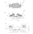
- FIGS. 4A and 4B are a schematic plan view and a cross-sectional view of the TFT 101 of the first embodiment, respectively, and FIG. 4C is an enlarged cross-sectional view of a channel portion of the TFT 101.
- FIG. 5 is a plan view illustrating another TFT 101 in the first embodiment.
- FIG. (A) And (b) is sectional drawing and the top view which show the other example of the protection part 20, respectively.
- (A) And (b) is sectional drawing and a top view which show the further another example of the protection part 20, respectively.
- (A) And (b) is sectional drawing and a top view which show the further another example of the protection part 20, respectively.
- (A) to (e) are schematic plan views illustrating one pixel in the active matrix substrate.
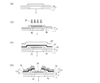
- FIGS. 7A to 7D are schematic process cross-sectional views for explaining an example of a manufacturing method of the TFT 102.
- (A) is a thin film transistor of a reference example
- (b) to (d) are enlarged sectional views schematically showing thin film transistors of comparative examples 1 to 3, respectively.
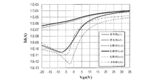
- FIG. 1 It is a figure which shows the VI characteristic of the thin film transistor of a reference example and a comparative example.
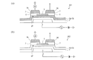
- (A) and (b) are diagrams showing energy band structures in the vicinity of the junction interface between the i-type a-Si layer and the poly-Si layer, respectively.
- (A) And (b) is typical sectional drawing which shows the heterojunction containing TFT801 and the homojunction containing TFT802 which were used for the measurement, respectively.
- the present inventor examined various structures in order to improve the channel mobility of the TFT.
- the polysilicon layer poly-Si layer
- the intrinsic amorphous silicon layer i-type a-Si layer
- this is a heterojunction formed by a poly-Si layer and an i-type a-Si layer.
- HEMT high electron mobility transistor
- 2DEG two-dimensional electron gas
- 2DEG refers to an electron layer (a state in which electrons are distributed two-dimensionally) generated at the interface (region having a thickness of about 10 nm in the vicinity of the interface) when two kinds of semiconductors having different band gap energies are joined.
- 2DEG is known to be produced from compound semiconductors such as GaAs, InP, GaN, and SiGe, but a poly-Si layer and other semiconductor layers having a larger band gap energy than poly-Si. It has not been known that 2DEG can occur at the joint interface with (for example, i-type a-Si layer).
- a junction between two semiconductor layers having different band gap energies is a “semiconductor heterojunction”, and two semiconductors having the same band gap energy.
- a layer junction (for example, a junction between an i-type a-Si layer and an n + -type a-Si layer) is referred to as a “semiconductor homojunction”.
- FIG. 12A and 12B are schematic diagrams for explaining an example of the energy band structure in the vicinity of the interface of the semiconductor heterojunction.
- a semiconductor heterojunction formed by disposing an i-type a-Si layer on a non-doped poly-Si layer (active layer) in a bottom gate type polycrystalline silicon TFT is shown.
- FIG. 12A illustrates an energy band structure in a state where no gate voltage is applied
- FIG. 12B illustrates an energy band structure in a state where a positive voltage is applied to a gate electrode (not shown).
- the band gap energy Eg1 of the poly-Si layer is about 1.1 eV, and the band gap energy Eg2 of the i-type a-Si layer is about 1.88 eV.
- a depletion layer is formed on the side of the poly-Si layer.
- the flow of electrons is indicated by an arrow 91, and the flow of holes is indicated by an arrow 92.
- a quantum well qw is formed at the interface between the i-type a-Si layer and the poly-Si layer, and 2DEG is generated by accumulating electrons.
- the region where 2DEG is generated (hereinafter referred to as “2DEG region”) may have a higher mobility than the poly-Si layer. Therefore, it is possible to increase the channel mobility of the TFT by forming a semiconductor heterojunction in the channel portion of the TFT and generating a 2DEG region with high mobility.
- the mobility of a portion that becomes a channel in the active layer of the TFT is referred to as “channel mobility” and is distinguished from the mobility of the material of the active layer itself.
- the poly-Si layer of the semiconductor heterojunction needs to be positioned closer to the gate electrode than the i-type a-Si layer.
- a (non-doped) polysilicon layer that does not contain an impurity imparting conductivity type as the poly-Si layer. Note that the Fermi level before joining the poly-Si layer and the i-type a-Si layer only needs to have such a relationship that the quantum well qw described above is formed by the joining, and in a range satisfying the relationship.
- the poly-Si layer may contain impurities.
- the junction interface between the i-type a-Si layer and the poly-Si layer has been described as an example.
- a layer made of an intrinsic semiconductor other than a-Si i-type semiconductor layer
- a poly-Si layer a similar 2DEG region may also occur at the bonding interface.
- the i-type semiconductor layer only needs to have a Fermi level (Fermi level before junction) in which the above-described quantum well qw is formed in the vicinity of the junction interface with the poly-Si layer.
- It may be a layer made of a wide band gap semiconductor such as a semiconductor (eg, an In—Ga—Zn—O-based semiconductor).
- FIGS. 13A and 13B are schematic cross-sectional views showing ES type TFTs 801 and 802 used for capacitance measurement, respectively.
- the TFT 801 is a TFT having a semiconductor heterojunction between a gate and a source / drain (referred to as a “heterojunction-containing TFT”)
- the TFT 802 is a TFT having a semiconductor homojunction between a gate and a source / drain (“homojunction”). It is referred to as “containing TFT”.
- the heterojunction-containing TFT 801 includes a gate electrode 2 formed on a substrate, a gate insulating layer 3 covering the gate electrode 2, a semiconductor layer (active layer) 4 formed on the gate insulating layer 3, and a semiconductor layer 4 , A protective insulating layer (etch stop layer) 5 covering the channel region, and a source electrode 8s and a drain electrode 8d.
- the semiconductor layer 4 is a polysilicon layer (poly-Si layer). An i-type a made of intrinsic amorphous silicon is used as a contact layer between the semiconductor layer 4 and the protective insulating layer 5 and the source electrode 8s and between the semiconductor layer 4 and the protective insulating layer 5 and the drain electrode 8d.
- n + -type a-Si layer 7 consisting of -Si layer 6 and the n + -type amorphous silicon are disposed in this order.
- the i-type a-Si layer 6 and the semiconductor layer 4 are in direct contact.
- a junction g1 between the semiconductor layer 4 which is a poly-Si layer and the i-type a-Si layer 6 is a semiconductor heterojunction.
- the homojunction-containing TFT 802 has the same configuration as the heterojunction-containing TFT 801 except that an amorphous silicon layer (a-Si layer) is used as the semiconductor layer 4 and only the n + -type a-Si layer 7 is used as the contact layer.
- a-Si layer amorphous silicon layer
- n + -type a-Si layer 7 is used as the contact layer.
- the junction g2 between the semiconductor layer 4 which is an a-Si layer and the n + -type a-Si layer 7 is a semiconductor homojunction.
- an alternating current (10 kHz) was applied to the heterojunction-containing TFT 801 and the homojunction-containing TFT 802, and the capacitance C between the gate and the source was measured.
- FIG. 14 is a diagram showing the CV characteristics of the heterojunction-containing TFT 801 and the homojunction-containing TFT 802.
- the vertical axis represents the capacitance C
- the horizontal axis represents the gate voltage Vg.
- FIG. 14 shows that the capacitance change of the heterojunction-containing TFT 801 is smaller than that of the homojunction-containing TFT 802. This represents the difference in carrier concentration (electrons).
- carrier concentration electrons
- the higher the carrier concentration the closer the semiconductor is to metal, and thus the smaller the change in capacitance.
- the heterojunction-containing TFT 801 electrons are accumulated in the quantum well qw formed at the interface of the junction g1, and 2DEG is generated, and the carrier concentration is increased as compared with the homojunction-containing TFT 802 by the amount of electrons distributed in 2DEG. Conceivable. This confirms that 2DEG is formed at the interface of the semiconductor heterojunction.
- the heterojunction-containing TFT 801 When a positive voltage is applied to the gate voltage Vg, in the heterojunction-containing TFT 801, electrons accumulated in the quantum well qw at the interface of the junction g1 are expelled to the semiconductor layer 4 side, so that the carrier concentration is homojunction-containing. It is considered to be the same level as the TFT 802.
- the thin film transistor (TFT) of the first embodiment is a polycrystalline silicon TFT.
- the TFT of this embodiment can be applied to circuit substrates such as an active matrix substrate, various display devices such as a liquid crystal display device and an organic EL display device, image sensors, and electronic devices.
- FIG. 1A is a schematic plan view of a thin film transistor (TFT) 101 according to this embodiment
- FIG. 1B is a cross-sectional view of the TFT 101 taken along line I-I ′
- FIG. 1C is an enlarged cross-sectional view of the channel portion of the TFT 101.
- TFT thin film transistor
- the TFT 101 is supported on a substrate 1 such as a glass substrate, and includes a gate electrode 2, a gate insulating layer 3 covering the gate electrode 2, a semiconductor layer (active layer) 4 disposed on the gate insulating layer 3, and a semiconductor.
- a source electrode 8 s and a drain electrode 8 d electrically connected to the layer 4 are provided.
- the semiconductor layer 4 is a layer that functions as an active layer of the TFT 101, and includes a polysilicon region (poly-Si region) 4p. As shown in the drawing, the semiconductor layer 4 may include a poly-Si region 4p and an amorphous silicon region (a-Si region) 4a mainly containing amorphous silicon. Alternatively, the entire semiconductor layer 4 may be a poly-Si region 4p.
- the poly-Si region 4p includes a first region Rs and a second region Rd, and a channel region Rc that is located between them and in which the channel of the TFT 101 is formed.
- the channel region Rc is disposed so as to overlap the gate electrode 2 with the gate insulating layer 3 interposed therebetween.
- the first region Rs is electrically connected to the source electrode 8s, and the second region Rd is electrically connected to the drain electrode 8d.
- protection unit 20 On the channel region Rc of the semiconductor layer 4, a plurality (here, two) of protection units 20 s and 20 d (hereinafter sometimes collectively referred to as “protection unit 20”) are arranged with a space therebetween. Each protection unit 20 is disposed so as to cover a part of the channel region Rc and not cover the first region Rs and the second region Rd. Moreover, each protection part 20 is arrange
- Each protection unit 20 includes an i-type a-Si layer 10 made of amorphous silicon substantially free of impurities (ie, intrinsic), and a protective insulating layer 5 disposed on the i-type a-Si layer 10. It has a laminated structure.
- the i-type a-Si layer 10 is in direct contact with the upper surface of the poly-Si region 4p (channel region Rc).
- the thickness of the i-type a-Si layer 10 may be smaller than the thickness of the protective insulating layer 5.
- the i-type a-Si layer 10 and the protective insulating layer 5 may be patterned using the same mask. In this case, the side surface of the i-type a-Si layer 10 and the side surface of the protective insulating layer 5 are matched.
- the semiconductor layer 4, the protection part 20, the source electrode 8 s and the drain electrode 8 d are covered with an inorganic insulating layer (passivation film) 11.
- the inorganic insulating layer 11 is a portion of the channel region Rc of the semiconductor layer 4 that is not in contact with the protective portion 20 (i-type a-Si layer 10) (in this example, a portion located between the two protective portions 20s and 20d) ) Directly.
- the junction interface between the i-type a-Si layer 10 and the poly-Si region 4p of the semiconductor layer 4 in the protection unit 20 is described above with reference to FIG.
- a 2DEG region 9 in which a two-dimensional electron gas (2DEG) is generated is formed.
- the 2DEG region 9 is, for example, a high mobility region that can have a mobility twice or more that of poly-Si.
- the channel region Rc that is not in contact with the i-type a-Si layer 10 is in contact with, for example, the inorganic insulating layer 11. 2DEG is not generated in this part.
- the region 19 of the semiconductor layer 4 that is not in contact with intrinsic amorphous silicon and in which 2DEG is not formed (or 2DEG is difficult to be formed) is referred to as a “non-2DEG region”.
- the non-2DEG region 19 is located between two adjacent protection portions 20 when viewed from the normal direction of the substrate 1.
- the non-2DEG region 19 is formed so as to divide the 2DEG region 9
- the 2DEG region 9 extends from the first region Rs through the channel region Rc to the second region Rd in the channel length direction. Not formed. That is, the 2DEG region 9 is not formed so as to connect the first region Rs and the second region Rd. Accordingly, it is possible to prevent the source electrode 8s and the drain electrode 8d from being brought into conduction through the 2DEG region 9.
- the poly-Si region 4p that is in contact with the i-type a-Si layer 10 is a non-doped polysilicon region (that is, formed without positively adding n-type impurities). Is preferred.
- the 2DEG region 9 can be reliably formed by the junction interface between the poly-Si region 4p and the i-type a-Si layer 10.
- the first contact layer Cs may be provided between the semiconductor layer 4 and the source electrode 8s, and the second contact layer Cd may be provided between the semiconductor layer 4 and the drain electrode 8d.
- the source electrode 8s is electrically connected to the first region Rs of the semiconductor layer 4 via the first contact layer Cs.
- the drain electrode 8d is electrically connected to the second region Rd of the semiconductor layer 4 through the second contact layer Cd.
- the end portion of the first contact layer Cs and / or the second contact layer Cd may be located on the protection unit 20.
- the protection part (first protection part) 20s is arranged between the first contact layer Cs and the semiconductor layer 4
- the protection part (second protection part) 20d is the second contact layer Cd and the semiconductor layer. 4 is arranged.
- the end portion of the first contact layer Cs is located on the upper surface of the first protective portion 20s
- the end portion of the second contact layer Cd is located on the upper surface of the second protective portion 20d.
- the first contact layer Cs and the second contact layer Cd include an impurity-containing silicon layer (which may be an a-Si layer or a poly-Si layer) containing an impurity imparting conductivity type.
- the impurity-containing silicon layers in the first contact layer Cs and the second contact layer Cd are arranged apart from each other.
- the impurity-containing silicon layer is an n + -type a-Si layer 7 to which an impurity imparting n-type is added.
- the n + type a-Si layer 7 in the first contact layer Cs may be in direct contact with the first region Rs
- the n + type a-Si layer 7 in the second contact layer Cd may be in direct contact with the second region Rd.
- the first contact layer Cs and the second contact layer Cd may have a single layer structure or a laminated structure.
- the first contact layer Cs and the second contact layer Cd may be a single layer of an impurity-containing silicon layer, or may have a stacked structure including an impurity-containing silicon layer as the lowermost layer.
- the impurity-containing silicon layers (here, n + -type a-Si layer 7) of the first contact layer Cs and the second contact layer Cd are in contact with the first region Rs and the second region Rd of the semiconductor layer 4, respectively.
- the first region Rs, the second region Rd, and the n + -type a -Electrons are unlikely to accumulate at the junction with the Si layer 7 and 2DEG is less likely to be generated, so that the occurrence of gate-induced drain leakage (GIDL) due to 2DEG can be suppressed.
- GIDL gate-induced drain leakage
- the 2DEG region 9 having higher mobility than the poly-Si region 4p is disposed in a part of the channel region Rc. Therefore, the channel mobility of the TFT 101 can be improved and the on-current can be increased. Further, since the non-2DEG region 19 is formed so as to divide the 2DEG region 9 in the channel region Rc, the 2DEG region 9 is not formed so as to connect the first region Rs and the second region Rd. For this reason, it is possible to suppress an increase in off-leakage current due to the 2DEG region 9 and a conduction state between the source and the drain, thereby ensuring off characteristics. As described above, according to the present embodiment, the on-characteristic can be improved while maintaining the off-characteristic, so that the on / off ratio can be improved.
- the channel mobility of the TFT 101 can be controlled by using the 2DEG region 9
- variation in characteristics due to variation in crystal grain size in the poly-Si region 4p can be suppressed. Therefore, the reliability of the TFT 101 can be improved.
- the channel region Rc includes a portion in contact with the i-type a-Si layer 10 (a portion where the 2DEG region 9 is formed) and a portion in contact with the inorganic insulating layer 11 (a portion which becomes the non-2DEG region 19).
- the ratio AR of the total area of the portion in contact with the i-type a-Si layer 10 in the channel region Rc to the total area of the channel region Rc is, for example, 20% or more and 90% or less. There may be. If it is 20% or more, the channel mobility can be increased more effectively.
- the ratio AR may be 50% or more. On the other hand, if the ratio AR is 90% or less, an increase in off-leakage current can be more reliably suppressed.
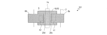
- the structure of the protection unit 20 is not limited to the example shown in FIGS.
- the side surfaces of the protective insulating layer 5 and the i-type a-Si layer 10 may not be aligned.
- the side surfaces of the protective insulating layer 5 and the i-type a-Si layer 10 may be aligned.
- the side surfaces of the protective insulating layer 5 may be located inside or outside. Even in such a case, the 2DEG region 9 can be divided by forming a portion that does not contact the i-type a-Si layer 10 in a part of the channel region Rc. can get.
- the protection unit 20 does not have to be island-shaped.
- the protective insulating layer 5 and the i-type a-Si layer 10 have openings h1 and h2 that expose the first region Rs and the second region Rd of the semiconductor layer 4, respectively. And an opening hs exposing a part of the channel region Rc.
- the opening hs may extend over the channel width.
- the protection parts 20s and 20d are formed on both sides of the opening hs on the channel region Rc.
- the i-type a-Si layer 10 is formed between the protective insulating layer 5 and the semiconductor layer 4, but the i-type a-Si layer 10 is discretely arranged. It may have a structure including a plurality of i-type a-Si islands (hereinafter referred to as “island structure”).
- FIGS. 3A and 3B are a cross-sectional view and a plan view showing another example of the protection unit 20, respectively.
- an i-type a-Si layer 10 having an island-like structure is disposed between the semiconductor layer 4 and the protective insulating layer 5. That is, one or more i-type a-Si islands are formed between the protective insulating layer 5 and the semiconductor layer 4. As illustrated, a plurality of i-type a-Si islands having different sizes (sizes) may be randomly arranged.
- an i-type a-Si layer 10 having an island-like structure as shown in the figure is obtained by forming an intrinsic amorphous silicon film using an initial growth stage by a CVD method. In this case, the area ratio AR can be adjusted by controlling conditions such as the growth time.
- the number and arrangement of the protection units 20 are not limited to the example shown in FIG.
- FIGS. 4 and 5 are diagrams showing still another example of the protection unit 20, in which (a) of each figure is a cross-sectional view and (b) of each figure is a plan view.
- three or more protection units 20 may be arranged at intervals from each other along the channel length direction.
- another protection unit referred to as “central protection unit”
- 20 c may be disposed between the first protection unit 20 s and the second protection unit 20 d.
- the first protection unit 20s may be disposed between the first contact layer Cs and the semiconductor layer 4, and the second protection unit 20d may be disposed between the second contact layer Cd and the semiconductor layer 4.
- the non-2DEG regions 19 are formed between the central protection unit 20c, the first protection unit 20s, and the second protection unit 20d, respectively. Accordingly, in the channel region Rc, the 2DEG region 9 is divided into three by the non-2DEG region 19.
- two or more central protection units 20c may be arranged with a space between the first protection unit 20s and the second protection unit 20d.
- only one protection unit 20 may be arranged on the channel region Rc.
- the protection unit 20 only needs to be spaced from at least one of the first region Rs and the second region Rd (that is, from at least one of the first contact layer Cs and the second contact layer Cd).
- the central protection unit 20c is disposed on the channel region Rc with a space from the first region Rs and the second region Rd.
- a non-2DEG region 19 is formed between the central protection part 20c and the first region Rs and the second region Rd. Accordingly, the 2DEG region 9 is separated from the first region Rs and the second region Rd by the non-2DEG region 19.
- the TFT 101 of this embodiment can be suitably used for an active matrix substrate such as a display device, for example.
- An active matrix substrate (or display device) includes a plurality of source bus lines extending in the column direction, a plurality of gate bus lines extending in the row direction, a display area including a plurality of pixels, and a non-display area (peripheral area) other than the display area Also referred to as a region).
- Each pixel is provided with a pixel TFT as a switching element.
- a drive circuit such as a gate driver may be monolithically formed in the peripheral region.
- the drive circuit includes a plurality of TFTs (referred to as “circuit TFTs”).
- the TFT 101 can be used as a pixel TFT and / or a circuit TFT.
- 6A to 6E are schematic plan views illustrating one pixel on the active matrix substrate.
- a TFT 101 functioning as a pixel TFT and a pixel electrode 13 are arranged.
- the source electrode 8 s of the TFT 101 is electrically connected to one corresponding source bus line SL, and the drain electrode 8 d is electrically connected to the pixel electrode 13.
- the gate electrode 2 is electrically connected to one corresponding gate bus line GL.
- the gate electrode 2 may be a part of the gate bus line GL.
- FIGS. 6A to 6C illustrate pixel structures using the TFT 101 shown in FIGS. 1, 4 and 5 as pixel TFTs, respectively.
- the TFT 101 includes only two of the first protection unit 20s, the second protection unit 20d, and the central protection unit 20c (here, the second protection unit 20d and the central protection unit 20c). You may have.
- FIG. 6E only one of the first protection part 20s, the second protection part 20d, and the central protection part 20c (here, the second protection part 20d) may be included.
- the TFT 101 is arranged so that its channel length is substantially parallel to the row direction (direction in which the gate bus line GL extends), but the channel length is in the column direction (direction in which the source bus line SL extends). ) And may be arranged substantially parallel to each other.
- a liquid crystal display device can be obtained by preparing a counter substrate provided with a counter electrode and a color filter layer, bonding the active matrix substrate and the counter substrate through a sealing material, and injecting liquid crystal between these substrates. .
- various display devices can be obtained by using, as the display medium layer, a material that modulates optical properties or emits light when voltage is applied.
- the active matrix substrate of the present embodiment is also suitably used for display devices such as organic EL display devices and inorganic EL display devices using organic or inorganic fluorescent materials as the display medium layer.
- it can also be suitably used as an active matrix substrate used for X-ray sensors, memory elements, and the like.
- FIG. 7A to 7H are schematic process cross-sectional views for explaining an example of the manufacturing method of the TFT 101.
- FIG. 7A to 7H are schematic process cross-sectional views for explaining an example of the manufacturing method of the TFT 101.
- a gate electrode 2, a gate insulating layer 3, and an a-Si film for active layer 40 are formed in this order on a substrate 1.
- a substrate having an insulating surface such as a glass substrate, a silicon substrate, or a heat-resistant plastic substrate (resin substrate) can be used.
- the gate electrode 2 is formed by forming a gate conductive film on the substrate 1 and patterning it.
- a conductive film for gate (thickness: about 500 nm, for example) is formed on the substrate 1 by sputtering, and the metal film is patterned using a known photolithography process. For example, wet etching is used for etching the gate conductive film.
- the material of the gate electrode 2 is a single metal such as molybdenum (Mo), tungsten (W), copper (Cu), chromium (Cr), tantalum (Ta), aluminum (Al), titanium (Ti), nitrogen, A material containing oxygen or another metal, or a transparent conductive material such as indium tin oxide (ITO) may be used.
- Mo molybdenum
- W tungsten
- Cu copper
- Cr chromium
- Ta tantalum
- Al aluminum
- Ti titanium
- nitrogen A material containing oxygen or another metal, or a transparent conductive material such as indium tin oxide (ITO) may be used.
- the gate insulating layer 3 is formed on the substrate 1 on which the gate electrode 2 is formed by, for example, a plasma CVD method.
- the a-Si film 40 for active layer can be formed by, for example, a CVD method using hydrogen gas (H 2 ) and silane gas (SiH 4 ).
- the active layer a-Si film 40 may be a non-doped amorphous silicon film substantially free of n-type impurities.
- the non-doped amorphous silicon film refers to an a-Si film formed without positively adding n-type impurities (for example, using a source gas not containing n-type impurities).
- the active layer a-Si film 40 may contain an n-type impurity at a relatively low concentration.
- the thickness of the active layer a-Si film 40 may be not less than 20 nm and not more than 70 nm (for example, 50 nm).
- the active layer a-Si film 40 which becomes the channel region of the TFT is irradiated with the laser beam 30.
- an ultraviolet laser such as a XeCl excimer laser (wavelength 308 nm) or a solid laser having a wavelength of 550 nm or less such as a second harmonic (wavelength 532 nm) of a YAG laser can be applied.
- the region irradiated with the laser beam 30 in the active layer a-Si film 40 is heated and melted and solidified to form a poly-Si region 4p.
- the semiconductor layer 4 including the poly-Si region 4p is obtained.
- crystal grains grow in a columnar shape toward the upper surface of the semiconductor layer 4.
- the crystallization method using the laser beam 30 is not particularly limited.
- the laser light 30 from the laser light source is condensed on only a part of the active layer a-Si film 40 via the microlens array, thereby forming the active layer a-Si film 40. It may be partially crystallized.
- this crystallization method is referred to as “partial laser annealing”.
- partial laser annealing When partial laser annealing is used, the time required for crystallization can be greatly shortened compared to conventional laser annealing in which linear laser light is scanned over the entire surface of the a-Si film. It is.
- the microlens array has microlenses arranged in two dimensions or one dimension.
- the laser light 30 is collected by the microlens array and is only applied to a plurality of predetermined regions (irradiation regions) separated from each other in the active layer a-Si film 40.
- Each irradiation region is arranged corresponding to a portion that becomes a channel region of the TFT.
- the position, number, shape, size, etc. of the irradiation area depend on the size of the microlens array (not limited to lenses less than 1 mm), the arrangement pitch, the opening position of the mask arranged on the light source side of the microlens array, etc. Can be controlled.
- the region irradiated with the laser beam 30 in the active layer a-Si film 40 is heated and melted and solidified to become a poly-Si region 4p.
- the region not irradiated with the laser light remains as the a-Si region 4a.
- the a-Si region 4a is disposed, for example, outside the poly-Si region 4p.
- an i-type a-Si film (referred to as “2DEG forming a-Si film”) 100 is formed on the semiconductor layer 4.
- the 2DEG forming a-Si film 100 is formed by, for example, a CVD method.
- the thickness of the 2DEG forming a-Si film 100 may be, for example, not less than 5 nm and not more than 50 nm. If the thickness is 5 nm or more, a 2DEG region can be reliably generated between the 2DEG forming a-Si film 100 and the poly-Si region 4p.
- the a-Si film 100 for forming 2DEG can be formed using an initial growth stage by a CVD method. Thereby, a desired thin 2DEG forming a-Si film 100 can be easily formed.
- the deposition time of the 2DEG forming a-Si film 100 by the CVD method is not particularly limited, but may be, for example, 2 seconds to 150 seconds.
- a 2DEG forming a-Si film (thickness: 2 nm or more and 5 nm or less) 100 having an island structure may be formed by controlling film formation conditions such as deposition time.
- the deposition time at this time is not particularly limited, but may be, for example, 0.2 seconds or more and 1.0 seconds or less. If it is 1.0 second or less, the 2DEG forming a-Si film 100 can be more reliably deposited in an island shape. If it is 0.2 seconds or longer, the 2DEG region 9 can be more reliably formed between the 2DEG forming a-Si film 100 and the poly-Si region 4p.
- the size of each island, the formation position, the number in one channel region Rc, etc. are random. Become. Accordingly, the 2DEG regions 9 are also randomly formed (see FIG. 3).
- the method for forming the 2DEG forming a-Si film 100 is not limited to the CVD method, and other known methods may be used.
- a protective insulating film 50 serving as a protective insulating layer (etch stop layer) is formed on the semiconductor layer 4.
- a silicon oxide film (SiO 2 film) is formed as the protective insulating film 50 by a CVD method.
- the thickness of the protective insulating film 50 may be, for example, 30 nm or more and 300 nm or less.
- dehydrogenation annealing treatment for example, 450 ° C., 60 minutes
- each protection unit 20 includes a protective insulating layer 5 formed from the protective insulating film 50 and an i-type a-Si layer 10 formed from the 2DEG forming a-Si film 100. Part of the poly-Si region 4p (portion serving as a contact region) is exposed from the protection portion 20 on the source side and drain side of the portion serving as the channel region.
- the first protection unit 20s and the second protection unit 20d are arranged on the channel region Rc with an interval therebetween.
- a portion of the poly-Si region 4p located between the protective portions 20s and 20d is exposed.
- a contact layer Si film 70 is formed so as to cover the semiconductor layer 4 and the protection unit 20.
- an n + -type a-Si film (thickness: for example, about 0.05 ⁇ m) 70 containing an n-type impurity (here, phosphorus) is deposited by plasma CVD.
- the concentration of the n-type impurity is, for example, 1 ⁇ 10 18 cm ⁇ 3 or more and 5 ⁇ 10 20 cm ⁇ 3 or less.
- a mixed gas of silane, hydrogen, and phosphine (PH 3 ) is used as a source gas.
- an i-type a-Si film (thickness: about 0.1 ⁇ m, for example) and an n + -type a-Si containing an n-type impurity (for example, phosphorus) are formed by plasma CVD.
- a laminated film including a film may be formed.
- Hydrogen gas and silane gas are used as the source gas for the i-type a-Si film.
- a source gas for the n + -type a-Si film a mixed gas of silane, hydrogen, and phosphine (PH 3 ) is used.
- a conductive film (thickness: about 0.3 ⁇ m, for example) for the source and drain electrodes and a resist mask M are formed on the Si film for contact layer (here, n + -type a-Si film 70).
- the source and drain electrode conductive films can be formed using the same material as the gate conductive film and in the same manner as the gate conductive film.
- the conductive film for the source and drain electrodes and the n + -type a-Si film 70 are patterned by dry etching, for example.
- the source electrode 8s and the drain electrode 8d are formed from the conductive film (source / drain separation step).
- the first contact layer Cs and the second contact layer Cd are formed apart from the n + -type a-Si film 70.
- the protective insulating layer 5 functions as an etch stop, a portion of the semiconductor layer 4 covered with the protective insulating layer 5 (protective portion 20) is not etched.
- the channel-side end portions of the first contact layer Cs and the second contact layer Cd may be located on the upper surface of the protective insulating layer 5.
- the surface layer of the portion of the semiconductor layer 4 that is not covered with the protective portion 20 (for example, the portion located between the first protective portion 20s and the second protective portion 20d) is removed by etching. In some cases (overetching). Thereafter, the resist mask M is peeled from the substrate 1. In this way, the TFT 101 is manufactured.
- a hydrogen plasma treatment may be performed on the poly-Si region 4p after the source / drain separation step.
- an interlayer insulating layer is formed so as to cover the TFT 101 as shown in FIG.
- an inorganic insulating layer (passivation film) 11 and an organic insulating layer 12 are formed as interlayer insulating layers.
- the inorganic insulating layer 11 a silicon oxide layer, a silicon nitride layer, or the like may be used.
- a SiNx layer thickness: about 200 nm, for example
- the inorganic insulating layer 11 is in contact with the protective insulating layer 5 between the source electrode 8s and the drain electrode 8d (gap).
- the organic insulating layer 12 may be, for example, an organic insulating film (thickness: 1 to 3 ⁇ m, for example) containing a photosensitive resin material. Thereafter, the organic insulating layer 12 is patterned to form an opening. Subsequently, the inorganic insulating layer 11 is etched (dry etching) using the organic insulating layer 12 as a mask. Thereby, a contact hole CH reaching the drain electrode 8 d is formed in the inorganic insulating layer 11 and the organic insulating layer 12.
- a transparent conductive film is formed on the organic insulating layer 12 and in the contact hole CH.
- metal oxides such as indium-tin oxide (ITO), indium-zinc oxide, and ZnO can be used.
- ITO indium-tin oxide
- ZnO zinc-nitride
- an indium-zinc oxide film is formed as the transparent conductive film by sputtering.
- the transparent conductive film is patterned by wet etching, for example, and the pixel electrode 13 is obtained.
- the pixel electrode 13 is spaced apart for each pixel.
- Each pixel electrode 13 is in contact with the drain electrode 8d of the corresponding TFT in the contact hole.
- the source electrode 8s of the TFT 101 is electrically connected to a source bus line (not shown), and the gate electrode 2 is electrically connected to a gate bus line (not shown).
- the semiconductor layer 4, the first contact layer Cs, and the second contact layer Cd may each be patterned in an island shape in a region where the TFT 101 is formed (TFT formation region).
- the semiconductor layer 4, the first contact layer Cs, and the second contact layer Cd may be extended to a region other than the region where the TFT 101 is formed (TFT formation region).
- the semiconductor layer 4 may extend so as to overlap a source bus line connected to the source electrode 8s.
- the portion of the semiconductor layer 4 that is located in the TFT formation region only needs to include the poly-Si region 4p, and the portion that extends to the region other than the TFT formation region may be the a-Si region 4a.
- the method for crystallizing the a-Si film 40 for the active layer is not limited to the partial laser annealing described above. A part or all of the active layer a-Si film 40 may be crystallized by using another known method.
- a semiconductor layer made of another intrinsic semiconductor (which may be amorphous or crystalline) may be used instead of the i-type a-Si layer 10.
- the i-type semiconductor layer has a larger band gap than the poly-Si region 4p, and forms a semiconductor heterojunction with the poly-Si region 4p.
- a semiconductor layer formed of a wide band gap semiconductor such as an intrinsic oxide semiconductor (eg, an In—Ga—Zn—O-based semiconductor) can be used.
- the i-type semiconductor layer has a Fermi level (Fermi level before junction) such that the quantum well qw described above is formed in the vicinity of the junction interface with the poly-Si region 4p.
- the i-type semiconductor layer can be formed by a process similar to that of the i-type a-Si layer 10, for example.
- the i-type semiconductor layer may include a plurality of discrete i-type semiconductor islands (see FIG. 3).
- the oxide semiconductor may be amorphous or crystalline.
- the crystalline oxide semiconductor may be, for example, a polycrystalline oxide semiconductor, a microcrystalline oxide semiconductor, or a crystalline oxide semiconductor in which the c-axis is oriented substantially perpendicular to the layer surface.
- the material, structure, film forming method, and the like of the amorphous or crystalline oxide semiconductor are described in, for example, Japanese Patent No. 6275294. For reference, the entire disclosure of Japanese Patent No. 6275294 is incorporated herein by reference.
- the TFT of the reference embodiment is a channel etch (CE) type polycrystalline silicon TFT.
- FIG. 8A is a schematic plan view of a thin film transistor (TFT) 102 according to a reference embodiment
- FIG. 8B is a cross-sectional view of the TFT 102 taken along the line II-II ′.
- FIG. 8C is an enlarged cross-sectional view of the channel portion of the TFT 102.
- TFT thin film transistor
- a protective part (protective part 20 shown in FIG. 1) including an etch stop layer covering the channel region Rc is not provided between the semiconductor layer 4 and the source electrode 8s and the drain electrode 8d.
- the TFT 102 in the channel region Rc, at least one i-type a-Si island 6a is disposed on the poly-Si region 4p, and the i-type a-Si island 6a and A 2DEG region 9 is formed between the poly-Si region 4p.
- the inorganic insulating layer 11 is in direct contact with the i-type a-Si island 6a and the portion of the semiconductor layer 4 that is not covered with the i-type a-Si island 6a between the source electrode 8s and the drain electrode 8d. Yes.
- Other structures may be the same as those of the TFT 101 shown in FIG.
- the first contact layer Cs and the second contact layer Cd include, for example, an i-type a-Si layer 6 in direct contact with the semiconductor layer 4 and an n + -type a disposed on the i-type a-Si layer 6. It may have a stacked structure including a -Si layer.
- the i-type a-Si island 6a can be formed using the same silicon film as the i-type a-Si layer 6.
- the i-type a-Si island 6a can be formed by performing etching under conditions such that the i-type a-Si layer 6 remains partially on the channel region Rc.
- the i-type a-Si island 6a is thinner than the i-type a-Si layer 6 of the first contact layer Cs and the second contact layer Cd.
- a plurality of i-type a-Si islands 6a having different sizes may be randomly arranged on the channel region Rc.
- FIGS. 9A to 9D are process cross-sectional views for explaining an example of the manufacturing method of the TFT 102.
- FIGS. 9A to 9D are process cross-sectional views for explaining an example of the manufacturing method of the TFT 102.
- FIGS. 9A to 9D are process cross-sectional views for explaining an example of the manufacturing method of the TFT 102.
- FIG. 3 differences from the above-described embodiment (FIG. 3) will be mainly described.
- the description of the material, thickness, formation method, and the like of each layer will be omitted as appropriate in the same manner as in the above-described embodiment.
- a gate electrode 2, a gate insulating layer 3, and an a-Si film for active layer 40 are formed on a substrate 1.
- the semiconductor layer 4 including the poly-Si region 4p is obtained by irradiating the active layer a-Si film 40 with the laser beam 30.
- the semiconductor layer 4 including the poly-Si region 4p and the a-Si region 4a may be formed by partial laser annealing.
- a Si film for contact layer and a conductive film 80 for source / drain electrodes are formed in this order so as to cover the semiconductor layer 4.
- a Si film for the contact layer an i-type a-Si film (thickness: about 0.1 ⁇ m, for example) 60 and an n + -type a ⁇ containing an n-type impurity (for example, phosphorus) are formed by plasma CVD.
- a laminated film including a Si film (thickness: about 0.05 ⁇ m, for example) 70 is formed. Hydrogen gas and silane gas are used as source gases for the i-type a-Si film 60.
- n + -type a-Si film 70 As a source gas for the n + -type a-Si film 70, a mixed gas of silane, hydrogen and phosphine (PH 3 ) is used.
- the phosphorus concentration of the n + -type a-Si film 70 may be, for example, 1 ⁇ 10 18 cm ⁇ 3 or more and 5 ⁇ 10 20 cm ⁇ 3 or less.
- the i-type a-Si film 60, the n + -type a-Si film 70, and the conductive film 80 are patterned by, for example, dry etching using a resist mask (not shown). (Source / drain separation step). At this time, in the region not covered with the resist mask (region serving as the channel region), the conductive film 80 and the n + -type a-Si film 70 are completely removed, and the i-type a-Si film 60 is a semiconductor layer. The patterning is performed under the condition that the island 4 remains on the island 4.
- the i-type a-Si layer 6 can be left in an island shape on the channel region.
- the first contact layer Cs and the second contact layer Cd are obtained from the i-type a-Si film 60 and the n + -type a-Si film 70, and the source electrode 8 s and the drain electrode 8 d are formed from the conductive film 80. can get.
- an i-type a-Si island 6 a can be formed from the i-type a-Si film 60.
- the patterning may be performed under the condition that only the surface portion of the i-type a-Si film 60 that is not covered with the resist mask is removed (thinned).
- the i-type a-Si island 6a may be formed by separately patterning the thinned i-type a-Si film 60 into an island shape.
- the i-type a-Si island 6a can be formed in a predetermined pattern.
- an i-type a-Si island 6a may be disposed as shown in FIGS.
- another i-type a-Si film may be formed so as to cover the channel region, and patterning may be performed to form the i-type a-Si island 6a.
- the i-type a-Si film 60 may not be used as the Si film for the contact layer.
- FIG. 10A is a schematic enlarged cross-sectional view of the thin film transistor of the reference example
- FIGS. 10B to 10D are schematic enlarged cross-sectional views of the thin film transistors of Comparative Examples 1 to 3, respectively.
- reference thin film transistors s1 and s2 were manufactured by the method described above with reference to FIG.
- the thin film transistors s1 and s2 have the same structure as that in FIG.
- the thin film transistors of Comparative Examples 1 and 2 were produced in the same manner as in the Reference Example except for the etching conditions (for example, etching time) in the source / drain separation step.
- the etching conditions for example, etching time
- Comparative Example 1 only the surface portion of the i-type a-Si layer 6 is removed between the source electrode 8s and the drain electrode 8d, and the i-type a-Si layer 6 is formed so as to cover substantially the entire channel region Rc. Etching was performed under the remaining conditions to obtain thin film transistors s3 and s4.
- Comparative Example 2 the i-type a-Si layer 6 is completely removed between the source electrode 8s and the drain electrode 8d, and the surface portion of the semiconductor layer 4 is over-etched. s5 was obtained.
- the source / drain separation process was performed in a state where the channel region Rc was covered with the protective insulating layer (SiO 2 layer) 5 to fabricate an ES type thin film transistor s6.
- the protective insulating layer 5 and the channel region Rc are in direct contact with each other, and no a-Si island is provided between them.
- FIG. 11 is a diagram showing the VI (gate voltage Vgs-drain current Id) characteristics of the thin film transistors of the reference example and comparative examples 1 to 3.
- the on-current of the thin film transistor s5 of Comparative Example 2 is lower than that of the thin film transistors s1 and s2 of the reference example. This is considered because the i-type a-Si layer 6 does not remain on the channel region, so that 2DEG is not generated and the high mobility effect by 2DEG is not obtained.
- the on-current of the thin film transistor s5 of Comparative Example 2 is lower than that of the thin film transistor s6 of Comparative Example 3.
- the reason for this is that in the thin film transistor s5, the surface portion of the semiconductor layer 4 is over-etched and the polycrystalline silicon layer is largely removed, most of which becomes a small crystal grain size layer and an amorphous layer, or the channel portion is damaged.
- the on-current is considered to be lower than that of the thin film transistor s6 in which the surface of the semiconductor layer 4 is protected.
- the thin film transistors s1 and s2 of the reference example higher on-currents can be obtained than the thin film transistors s5 and s6 of the comparative example 2 and the comparative example 3.
- the high mobility 2DEG region 9 is formed at the junction between the channel region Rc and the i-type a-Si island 6a, which is considered to increase the channel mobility of the TFT. . Further, a portion of the channel region Rc that is not in contact with the i-type a-Si island 6a becomes a non-2DEG region where no 2DEG is formed.
- the 2DEG region 9 is not formed from the first region Rs to the second region Rd in the channel length direction (so as to connect the source and the drain). It is considered that the occurrence of punch-through was suppressed.
- the 2DEG region 9 is generated in the channel region Rc, and the non-DEG region is arranged so that the source and drain are not connected via the 2DEG region 9, thereby It is confirmed that the on-current can be improved while securing the above.
- a CE type TFT has been described as an example of the thin film transistor of the reference example, but the 2DEG region and the non-2DEG region are formed in the channel region Rc even in the TFT of the embodiment shown in FIG. Therefore, the same effect as described above can be obtained.
- the structure of the TFT of the present invention is not limited to the structure described above with reference to FIG.
- the TFT according to the embodiment of the present invention only needs to have a structure in which a silicon heterojunction is formed in a channel portion and an on-current can be increased using the 2DEG region 9 generated at the junction interface.
- Embodiments of the present invention can be widely applied to devices and electronic devices having TFTs.
- circuit boards such as active matrix substrates, liquid crystal display devices, display devices such as organic electroluminescence (EL) display devices and inorganic electroluminescence display devices, imaging devices such as radiation detectors and image sensors, image input devices,
- EL organic electroluminescence
- imaging devices such as radiation detectors and image sensors
- the present invention can be applied to an electronic device such as a fingerprint reading device.
Landscapes
- Thin Film Transistor (AREA)
- Chemical & Material Sciences (AREA)
- Engineering & Computer Science (AREA)
- Crystallography & Structural Chemistry (AREA)
- Microelectronics & Electronic Packaging (AREA)
Abstract
L'invention concerne un transistor à couches minces (101) comprenant : une électrode de grille (2) qui est supportée par un substrat (1) ; une couche d'isolation de grille (3) qui recouvre l'électrode de grille ; une couche semi-conductrice (4) qui est positionnée sur la couche d'isolation de grille et comprend une région de polysilicium (4p), ladite région de polysilicium (4p) comprenant une première région (Rs), une seconde région (Rd), et une région de canal (Rc) qui est située entre la première région et la seconde région ; une électrode de source (8s) qui est connectée électriquement à la première région ; une électrode de drain (8d) qui est électriquement connectée à la seconde région ; et au moins une section de protection (20) qui est positionnée sur une section de la région de canal, séparée par un espace à partir de la première région et/ou de la seconde région, la section de protection (20) est positionnée de façon à entrer directement en contact avec la région de canal (Rc), et a une structure en couches comprenant un îlot de semi-conducteur de type i (10) qui comprend un semi-conducteur intrinsèque et a une bande interdite plus grande que la région de polysilicium, et une couche d'isolation protectrice (5) qui est positionnée sur la couche semi-conductrice de type i.
Priority Applications (3)
| Application Number | Priority Date | Filing Date | Title |
|---|---|---|---|
| CN201880094361.3A CN112236868A (zh) | 2018-06-07 | 2018-06-07 | 薄膜晶体管及其制造方法 |
| US15/734,937 US20210234049A1 (en) | 2018-06-07 | 2018-06-07 | Thin-film transistor and manufacturing method therefor |
| PCT/JP2018/021922 WO2019234893A1 (fr) | 2018-06-07 | 2018-06-07 | Transistor à couches minces et son procédé de fabrication |
Applications Claiming Priority (1)
| Application Number | Priority Date | Filing Date | Title |
|---|---|---|---|
| PCT/JP2018/021922 WO2019234893A1 (fr) | 2018-06-07 | 2018-06-07 | Transistor à couches minces et son procédé de fabrication |
Publications (1)
| Publication Number | Publication Date |
|---|---|
| WO2019234893A1 true WO2019234893A1 (fr) | 2019-12-12 |
Family
ID=68769830
Family Applications (1)
| Application Number | Title | Priority Date | Filing Date |
|---|---|---|---|
| PCT/JP2018/021922 Ceased WO2019234893A1 (fr) | 2018-06-07 | 2018-06-07 | Transistor à couches minces et son procédé de fabrication |
Country Status (3)
| Country | Link |
|---|---|
| US (1) | US20210234049A1 (fr) |
| CN (1) | CN112236868A (fr) |
| WO (1) | WO2019234893A1 (fr) |
Families Citing this family (2)
| Publication number | Priority date | Publication date | Assignee | Title |
|---|---|---|---|---|
| CN114068722A (zh) * | 2020-08-04 | 2022-02-18 | 京东方科技集团股份有限公司 | 薄膜晶体管及其制备方法、显示装置 |
| CN118335789B (zh) | 2024-06-12 | 2024-10-01 | 南京大学 | 用于辐照损伤检测的GaN HEMT器件及其检测和制作方法 |
Citations (4)
| Publication number | Priority date | Publication date | Assignee | Title |
|---|---|---|---|---|
| WO2010147032A1 (fr) * | 2009-06-18 | 2010-12-23 | シャープ株式会社 | Dispositif à semi-conducteurs |
| JP2010287618A (ja) * | 2009-06-09 | 2010-12-24 | Mitsubishi Electric Corp | 薄膜トランジスタ及びその製造方法、並びに薄膜トランジスタアレイ基板及び表示装置 |
| WO2013118233A1 (fr) * | 2012-02-06 | 2013-08-15 | パナソニック株式会社 | Procédé de fabrication d'un dispositif à semiconducteur à film mince et dispositif à semiconducteur à film mince |
| WO2017187486A1 (fr) * | 2016-04-25 | 2017-11-02 | 堺ディスプレイプロダクト株式会社 | Transistor à couche mince, dispositif d'affichage, et procédé de fabrication de transistor à couche mince |
Family Cites Families (3)
| Publication number | Priority date | Publication date | Assignee | Title |
|---|---|---|---|---|
| JPH0671083B2 (ja) * | 1986-06-16 | 1994-09-07 | 株式会社日立製作所 | 薄膜半導体装置 |
| KR100785020B1 (ko) * | 2006-06-09 | 2007-12-12 | 삼성전자주식회사 | 하부 게이트 박막 트랜지스터 및 그 제조방법 |
| CN103053026A (zh) * | 2011-08-10 | 2013-04-17 | 松下电器产业株式会社 | 薄膜晶体管器件以及薄膜晶体管器件的制造方法 |
-
2018
- 2018-06-07 WO PCT/JP2018/021922 patent/WO2019234893A1/fr not_active Ceased
- 2018-06-07 CN CN201880094361.3A patent/CN112236868A/zh active Pending
- 2018-06-07 US US15/734,937 patent/US20210234049A1/en not_active Abandoned
Patent Citations (4)
| Publication number | Priority date | Publication date | Assignee | Title |
|---|---|---|---|---|
| JP2010287618A (ja) * | 2009-06-09 | 2010-12-24 | Mitsubishi Electric Corp | 薄膜トランジスタ及びその製造方法、並びに薄膜トランジスタアレイ基板及び表示装置 |
| WO2010147032A1 (fr) * | 2009-06-18 | 2010-12-23 | シャープ株式会社 | Dispositif à semi-conducteurs |
| WO2013118233A1 (fr) * | 2012-02-06 | 2013-08-15 | パナソニック株式会社 | Procédé de fabrication d'un dispositif à semiconducteur à film mince et dispositif à semiconducteur à film mince |
| WO2017187486A1 (fr) * | 2016-04-25 | 2017-11-02 | 堺ディスプレイプロダクト株式会社 | Transistor à couche mince, dispositif d'affichage, et procédé de fabrication de transistor à couche mince |
Also Published As
| Publication number | Publication date |
|---|---|
| US20210234049A1 (en) | 2021-07-29 |
| CN112236868A (zh) | 2021-01-15 |
Similar Documents
| Publication | Publication Date | Title |
|---|---|---|
| JP5301971B2 (ja) | 薄膜トランジスタ、その製造方法、及びこれを含む有機電界発光表示装置 | |
| CN110660867B (zh) | 薄膜晶体管、显示装置和薄膜晶体管的制造方法 | |
| US9023685B2 (en) | Semiconductor device, fabrication method for the same, and display apparatus | |
| CN112740420B (zh) | 薄膜晶体管及其制造方法 | |
| US20210343878A1 (en) | Thin-film transistor and method for manufacturing same | |
| US20190243194A1 (en) | Active matrix substrate and method for manufacturing same | |
| US20190296050A1 (en) | Active matrix substrate and method for manufacturing same | |
| US8310611B2 (en) | Display device and manufacturing method thereof | |
| US11476282B2 (en) | Active matrix substrate and method for manufacturing same | |
| WO2019234892A1 (fr) | Transistor à couches minces et son procédé de fabrication | |
| KR101761634B1 (ko) | 박막 트랜지스터 기판 및 이의 제조 방법 | |
| WO2019234893A1 (fr) | Transistor à couches minces et son procédé de fabrication | |
| JP2010287645A (ja) | 薄膜トランジスタおよびその製造方法 | |
| WO2019234890A1 (fr) | Transistor à couches minces et son procédé de fabrication | |
| US11502115B2 (en) | Active matrix substrate and method for manufacturing same | |
| WO2019234891A1 (fr) | Transistor à couches minces et procédé de fabrication associé | |
| US20210036163A1 (en) | Thin film transistor and production method therefor | |
| JP2009272534A (ja) | 半導体装置、表示装置及び集積回路 | |
| WO2020084708A1 (fr) | Transistor à couches minces et son procédé de fabrication | |
| CN103003947A (zh) | 显示装置、用于显示装置中的薄膜晶体管、及薄膜晶体管的制造方法 | |
| US11121262B2 (en) | Semiconductor device including thin film transistor and method for manufacturing the same | |
| US11081507B2 (en) | Semiconductor device and method for manufacturing same | |
| JP2009147153A (ja) | 薄膜トランジスタ構造、表示装置及びその製造方法 |
Legal Events
| Date | Code | Title | Description |
|---|---|---|---|
| 121 | Ep: the epo has been informed by wipo that ep was designated in this application |
Ref document number: 18922021 Country of ref document: EP Kind code of ref document: A1 |
|
| NENP | Non-entry into the national phase |
Ref country code: DE |
|
| 122 | Ep: pct application non-entry in european phase |
Ref document number: 18922021 Country of ref document: EP Kind code of ref document: A1 |
|
| NENP | Non-entry into the national phase |
Ref country code: JP |