WO2019237366A1 - Circuit d'étalonnage de facteur de marche d'horloge de référence - Google Patents
Circuit d'étalonnage de facteur de marche d'horloge de référence Download PDFInfo
- Publication number
- WO2019237366A1 WO2019237366A1 PCT/CN2018/091691 CN2018091691W WO2019237366A1 WO 2019237366 A1 WO2019237366 A1 WO 2019237366A1 CN 2018091691 W CN2018091691 W CN 2018091691W WO 2019237366 A1 WO2019237366 A1 WO 2019237366A1
- Authority
- WO
- WIPO (PCT)
- Prior art keywords
- duty cycle
- circuit
- reference clock
- clock signal
- detection circuit
- Prior art date
- Legal status (The legal status is an assumption and is not a legal conclusion. Google has not performed a legal analysis and makes no representation as to the accuracy of the status listed.)
- Ceased
Links
Images


Classifications
-
- H—ELECTRICITY
- H03—ELECTRONIC CIRCUITRY
- H03K—PULSE TECHNIQUE
- H03K5/00—Manipulating of pulses not covered by one of the other main groups of this subclass
- H03K5/156—Arrangements in which a continuous pulse train is transformed into a train having a desired pattern
- H03K5/1565—Arrangements in which a continuous pulse train is transformed into a train having a desired pattern the output pulses having a constant duty cycle
-
- Y—GENERAL TAGGING OF NEW TECHNOLOGICAL DEVELOPMENTS; GENERAL TAGGING OF CROSS-SECTIONAL TECHNOLOGIES SPANNING OVER SEVERAL SECTIONS OF THE IPC; TECHNICAL SUBJECTS COVERED BY FORMER USPC CROSS-REFERENCE ART COLLECTIONS [XRACs] AND DIGESTS
- Y02—TECHNOLOGIES OR APPLICATIONS FOR MITIGATION OR ADAPTATION AGAINST CLIMATE CHANGE
- Y02B—CLIMATE CHANGE MITIGATION TECHNOLOGIES RELATED TO BUILDINGS, e.g. HOUSING, HOUSE APPLIANCES OR RELATED END-USER APPLICATIONS
- Y02B70/00—Technologies for an efficient end-user side electric power management and consumption
- Y02B70/10—Technologies improving the efficiency by using switched-mode power supplies [SMPS], i.e. efficient power electronics conversion e.g. power factor correction or reduction of losses in power supplies or efficient standby modes
Definitions
- the present application relates to the field of circuits, and in particular, to a reference clock duty cycle calibration circuit.
- wireless communication technologies dominate, such as terminal wireless communications, short-range wireless communications, and large public network wireless communications.
- terminal wireless communications short-range wireless communications
- large public network wireless communications With the development of wireless communication, the requirements for the quality and speed of data transmission are getting higher and higher.
- the embodiment of the invention discloses a reference clock duty cycle calibration circuit, which can effectively improve the noise of the reference clock and improve the communication performance.
- an embodiment of the present invention provides a reference clock duty cycle calibration circuit, including: a first low-noise low-dropout voltage regulator for providing a low-noise voltage; and an oscillating circuit for the low-noise voltage Driven by a sine wave signal, a duty cycle adjustment circuit is configured to adjust the duty cycle of the first reference clock signal according to the first reference voltage and the sine wave signal.
- the duty cycle calibration circuit includes: Ratio detection circuit, configured to detect the duty cycle of the first reference clock signal, and adjust the amplitude of the output signal of the duty cycle detection circuit according to the duty cycle of the first reference clock signal; the second low noise
- the low-dropout voltage regulator is configured to adjust and output the first reference voltage according to the amplitude of the output signal of the duty cycle detection circuit.
- the amplitude is directly proportional.
- the sine wave signal generated by the low-noise voltage-driven oscillation circuit has low-noise characteristics, so that the signal output by the reference clock duty cycle calibration circuit also has low-noise characteristics, which effectively improves the noise of the reference clock and improves communication performance.
- the sine wave signal generated by the oscillating circuit is input to the duty cycle adjusting circuit in a DC coupling manner.
- adjusting the duty cycle of the output signal of the duty cycle detection circuit according to the duty cycle of the first reference clock signal by the duty cycle detection circuit includes:
- the duty cycle detection circuit is configured to detect whether the duty cycle of the first reference clock signal deviates from a preset duty cycle
- the duty cycle detection circuit is further configured to adjust an amplitude of an output signal of the duty cycle detection circuit when it is determined that the duty cycle of the first reference clock signal deviates from a preset duty cycle; When the duty cycle of the first reference clock signal does not deviate from the preset duty cycle, the amplitude of the output signal of the duty cycle detection circuit is not adjusted.
- the duty cycle detection circuit is configured to adjust the amplitude of an output signal of the duty cycle detection circuit when the duty cycle of the first reference clock signal deviates from a preset duty cycle. Values, including:
- the duty ratio detection circuit When it is detected that the duty ratio of the first reference clock signal is greater than the preset duty ratio for N consecutive times, the duty ratio detection circuit increases the amplitude of its output signal, where N is greater than 1. Integer
- the duty ratio detection circuit When it is detected that the duty ratio of the first reference clock signal is less than the preset duty ratio for M consecutive times, the duty ratio detection circuit reduces the amplitude of its output signal, where M is greater than 1. Integer. Because the first reference voltage value is proportional to the amplitude of the output signal of the duty cycle detection circuit, the first reference voltage can be adjusted by adjusting the amplitude of the output signal of the duty cycle detection circuit, and the duty cycle adjustment circuit can be implemented. The duty cycle of the first reference clock signal is adjusted, thereby achieving dynamic adjustment of the duty cycle of the output signal of the reference clock duty cycle calibration circuit.
- the obtaining the duty cycle of the first reference clock signal by the duty cycle detecting circuit includes:
- the duty cycle detection circuit is configured to obtain a high-level duration or a low-level duration of the first reference clock signal
- the duty cycle detection circuit is configured to determine a duty cycle of the first reference clock signal according to a period of the first reference clock signal and a high-level duration or a low-level duration of the first reference clock signal. .
- the preset duty cycle is 50%.
- the duty cycle calibration circuit further includes:
- a digital-to-analog conversion circuit configured to convert an output signal of the duty cycle detection circuit into a second reference voltage, and input the second reference voltage to the second low-noise low-dropout voltage regulator to adjust the The first reference voltage output from the second low-noise low-dropout voltage regulator is described.
- the duty cycle adjustment circuit includes: a first transistor Q1 and a second transistor Q2;
- a source of the first transistor Q1 is coupled to the duty cycle calibration circuit, and a gate of the first transistor Q1 and a gate of the second transistor Q2 are both coupled to the oscillation circuit.
- the drain of the transistor Q1 and the drain of the second transistor Q2 are both coupled to the duty cycle calibration circuit, and the source of the second transistor Q2 is coupled to the ground;
- the duty cycle of the first reference clock signal decreases; when the source voltage of the first transistor Q2 decreases, the first reference clock signal The duty cycle increases.
- the reference clock duty cycle calibration circuit further includes:
- a double frequency circuit is used to convert the first reference clock signal into a second reference clock signal, and the frequency of the second reference clock signal is twice that of the first reference signal.
- the duty cycle detection circuit of the reference clock duty cycle calibration circuit detects the duty cycle of the reference clock signal output by the duty cycle adjustment circuit.
- the above-mentioned duty cycle detection circuit adjusts the amplitude of its output signal, so that the output voltage of the digital-to-analog conversion circuit changes.
- the voltage output by the digital-to-analog conversion circuit is the reference voltage of the second low-noise regulator, and the large output voltage of the second low-noise low-dropout regulator is proportional to its reference voltage, the second low-noise low-dropout regulator The output voltage of the converter changes with the output voltage of the duty cycle detection circuit.
- the duty cycle of the reference clock signal output by the duty cycle adjustment circuit is inversely proportional to the reference voltage of the duty cycle detection circuit, the output voltage of the second low noise low dropout voltage regulator is the reference voltage of the duty cycle adjustment circuit. Therefore, the duty cycle of the reference clock signal output by the duty cycle adjustment circuit can be adjusted by adjusting the output voltage of the second low-noise low-dropout voltage regulator.
- the reference clock duty cycle calibration circuit of the invention can effectively improve the noise of the reference clock and improve the communication performance.
- FIG. 1 is a schematic diagram of a reference clock duty cycle calibration circuit according to an embodiment of the present invention
- FIG. 2 is a schematic diagram of a structure and a working principle of a duty cycle adjusting circuit according to an embodiment of the present invention
- 3a is a schematic structural diagram of a duty cycle detection circuit according to an embodiment of the present invention.
- 3b is a schematic diagram of a signal flow direction of a duty cycle detection circuit in mode 1 according to an embodiment of the present invention
- 3c is a schematic diagram of a signal flow direction of a duty cycle detection circuit in mode 2 according to an embodiment of the present invention
- 3d is a schematic diagram of a signal flow direction of a duty cycle detection circuit in mode 0 according to an embodiment of the present invention
- FIG. 4 is a schematic timing diagram of a clock signal of a duty cycle detection circuit according to an embodiment of the present invention.
- FIG. 1 is a schematic diagram of a reference clock duty cycle calibration circuit according to an embodiment of the present invention.
- the reference clock duty cycle calibration circuit includes a first low noise low dropout voltage regulator 101, an oscillation circuit 102, a duty cycle adjustment circuit 103, a double frequency circuit 104 and a duty cycle calibration circuit 105.
- the first low-noise low-dropout voltage regulator 101 is coupled to the oscillating circuit 102, and a sine wave signal generated by the oscillating circuit 102 is input to the above-mentioned duty cycle adjusting circuit 103 in a DC coupling manner.
- the duty cycle adjustment circuit 103 is coupled to the above-mentioned duty cycle calibration circuit 105.
- the duty cycle calibration circuit 105 is coupled to the duty cycle adjustment circuit 103; the duty cycle adjustment circuit 103 is coupled to the double frequency circuit 104.
- the voltage output by the first low-noise low-dropout voltage regulator 101 is a low-noise voltage, and the low-noise power supply is used to drive the oscillating circuit 102 so that the oscillating circuit 102 generates a clock signal, which is a sine wave signal, and
- the low-noise voltage output by the first low-noise low-dropout voltage regulator 101 is a DC voltage.
- the oscillating circuit 102 inputs the generated clock signal to the above-mentioned duty cycle adjustment circuit 103.
- the duty cycle adjustment circuit 103 is based on the first reference provided by the second low-noise low-dropout voltage regulator 1051 of the above-mentioned duty cycle calibration circuit 105.
- the voltage is adjusted according to the duty cycle of the first reference clock signal generated by the sine wave signal provided by the oscillation circuit 102, and the first reference clock signal is a square wave signal.
- the first reference voltage is a low-noise DC voltage with adjustable amplitude.
- the above-mentioned duty cycle calibration circuit 105 includes: a duty cycle detection circuit 1053 and a second low-noise low-dropout voltage regulator 1051 coupled to the duty cycle detection circuit 1053;
- the duty cycle detection circuit 1053 is configured to detect the duty cycle of the first reference clock signal, and adjust the amplitude of the output signal of the duty cycle detection circuit 1053 according to the duty cycle of the first reference clock signal;
- the second low-noise low-dropout voltage regulator is configured to adjust and output the first reference voltage according to the amplitude of the output signal of the duty cycle detection circuit, and the amplitude of the first reference voltage is related to the duty cycle detection.
- the amplitude of the circuit output signal is proportional.
- the above-mentioned duty cycle calibration circuit 105 further includes:
- a digital-to-analog conversion circuit 1052 configured to convert the output signal of the duty ratio detection circuit 1053 into a second reference voltage, and input the second reference voltage to the second low-noise low-dropout voltage regulator 1051 to adjust the above-mentioned A first reference voltage output from the second low-noise low-dropout regulator 1051.
- the second reference voltage is proportional to the amplitude of the output signal of the duty cycle detection circuit 1053
- the first reference voltage is proportional to the second reference voltage, that is, the first reference voltage is proportional to the duty cycle detection circuit.
- the amplitude of the 1053 output signal is directly proportional.
- the duty cycle detection circuit 1053 is configured to adjust the amplitude of the output signal of the duty cycle detection circuit 1053 when the duty cycle of the first reference clock signal deviates from a preset duty cycle, and specifically includes: :
- the duty cycle detection circuit 1053 increases the amplitude of its output signal, where N is greater than 1 An integer
- the duty ratio detection circuit 1053 When it is detected that the duty ratio of the first reference clock signal is less than the preset duty ratio for M consecutive times, the duty ratio detection circuit 1053 reduces the amplitude of its output signal, where M is greater than 1 Is an integer and M is equal to or not equal to N.
- the preset duty cycle is 50%.
- the duty cycle detection circuit 1053 obtains the duty cycle of the first reference clock signal, including:
- the duty cycle detection circuit 1053 obtains the high-level duration or the low-level duration of the first reference clock signal; and according to the period of the first reference clock signal and the high-level duration or low voltage of the first reference clock signal The time period determines the duty cycle of the first reference clock signal.
- the amplitude of the output signal of the duty cycle detection circuit 1053 is proportional to the first reference voltage value.
- the duty cycle adjustment circuit 103 includes two transistors: a first transistor Q1 and a second field effect transistor Q2.
- the source (s) of the first transistor Q1 is coupled to the duty cycle calibration circuit, and the gate (g) of the first transistor Q1 and the gate (g) of the second transistor Q2 are coupled to the oscillation circuit.
- the drain (d) of the first transistor Q1 and the drain (d) of the second transistor Q2 are both coupled to the duty cycle calibration circuit, and the source (s) of the second transistor Q2 is coupled to ground;
- the output voltage of the second low-noise low-dropout voltage regulator is VDD_LDO, that is, the first reference voltage is VDD_LDO.
- transistors Q1 and Q2 are both metal oxide field effect transistors.
- the period of the first reference clock signal is T ref .
- VDD_LDO VDD_LDO1
- the high-level time output by the above-mentioned duty cycle adjustment circuit 103 is t 1.
- the duty cycle adjustment circuit 103 The duty cycle of the output first reference clock signal is t 2 / T ref . It can be known from the b diagram in FIG.
- the DC voltage (ie, the first reference voltage) input by adjusting the duty cycle adjustment circuit 103 can be adjusted. Size to adjust the duty cycle of the first reference clock signal.
- the duty cycle detection circuit 1053 determines that the duty cycle of the first reference clock signal is greater than the preset duty cycle, the duty cycle detection circuit 1053 increases the amplitude of its output signal. Therefore, the reference voltage of the second low-noise low-dropout voltage regulator 1051 (that is, the second reference voltage) is increased.
- the reference voltage of the duty cycle adjustment circuit 103 increases, thereby further occupying the first reference clock signal.
- the air-to-air ratio decreases; conversely, when the duty cycle detection circuit 1053 determines that the duty cycle of the first reference clock signal is less than the preset duty cycle, the duty cycle detection circuit 1053 reduces the amplitude of its output signal , Thereby reducing the reference voltage of the second low-noise low-dropout voltage regulator 1051 (ie, the second reference voltage). Because the voltage of the output signal of the second low-noise low-dropout voltage regulator 1051 is proportional to the second reference voltage, the reference voltage of the duty cycle adjustment circuit 103 is reduced, thereby further occupying the first reference clock signal. The air ratio increases.
- the reference clock duty cycle calibration circuit further includes a double frequency circuit 104 which is coupled to the above-mentioned duty cycle adjustment circuit.
- the double-frequency circuit 104 includes a delay circuit and an exclusive-OR gate circuit.
- the delay circuit is coupled to the XOR circuit, and the delay circuit and the XOR circuit are coupled to the duty cycle adjustment circuit.
- the first reference clock signal output from the duty cycle adjustment circuit 103 drives the duty cycle detection circuit 1053 of the double frequency circuit 104 and the duty cycle calibration circuit 105 simultaneously.
- the duty cycle adjustment circuit 103 directly inputs the output reference clock signal to the XOR gate circuit and the delay circuit of the double frequency circuit, and the delay circuit performs the reference clock signal output from the duty cycle adjustment circuit. Delay, and then input the delayed reference clock signal to the above-mentioned XOR circuit. After the reference clock signal and the delayed reference clock signal pass through the XOR gate, a reference frequency signal with a frequency of 2 is obtained.
- the frequency of the above reference clock signal is f ref and the amplitude is V
- the duration of the delay of the reference clock signal by the delay circuit is not limited.
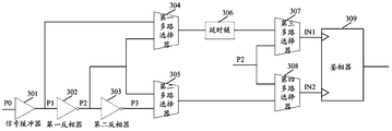
- the above-mentioned duty detection circuit 1053 includes a signal buffer 301, two inverters (including a first inverter 302 and a second inverter 303), and four multiplexers (including a first A multiplexer 304, a second multiplexer 305, a third multiplexer 307, and a fourth multiplexer 308) a delay chain 306 and a phase detector 309.
- the signal buffer 301 is coupled to the first inverter 302 and the first multiplexer 304.
- the first inverter 302 is coupled to the second inverter 303 and the first multiplexer. 304 and the second multiplexer 305, and the second inverter 303 is coupled to the second multiplexer 305.
- the first multiplexer 304 is coupled to the delay chain 306, the delay chain 306 is coupled to the third multiplexer 307, and the second multiplexer 305 is coupled to the fourth multiplexer 308.
- the first inverter 302 is also coupled to the third multiplexer 307 and the fourth multiplexer 308.
- the third multiplexer 307 and the fourth multiplexer 308 are respectively coupled to the phase detector 309.
- the reference clock signal input by the duty cycle detection circuit 1053 (that is, the above-mentioned signal buffer 301) is P0.
- the reference clock signal P0 passes through the signal buffer 301 to obtain a clock signal P1.
- the space ratio is the same as the reference clock signal P0 described above.
- the clock signal P1 passes through the first inverter 302 to obtain a clock signal P2.
- the frequency and amplitude of the clock signal P2 are the same as the clock signal P1, but the phase of the clock signal P2 is opposite to that of the clock signal P1.
- the duty cycle is equal to 1 minus the duty cycle of the clock signal P2; the clock signal P2 passes through the second inverter 303 to obtain a clock signal P3, and the frequency, amplitude and duty cycle of the clock signal P3 are the same as the above-mentioned clock signal P1 However, the phase of the clock signal P3 is opposite to that of the clock signal P2, that is, the phase of the clock signal P3 is the same as that of the clock signal P1.
- Mode 1 is to determine the duty cycle of the input signal by detecting the time T2 when the input signal is high; mode 2 is the time T1 to detect the input signal is low; mode 0 is to calibrate the phase detector 309.
- the first multiplexer 304 selects its first input signal (ie, the clock signal P1) and the second multiplexer. 305 strobes its second input signal (ie, clock signal P2. Clock signal P1 passes through the delay chain 306 to obtain a delayed clock signal P1.
- the third multiplexer 307 selects its first input signal (ie The delayed clock signal P1), that is, the first input signal (IN1) of the phase detector 309 is the delayed clock signal P1, and the fourth multiplexer 308 selects its second input signal (from The signal output from the second multiplexer 305), that is, the second input signal (IN2) of the phase detector 309 is a signal output from the second multiplexer 305.
- the timing diagrams of the above clock signals P0, P1, P2, and P3 are shown in FIG. 4A.
- the delay between the clock signal P2 and the clock signal P1 is INV1_D, that is, the clock signal is generated by the first inverter 302.
- the time delay is INV1_D
- the time delay between the clock signal P3 and the clock signal P2 is INV2_D, that is, the time delay caused by the clock signal passing through the second inverter 303 is INV2_D
- the duration of the flat signal is T1 and the duration of the high signal is T2. Since the clock signal P2 is obtained by the clock signal P1 through the inverter, the low signal duration of the clock signal P2 is T2 and the high signal duration is T1.
- the timing of the first input signal (IN1) and the second input signal (IN2) of the phase detector 309 is shown in FIG. 4B.
- the delays generated by the clock signal P1 after passing through the first multiplexer 304, the delay chain 306, and the third multiplexer 307 are MUX1_D, DLY_D, and MUX3_D, respectively.
- the clock signal P2 passes through the second multiplexer 305 and The delays generated after the fourth multiplexer 308 are MUX2_D and MUX4_D, respectively.
- the delay chain 306 generates a delay DLY_D for the clock signal P2.
- the first multiplexer 304 selects its second input signal (ie, the clock signal P2) and the second multiplexer. 305 strobes its second input signal (ie, the clock signal P2).
- the clock signal P2 passes through the delay chain 306 to obtain a delayed clock signal P2.
- the third multiplexer 307 selects its first input signal (that is, the delayed clock signal P2), that is, the first input signal (IN1) of the phase detector 309 is the delayed clock signal P2,
- the fourth multiplexer 308 selects its second input signal (that is, the signal output from the second multiplexer 305), that is, the second input signal (IN2) of the phase detector 309 is the second input signal (IN2) from the second multiplier. Signal output from the channel selector 305.
- the timing of the first input signal (IN1) and the second input signal (IN2) of the phase detector 309 is shown in FIG. 4C.
- the delays generated by the clock signal P2 after passing through the first multiplexer 304, the delay chain 306, and the third multiplexer 307 are MUX1_D, DLY_D, and MUX3_D, respectively.
- the clock signal P3 passes through the second multiplexer 305 and
- the delays generated after the fourth multiplexer 308 are MUX2_D and MUX4_D, respectively.
- the delay chain 306 generates a delay DLY_D for the clock signal P2.
- the delay time of the delay chain represents the relative relationship between T1 and T2.
- phase detector 309 obtains the delay duration DLY_D of the delay chain 309.
- the phase detector 309 presets three bit groups, including a coarse bit group, a medium bit group, and a fine bit group.
- the coarse adjustment bit group includes s1 bits
- the intermediate adjustment bit group includes s2 bits
- the fine adjustment bit group includes s3 bits.
- the phase detector 309 determines whether to perform coarse adjustment and intermediate adjustment.
- the phase detector 309 performs the coarse adjustment, as follows:
- the phase detector 309 waits for a first preset duration. The phase detector 309 then determines whether the rising edge of the first input signal (IN1) and the rising edge of the second input signal (IN2) are aligned, that is, whether the first input signal (IN1) and the second input signal (IN2) are aligned. There is a delay difference; when there is no delay difference between the first input signal (IN1) and the second input signal (IN2), the phase detector 309 sets the first bit position of the coarse adjustment bit group to 0; When there is a time delay difference between the input signal (IN1) and the second input signal (IN2), the phase detector 309 sets the first bit position of the coarse adjustment bit group to 1.
- the phase detector 309 repeatedly executes the above-mentioned process s1, and after performing the above-mentioned process s1, the s1 bits of the coarse adjustment bit group are all set to 0 or 1, and s1 is an integer greater than 1.
- the coarse adjustment bit group can be regarded as a character string composed of 0 and 1.
- phase detector 309 performs the middle adjustment, and the middle adjustment process is similar to the coarse adjustment process described above. details as follows:
- the phase detector 309 waits for a second preset duration. The phase detector 309 then determines whether there is a delay difference between the first input signal (IN1) and the second input signal (IN2); when there is no delay difference between the first input signal (IN1) and the second input signal (IN2) When the phase detector 309 sets the first bit position of the middle bit group to 0, when there is a delay difference between the first input signal (IN1) and the second input signal (IN2), the phase detector 309 sets the above The first bit position of the middle bit group is set.
- the phase detector 309 repeatedly executes the above-mentioned process s2 times, and after performing the above-mentioned process s2 times, the s2 bits of the coarse adjustment bit group are all set to 0 or 1, and s1 is an integer greater than 1.
- the middle bit group can be regarded as a character string composed of 0 and 1.
- the phase detector 309 When it is determined to skip the coarse adjustment and the middle adjustment, the phase detector 309 directly enters the fine adjustment.
- the fine adjustment process is similar to the coarse and middle adjustment process described above, and will not be described here.
- the fine-tuning bit group can be regarded as a string composed of 0 and 1.
- the phase detector 309 determines the delay time of the delay chain according to the coarse adjustment bit group, the medium adjustment bit group, and the fine adjustment bit group. Specifically, the phase detector 309 obtains the number of bits set to 1 in the coarse tuning bit group, the medium tuning bit group, and the fine tuning bit group, respectively.
- the number of bits set to 1 in the coarse bit group, the medium bit group, and the fine bit group is n1, n2, and n3, respectively.
- the delay time represented by each bit set to 1 in the coarse tuning bit group is t1 seconds
- the delay time represented by each bit set in the medium tuning bit group is 1 t2 seconds.
- the delay time represented by each bit set to 1 in the coarse tuning bit group is 0.5 nanosecond
- the delay time represented by each bit set in the above medium tuning bit group is 15 picoseconds.
- the delay time of each bit set to 1 in the fine adjustment bit group is 500 femtoseconds
- the phase detector 309 can obtain the delay time DLY_D of the delay chain.
- the above-mentioned duty cycle detection circuit further includes a microprocessor, which is configured to adjust the generation of the clock signal output by the first multiplexer 304 when the working mode is the mode 1 and the mode 2 So that the delay difference between the first input signal and the second input signal of the phase detector 309 is 0.
- the microprocessor obtains whether the phases of the two input signals (ie, IN1 and IN2) detected by the phase detector are 0.
- the microprocessor increases the delay
- the time delay of the first input signal of the third multiplexer 307 by the time chain increases the delay of the first input signal (ie, IN1) of the phase detector 309, so that the two inputs of the phase detector 309
- the phase difference of the signal decreases; when the phase detector 309 determines that the phase difference between its two input signals is not 0 and the first input signal (IN1) lags behind the second input signal (IN2), the microprocessor decreases The delay of the first input signal of the third demultiplexer 307 by the delay chain, thereby reducing the delay of the first input signal (ie, IN1) of the phase detector 309, making the two of the phase detector 309 two The phase
- the third multiplexer 307 selects its second input signal and the fourth multiplexer 308 selects its first An input signal, that is, the first input signal and the second input signal of the phase detector 309 are both P2. Because the delays of P2 by the third multiplexer 307 and the fourth multiplexer 308 are the same, the phase difference between the two signals input to the phase detector 309 is zero. In other words, the third multiplexer 307 and the fourth multiplexer 308 gate the same input signal into the phase detector 309. As shown in FIG. 4D, the phase difference between the first input signal (ie, IN1) and the second input signal (ie, IN2) of the phase detector 309 is 0.
Landscapes
- Physics & Mathematics (AREA)
- Nonlinear Science (AREA)
- Manipulation Of Pulses (AREA)
- Pulse Circuits (AREA)
Abstract
La présente invention concerne un circuit d'étalonnage de facteur de marche d'horloge de référence, comprenant un régulateur à faible chute de tension à faible bruit, un circuit d'oscillation, un circuit de réglage de facteur de marche et un circuit d'étalonnage de facteur de marche. Le circuit de détection de facteur de marche du circuit d'étalonnage de facteur de marche d'horloge de référence détecte le facteur de marche d'un signal d'horloge de référence délivré par le circuit de réglage de facteur de marche, et lorsqu'il est déterminé que le facteur de marche du signal d'horloge de référence s'écarte d'un facteur de marche prédéfini, le circuit de détection de facteur de marche ajuste l'amplitude du signal de sortie de celui-ci, et le facteur de marche du signal d'horloge de référence délivré par le circuit de réglage de facteur de marche est ajusté au moyen de la tension de sortie du circuit de conversion numérique-analogique et de la tension de sortie du régulateur différentiel basse tension à faible bruit. Le circuit d'étalonnage de facteur de marche d'horloge de référence de la présente invention peut être utilisé pour réduire efficacement le bruit de l'horloge de référence, améliorant les performances de communication.
Priority Applications (3)
| Application Number | Priority Date | Filing Date | Title |
|---|---|---|---|
| PCT/CN2018/091691 WO2019237366A1 (fr) | 2018-06-15 | 2018-06-15 | Circuit d'étalonnage de facteur de marche d'horloge de référence |
| EP18922591.5A EP3809594B1 (fr) | 2018-06-15 | 2018-06-15 | Circuit d'étalonnage de facteur de marche d'horloge de référence |
| CN201880094456.5A CN112262530B (zh) | 2018-06-15 | 2018-06-15 | 参考时钟占空比校准电路 |
Applications Claiming Priority (1)
| Application Number | Priority Date | Filing Date | Title |
|---|---|---|---|
| PCT/CN2018/091691 WO2019237366A1 (fr) | 2018-06-15 | 2018-06-15 | Circuit d'étalonnage de facteur de marche d'horloge de référence |
Publications (1)
| Publication Number | Publication Date |
|---|---|
| WO2019237366A1 true WO2019237366A1 (fr) | 2019-12-19 |
Family
ID=68841770
Family Applications (1)
| Application Number | Title | Priority Date | Filing Date |
|---|---|---|---|
| PCT/CN2018/091691 Ceased WO2019237366A1 (fr) | 2018-06-15 | 2018-06-15 | Circuit d'étalonnage de facteur de marche d'horloge de référence |
Country Status (3)
| Country | Link |
|---|---|
| EP (1) | EP3809594B1 (fr) |
| CN (1) | CN112262530B (fr) |
| WO (1) | WO2019237366A1 (fr) |
Cited By (1)
| Publication number | Priority date | Publication date | Assignee | Title |
|---|---|---|---|---|
| CN119727708A (zh) * | 2024-12-16 | 2025-03-28 | 慷智集成电路(上海)有限公司 | 一种锁相环参考时钟占空比校准电路 |
Families Citing this family (3)
| Publication number | Priority date | Publication date | Assignee | Title |
|---|---|---|---|---|
| CN113014233B (zh) * | 2021-03-10 | 2024-01-26 | 苏州芯捷联电子有限公司 | 时钟占空比校准电路 |
| CN117040494B (zh) * | 2023-10-08 | 2024-01-30 | 浙江大学 | 一种参考时钟校准电路、校准方法及参考时钟倍频器 |
| CN119727667B (zh) * | 2024-12-10 | 2025-08-08 | 合肥灿芯科技有限公司 | 一种占空比校准电路及方法 |
Citations (4)
| Publication number | Priority date | Publication date | Assignee | Title |
|---|---|---|---|---|
| US8471644B2 (en) * | 2011-01-19 | 2013-06-25 | Avago Technologies General Ip (Singapore) Pte. Ltd. | Digital automatic gain control circuits and methods for controlling the amplitude of a time-varying signal |
| US20140125390A1 (en) * | 2012-11-06 | 2014-05-08 | Micron Technology, Inc. | Apparatuses and methods for duty cycle adjustment |
| CN106656122A (zh) * | 2015-11-03 | 2017-05-10 | 三星电子株式会社 | 用于调节时钟信号中的占空比的装置和方法 |
| CN106961261A (zh) * | 2017-03-30 | 2017-07-18 | 中国电子科技集团公司第二十四研究所 | 一种低相噪可调占空比时钟信号源 |
Family Cites Families (6)
| Publication number | Priority date | Publication date | Assignee | Title |
|---|---|---|---|---|
| CN101227184B (zh) * | 2008-02-19 | 2011-06-22 | 东南大学 | 高速占空比校准电路 |
| JP5229081B2 (ja) * | 2009-04-10 | 2013-07-03 | 富士通株式会社 | 半導体装置 |
| US8513997B2 (en) * | 2010-09-30 | 2013-08-20 | St-Ericsson Sa | RF duty cycle correction circuit |
| US20130063191A1 (en) * | 2011-09-14 | 2013-03-14 | Rambus Inc. | Methods and Circuits for Duty-Cycle Correction |
| CN104753499B (zh) * | 2015-04-17 | 2017-05-24 | 上海华虹宏力半导体制造有限公司 | 占空比校准电路 |
| US9882570B1 (en) * | 2016-12-23 | 2018-01-30 | Inphi Corporation | Compact high speed duty cycle corrector |
-
2018
- 2018-06-15 CN CN201880094456.5A patent/CN112262530B/zh active Active
- 2018-06-15 EP EP18922591.5A patent/EP3809594B1/fr active Active
- 2018-06-15 WO PCT/CN2018/091691 patent/WO2019237366A1/fr not_active Ceased
Patent Citations (4)
| Publication number | Priority date | Publication date | Assignee | Title |
|---|---|---|---|---|
| US8471644B2 (en) * | 2011-01-19 | 2013-06-25 | Avago Technologies General Ip (Singapore) Pte. Ltd. | Digital automatic gain control circuits and methods for controlling the amplitude of a time-varying signal |
| US20140125390A1 (en) * | 2012-11-06 | 2014-05-08 | Micron Technology, Inc. | Apparatuses and methods for duty cycle adjustment |
| CN106656122A (zh) * | 2015-11-03 | 2017-05-10 | 三星电子株式会社 | 用于调节时钟信号中的占空比的装置和方法 |
| CN106961261A (zh) * | 2017-03-30 | 2017-07-18 | 中国电子科技集团公司第二十四研究所 | 一种低相噪可调占空比时钟信号源 |
Non-Patent Citations (1)
| Title |
|---|
| See also references of EP3809594A4 * |
Cited By (1)
| Publication number | Priority date | Publication date | Assignee | Title |
|---|---|---|---|---|
| CN119727708A (zh) * | 2024-12-16 | 2025-03-28 | 慷智集成电路(上海)有限公司 | 一种锁相环参考时钟占空比校准电路 |
Also Published As
| Publication number | Publication date |
|---|---|
| EP3809594B1 (fr) | 2022-10-26 |
| EP3809594A1 (fr) | 2021-04-21 |
| CN112262530B (zh) | 2023-07-11 |
| EP3809594A4 (fr) | 2021-07-14 |
| CN112262530A (zh) | 2021-01-22 |
Similar Documents
| Publication | Publication Date | Title |
|---|---|---|
| US6665351B2 (en) | Circuit and method for providing a digital data signal with pre-distortion | |
| US9209912B2 (en) | Circuit devices and methods for re-clocking an input signal | |
| WO2019237366A1 (fr) | Circuit d'étalonnage de facteur de marche d'horloge de référence | |
| KR102094684B1 (ko) | 다위상 클록 신호 보정 장치 | |
| US8384457B2 (en) | Duty cycle correction | |
| JP6250873B1 (ja) | デジタル/位相コンバータ | |
| US20100007393A1 (en) | Method and Apparatus for Achieving 50% Duty Cycle on the Output VCO of a Phased Locked Loop | |
| CN100454755C (zh) | 环形电压控制振荡器以及延迟单元电路 | |
| Nakamura et al. | A CMOS 50% duty cycle repeater using complementary phase blending | |
| US10419204B2 (en) | Serializer-deserializer with frequency doubler | |
| US8301093B2 (en) | Receiver circuit and data transmission system | |
| US20230121503A1 (en) | Calibration method, calibration device and multi-phase clock circuit | |
| US8508304B2 (en) | Serdes VCO with phased outputs driving frequency to voltage converter | |
| US9059837B1 (en) | Clock data recovery circuit and clock data recovery method | |
| KR101103070B1 (ko) | 클럭 신호 듀티 보정 회로 | |
| US10673443B1 (en) | Multi-ring cross-coupled voltage-controlled oscillator | |
| US9716505B2 (en) | System and method for enhanced clocking operation | |
| CN105830342B (zh) | 开关模式功率放大器的谐波抑制电路 | |
| KR20110014643A (ko) | 공급 전원 변동에 의한 지터 제거 방법 및 이를 적용한 디지털 제어 발진 회로 | |
| US7804347B2 (en) | Pulse generator circuit and communication apparatus | |
| KR100431999B1 (ko) | 자가 조절형 전압 제어 발진기 | |
| US7750744B2 (en) | Single-ended to differential translator to control current starved delay cell bias | |
| CN109217849B (zh) | 一种相位插值器 | |
| Kong et al. | A 21.5 mW 10+ Gb/s mm-Wave phased-array transmitter in 65nm CMOS | |
| JP2001094541A (ja) | クロックリカバリ回路 |
Legal Events
| Date | Code | Title | Description |
|---|---|---|---|
| 121 | Ep: the epo has been informed by wipo that ep was designated in this application |
Ref document number: 18922591 Country of ref document: EP Kind code of ref document: A1 |
|
| NENP | Non-entry into the national phase |
Ref country code: DE |
|
| ENP | Entry into the national phase |
Ref document number: 2018922591 Country of ref document: EP Effective date: 20210115 |