WO2019240136A1 - Afficheur à cristaux liquides - Google Patents
Afficheur à cristaux liquides Download PDFInfo
- Publication number
- WO2019240136A1 WO2019240136A1 PCT/JP2019/023133 JP2019023133W WO2019240136A1 WO 2019240136 A1 WO2019240136 A1 WO 2019240136A1 JP 2019023133 W JP2019023133 W JP 2019023133W WO 2019240136 A1 WO2019240136 A1 WO 2019240136A1
- Authority
- WO
- WIPO (PCT)
- Prior art keywords
- liquid crystal
- sealing material
- display device
- crystal display
- crystal layer
- Prior art date
- Legal status (The legal status is an assumption and is not a legal conclusion. Google has not performed a legal analysis and makes no representation as to the accuracy of the status listed.)
- Ceased
Links
Images


Classifications
-
- G—PHYSICS
- G02—OPTICS
- G02F—OPTICAL DEVICES OR ARRANGEMENTS FOR THE CONTROL OF LIGHT BY MODIFICATION OF THE OPTICAL PROPERTIES OF THE MEDIA OF THE ELEMENTS INVOLVED THEREIN; NON-LINEAR OPTICS; FREQUENCY-CHANGING OF LIGHT; OPTICAL LOGIC ELEMENTS; OPTICAL ANALOGUE/DIGITAL CONVERTERS
- G02F1/00—Devices or arrangements for the control of the intensity, colour, phase, polarisation or direction of light arriving from an independent light source, e.g. switching, gating or modulating; Non-linear optics
- G02F1/01—Devices or arrangements for the control of the intensity, colour, phase, polarisation or direction of light arriving from an independent light source, e.g. switching, gating or modulating; Non-linear optics for the control of the intensity, phase, polarisation or colour
- G02F1/13—Devices or arrangements for the control of the intensity, colour, phase, polarisation or direction of light arriving from an independent light source, e.g. switching, gating or modulating; Non-linear optics for the control of the intensity, phase, polarisation or colour based on liquid crystals, e.g. single liquid crystal display cells
- G02F1/133—Constructional arrangements; Operation of liquid crystal cells; Circuit arrangements
- G02F1/1333—Constructional arrangements; Manufacturing methods
- G02F1/1339—Gaskets; Spacers; Sealing of cells
-
- G—PHYSICS
- G09—EDUCATION; CRYPTOGRAPHY; DISPLAY; ADVERTISING; SEALS
- G09F—DISPLAYING; ADVERTISING; SIGNS; LABELS OR NAME-PLATES; SEALS
- G09F9/00—Indicating arrangements for variable information in which the information is built-up on a support by selection or combination of individual elements
- G09F9/30—Indicating arrangements for variable information in which the information is built-up on a support by selection or combination of individual elements in which the desired character or characters are formed by combining individual elements
Definitions
- the present invention relates to a liquid crystal display device.
- Liquid crystal display devices are used not only for normal life specifications such as watches and calculators, but also for in-vehicle applications that require high reliability. Since the in-vehicle liquid crystal display device has severe conditions of use environment, it is necessary to perform a reliability test before product shipment under severe conditions. Reliability testing includes environmental testing.
- a typical liquid crystal display device when an environmental test is performed in a high temperature and high humidity environment for a long time, moisture permeates the sealing material of the liquid crystal display device and moisture enters the liquid crystal layer. As a result of the specific resistance of the liquid crystal layer being lowered due to the moisture, a region where the retention rate of the capacitance is lowered is generated. As a result, a display defect occurs in the liquid crystal display device.
- the present invention provides a more reliable liquid crystal display device.
- a liquid crystal display device includes first and second substrates, a first liquid crystal layer sandwiched between the first and second substrates, and the first liquid crystal layer.
- a first sealing material that seals the first liquid crystal layer between the second substrates; and a second sealing material that surrounds the first sealing material with a space therebetween.
- a more reliable liquid crystal display device can be provided.
- FIG. 1 is a plan view of the liquid crystal display device according to the first embodiment.
- FIG. 2 is a cross-sectional view of the liquid crystal display device taken along line AA ′ of FIG.
- FIG. 3 is a diagram illustrating a specific cross-sectional structure of the liquid crystal display device.
- FIG. 4 is a plan view of a liquid crystal display device according to a comparative example.
- FIG. 5 is a plan view of the liquid crystal display device according to the second embodiment.
- FIG. 6 is a plan view of the liquid crystal display device according to the third embodiment.
- FIG. 7 is a plan view of the liquid crystal display device according to the fourth embodiment.
- FIG. 8 is a cross-sectional view of the liquid crystal display device taken along line BB ′ of FIG. FIG.
- FIG. 9 is a plan view of the liquid crystal display device according to the fifth embodiment.
- FIG. 10 is a cross-sectional view of the liquid crystal display device taken along line AA ′ of FIG.
- FIG. 11 is a plan view of a liquid crystal display device according to the sixth embodiment.
- FIG. 12 is a cross-sectional view of the liquid crystal display device taken along line AA ′ of FIG.
- FIG. 13 is a plan view of the liquid crystal display device according to the seventh embodiment.
- FIG. 14 is a cross-sectional view of the liquid crystal display device taken along line AA ′ of FIG.
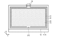
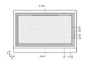
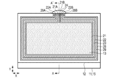
- FIG. 1 is a plan view of a liquid crystal display device 10 according to the first embodiment.
- FIG. 2 is a cross-sectional view of the liquid crystal display device 10 taken along line AA ′ of FIG.
- the sealing material and the sealing material are indicated by solid lines and the liquid crystal layer is indicated by dot hatching so that the configuration can be easily understood.
- the liquid crystal display device 10 includes a TFT substrate 11 on which TFTs, pixel electrodes, and the like are formed, and a color filter substrate (CF substrate) 12 on which color filters, common electrodes, and the like are formed and disposed opposite to the TFT substrate 11.
- a TFT substrate 11 on which TFTs, pixel electrodes, and the like are formed
- a color filter substrate (CF substrate) 12 on which color filters, common electrodes, and the like are formed and disposed opposite to the TFT substrate 11.
- Each of the TFT substrate 11 and the CF substrate 12 is composed of a transparent substrate (for example, a glass substrate or a plastic substrate).
- the liquid crystal layer 13 is filled between the TFT substrate 11 and the CF substrate 12. Specifically, the liquid crystal layer 13 is sealed in a region surrounded by the TFT substrate 11 and the CF substrate 12 and the sealing materials 21 and 22. The specific configuration of the sealing materials 21 and 22 will be described later.
- the liquid crystal material constituting the liquid crystal layer 13 changes its optical characteristics by manipulating the orientation of liquid crystal molecules according to the electric field applied between the TFT substrate 11 and the CF substrate 12.
- Various liquid crystal modes such as a VA (Vertical Alignment) mode, a TN (Twisted Nematic) mode, and a homogeneous mode can be applied as the liquid crystal mode.
- a plurality of switching elements (not shown) corresponding to a plurality of pixels are provided on the liquid crystal layer 13 side of the TFT substrate 11.
- the plurality of pixels are arranged in a matrix. The configuration of the switching element will be described later.
- An insulating layer 15 is provided on the plurality of switching elements.
- a plurality of pixel electrodes 16 corresponding to the plurality of pixels are provided on the insulating layer 15.
- One pixel electrode 16 is provided over substantially the entire pixel area.
- a color filter (not shown) is provided on the liquid crystal layer 13 side of the CF substrate 12.
- the configuration of the color filter will be described later.
- the common electrode 20 is provided on the color filter.
- the common electrode 20 is formed in a planar shape over the entire display area of the liquid crystal display device 10.
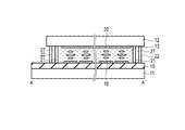
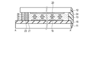
- FIG. 3 is a diagram for explaining a specific cross-sectional structure of the liquid crystal display device 10.
- FIG. 3 is a sectional view in which a part of the display area inside the sealing materials 21 and 22 is extracted, and is a sectional view along the X direction.
- a plurality of switching elements 14 corresponding to the plurality of pixels are provided on the liquid crystal layer 13 side of the TFT substrate 11.
- a TFT Thin-Film-Transistor
- an n-channel TFT is used.
- FIG. 3 shows the TFT 14 in a simplified manner.
- the TFT 14 includes a gate electrode functioning as a scanning line, a gate insulating film provided on the gate electrode, a semiconductor layer (for example, an amorphous silicon layer) provided on the gate insulating film, and a semiconductor layer.
- a source electrode and a drain electrode provided in contact with each other and spaced apart from each other; The source electrode is electrically connected to a signal line (not shown).
- a contact plug (contact hole) 17 electrically connected to the pixel electrode 16 is provided in the insulating layer 15 and on the drain electrode of the TFT 14.
- An alignment film (not shown) for controlling the initial alignment of the liquid crystal layer 13 is provided on the insulating layer 15 and the plurality of pixel electrodes 16.
- a color filter 18 is provided on the liquid crystal layer 13 side of the CF substrate 12.
- the color filter 18 includes a plurality of coloring filters (coloring members), and specifically includes a plurality of red filters 18-R, a plurality of green filters 18-G, and a plurality of blue filters 18-B.
- a general color filter is composed of three primary colors of light, red (R), green (G), and blue (B).
- a set of three colors R, G, and B adjacent to each other is a display unit (pixel), and any single color portion of R, G, B in one pixel is a minimum called a subpixel (subpixel). It is a drive unit.
- the TFT 14 and the pixel electrode 16 are provided for each subpixel.
- the sub-pixel is referred to as a pixel unless it is particularly necessary to distinguish between the pixel and the sub-pixel.
- a black matrix (light shielding layer) 19 for light shielding is provided at the boundary portion of the red filter 18-R, the green filter 18-G, and the blue filter 18-B, and the boundary portion of the pixel (sub pixel). That is, the black matrix 19 is formed in a mesh shape.
- the black matrix 19 has a function of shielding unnecessary light between the coloring members and improving the contrast.
- An alignment film (not shown) for controlling the initial alignment of the liquid crystal layer 13 is provided on the common electrode 20.
- the pixel electrode 16, the contact plug 17, and the common electrode 20 are made of transparent electrodes, and for example, ITO (indium tin oxide) is used.
- ITO indium tin oxide
- a transparent insulating material is used, for example, silicon nitride (SiN).
- the sealing material 21 is provided in contact with the insulating layer 15 and the CF substrate 12.
- the sealing material 21 has a frame shape and a quadrangle, for example. That is, the sealing material 21 includes two sides extending in the X direction and two sides extending in the Y direction orthogonal to the X direction.
- the area inside the sealing material 21 is a display area where an image can be displayed.
- the sealing material 22 is provided in contact with the insulating layer 15 and the CF substrate 12.
- the sealing material 22 has, for example, a frame shape and a quadrangular shape.
- the sealing material 22 is configured to surround the sealing material 21.
- the sealing material 22 is disposed outside the sealing material 21 with a space from the sealing material 21.
- a liquid crystal layer 23 is provided between the sealing material 21 and the sealing material 22.
- the liquid crystal layer 23 is made of the same material as the liquid crystal layer 13, for example.
- the sealing material 21 has, for example, an injection port (opening) for injecting liquid crystal at the center of the upper side (side extending in the X direction) in FIG.
- the inlet of the sealing material 21 is composed of two sealing materials 21A and 21B extending in the Y direction from a part of the rectangular sealing material.
- the sealing materials 21 ⁇ / b> A and 21 ⁇ / b> B extend to the end of the TFT substrate 11.
- the sealing material 22 has, for example, an injection port for injecting liquid crystal at the center of the upper side (side extending in the X direction) in FIG.
- the inlet of the sealing material 22 is composed of two sealing materials 22A and 22B extending in the Y direction from a part of the rectangular sealing material.
- the sealing materials 22A and 22B extend to the end of the TFT substrate 11.
- the sealing materials 21 and 22 are formed by printing, for example.
- the sealing material is made of, for example, an ultraviolet curable resin, a thermosetting resin, or an ultraviolet / heat combination type curable resin, and is printed on the TFT substrate 11 and / or the CF substrate 12 in the manufacturing process, and then irradiated with ultraviolet rays or heated. Can be cured.
- the sealing material 24 seals the inlet of the sealing material 21 and the inlet of the sealing material 22.
- the sealing material 24 is made of, for example, an ultraviolet curable resin. After the liquid crystal is injected between the TFT substrate 11 and the CF substrate 12, the sealing material 24 is applied so as to fill the injection port of the sealing material 21 and the injection port of the sealing material 22. Thereafter, the sealing material 24 is cured by ultraviolet irradiation.
- liquid crystal injection method for example, a vacuum injection method can be used.
- liquid crystal is injected from the inlets of the sealing materials 21 and 22.
- liquid crystal display device 10 configured as described above, moisture can be prevented from entering the liquid crystal layer 13 from the outside.
- the outer sealing material 22 may be made of a material having a higher barrier property.
- the sealing material 22 is composed of a sealing material containing an inorganic material.
- As the inorganic material a material that does not transmit moisture is selected.
- the inner sealing material 21 is made of resin, for example.
- the barrier property of the sealing material 22 can be further increased. Thereby, it can suppress more that the liquid crystal layer 13 permeates moisture.
- FIG. 4 is a plan view of a liquid crystal display device according to a comparative example.
- the liquid crystal layer 13 is sealed between the TFT substrate 11 and the CF substrate 12 by a single layer of sealing material 22.
- the inlet of the sealing material 22 is sealed with a sealing material 24.
- the liquid crystal display device may be mounted on, for example, a vehicle having a severe use environment. High reliability is required for an in-vehicle liquid crystal display device. For this reason, a reliability test (environmental test) is performed under more severe conditions.
- a test for maintaining a high-temperature and high-humidity environment for example, 85 degrees, 85% RH (relative humidity) for 2000 hours (hours) is performed.
- the capacitance of the display region (particularly, at the four corners of the sealant 22 near the sealant 22) is reduced.
- An area with a reduced retention rate is created. This is because moisture in a high-temperature and high-humidity environment penetrates the sealing material 22 and enters the liquid crystal layer 13, and the specific resistance of the liquid crystal is reduced due to the moisture, resulting in a decrease in capacitance retention. It is.
- the liquid crystal display device according to the comparative example cannot realize a normal display operation.
- the liquid crystal display device 10 has a structure in which moisture hardly enters the liquid crystal layer 13 from the outside.
- moisture that has passed through the sealing material 22 is absorbed by the liquid crystal layer 23, it is possible to suppress moisture from entering the liquid crystal layer 13 through the sealing material 21.
- the liquid crystal display device 10 includes the liquid crystal layer 13 sandwiched between the TFT substrate 11 and the CF substrate 12 and the liquid crystal layer 13.
- a sealing material 21 that encloses and seals the liquid crystal layer 13 between the TFT substrate 11 and the CF substrate 12, a sealing material 22 that surrounds the sealing material 21 with a space therebetween, and a liquid crystal layer 23 provided between the sealing materials 21 and 22.
- liquid crystal display device 10 when an environmental test is performed on the liquid crystal display device 10, moisture that has passed through the outer sealing material 22 is absorbed by the liquid crystal layer 23 and blocked by the sealing material 22. Thereby, it is possible to suppress moisture from entering the liquid crystal layer 13. According to 1st Embodiment, it can suppress that the liquid crystal display device 10 becomes defective, and the liquid crystal display device 10 with higher reliability is realizable.
- the liquid crystal display device 10 according to the present embodiment is particularly effective for applications that require high reliability such as in-vehicle use.
- the inlet of the sealing material 21 and the inlet of the sealing material 22 are arranged at the same position. Thereby, the injection
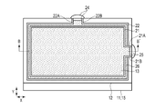
- FIG. 5 is a plan view of a liquid crystal display device 10 according to a second embodiment.
- the sealing material 21 has an opening 21C in the center of the lower side (side extending in the X direction) of FIG. Unlike the first embodiment, the sealing material 21 is not provided with an inlet in the center of the upper side (side extending in the X direction) in FIG.
- the sealing material 22 has an inlet at the center of the upper side (side extending in the X direction) in FIG.
- the liquid crystal is injected between the TFT substrate 11 and the CF substrate 12 from the injection port of the sealing material 22.
- the liquid crystal injected inside the sealing material 22 is further injected inside the sealing material 21 through the opening 21 ⁇ / b> C of the sealing material 21.
- the sealing material 24 seals the inlet of the sealing material 22.
- Much moisture may enter from the vicinity of the sealing material 24.
- the opening 21 ⁇ / b> C of the sealing material 21 is arranged at a position that is larger than the inlet of the sealing material 22, moisture that has entered the liquid crystal layer 23 from the vicinity of the sealing material 24 Invasion inside can be suppressed.
- FIG. 6 is a plan view of a liquid crystal display device 10 according to a third embodiment.
- the liquid crystal display device 10 does not include the sealing material 24 for sealing the liquid crystal shown in the first embodiment.
- the sealing material 21 has, for example, a frame shape and a square shape.
- the sealing material 21 does not have an injection port for injecting liquid crystal.
- the sealing material 22 has, for example, a frame shape and a quadrangular shape.
- the sealing material 22 does not have an injection port for injecting liquid crystal.
- a liquid crystal layer 23 is provided between the sealing material 21 and the sealing material 22.
- an ODF (one drop fill) method is used as a liquid crystal injection method.
- a liquid crystal injection port is unnecessary.
- the ODF method after a sealing material is printed on one or two substrates, a liquid crystal is filled in a region surrounded by the sealing material. Thereafter, the two substrates are bonded together.
- FIG. 7 is a plan view of a liquid crystal display device 10 according to a fourth embodiment.
- FIG. 8 is a cross-sectional view of the liquid crystal display device 10 taken along the line BB ′ of FIG.
- the sealing material 21 has, for example, an injection port for injecting liquid crystal at the center of the right side (side extending in the Y direction) in FIG.
- the inlet of the sealing material 21 is composed of two sealing materials 21A and 21B extending in the X direction from a part of the rectangular sealing material.
- the sealing materials 21 ⁇ / b> A and 21 ⁇ / b> B extend to the end of the TFT substrate 11.
- the sealing material 22 has, for example, an injection port for injecting a substance at the center of the upper side (side extending in the X direction) in FIG.
- the inlet of the sealing material 22 is composed of two sealing materials 22 ⁇ / b> A and 22 ⁇ / b> B extending in the Y direction from the central portion of the upper side of the sealing material 22.
- the sealing materials 22A and 22B extend to the end of the TFT substrate 11.
- the right side of the sealing material 22 is divided by the sealing materials 21A and 21B, and the divided portions of the sealing material 22 are in contact with the sealing materials 21A and 21B.
- a filling layer (absorbing material) 26 made of a substance different from the liquid crystal layer 13 and having water absorption is provided.
- the filling layer 26 has a function of absorbing moisture that has passed through the sealing material 22.
- Examples of the packed layer 26 include silica gel for solids and polyvinyl alcohol or polyethylene glycol for polymers.
- the liquid crystal layer 13 is injected from the inlet of the sealing material 21.
- the filling layer 26 is injected from the inlet of the sealing material 22.
- the sealing material 25 seals the inlet of the sealing material 21.
- the sealing material 24 seals the inlet of the sealing material 22.
- the sealing materials 24 and 25 are made of, for example, an ultraviolet curable resin.
- moisture that has passed through the sealing material 22 is absorbed by the filling layer 26. Thereby, it is possible to suppress moisture from entering the liquid crystal layer 13.
- FIG. 9 is a plan view of a liquid crystal display device 10 according to a fifth embodiment.
- FIG. 10 is a cross-sectional view of the liquid crystal display device 10 taken along line AA ′ of FIG.
- the shapes of the sealing materials 21 and 22 are the same as those in the third embodiment.
- An air layer 27 is provided between the sealing material 21 and the sealing material 22. That is, no substance is injected between the sealing material 21 and the sealing material 22.
- the outer sealing material 22 is made of a material having higher barrier properties, for example, a sealing material containing an inorganic material.
- the inner sealing material 21 is made of resin, for example.
- the ODF method is used as the liquid crystal injection method. Also in the fifth embodiment, moisture can be prevented from entering the liquid crystal layer 13.
- FIG. 11 is a plan view of a liquid crystal display device 10 according to a sixth embodiment.
- FIG. 12 is a cross-sectional view of the liquid crystal display device 10 taken along the line AA ′ of FIG.
- the liquid crystal display device 10 includes three layers of sealing materials 21, 22, and 28.
- the sealing material 28 is provided in contact with the insulating layer 15 and the CF substrate 12.
- the sealing material 28 has a frame shape and a quadrangle, for example.
- the sealing material 28 is configured to surround the sealing material 22.
- the sealing material 28 is disposed outside the sealing material 22 with a space from the sealing material 22.
- a liquid crystal layer 29 is provided between the sealing material 22 and the sealing material 28.
- the sealing material 28 has an injection port for injecting liquid crystal at the same position as the injection ports of the sealing materials 21 and 22. That is, the inlet of the sealing material 28 is constituted by two sealing materials 28A and 28B extending in the Y direction from the central portion of the upper side of the sealing material 28. The sealing materials 28A and 28B extend to the end of the TFT substrate 11.
- the liquid crystal display device 10 includes the three layers of sealing materials 21, 22, and 28, and the two layers of liquid crystal layers 23 and 29, so that moisture enters the liquid crystal layer 13. It can be suppressed more.
- FIG. 13 is a plan view of a liquid crystal display device 10 according to a seventh embodiment.
- FIG. 14 is a cross-sectional view of the liquid crystal display device 10 taken along line AA ′ of FIG.
- the liquid crystal display device 10 includes three layers of sealing materials 21, 22, and 28.
- An air layer 27 is provided between the sealing material 21 and the sealing material 22. That is, no substance is injected between the sealing material 21 and the sealing material 22. For example, the air layer 27 is sealed by the sealing material 21 and the sealing material 22.
- the sealing materials 21 and 28 have an injection port for injecting liquid crystal at the same position (for example, the central portion of the upper side in FIG. 1).
- the upper side of the sealing material 22 is divided by the sealing materials 21A and 21B, and the divided portions of the sealing material 22 are in contact with the sealing materials 21A and 21B.
- moisture can be prevented from entering the liquid crystal layer 13.
- the first to seventh embodiments can be combined as appropriate.
- a sealing material having an inorganic material may be applied to one or more of the plurality of sealing materials of the first to seventh embodiments.
- a filling layer having water absorption may be applied to the liquid crystal layers of the first to seventh embodiments.
- the type of liquid crystal display device is not limited, and can be applied to various types of liquid crystal display devices.
- the liquid crystal display device may be a simple matrix type.
- the sealing material is configured to contact two opposing substrates.
- the present invention is not limited to the embodiment described above, and can be embodied by modifying the constituent elements without departing from the scope of the invention. Further, the above embodiments include inventions at various stages, and are obtained by appropriately combining a plurality of constituent elements disclosed in one embodiment or by appropriately combining constituent elements disclosed in different embodiments. Various inventions can be configured. For example, even if some constituent elements are deleted from all the constituent elements disclosed in the embodiment, the problems to be solved by the invention can be solved and the effects of the invention can be obtained. Embodiments made can be extracted as inventions.
Landscapes
- Physics & Mathematics (AREA)
- Nonlinear Science (AREA)
- General Physics & Mathematics (AREA)
- Mathematical Physics (AREA)
- Chemical & Material Sciences (AREA)
- Crystallography & Structural Chemistry (AREA)
- Optics & Photonics (AREA)
- Engineering & Computer Science (AREA)
- Theoretical Computer Science (AREA)
- Liquid Crystal (AREA)
- Devices For Indicating Variable Information By Combining Individual Elements (AREA)
Abstract
La présente invention concerne un afficheur à cristaux liquides comprenant : des premier et deuxième substrats (11, 12) ; une couche de cristaux liquides (13) qui est maintenue entre les premier et deuxième substrats (11, 12) ; un premier matériau d'étanchéité (21) qui entoure la couche de cristaux liquides (13) et qui enferme hermétiquement la couche de cristaux liquides (13) entre les premier et deuxième substrats (11, 12) ; et un deuxième matériau d'étanchéité (22) qui entoure le premier matériau d'étanchéité (21) à une certaine distance de celui-ci.
Applications Claiming Priority (2)
| Application Number | Priority Date | Filing Date | Title |
|---|---|---|---|
| JP2018111696A JP2019215410A (ja) | 2018-06-12 | 2018-06-12 | 液晶表示装置 |
| JP2018-111696 | 2018-06-12 |
Publications (1)
| Publication Number | Publication Date |
|---|---|
| WO2019240136A1 true WO2019240136A1 (fr) | 2019-12-19 |
Family
ID=68842004
Family Applications (1)
| Application Number | Title | Priority Date | Filing Date |
|---|---|---|---|
| PCT/JP2019/023133 Ceased WO2019240136A1 (fr) | 2018-06-12 | 2019-06-11 | Afficheur à cristaux liquides |
Country Status (3)
| Country | Link |
|---|---|
| JP (1) | JP2019215410A (fr) |
| TW (1) | TWI703389B (fr) |
| WO (1) | WO2019240136A1 (fr) |
Cited By (2)
| Publication number | Priority date | Publication date | Assignee | Title |
|---|---|---|---|---|
| CN116685898A (zh) * | 2021-12-31 | 2023-09-01 | 京东方科技集团股份有限公司 | 一种调光玻璃及其制备方法和车辆 |
| EP4556992A1 (fr) * | 2023-11-15 | 2025-05-21 | LG Display Co., Ltd. | Dispositif d'affichage |
Citations (7)
| Publication number | Priority date | Publication date | Assignee | Title |
|---|---|---|---|---|
| JPS59156223U (ja) * | 1983-04-05 | 1984-10-20 | シチズン時計株式会社 | 液晶表示セルの構造 |
| JPH0335528U (fr) * | 1989-08-15 | 1991-04-08 | ||
| JP2002258291A (ja) * | 2001-02-28 | 2002-09-11 | Toshiba Corp | 液晶表示素子 |
| JP2002350882A (ja) * | 2001-05-30 | 2002-12-04 | Optrex Corp | 液晶表示パネル |
| WO2007007394A1 (fr) * | 2005-07-11 | 2007-01-18 | Fujitsu Limited | Élément d’affichage à cristaux liquides |
| JP2014010211A (ja) * | 2012-06-28 | 2014-01-20 | Seiko Epson Corp | 液晶装置、液晶装置の製造方法、電子機器 |
| JP2014145890A (ja) * | 2013-01-29 | 2014-08-14 | Seiko Epson Corp | 電気光学装置および電子機器 |
Family Cites Families (7)
| Publication number | Priority date | Publication date | Assignee | Title |
|---|---|---|---|---|
| JPH07281199A (ja) * | 1994-02-15 | 1995-10-27 | Sanyo Electric Co Ltd | 液晶表示装置 |
| US6650392B2 (en) * | 2000-03-15 | 2003-11-18 | Kabushiki Kaisha Toshiba | Cell structure of liquid crystal device |
| JP2001264777A (ja) * | 2000-03-15 | 2001-09-26 | Toshiba Corp | 液晶セル |
| JP2007240690A (ja) * | 2006-03-07 | 2007-09-20 | Seiko Epson Corp | 液晶装置及びその製造方法、並びに電子機器 |
| JP2013218234A (ja) * | 2012-04-12 | 2013-10-24 | Seiko Epson Corp | 電気光学装置、及び電子機器 |
| JP2013222019A (ja) * | 2012-04-16 | 2013-10-28 | Mitsubishi Electric Corp | 液晶パネルおよびこれを有する液晶表示装置 |
| US9625764B2 (en) * | 2012-08-28 | 2017-04-18 | Semiconductor Energy Laboratory Co., Ltd. | Display device and electronic device |
-
2018
- 2018-06-12 JP JP2018111696A patent/JP2019215410A/ja active Pending
-
2019
- 2019-06-11 TW TW108120047A patent/TWI703389B/zh not_active IP Right Cessation
- 2019-06-11 WO PCT/JP2019/023133 patent/WO2019240136A1/fr not_active Ceased
Patent Citations (7)
| Publication number | Priority date | Publication date | Assignee | Title |
|---|---|---|---|---|
| JPS59156223U (ja) * | 1983-04-05 | 1984-10-20 | シチズン時計株式会社 | 液晶表示セルの構造 |
| JPH0335528U (fr) * | 1989-08-15 | 1991-04-08 | ||
| JP2002258291A (ja) * | 2001-02-28 | 2002-09-11 | Toshiba Corp | 液晶表示素子 |
| JP2002350882A (ja) * | 2001-05-30 | 2002-12-04 | Optrex Corp | 液晶表示パネル |
| WO2007007394A1 (fr) * | 2005-07-11 | 2007-01-18 | Fujitsu Limited | Élément d’affichage à cristaux liquides |
| JP2014010211A (ja) * | 2012-06-28 | 2014-01-20 | Seiko Epson Corp | 液晶装置、液晶装置の製造方法、電子機器 |
| JP2014145890A (ja) * | 2013-01-29 | 2014-08-14 | Seiko Epson Corp | 電気光学装置および電子機器 |
Cited By (3)
| Publication number | Priority date | Publication date | Assignee | Title |
|---|---|---|---|---|
| CN116685898A (zh) * | 2021-12-31 | 2023-09-01 | 京东方科技集团股份有限公司 | 一种调光玻璃及其制备方法和车辆 |
| US20250044648A1 (en) * | 2021-12-31 | 2025-02-06 | Beijing Boe Sensor Technology Co., Ltd. | Light-adjusting glass, manufacturing method thereof and vehicle |
| EP4556992A1 (fr) * | 2023-11-15 | 2025-05-21 | LG Display Co., Ltd. | Dispositif d'affichage |
Also Published As
| Publication number | Publication date |
|---|---|
| JP2019215410A (ja) | 2019-12-19 |
| TWI703389B (zh) | 2020-09-01 |
| TW202004299A (zh) | 2020-01-16 |
Similar Documents
| Publication | Publication Date | Title |
|---|---|---|
| US11644718B2 (en) | Liquid crystal display device | |
| US10690974B2 (en) | Liquid crystal display device | |
| JP6542986B2 (ja) | Va型coa液晶表示パネル | |
| US9638968B2 (en) | Color liquid crystal display panel and manufacturing method thereof | |
| US9298052B2 (en) | Display apparatus | |
| EP2749934B1 (fr) | Panneau à cristaux liquides | |
| CN103941446A (zh) | 显示器件 | |
| WO2011145258A1 (fr) | Dispositif d'affichage, et procédé de fabrication de celui-ci | |
| TWI703389B (zh) | 液晶顯示裝置 | |
| KR20080050822A (ko) | 액정표시장치 | |
| CN106154619B (zh) | 显示面板 | |
| US8773630B2 (en) | Display device | |
| JP5042467B2 (ja) | 液晶表示装置および液晶パネル | |
| JP4004457B2 (ja) | 液晶パネルの周辺構造 | |
| JP2010175727A (ja) | 液晶表示装置 | |
| JP6498016B2 (ja) | 液晶パネルおよび液晶表示装置 | |
| JP2009223021A (ja) | 表示素子 | |
| JP2008015374A (ja) | 液晶表示装置 |
Legal Events
| Date | Code | Title | Description |
|---|---|---|---|
| 121 | Ep: the epo has been informed by wipo that ep was designated in this application |
Ref document number: 19819509 Country of ref document: EP Kind code of ref document: A1 |
|
| NENP | Non-entry into the national phase |
Ref country code: DE |
|
| 122 | Ep: pct application non-entry in european phase |
Ref document number: 19819509 Country of ref document: EP Kind code of ref document: A1 |