WO2019244502A1 - Convertisseur de courant électrique - Google Patents
Convertisseur de courant électrique Download PDFInfo
- Publication number
- WO2019244502A1 WO2019244502A1 PCT/JP2019/018691 JP2019018691W WO2019244502A1 WO 2019244502 A1 WO2019244502 A1 WO 2019244502A1 JP 2019018691 W JP2019018691 W JP 2019018691W WO 2019244502 A1 WO2019244502 A1 WO 2019244502A1
- Authority
- WO
- WIPO (PCT)
- Prior art keywords
- cooling
- bus bar
- cooler
- connector
- semiconductor module
- Prior art date
- Legal status (The legal status is an assumption and is not a legal conclusion. Google has not performed a legal analysis and makes no representation as to the accuracy of the status listed.)
- Ceased
Links
Images


Classifications
-
- H—ELECTRICITY
- H02—GENERATION; CONVERSION OR DISTRIBUTION OF ELECTRIC POWER
- H02M—APPARATUS FOR CONVERSION BETWEEN AC AND AC, BETWEEN AC AND DC, OR BETWEEN DC AND DC, AND FOR USE WITH MAINS OR SIMILAR POWER SUPPLY SYSTEMS; CONVERSION OF DC OR AC INPUT POWER INTO SURGE OUTPUT POWER; CONTROL OR REGULATION THEREOF
- H02M7/00—Conversion of AC power input into DC power output; Conversion of DC power input into AC power output
- H02M7/42—Conversion of DC power input into AC power output without possibility of reversal
- H02M7/44—Conversion of DC power input into AC power output without possibility of reversal by static converters
- H02M7/48—Conversion of DC power input into AC power output without possibility of reversal by static converters using discharge tubes with control electrode or semiconductor devices with control electrode
-
- H—ELECTRICITY
- H05—ELECTRIC TECHNIQUES NOT OTHERWISE PROVIDED FOR
- H05K—PRINTED CIRCUITS; CASINGS OR CONSTRUCTIONAL DETAILS OF ELECTRIC APPARATUS; MANUFACTURE OF ASSEMBLAGES OF ELECTRICAL COMPONENTS
- H05K7/00—Constructional details common to different types of electric apparatus
- H05K7/02—Arrangements of circuit components or wiring on supporting structure
- H05K7/06—Arrangements of circuit components or wiring on supporting structure on insulating boards, e.g. wiring harnesses
-
- H—ELECTRICITY
- H05—ELECTRIC TECHNIQUES NOT OTHERWISE PROVIDED FOR
- H05K—PRINTED CIRCUITS; CASINGS OR CONSTRUCTIONAL DETAILS OF ELECTRIC APPARATUS; MANUFACTURE OF ASSEMBLAGES OF ELECTRICAL COMPONENTS
- H05K7/00—Constructional details common to different types of electric apparatus
- H05K7/20—Modifications to facilitate cooling, ventilating, or heating
-
- H—ELECTRICITY
- H10—SEMICONDUCTOR DEVICES; ELECTRIC SOLID-STATE DEVICES NOT OTHERWISE PROVIDED FOR
- H10W—GENERIC PACKAGES, INTERCONNECTIONS, CONNECTORS OR OTHER CONSTRUCTIONAL DETAILS OF DEVICES COVERED BY CLASS H10
- H10W40/00—Arrangements for thermal protection or thermal control
-
- H—ELECTRICITY
- H10—SEMICONDUCTOR DEVICES; ELECTRIC SOLID-STATE DEVICES NOT OTHERWISE PROVIDED FOR
- H10W—GENERIC PACKAGES, INTERCONNECTIONS, CONNECTORS OR OTHER CONSTRUCTIONAL DETAILS OF DEVICES COVERED BY CLASS H10
- H10W90/00—Package configurations
Definitions
- the present disclosure relates to a power conversion device.
- ⁇ Power converters such as inverters have electronic components such as capacitors, current sensors, and reactors, in addition to semiconductor modules. These electronic components are arranged in a case.
- the case is provided with a high-voltage connector such as an input connector or an output connector for electrical connection to an external DC power supply, an AC load, or the like.
- Patent Document 2 discloses a power control unit as a power conversion device mounted on a vehicle such as an electric vehicle or a hybrid vehicle.
- This power control unit is a device for supplying AC power to a traveling motor, and includes a cooler for cooling an inverter circuit, and a bus bar for electrical connection with other connected devices. I have.
- the bus bar is arranged so as to be in contact with the outer surface of the outer wall portion corresponding to the cooler in the housing of the power control unit.
- the power control unit disclosed in Patent Document 2 has a configuration in which the cooler contacts the inner surface of the outer wall while the bus bar contacts the outer surface of the outer wall, and the bus bar is cooled by the cooler from the inside of the outer wall. It is configured. In the case of this configuration, by arranging the bus bar on the outside of the housing, the bus bar becomes longer and the resistance increases, so that heat generation increases. In addition, since the outer wall is interposed between the bus bar, which is a heating element, and the cooler, heat generated in the bus bar is less likely to move to the cooler through the outer wall. Therefore, it is difficult to obtain a high cooling effect for the connected devices connected to the bus bar.
- the present disclosure seeks to provide a power conversion device that can extend the life of electronic components.
- a first aspect of the present disclosure includes a semiconductor module, A cooler for cooling the semiconductor module, Electronic components directly or indirectly connected to the semiconductor module, A high-voltage connector connected to an external device; A connector connection bus bar for connecting between the high-voltage connector and the electronic component, At least one of the connector connection bus bars is a heat dissipation bus bar disposed adjacent to the cooler, a power conversion device, It is in.
- a second aspect of the present disclosure is directed to a semiconductor module provided in an energization path between a power supply and a motor, A cooler for cooling the semiconductor module, A connection device electrically connected to the semiconductor module via a bus bar, A cooling module for connecting the connection device to the cooler so as to be able to conduct heat, A power conversion device comprising: It is in.
- At least one of the connector connection bus bars that connects the high-voltage connector and the electronic component is a heat radiation bus bar that is arranged adjacent to the cooler. Therefore, even if the heat of the high-voltage connector is transmitted to the connector connection bus bar, at least a part of the heat can be radiated from the heat radiating bus bar to the cooler. Thus, heat transmitted to the electronic component via the connector connection bus bar can be suppressed. As a result, the life of the electronic component can be extended.
- the cooler has a function of cooling the semiconductor module provided in the power supply path between the power supply and the motor.
- the cooling module connects a connection device electrically connected to the semiconductor module via the bus bar to the cooler so as to be able to conduct heat.
- the connection device is indirectly cooled using the cooling module cooled by the cooler as the cooling source. That is, the heat of the connected device is transmitted from the cooling module to the cooler and is radiated. Therefore, even when the bus bar generates heat during energization, it is possible to prevent the connected devices electrically connected to the bus bar from becoming hot. In particular, when the heat resistance of the connected device is low, the influence of heat on the connected device can be reduced by using the cooling module.
- the cooling function of the cooler is used not only for cooling the semiconductor module but also for cooling the connected devices via the cooling module. That is, the cooler is also used for cooling for the connected device. For this reason, it is not necessary to provide a dedicated cooler for the connected device, and it is possible to prevent the entire device from becoming large and from being deteriorated in vehicle mountability. As a result, it is possible to extend the life of an electronic component such as a connected device.
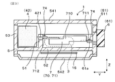
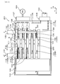
- FIG. 1 is an explanatory cross-sectional view of a power conversion device according to a first embodiment viewed from a Z direction.
- FIG. 2 is an explanatory sectional view taken along line II-II of FIG.
- FIG. 3 is an explanatory sectional view taken along line III-III in FIG.
- FIG. 4 is a cross-sectional explanatory view of the power converter according to the second embodiment as viewed from the Z direction.
- FIG. 5 is an explanatory cross-sectional view of the power converter according to the third embodiment as viewed from the Z direction.
- FIG. 6 is an explanatory cross-sectional view of the power converter according to the fourth embodiment as viewed from the Z direction.
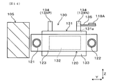
- FIG. 7 is a diagram illustrating an overall structure of a power conversion device according to a fifth embodiment;
- FIG. 8 is a sectional view taken along line VIII-VIII in FIG.
- FIG. 9 is a sectional view taken along line IX-IX in FIG.
- FIG. 10 is a sectional view taken along line XX of FIG.
- FIG. 11 is a sectional view taken along line XI-XI in FIG.
- FIG. 12 is an inverter circuit diagram of the power converter according to the fifth embodiment.
- FIG. 13 is a diagram illustrating an overall structure of a power conversion device according to a sixth embodiment;
- FIG. 14 is a sectional view taken along line XIV-XIV in FIG.
- the power conversion device 1 of the present embodiment includes a semiconductor module 2, a cooler 3, an electronic component 4, a high-voltage connector 6, and a connector connection bus bar 7.
- the cooler 3 cools the semiconductor module 2.
- the electronic component 4 is directly or indirectly connected to the semiconductor module 2.
- the high-voltage connector 6 is a connector connected to an external device.
- the connector connection bus bar 7 is a bus bar that connects between the high-voltage connector 6 and the electronic component 4. At least one of the connector connection bus bars 7 is a heat radiating bus bar 70 disposed adjacent to the cooler 3.
- the power conversion device 1 of the present embodiment has an input connector 61 and an output connector 62 as the high-voltage connector 6.
- the input connector 61 is configured to be connected to a connector of a power supply line connected to a DC power supply.
- the output connector 62 is configured to be connected to a connector of a load wiring connected to an AC load such as a rotating electric machine.
- the power conversion device 1 has a plurality of input bus bars 71 connected to the input connector 61 and a plurality of output bus bars 72 connected to the output connector 62 as the connector connection bus bar 7.
- the input bus bar 71 of the connector connection bus bar 7 is the heat radiating bus bar 70 arranged adjacent to the cooler 3.
- the electronic component 4 includes the current sensor 41 and the capacitor 42.
- the input connector 61 and the capacitor 42 are connected by an input bus bar 71.
- the output connector 62 and the current sensor 41 are connected by an output bus bar 72.
- the output bus bar 72 connects the output connector 62 and the semiconductor module 2, the current sensor 41 is provided on a part of the output bus bar 72. Therefore, the output connector 62 and the current sensor 41 are connected by a part of the output bus bar 72.
- the cooler 3 has a plurality of cooling pipes 31 stacked together with the semiconductor module 2.
- Two electronic components 4 that is, the current sensor 41 and the capacitor 42 are separately arranged on opposite sides of the stacked body 11 of the plurality of cooling tubes 31 and the semiconductor module 2 with the stacked body 11 interposed therebetween.
- the stacked body 11 is formed by alternately stacking a plurality of semiconductor modules 2 and a plurality of cooling pipes 31.
- the stacking direction of the stacked body 11 will be appropriately referred to as an X direction hereinafter.
- the cooling pipe 31 has a refrigerant flow path through which the refrigerant flows.
- the coolant flow path is formed along a direction orthogonal to the X direction.
- the direction in which the coolant flow path is formed is appropriately referred to as a Y direction.
- a direction orthogonal to both the X direction and the Y direction is appropriately referred to as a Z direction.
- the cooling pipes 31 adjacent to each other in the X direction with the semiconductor module 2 interposed therebetween are connected to each other near both ends in the Y direction.
- the cooler 3 has a cooling plate 310 at one end in the X direction.
- a refrigerant introduction pipe 321 and a refrigerant discharge pipe 322 protrude outward from the cooling plate 310 in the X direction.
- the refrigerant introduction pipe 321 and the refrigerant discharge pipe 322 protrude outside a case 5 described later.
- the semiconductor module 2 has a switching element built therein.
- the switching element for example, IGBT (short for insulated gate bipolar transistor) and MOSFET (short for MOS field effect transistor) can be used.
- Power terminals 21 protrude from the semiconductor module 2 in the Z direction.
- the semiconductor module 2 has a plurality of signal terminals 22 protruding on the side opposite to the power terminals 21. These signal terminals 22 are connected to the control board 15.
- the control board 15 is arranged to face the stacked body 11 with the main surface facing in the Z direction.
- an input bus bar 71 serving as the connector connection bus bar 7 is arranged adjacent to one end in the X direction of the stacked body 11 configured as described above. That is, the input bus bar 71 as the heat radiating bus bar 70 is disposed adjacent to the cooling pipe 31 arranged at one end in the X direction of the cooler 3.
- the power conversion device 1 includes a metal case 5 that houses the semiconductor module 2, the cooler 3, and the electronic components 4.
- the case 5 has a partition 51 that partitions the inside. A part of the partition wall 51 is interposed between the heat radiating bus bar 70 and the cooler 3.
- the adjacent arrangement of the cooler 3 and the heat-dissipating bus bar 70 indicates a state in which no component that hinders heat radiation of the electronic components, such as a heat-generating component or a heat insulating member, is arranged between the cooler 3 and the heat-dissipating bus bar 70. It is.
- An air gap or another heat radiating bus bar 70 may be present between the cooler 3 and the partition wall 51 or between the partition wall 51 and the heat radiating bus bar 70.
- the partition wall 51 may be in contact with the cooler 3.
- the heat radiating bus bar 70 is arranged adjacent to the cooler 3 with the main surface 73 facing the cooler 3. That is, as shown in FIGS. 1 and 3, the connector connection bus bar 7 is formed by bending a single metal plate.
- the input bus bar 71 which is the heat radiating bus bar 70, includes a bus bar body 710 formed to extend in the Y direction, and a connector terminal 711 and a capacitor terminal 712 provided at both ends of the bus bar body 710.
- the connector-side terminal 711 is connected to the input connector 61 by a bolt 74.
- the capacitor-side terminal 712 is connected to the terminal 421 of the capacitor 42 by a bolt 74.
- the connector-side terminal portion 711 and the capacitor-side terminal portion 712 are in a state where the main surfaces are oriented in the Z direction.
- the bus bar main body 710 is in a state where the main surface 73 is oriented in the X direction.
- the main surface 73 of the bus bar main body 710 faces the cooler 3 via the partition 51 in the X direction as shown in FIG.
- the cooler 3 is adjacent to the electronic component 4 in a direction different from the direction adjacent to the heat radiating bus bar 70. That is, in the present embodiment, the cooler 3 is adjacent to the condenser 42 in the Y direction. The cooler 3 is also adjacent to the current sensor 41 in the Y direction. The cooler 3 is adjacent to the input bus bar 71, the capacitor 42, and the current sensor 41 via the partition wall 51, respectively.
- the case 5 is made of, for example, a metal such as aluminum. As shown in FIGS. 1 to 3, two high-voltage connectors 6 (that is, an input connector 61 and an output connector 62) are fixed to the outer surface on one side in the Y direction of the case 5.
- the power conversion device 1 includes, as the high-voltage connector 6, both the input connector 61 to which power supply power is input and the output connector 62 to output output power.
- Part of the partition wall 51 is interposed between the input connector 61 and the output connector 62. That is, among the plurality of partition walls 51, there is a partition wall 511 arranged between the current sensor 41 and the input bus bar 71 in the X direction.
- the partition 511 is interposed between the input connector 61 and the output connector 62 in the X direction. More precisely, the partition wall 511 is interposed in the case 5 between the terminal 61a of the input connector 61 and the terminal 62a of the output connector 62.
- the capacitor 42 is disposed in the Y direction on the side opposite to the side on which the high-voltage connector 6 is disposed with respect to the multilayer body 11.
- the input connector 61 has a pair of terminals 61a. Two input bus bars 71 connected to each of the pair of terminals 62a are arranged.
- the output connector 62 has three terminals 62a. Three output bus bars 72 connected to each of the three terminals 62a are arranged.
- the capacitor 42 has a pair of terminals 422 provided at positions different from the terminals 421 connected to the input bus bar 71. It is connected to the.
- FIG. 1 the illustration of the connection state between the terminal 422 and the power terminal 21 is omitted.
- the other power terminals 21 of the semiconductor module 2 in the stacked body 11 are connected to the terminals 62a of the output connector 62 via the output bus bar 72.
- a plurality of output bus bars 72 are arranged.
- the current sensor 41 is arranged around the plurality of output bus bars 72.
- the current sensor 41 is electrically or magnetically connected to the output bus bar 72. That is, the current sensor 41 is the electronic component 4 indirectly connected to the semiconductor module 2. Then, the current sensor 41 can detect the output current by detecting the current flowing through the output bus bar 72.
- the current sensor 41 is thermally connected to the output bus bar 72.
- the case 5 has a base plate 52 whose main surface faces in the Z direction.
- the case 5 has an outer peripheral wall 53 erected in the Z direction on the outer peripheral edge of the base plate 52.
- the outer peripheral wall portion 53 protrudes from the base plate 52 on both sides in the Z direction. Therefore, a space surrounded by the outer peripheral wall 53 exists on each of the two main surfaces of the base plate 52.
- the laminated body 11 and the plurality of electronic components 4 are arranged on one side of the base plate 52, and the control board 15 is arranged on the other side of the base plate 52.
- the side on which the stacked body 11 is disposed with respect to the base plate 52 is referred to as an upper side for convenience, and the opposite side is referred to as a lower side.
- these expressions do not particularly limit the arrangement posture of the power conversion device 1.
- the base plate 52 is partially provided with an opening 521.
- the signal terminal 22 of the semiconductor module 2 protrudes toward the control board 15 via the opening 521.
- An upper lid 541 and a lower lid 542 are fixed to the upper edge and the lower edge of the outer peripheral wall 53, respectively.
- the partition wall 51 stands upright from the base plate 52. As shown in FIG. 1, the partition wall 51 includes a partition wall 51 whose main surface is directed in the Y direction and a partition wall 51 whose main surface is directed in the X direction. Two partition walls 51 whose main surfaces face in the Y direction are respectively arranged on both sides of the laminate 11 in the Y direction.
- the electronic component 4 is disposed adjacent to the stacked body 11 via the partition walls 51. That is, the electronic component 4 is arranged adjacent to the cooler 3 via these partition walls 51. In the present embodiment, the cooler 3 and the electronic component 4 are not particularly in contact with the partition wall 51, but are arranged close to each other.
- the input bus bar 71 is arranged adjacent to the stacked body 11 via the partition wall 51 whose main surface faces in the X direction.
- the space in the case 5 is continuous above the upper edge of the partition wall 51.
- the semiconductor module 2 and the electronic component 4 are connected via this space.
- At least one of the connector connection bus bars 7 that connects between the high-voltage connector 6 and the electronic component 4 is a heat radiation bus bar 70 that is arranged adjacent to the cooler 3.
- one of the input bus bars 71 connecting between the input connector 61 and the capacitor 42 is a heat dissipation bus bar 70.
- the cooler 3 is adjacent to the electronic component 4 in a direction different from the direction adjacent to the heat radiating bus bar 70.
- the cooler 3 is adjacent to the capacitor 42 and the current sensor 41 in a direction different from the direction adjacent to the input bus bar 71 which is the heat radiating bus bar 70.
- the input bus bar 71 and the electronic components 4 are distributed around the cooler 3.
- heat interference between the input bus bar 71 and the electronic component 4 can be effectively suppressed, and these components can be efficiently cooled.
- the heat radiating bus bar 70 is arranged adjacent to the cooler 3 with the main surface 73 facing the cooler 3. That is, in the present embodiment, the main surface 73 of the bus bar main body 710 of the input bus bar 71 that is the heat radiation bus bar 70 faces the cooler 3 side. Thereby, the area of the input bus bar 71 facing the cooler 3 can be easily increased. As a result, heat radiation from the input bus bar 71 to the cooler 3 can be performed more efficiently.
- a part of the partition wall 51 of the case 5 is interposed between the heat radiating bus bar 70 and the cooler 3.
- the partition wall 51 is interposed between the heat radiating bus bar 70 and the cooler 3.
- the partition wall 511 is interposed between the input connector 61 and the output connector 62.
- thermal interference between the input connector 61 and the output connector 62 can be effectively suppressed. Accordingly, for example, transmission of heat from the input connector 61 to the current sensor 41 can be suppressed.
- Embodiment 2 This embodiment is a form of the power converter 1 in which no partition wall is interposed between the heat radiating bus bar 70 and the cooler 3 as shown in FIG.
- the input bus bar 71 which is the heat radiating bus bar 70, and the cooler 3 are arranged to face each other with a gap therebetween.
- FIG. 4 the connection between the semiconductor module 2 and each bus bar is omitted. The same applies to FIGS. 5 and 6.
- the heat radiating bus bar 70 can be closer to the cooler 3. Thereby, the heat radiation from the heat radiation bus bar 70 to the cooler 3 can be improved. Therefore, heat transmitted from the input connector 61 to the capacitor 42 via the input bus bar 71 serving as the heat dissipation bus bar 70 can be effectively reduced. In addition, it has the same function and effect as the first embodiment.
- the power converter 1 according to the present embodiment further includes a reactor 43 as the electronic component 4 as shown in FIG.
- the input connector 61 as the high-voltage connector 6 and the reactor 43 are connected by the input bus bar 71 as the connector connection bus bar 7.
- two input bus bars 71 are provided, one input bus bar 71 is connected to the reactor 43, and the other input bus bar 71 is connected to the capacitor 42.
- These input busbars 71 are heat-dissipating busbars 70 arranged adjacent to the cooler 3.
- the reactor 43 has a pair of terminals 431. One terminal 431 is connected to the input bus bar 71, and the other terminal 431 is connected to the terminal 421 of the capacitor 42. Other configurations are the same as those of the second embodiment.
- heat transmitted from the input connector 61 to the reactor 43 via the input bus bar 71 can be reduced. Further, similarly to the second embodiment, the heat transmitted from the input connector 61 to the reactor 43 via the input bus bar 71 can be reduced. Thus, it is possible to suppress the transmission of heat from the input connector 61 to the capacitor 42 and the reactor 43 via the input bus bar 71. Therefore, the life of the capacitor 42 and the reactor 43 can be extended. In addition, it has the same function and effect as the first embodiment.
- This embodiment is a form of the power converter 1 in which the output bus bar 72 is a heat dissipation bus bar 70 as shown in FIG.
- the output connector 62 and the current sensor 41 are arranged on the opposite sides of the stacked body 11 in the Y direction.
- the three output bus bars 72 are arranged along the Y direction so as to connect between the output connector 62 and the current sensor 41.
- a part of the output bus bar 72 is arranged adjacent to the cooler 3 in the X direction. That is, in the present embodiment, the output bus bar 72 becomes the heat radiation bus bar 70.
- the output bus bar 72 is arranged with the main surface 73 facing the cooler 3.
- the output bus bar 72 has a bus bar body 720 whose main surface 73 faces in the X direction.
- the main surface 73 of the bus bar main body 720 faces the cooler 3 from the X direction.
- the capacitor 42 is disposed between the input connector 61 and the multilayer body 11.
- the portion of the input bus bar 71 connecting the input connector 61 and the current sensor 41 is arranged on the opposite side of the cooler 3 with the current sensor 41 interposed therebetween in the X direction.
- Other configurations are the same as those of the second embodiment.
- both the input bus bar and the output bus bar may be configured to be heat dissipation bus bars.
- a first direction which is a stacking direction of a plurality of semiconductor modules and a plurality of cooling pipes constituting a power converter is indicated by an arrow X, unless otherwise specified.
- An arrow Y indicates a second direction orthogonal to the one direction X, and an arrow Z indicates a third direction orthogonal to both the first direction X and the second direction Y.
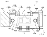
- the power converter 101 of the fifth embodiment includes a plurality (three in FIG. 7) of semiconductor modules 110, a cooler 120, (Two in FIG. 7).
- the case 102 is made of a material having good heat conductivity, that is, a metal material having good so-called “heat drawing”.
- the power converter 101 is mounted on, for example, an electric vehicle or a hybrid vehicle, and is used as an inverter that converts a DC power supply into an AC power required for driving a driving motor. Therefore, the power conversion device 101 is also referred to as an “inverter 101” or an “inverter device 101”.
- the semiconductor module 110 is provided in a power supply path between the power supply 103 which is a DC power supply and the motor 104 which is an AC motor.
- a capacitor 105 having a built-in capacitor element, a PN connector 106 electrically connected to the power supply 103, and a three-phase connector electrically connected to the motor 104 107, a current sensor 109, and a control circuit board 119 (see FIG. 8).
- the semiconductor module 110 includes a main body 111 containing a switching element 114 (see FIG. 8), three power terminals 112, and a plurality of control terminals 113 (see FIG. 8) electrically connected to a control circuit board 119. And a heat radiating unit 115 (see FIG. 8).
- the three power terminals 112 protrude from the main body 111 in parallel in one direction of the third direction Z, and the plurality of control terminals 113 protrude from the main body 111 in parallel with each other in a direction opposite to the power terminals 112. I have.
- the three power terminals 112 of the semiconductor module 110 are classified into a positive terminal 112P, a negative terminal 112N, and an output terminal 112A.
- the positive terminal 112P and the negative terminal 112N are electrically connected via a metal bus bar 116 to a capacitor element (not shown) of the capacitor 105 as a connection device.
- the bus bars 116 are classified into a positive bus bar 116P and a negative bus bar 116N.
- the capacitor 105 is electrically connected to the semiconductor module 110 via the bus bar 116, and is connected to the positive terminal 112P via the positive bus bar 116P and to the negative terminal via the negative bus bar 116N.
- welding is used for the connection between the positive bus bar 116P and the positive terminal 112P, and the connection between the negative bus bar 116N and the negative terminal 112N.
- FIG. 7 illustrates a structure in which three positive bus bars 116P and three negative bus bars 116N protrude from the capacitor 105.
- the three positive bus bars 116P have the same potential, and the three negative bus bars 116N also have the same potential. It is the same potential. Therefore, the three positive bus bars 116P may be configured as one integrated bus bar, and the three negative bus bars 116N may be configured as one integrated bus bar.
- Each of the three output terminals 112A of the three semiconductor modules 110 is electrically connected to the three-phase connector 107 via a metal bus bar 118.
- a metal bus bar 118 For connection between the output terminal 112A and the bus bar 118, welding is used.
- the current flowing through each of the three bus bars 118 is detected by each of the three current sensors 109 held by the wiring holder 108.
- the current sensor 109 is configured as a connection device that is electrically connected to the semiconductor module 110 via the bus bar 118. As shown in FIG. 8, the current sensor 109 is connected to the control circuit board 119, and the detection information is transmitted to the control circuit board 119.
- the control circuit board 119 controls the switching operation (on / off operation) of the switching element 114 built in the main body 111 of the semiconductor module 110 in order to convert the DC power supplied to the semiconductor module 110 into AC power. It is configured as follows. Typically, any switching element such as an IGBT (that is, an insulated gate bipolar transistor) and a MOSFET (that is, a MOS field effect transistor) is used as the switching element 114.
- IGBT that is, an insulated gate bipolar transistor
- MOSFET that is, a MOS field effect transistor
- the capacitor 105 is electrically connected to the PN connector 106 via the metal bus bar 117.
- the bus bars 117 are classified into a positive bus bar 117P and a negative bus bar 117N. Therefore, the capacitor 105 is electrically connected to the positive terminal (not shown) via the positive bus bar 117P and connected to the negative terminal (not shown) via the negative bus bar 117N for connection with the PN connector 106.
- the PN connector 106 is configured as a connection device that is electrically connected to the semiconductor module 110 via the two bus bars 116 and 117 and the capacitor 105.
- the cooler 120 has a plurality of (six in FIG. 7) cooling pipes 123 through which the coolant w flows, and the plurality of cooling pipes 123 are stacked in a first direction X (also referred to as a “stacking direction X”). ) Is configured as a stacked cooler. Two adjacent cooling pipes 123 of the plurality of cooling pipes 123 are arranged with the opposing space S therebetween. In the cooler 120, the coolant w flowing through the inflow pipe 121 flows through the plurality of cooling pipes 123 in parallel in the second direction Y, then merges, and flows out through the outflow pipe 122.
- the cooling module 130 has a function of connecting the condenser 105 and the PN connector 106 to the cooler 120 so as to be able to conduct heat.
- the condenser 105 as the first connection device and the PN connector 106 as the second connection device are respectively arranged on both sides of the cooler 120.
- the cooling module 130 is disposed between the capacitor 105 and the PN connector 106.
- the cooling module 130 includes a metal cooling bus bar 135 capable of conducting heat between the main body 131, the capacitor 105 and the PN connector 106, and a cooler 120.
- a heat radiating part 132 for radiating heat to the heat sink, an electrical insulator 133, and a connection terminal 134 for connecting the cooling bus bar 135 and the heat radiating part 132 are provided.
- the main body 131 is configured as a resin molded part in which a part of the heat radiation part 132 and the connection terminal 134 is buried by the resin material 131a.
- the heat radiating portion 132 has both surfaces in the first direction X exposed from the main body portion 131, and the exposed surface is covered with the electric insulator 133. For this reason, the heat radiating part 132 is configured to be in contact with the cooling pipe 123 of the cooler 120 via the electric insulator 133.
- the cooling bus bars 135 are classified into a first cooling bus bar 135P and a second cooling bus bar 135N.
- the connection terminals 134 protrude from the main body 131 in the same direction as the two power terminals 112 of the semiconductor module 110.
- the connection terminal 134 is disposed near the capacitor 105 and connected to one end of the first cooling bus bar 135P, and the connection terminal 134 is disposed near the PN connector 106 and connected to one end of the second cooling bus bar 135N.
- the second connection terminal 134N is disposed near the capacitor 105 and connected to one end of the first cooling bus bar 135P
- the connection terminal 134 is disposed near the PN connector 106 and connected to one end of the second cooling bus bar 135N.
- the second connection terminal 134N is disposed near the PN connector 106 and connected to one end of the second cooling bus bar 135N.
- connection structure between the connection terminal 134 and the cooling bus bar 135 the same welding as the connection structure between the power terminal 112 of the semiconductor module 110 and the bus bars 116 and 118 is used. Therefore, the first connection terminal 134P is connected to one end of the first cooling bus bar 135P by welding, and the second connection terminal 134N is connected to one end of the second cooling bus bar 135N by welding.
- the first connection terminal 134P is connected to the capacitor 105 via the first cooling bus bar 135P
- the second connection terminal 134N is connected to the PN connector 106 via the second cooling bus bar 135N.
- the first cooling bus bar 135P and the second cooling bus bar 135N form a heat conduction path, and also form a DC current conduction path between the capacitor 105 and the PN connector 106.
- the cooling module 130 has a main body 131 having the same dimensions as the main body 111 of the semiconductor module 110.
- the cooling module 130 has the same thickness as the main body 111 of the semiconductor module 110 in the first direction X (also referred to as the “stacking direction X”), which is the stacking direction of the plurality of cooling pipes 123 (of the facing space S). (A thickness corresponding to the dimension in the first direction X). For this reason, the opposing space S between two adjacent cooling pipes 123 can be used as a space for sandwiching the cooling module 130 from both sides.
- the semiconductor module 110, the cooling module 130, and the cooler 120 form a semiconductor laminated unit.
- this semiconductor laminated unit three semiconductor modules 110 and a plurality of cooling pipes 123 are alternately laminated in the first direction X.
- the semiconductor module 110 is configured such that the heat radiating portion 115 (see FIG. 8) of the main body portion 111 is in contact with the cooling pipe 123 via the same electrical insulator as the electrical insulator 133 in FIG. Have been.
- two cooling modules 130 and a plurality of cooling pipes 123 are alternately stacked in the first direction X.
- each semiconductor module 110 is arranged in the corresponding opposing space S, and is sandwiched by the two cooling pipes 123 from both sides in the first direction X.
- each of the three semiconductor modules 110 is arranged in each of the three opposing spaces S that are consecutively arranged in the first direction X among the five opposing spaces S.
- each of the cooling modules 130 is disposed in the corresponding opposing space S and is sandwiched between the two side surfaces in the first direction X by the two cooling pipes 123.
- each of the two cooling modules 130 is provided in each of the two opposing spaces S that are continuously arranged in the first direction X separately from the opposing space S in which the semiconductor module 110 is disposed among the five opposing spaces S. Is arranged.
- the cooling pipe 123 of the cooler 120 has a function of cooling the cooling module 130 in addition to the function of cooling the semiconductor module 110.
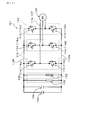
- the inverter circuit of the power conversion device 101 includes three-phase legs. That is, the three-phase legs are connected in parallel to each other on the positive electrode side and the negative electrode side of the power supply 103.
- Each leg is formed by an upper arm switching element 114u and a lower arm switching element 114d connected in series to each other.
- the upper arm switching element 114u and the lower arm switching element 114d are built in the main body 111 of one semiconductor module 110.
- connection point between the upper arm switching element 114u and the lower arm switching element 114d in each leg is connected to the three electrodes of the motor 104 via the bus bar 118 and the three-phase connector 107 (see FIG. 7).
- a flywheel diode is connected to each switching element 114 in anti-parallel.
- the two heat radiating portions 132 of the two cooling modules 130 are connected in parallel to each other on the positive electrode side and the negative electrode side of the power supply 103.
- the cooler 120 has a function of cooling the semiconductor module 110 provided in the power supply path between the power supply 103 and the motor 104.
- the cooling module 130 connects each of the capacitor 105 and the PN connector 106 electrically connected to the semiconductor module 110 via the bus bars 116 and 117 to the cooler 120 so as to be able to conduct heat.
- both the condenser 105 and the PN connector 106 are indirectly cooled using the cooling module 130 cooled by the cooler 120 as a cooling source. That is, the heat of the capacitor 105 and the PN connector 106 is transmitted from the heat radiating portion 132 of the cooling module 130 to the cooler 120 and radiated.
- the cooling function by the cooler 120 is used not only for cooling the semiconductor module 110 but also for cooling the capacitor 105 and the PN connector 106 via the cooling module 130. That is, the cooler 120 is also used for cooling the condenser 105 and the PN connector 106. Therefore, it is not necessary to provide a dedicated cooler for the condenser 105 and the PN connector 106, and it is possible to prevent the entire apparatus from becoming large and from being deteriorated in vehicle mountability.
- a conversion device 101 can be provided. As a result, the life of electronic components such as the capacitor 105 and the PN connector 106 can be extended.
- heat is dissipated by transferring heat from the heat radiating portion 132 of the cooling module 130 to the cooling pipe 123 of the cooler 120.
- the condenser 105 connected to the first cooling bus bar 135P of the cooling module 130 and the PN connector 106 connected to the second cooling bus bar 135N are both cooled.
- the structure of the cooling module 130 for cooling the capacitor 105 and the PN connector 106 can be simplified.
- the cooling module 130 that cools the capacitor 105 and the PN connector 106 using the cooler 120 for the semiconductor module 110 is disposed between the capacitor 105 and the PN connector 106.
- the bus bar length of the first cooling bus bar 135P extending between the first connection terminal 134P and the capacitor 105, and the second cooling bus bar 135N extending between the second connection terminal 134N and the PN connector 106 Busbar length can be kept short.
- connection structure between the connection terminal 134 of the cooling module 130 and the cooling bus bar 135 is the same as the connection structure between the power terminal 112 of the semiconductor module 110 and the bus bars 116, 118, and is matched.
- welding as the connection structure, the number of parts required for connection can be reduced.
- the cooler is installed for installing the cooling module 130.
- This can be dealt with by increasing the number of stacked cooling tubes 123 of 120. In this case, the space required for installing the cooling module 130 can be secured without significantly increasing the size of the cooler 120.
- the size of the opposed space S of the plurality of cooling pipes 123 of the cooler 120 is reduced. Can be kept constant. This can prevent the structure of the cooler 120 from becoming complicated.
- the structure of the cooling module 230 is the same as that of the cooling module 130 in that the cooling module 230 has the first connection terminal 134P and the second connection terminal 134N, and that the cooling module 230 has the heat radiating part 132 (see FIG. 14).
- the structure is different in that a bus bar corresponding to one cooling bus bar 135P is not provided.
- the second connection terminal 134N which is one of the connection terminals 134 of the cooling module 230, is connected to one end of the cooling bus bar 135 by welding.
- the cooling bus bar 135 is connected to three bus bars 118, which are bus bars on the output side of the semiconductor module 110, by a metal bus bar 118A.
- the cooling bus bar 135 is connected to the bus bars 118 and 118A so as to be able to conduct heat, so that the cooling bus bar 135 is connected to the current sensor 109 as a connection device via these bus bars 118 and 118A so as to be able to conduct heat. It is configured to be.
- the cooling bus bar 135 does not form an energization path, but forms only a heat conduction path.
- the cooling module 230 In the cooling module 230, only the second connection terminal 134N is substantially used, so that the first connection terminal 134P can be omitted. On the other hand, when it is necessary to consider the versatility of the connection between the cooling module 230 and various connection devices, the cooling module 230 having the first connection terminal 134P and the second connection terminal 134N is used. Is preferred.
- the cooling module 230 can conduct heat with the current sensor 109 via the cooling bus bar 135 and the bus bars 118 and 118A.
- the power conversion device 201 can improve the cooling performance of the current sensor 109 electrically connected to the semiconductor module 110 via the bus bar 118 without increasing the size of the device.
- the same operation and effect as those of the fifth embodiment are obtained.
- bus bar 118A is connected to at least one of the three bus bars 118, or the bus bar 116 and the bus bar 117 in which the cooling bus bar 135 is replaced or added to the bus bar 118. May be adopted.
- the power converters 101 and 201 each including the three semiconductor modules 110 and the two cooling modules 130 and 230 have been described.
- each of the semiconductor modules 110 and the cooling modules 130 and 230 has the same configuration.
- the numbers are illustrative and can be changed as appropriate as needed.
- the number of cooling pipes 123 of the cooler 120 can be determined according to the numbers of the semiconductor modules 110 and the cooling modules 130 and 230.
- connection terminals 134 of the cooling modules 130 and 230 and the cooling bus bar 135 are connected by welding is exemplified.
- the connection terminals 134 and the cooling bus bar 135 are bolted.
- a structure for connecting by fastening can also be adopted.
- the structure in which the cooling modules 130 and 230 are sandwiched between the two cooling pipes 123 of the cooler 120 has been exemplified.
- the cooling modules 130 and 230 are provided outside the cooler 120. May be adopted.
- the main body 131 of the cooling modules 130 and 230 has the same thickness as the main body 111 of the semiconductor module 110 in the first direction X.
- the dimension in the second direction Y and the dimension in the third direction Z of the main body 131 may be different from that of the main body 111.
- a structure may be employed in which the thickness of the main body 131 of the cooling modules 130 and 230 in the first direction X is different from the thickness of the main body 111 in the first direction X.
- the capacitor 105, the PN connector 106, and the current sensor 109 are exemplified as the connection devices electrically connected to the semiconductor module 110 via the bus bars 116, 117, and 118. And a device such as a reactor can also be employed.
- the stacked cooler 120 that cools the semiconductor module 110 by sandwiching both side surfaces between the two cooling pipes 123 has been described, but the cooler is limited to only the cooler 120. is not.
- a cooler having a structure for cooling one side of the semiconductor module 110 may be employed.
- the semiconductor module 110 is arranged in each of the three continuous opposing spaces S of the five opposing spaces S of the cooler 120, and the cooling module is provided in each of the two continuous opposing spaces S.
- the facing space S in which the semiconductor module 110 and the cooling modules 130 and 230 are arranged is not limited to this, and can be appropriately selected as needed. It is.
- the semiconductor modules 110 and the cooling modules 130 and 230 can be alternately arranged in five opposing spaces S or randomly arranged in five opposing spaces S. Further, the semiconductor module 110 and the cooling modules 130 and 230 can be arranged side by side in one facing space S. Further, an empty facing space S in which neither the semiconductor module 110 nor the cooling modules 130 and 230 are provided may be provided.
- each of the cooling module 120 and the cooling modules 130 and 230 is not limited to this, and can be changed as needed.
Landscapes
- Engineering & Computer Science (AREA)
- Microelectronics & Electronic Packaging (AREA)
- Power Engineering (AREA)
- Physics & Mathematics (AREA)
- Thermal Sciences (AREA)
- Inverter Devices (AREA)
Abstract
Un convertisseur de courant électrique (1) selon la présente invention comprend : un module à semi-conducteurs (2) ; un dispositif de refroidissement (3) qui refroidit le module à semi-conducteurs ; un composant électronique (4) qui est directement ou indirectement connecté au module à semi-conducteurs (2) ; un connecteur haute tension (6) qui est connecté à un dispositif externe ; et des barres omnibus de connexion de connecteur (7) qui connectent le connecteur haute tension (6) et le composant électronique (4) l'un à l'autre. Au moins une des barres omnibus de connexion de connecteur (7) est une barre omnibus de dissipation de chaleur (70) qui est disposée de manière adjacente au dispositif de refroidissement (3).
Priority Applications (1)
| Application Number | Priority Date | Filing Date | Title |
|---|---|---|---|
| CN201980041151.2A CN112313869B (zh) | 2018-06-19 | 2019-05-10 | 电力转换装置 |
Applications Claiming Priority (4)
| Application Number | Priority Date | Filing Date | Title |
|---|---|---|---|
| JP2018-116146 | 2018-06-19 | ||
| JP2018116146A JP6908004B2 (ja) | 2018-06-19 | 2018-06-19 | 電力変換装置 |
| JP2018131741A JP6973313B2 (ja) | 2018-07-11 | 2018-07-11 | 電力変換装置 |
| JP2018-131741 | 2018-07-11 |
Publications (1)
| Publication Number | Publication Date |
|---|---|
| WO2019244502A1 true WO2019244502A1 (fr) | 2019-12-26 |
Family
ID=68982608
Family Applications (1)
| Application Number | Title | Priority Date | Filing Date |
|---|---|---|---|
| PCT/JP2019/018691 Ceased WO2019244502A1 (fr) | 2018-06-19 | 2019-05-10 | Convertisseur de courant électrique |
Country Status (2)
| Country | Link |
|---|---|
| CN (1) | CN112313869B (fr) |
| WO (1) | WO2019244502A1 (fr) |
Cited By (3)
| Publication number | Priority date | Publication date | Assignee | Title |
|---|---|---|---|---|
| JPWO2021149165A1 (fr) * | 2020-01-21 | 2021-07-29 | ||
| WO2022149366A1 (fr) * | 2021-01-08 | 2022-07-14 | 株式会社デンソー | Dispositif de conversion d'énergie électrique |
| CN116133322A (zh) * | 2021-11-15 | 2023-05-16 | 三菱电机株式会社 | 功率转换装置 |
Citations (4)
| Publication number | Priority date | Publication date | Assignee | Title |
|---|---|---|---|---|
| JP2015084609A (ja) * | 2013-10-25 | 2015-04-30 | 三菱電機株式会社 | 接続導体の冷却装置及びそれを用いた電力変換装置 |
| JP2016158358A (ja) * | 2015-02-24 | 2016-09-01 | 株式会社デンソー | 半導体モジュール |
| JP2017153228A (ja) * | 2016-02-24 | 2017-08-31 | アイシン・エィ・ダブリュ株式会社 | インバータ装置 |
| JP2018067998A (ja) * | 2016-10-18 | 2018-04-26 | 三菱電機株式会社 | 電力変換装置 |
Family Cites Families (5)
| Publication number | Priority date | Publication date | Assignee | Title |
|---|---|---|---|---|
| BE565471A (fr) * | 1957-03-08 | |||
| JP5422466B2 (ja) * | 2010-04-01 | 2014-02-19 | 日立オートモティブシステムズ株式会社 | 電力変換装置 |
| JP2013069739A (ja) * | 2011-09-21 | 2013-04-18 | Toyota Motor Corp | 半導体ユニットとその製造方法 |
| JP6039356B2 (ja) * | 2012-10-22 | 2016-12-07 | 日立オートモティブシステムズ株式会社 | 電力変換装置 |
| JP2017017999A (ja) * | 2016-10-27 | 2017-01-19 | 株式会社デンソー | 電力変換装置 |
-
2019
- 2019-05-10 CN CN201980041151.2A patent/CN112313869B/zh active Active
- 2019-05-10 WO PCT/JP2019/018691 patent/WO2019244502A1/fr not_active Ceased
Patent Citations (4)
| Publication number | Priority date | Publication date | Assignee | Title |
|---|---|---|---|---|
| JP2015084609A (ja) * | 2013-10-25 | 2015-04-30 | 三菱電機株式会社 | 接続導体の冷却装置及びそれを用いた電力変換装置 |
| JP2016158358A (ja) * | 2015-02-24 | 2016-09-01 | 株式会社デンソー | 半導体モジュール |
| JP2017153228A (ja) * | 2016-02-24 | 2017-08-31 | アイシン・エィ・ダブリュ株式会社 | インバータ装置 |
| JP2018067998A (ja) * | 2016-10-18 | 2018-04-26 | 三菱電機株式会社 | 電力変換装置 |
Cited By (4)
| Publication number | Priority date | Publication date | Assignee | Title |
|---|---|---|---|---|
| JPWO2021149165A1 (fr) * | 2020-01-21 | 2021-07-29 | ||
| JP7136371B2 (ja) | 2020-01-21 | 2022-09-13 | 株式会社デンソー | 電力変換器 |
| WO2022149366A1 (fr) * | 2021-01-08 | 2022-07-14 | 株式会社デンソー | Dispositif de conversion d'énergie électrique |
| CN116133322A (zh) * | 2021-11-15 | 2023-05-16 | 三菱电机株式会社 | 功率转换装置 |
Also Published As
| Publication number | Publication date |
|---|---|
| CN112313869B (zh) | 2024-08-02 |
| CN112313869A (zh) | 2021-02-02 |
Similar Documents
| Publication | Publication Date | Title |
|---|---|---|
| JP5249365B2 (ja) | 電力変換装置 | |
| JP6409968B2 (ja) | 機電一体型の回転電機装置 | |
| JP6032149B2 (ja) | 電力変換装置 | |
| JP5407275B2 (ja) | 電力変換装置 | |
| KR20180128964A (ko) | 차량 탑재용 전력 변환 장치 | |
| JP6932225B1 (ja) | 電力変換装置 | |
| WO2019208406A1 (fr) | Dispositif de conversion de puissance | |
| JP6908004B2 (ja) | 電力変換装置 | |
| JPWO2015025594A1 (ja) | 電力変換装置 | |
| JP6908061B2 (ja) | 電力変換装置 | |
| JP2019221129A (ja) | 電力変換装置 | |
| CN113329587A (zh) | 电力转换装置 | |
| JP2020184847A (ja) | 電力変換装置 | |
| JP2015100223A (ja) | 電力変換装置 | |
| JP2015053776A (ja) | 電力変換装置 | |
| WO2019244502A1 (fr) | Convertisseur de courant électrique | |
| JP5516187B2 (ja) | 電力変換機 | |
| JP2019122064A (ja) | 電力変換装置 | |
| JP7052609B2 (ja) | 電力変換装置 | |
| JP6973313B2 (ja) | 電力変換装置 | |
| JP4452605B2 (ja) | 半導体装置 | |
| JP5644643B2 (ja) | 負荷駆動装置 | |
| JP5803684B2 (ja) | 電力変換装置 | |
| JP5447191B2 (ja) | 電力変換装置 | |
| US11990799B2 (en) | Capacitor module, inverter module, and motor unit |
Legal Events
| Date | Code | Title | Description |
|---|---|---|---|
| 121 | Ep: the epo has been informed by wipo that ep was designated in this application |
Ref document number: 19822834 Country of ref document: EP Kind code of ref document: A1 |
|
| NENP | Non-entry into the national phase |
Ref country code: DE |
|
| 122 | Ep: pct application non-entry in european phase |
Ref document number: 19822834 Country of ref document: EP Kind code of ref document: A1 |