WO2020003349A1 - Circuit de balayage de fréquence et dispositif radar - Google Patents
Circuit de balayage de fréquence et dispositif radar Download PDFInfo
- Publication number
- WO2020003349A1 WO2020003349A1 PCT/JP2018/023996 JP2018023996W WO2020003349A1 WO 2020003349 A1 WO2020003349 A1 WO 2020003349A1 JP 2018023996 W JP2018023996 W JP 2018023996W WO 2020003349 A1 WO2020003349 A1 WO 2020003349A1
- Authority
- WO
- WIPO (PCT)
- Prior art keywords
- frequency
- division ratio
- frequency division
- signal
- ratio
- Prior art date
- Legal status (The legal status is an assumption and is not a legal conclusion. Google has not performed a legal analysis and makes no representation as to the accuracy of the status listed.)
- Ceased
Links
Images


Classifications
-
- G—PHYSICS
- G01—MEASURING; TESTING
- G01S—RADIO DIRECTION-FINDING; RADIO NAVIGATION; DETERMINING DISTANCE OR VELOCITY BY USE OF RADIO WAVES; LOCATING OR PRESENCE-DETECTING BY USE OF THE REFLECTION OR RERADIATION OF RADIO WAVES; ANALOGOUS ARRANGEMENTS USING OTHER WAVES
- G01S7/00—Details of systems according to groups G01S13/00, G01S15/00, G01S17/00
- G01S7/02—Details of systems according to groups G01S13/00, G01S15/00, G01S17/00 of systems according to group G01S13/00
- G01S7/35—Details of non-pulse systems
-
- G—PHYSICS
- G01—MEASURING; TESTING
- G01S—RADIO DIRECTION-FINDING; RADIO NAVIGATION; DETERMINING DISTANCE OR VELOCITY BY USE OF RADIO WAVES; LOCATING OR PRESENCE-DETECTING BY USE OF THE REFLECTION OR RERADIATION OF RADIO WAVES; ANALOGOUS ARRANGEMENTS USING OTHER WAVES
- G01S13/00—Systems using the reflection or reradiation of radio waves, e.g. radar systems; Analogous systems using reflection or reradiation of waves whose nature or wavelength is irrelevant or unspecified
- G01S13/02—Systems using reflection of radio waves, e.g. primary radar systems; Analogous systems
- G01S13/06—Systems determining position data of a target
- G01S13/08—Systems for measuring distance only
- G01S13/32—Systems for measuring distance only using transmission of continuous waves, whether amplitude-, frequency-, or phase-modulated, or unmodulated
- G01S13/34—Systems for measuring distance only using transmission of continuous waves, whether amplitude-, frequency-, or phase-modulated, or unmodulated using transmission of continuous, frequency-modulated waves while heterodyning the received signal, or a signal derived therefrom, with a locally-generated signal related to the contemporaneously transmitted signal
Definitions
- the present invention relates to a frequency sweep circuit and a radar device using the same.
- Various radar sensors that perform distance measurement and the like using microwaves and millimeter waves employ an FMCW (Frequency Modulated Continuous Wave) method, an FMSK (Frequency Modulated Shift Shift Keying) method, a pulse modulation method, and the like.
- FMCW Frequency Modulated Continuous Wave
- FMSK Frequency Modulated Shift Shift Keying
- Patent Literature 1 in a radar device, a transmission wave having a frequency interval from each other and each having a frequency step and having an output frequency changed stepwise is used in order to improve the accuracy of distance and speed measurement. It is disclosed.
- a PLL Phase Locked Loop
- VCO voltage controlled oscillator
- the present invention aims to solve the above problems.
- a frequency sweep circuit for outputting a plurality of oscillation signals having a frequency interval from each other, comprising: an input terminal to which a reference frequency signal is input; An output terminal connected to the signal, a voltage-controlled oscillator that outputs the output frequency signal based on a phase comparison signal, a frequency divider control circuit that outputs a frequency divider control signal, and the output frequency signal is input, A frequency divider that divides the output frequency signal at a frequency division ratio specified by a frequency divider control signal and outputs a frequency-divided frequency signal, and compares the phases of the reference frequency signal and the frequency-divided frequency signal.
- a phase comparator that outputs the phase comparison signal
- the frequency divider control circuit increases the frequency division ratio from the first frequency division ratio to a second frequency divider that is larger than the first frequency division ratio. Via the circumference ratio, more than the second frequency division ratio After increasing to a third frequency division ratio, the fourth frequency division ratio is smaller than the fourth frequency division ratio and the first frequency division ratio via a fourth frequency division ratio smaller than the third frequency division ratio. Outputting the frequency divider control signal to return the frequency to a fifth frequency division ratio larger than the frequency division ratio, and increasing the frequency division ratio from the second frequency division ratio to the third frequency division ratio.
- the absolute value of the time change rate of the frequency division ratio is smaller than the absolute value of the time change rate of the frequency division ratio when the frequency division ratio increases from the first frequency division ratio to the second frequency division ratio. Is controlled so that
- the frequency division ratio increasing section from the first frequency division ratio to the second frequency division ratio, and the frequency division ratio from the second frequency division ratio to the third frequency division ratio Compared with the increase section, the latter section has a smaller absolute value of the time rate of change of the frequency division ratio, so that transient fluctuation is less likely to occur.
- a frequency sweeping circuit for outputting a plurality of oscillation signals having frequency intervals set to each other, wherein the frequency sweeping circuit is connected to an input terminal to which a reference frequency signal is input and to an output frequency signal.
- Output terminal a voltage controlled oscillator that outputs the output frequency signal based on a phase comparison signal, a frequency divider control circuit that outputs a frequency divider control signal, and the frequency divider that receives the output frequency signal, A frequency divider that divides the output frequency signal by a frequency division ratio specified by a control signal and outputs a frequency-divided frequency signal, and compares the phases of the reference frequency signal and the frequency-divided frequency signal, A phase comparator that outputs a comparison signal, wherein the frequency divider control circuit sets the frequency division ratio from a first frequency division ratio to a second frequency division ratio smaller than the first frequency division ratio.
- a third frequency division ratio smaller than the second frequency division ratio And then, through a fourth frequency division ratio larger than the third frequency division ratio, a fourth frequency division ratio larger than the fourth frequency division ratio and smaller than the first frequency division ratio.
- the frequency divider control signal is output so as to return to the frequency division ratio of 5, and the time change of the frequency division ratio in decreasing the frequency division ratio from the second frequency division ratio to the third frequency division ratio.
- the absolute value of the rate is controlled to be smaller than the absolute value of the time rate of change of the frequency division ratio when the frequency division ratio decreases from the first frequency division ratio to the second frequency division ratio.
- the division interval of the division ratio from the first division ratio to the second division ratio, and the division ratio from the second division ratio to the third division ratio When compared with the decreasing section, the latter section has a smaller absolute value of the time rate of change of the frequency division ratio, so that transient fluctuation is less likely to occur.
- FIG. 2 is a block diagram showing the configuration of the frequency sweep circuit in FIG.
- FIG. 2 is a block diagram showing a detailed configuration example of a frequency divider control circuit in FIG.
- Graph showing ideal time-dependent change of frequency sweep circuit 4 is a graph showing an example of frequency division ratio control corresponding to FIG. 4 when the frequency sweep circuit of FIG. 2 is used.
- 5 is a graph showing an example of a real-time change of the output frequency fvco in the case of the division ratio control of FIG. 5 is a graph showing another example of the division ratio control of FIG. Graph showing an ideal change with time according to another example of the frequency sweep circuit Graph showing an ideal change with time according to another example of the frequency sweep circuit Circuit block diagram of a radar device according to a second embodiment
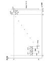
- FIG. 1 is a circuit block diagram of the radar device according to the first embodiment. 1 includes a transmission system 100, a reception system 120, a frequency sweep circuit 150 that outputs a local oscillation signal, and a digital signal processor (DSP) 160 that controls the entire radar device.
- DSP digital signal processor
- the transmission system 100 includes a transmission input 110 that receives a local oscillation signal from the frequency sweep circuit 150, a power amplifier (PA) 101 that amplifies the local oscillation signal received via the transmission input 110 to generate a transmission signal, A transmission antenna 102 for transmitting a transmission signal as an electromagnetic wave toward a target.
- PA power amplifier
- the receiving system 120 includes a receiving input 140 that receives a local oscillation signal from the frequency sweep circuit 150 separately from the transmitting input 110, and a receiving antenna 121 that receives a reflected wave from a target based on the transmitting signal. It has a noise amplifier (LNA) 123, an IQ generation circuit 124, mixers (MIXI, MIXQ) 126 and 127, and an analog-to-digital conversion (ADC) circuit 134.
- LNA noise amplifier
- IQ generation circuit 124 mixers (MIXI, MIXQ) 126 and 127
- ADC analog-to-digital conversion
- IF amplifiers 130 and 131 and filters 132 and 133 are provided.
- FIG. 2 shows the configuration of the frequency sweep circuit 150 in FIG. 2 includes an input terminal 210, a phase comparator 211, a loop filter 212, a voltage controlled oscillator (VCO) 213, a frequency divider 214, a frequency divider control circuit 215, and an output terminal. 216.
- the input terminal 210 receives a reference frequency signal RCLK having a constant reference frequency fref.
- the reference frequency signal RCLK can be supplied from, for example, a crystal oscillator.
- the output terminal 216 is connected to an output frequency signal OUT having a variable output frequency fvco.
- the voltage controlled oscillator 213 outputs an output frequency signal OUT as an oscillation signal based on the phase comparison signal supplied from the phase comparator 211 via the loop filter 212.
- the output frequency signal OUT is provided to the input 110 for transmission and the input 140 for reception as a local oscillation signal.
- the frequency divider control circuit 215 outputs a frequency divider control signal designating the frequency division ratio N.
- the frequency divider 214 receives the output frequency signal OUT, divides the frequency of the output frequency signal OUT by the frequency division ratio N specified by the frequency divider control signal, and generates a frequency-divided frequency signal CCLK having the frequency division frequency fdiv. Output.
- the phase comparator 211 compares the phases of the reference frequency signal RCLK and the divided frequency signal CCLK, and outputs a phase comparison signal.
- the frequency divider control circuit 215 receives the frequency-divided frequency signal CCLK from the frequency divider 214 for timing control. However, the divider control circuit 215 may input the reference frequency signal RCLK instead of the divided frequency signal CCLK.
- fvco fref ⁇ N
- the output frequency fvco changes in proportion to the frequency division ratio N.
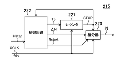
- FIG. 3 shows a detailed configuration example of the frequency divider control circuit 215 in FIG.
- the frequency divider control circuit 215 in FIG. 3 includes an integrator 220, a counter 221, and a control circuit 222.
- the control circuit 222 receives the frequency division ratio interval Nstep between the frequency sequences and sends two signals specifying the initial value Nstart of the frequency division ratio and the increment ⁇ N of the frequency division ratio per clock to the integrator 220.
- a signal designating the length Tc of one sequence of the frequency sequence, which is the time when the increment ⁇ N is to be adopted, is supplied to the counter 221.
- the integrator 220 adds the increment ⁇ N for each clock of the frequency-divided frequency signal CCLK, so that the dividing ratio changes by the increment ⁇ N over time from the initial value Nstart.
- a frequency divider control signal designating N is output.
- the increment ⁇ N is a positive value
- the frequency division ratio N increases with time.
- the increment ⁇ N is a negative value
- the frequency division ratio N decreases with time. If the increment ⁇ N is 0, The frequency division ratio N maintains a constant value.
- the counter 221 counts the number of clocks of the divided frequency signal CCLK, and outputs a count end signal STOP when the count reaches the count corresponding to the set time Tc, that is, when the time Tc has elapsed.
- the control circuit 222 updates the three outputs Nstart, ⁇ N, and Tc.
- the integrator 220 starts the next operation with the updated Nstart and ⁇ N.
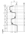
- FIG. 4 is a graph showing an ideal change over time of the output frequency fvco of the frequency sweep circuit 150.
- the period from time t1 to time tx + Tc is an up-chirp period in which the output frequency fvco is increased substantially linearly from the first frequency f1 to the second frequency fx + ⁇ f (f1 ⁇ fx).
- the operation from time t1 to time tx + Tc is repeated.
- the frequency sweep during the up-chirp period is used for distance measurement.
- the number m of frequency sequences from time t1 to time tx + Tc is X.
- a frequency interval fstep (fstep ⁇ f) based on the dividing ratio interval Nstep is set between the frequency sequences. In other words, when the frequency sequence is switched, the frequency interval fstep is added to each frequency value by adding the frequency division ratio interval Nstep to each of the frequency division ratios N in the next frequency sequence.
- Tc1 Tc2
- Tc2 the length up to the switching of the output frequency fvco
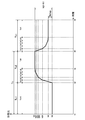
- FIG. 5 is a graph showing an example of frequency division ratio control corresponding to FIG. 4 when the frequency sweep circuit 150 of FIG. 2 is used.
- the third frequency division ratio N3 is continued.
- the length from time t2 to time t5 is Tc2.
- the length from time t5 to time t8 is Tc1.
- the time change rate of the frequency division ratio N in the increase of the frequency division ratio N from the second frequency division ratio N2 to the third frequency division ratio N3 from the time t3 to the time t4 (slope of the graph) Is the time change rate of the frequency division ratio N in the increase of the frequency division ratio N from the first frequency division ratio N1 to the second frequency division ratio N2 between time t2 and time t3 (in the graph, (Slope) is controlled to be smaller than the absolute value.
- the time change rate of the frequency division ratio N in the decrease of the frequency division ratio N from the third frequency division ratio N3 to the fourth frequency division ratio N4 between the time t5 and the time t6 (in the graph, (Slope) is controlled to be smaller than the absolute value.
- FIG. 7 is a graph showing an example of a real-time change of the output frequency fvco in the case of the frequency division ratio control of FIG.
- the absolute value of the time change rate of the frequency division ratio N at the time of increase from the first frequency division ratio N1 to the second frequency division ratio N2 is large.
- Overshoot occurs in the output frequency fvco at the timing of switching from the division ratio N1 of 1 to the second division ratio N2.
- the fluctuation of the output frequency fvco due to the overshoot can be reduced to a predetermined frequency bandwidth (for example, from the first frequency f1 to the third frequency f3). ). Further, the time required for the frequency to stabilize at the time of frequency transition can be reduced.
- the third frequency division is performed.
- An undershoot occurs in the output frequency fvco at the timing of switching from the ratio N3 to the fourth frequency dividing ratio N4.
- the fourth frequency division ratio N4 in anticipation of this transient phenomenon, the fluctuation of the output frequency fvco due to undershoot can be reduced to a predetermined frequency bandwidth (for example, from the third frequency f3 to the first frequency f11). ). Further, the time required for the frequency to stabilize at the time of frequency transition can be reduced.
- the present invention is not limited to this, and may be increased in three or more stages.
- FIG. 8 shows an example in which the frequency division ratio is increased in six stages between time t2 and time t5.
- the absolute value of the time rate of change of the frequency division ratio N is increased each time the frequency increases in the phase where the frequency division ratio N is increased, and every time the level decreases in the phase where the frequency division ratio is decreased. The value is getting smaller. As a result, the amount of overshoot / the amount of undershoot can be further reduced.
- the frequency interval ⁇ f of the output frequency signal OUT in the frequency sequence of the output frequency signal OUT is plus ( ⁇ f> 0).
- the frequency interval ⁇ f of the frequency signal OUT may be minus ( ⁇ f ⁇ 0).
- two output frequency signals OUT having a frequency interval ⁇ f of ⁇ f ( ⁇ f> 0) are output in each frequency series.
- the present invention is not limited to this, and three or more output frequency signals OUT are output.
- the frequency signal OUT may be output.
- FIG. 10 shows an example in which the frequency sweep circuit 150 outputs three output frequency signals OUT having a negative frequency interval ⁇ f ( ⁇ f ⁇ 0) in each frequency series.
- the frequency interval ⁇ f2 ( ⁇ f2 ⁇ 0) between the second output frequency signal OUT (length: Tc2) and the third output frequency signal OUT (length Tc3) may be equal to or different from each other. May be.
- the operation (up-chirp period) from time t1 to time tx + Tc is repeated in frequency sweeping circuit 150, but the present invention is not limited to this.
- the frequency sweeping circuit 150 determines that the output frequency fvco is approximately from the first frequency f1 to the second frequency fx ⁇ f (f1> fx, ⁇ f> 0) within a predetermined period. It may have a characteristic of a down-chirp that decreases linearly, and the down-chirp period may be repeated.
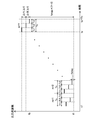
- FIG. 11 is a circuit block diagram of a radar device according to the second embodiment of the present disclosure.
- the radar device in FIG. 11 includes two transmission system circuits 100a and 100b each having the configuration of the transmission system 100 in FIG. 1, and two reception system circuits 120a and 120b each having the configuration of the reception system 120 in FIG. , A frequency sweep circuit 150 that outputs a local oscillation signal, and a DSP 160 that controls the entire radar apparatus.
- the configuration of the frequency sweep circuit 150 can be applied to the same configuration as that shown in FIGS. 2 and 3, and the same effect can be obtained.
- the frequency sweep circuit according to the present invention has an effect of mitigating the adverse effect of the transient fluctuation occurring in the output frequency, and is useful as a frequency sweep circuit or the like for a distance measurement sensor.
- Frequency sweep circuit 210 Input terminal 211 Phase comparator 213 Voltage controlled oscillator (VCO) 214 frequency divider 215 frequency divider control circuit 216 output terminal
- VCO Voltage controlled oscillator
Landscapes
- Engineering & Computer Science (AREA)
- Radar, Positioning & Navigation (AREA)
- Remote Sensing (AREA)
- Computer Networks & Wireless Communication (AREA)
- Physics & Mathematics (AREA)
- General Physics & Mathematics (AREA)
- Radar Systems Or Details Thereof (AREA)
Abstract
Un circuit de commande de diviseur de fréquence (215) délivre en sortie un signal de commande de division de fréquence de telle sorte qu'un rapport de division de fréquence est amené à augmenter d'un premier rapport de division de fréquence, en passant par un deuxième rapport de division de fréquence plus grand que le premier rapport de division de fréquence, à un troisième rapport de division de fréquence plus grand que le deuxième rapport de division de fréquence, puis le rapport de division de fréquence est renvoyé du troisième rapport de division de fréquence, en passant par un quatrième rapport de division de fréquence plus petit que le troisième rapport de division de fréquence, à un cinquième rapport de division de fréquence qui est plus petit que le quatrième rapport de division de fréquence et plus grand que le premier rapport de division de fréquence. De plus, une commande est effectuée de telle sorte que la valeur absolue d'un taux de variation dans le temps du rapport de division de fréquence pendant l'augmentation du deuxième rapport de division de fréquence au troisième rapport de division de fréquence est inférieure à la valeur absolue d'un taux de variation dans le temps du rapport de division de fréquence pendant l'augmentation du premier rapport de division de fréquence au deuxième rapport de division de fréquence.
Priority Applications (3)
| Application Number | Priority Date | Filing Date | Title |
|---|---|---|---|
| PCT/JP2018/023996 WO2020003349A1 (fr) | 2018-06-25 | 2018-06-25 | Circuit de balayage de fréquence et dispositif radar |
| JP2020526729A JPWO2020003349A1 (ja) | 2018-06-25 | 2018-06-25 | 周波数掃引回路およびレーダー装置 |
| US17/119,639 US11846720B2 (en) | 2018-06-25 | 2020-12-11 | Frequency sweep circuit and radar device |
Applications Claiming Priority (1)
| Application Number | Priority Date | Filing Date | Title |
|---|---|---|---|
| PCT/JP2018/023996 WO2020003349A1 (fr) | 2018-06-25 | 2018-06-25 | Circuit de balayage de fréquence et dispositif radar |
Related Child Applications (1)
| Application Number | Title | Priority Date | Filing Date |
|---|---|---|---|
| US17/119,639 Continuation US11846720B2 (en) | 2018-06-25 | 2020-12-11 | Frequency sweep circuit and radar device |
Publications (1)
| Publication Number | Publication Date |
|---|---|
| WO2020003349A1 true WO2020003349A1 (fr) | 2020-01-02 |
Family
ID=68986150
Family Applications (1)
| Application Number | Title | Priority Date | Filing Date |
|---|---|---|---|
| PCT/JP2018/023996 Ceased WO2020003349A1 (fr) | 2018-06-25 | 2018-06-25 | Circuit de balayage de fréquence et dispositif radar |
Country Status (3)
| Country | Link |
|---|---|
| US (1) | US11846720B2 (fr) |
| JP (1) | JPWO2020003349A1 (fr) |
| WO (1) | WO2020003349A1 (fr) |
Citations (2)
| Publication number | Priority date | Publication date | Assignee | Title |
|---|---|---|---|---|
| JP2009194428A (ja) * | 2008-02-12 | 2009-08-27 | Panasonic Corp | シンセサイザと、これを用いた受信装置、および電子機器 |
| WO2017056287A1 (fr) * | 2015-10-01 | 2017-04-06 | 三菱電機株式会社 | Générateur de signal de compression d'impulsions linéaire |
Family Cites Families (35)
| Publication number | Priority date | Publication date | Assignee | Title |
|---|---|---|---|---|
| FR2754604B1 (fr) * | 1992-06-05 | 1999-04-09 | Thomson Csf | Dispositif de linearisation d'une rampe de modulation de frequence et son application a un radio-altimetre |
| DE19922411A1 (de) * | 1999-04-07 | 2000-10-12 | Volkswagen Ag | Radarverfahren zur Messung von Abständen und Relativgeschwindigkeiten zwischen einem Fahrzeug und einem oder mehreren Hindernissen |
| US6114987A (en) * | 1999-05-29 | 2000-09-05 | Sensor Technologies & Systems, Inc. | Dual-loop linearizer for FM-CW radar |
| US6577269B2 (en) * | 2000-08-16 | 2003-06-10 | Raytheon Company | Radar detection method and apparatus |
| DE10050278B4 (de) * | 2000-10-10 | 2005-06-02 | S.M.S., Smart Microwave Sensors Gmbh | Verfahren und Vorrichtung zur Bestimmung von Abstand und Relativgeschwindigkeit eines entfernten Objektes |
| JP3988571B2 (ja) * | 2001-09-17 | 2007-10-10 | 株式会社デンソー | レーダ装置 |
| DE10231597A1 (de) * | 2002-07-12 | 2004-01-29 | Robert Bosch Gmbh | Verfahren und Radarsystem zur Bestimmung der Richtungswinkel von Radarobjekten |
| DE102005008715A1 (de) * | 2005-02-25 | 2006-08-31 | Robert Bosch Gmbh | Radarsystem für Kraftfahrzeuge |
| US7898344B2 (en) * | 2006-09-12 | 2011-03-01 | Fujitsu Limited | Phase-locked oscillator and multi-radar system using same |
| JP4977443B2 (ja) * | 2006-10-31 | 2012-07-18 | 日立オートモティブシステムズ株式会社 | レーダ装置及びレーダ検出方法 |
| JP4871104B2 (ja) * | 2006-11-24 | 2012-02-08 | 日立オートモティブシステムズ株式会社 | レーダ装置及び信号処理方法 |
| DE102007043535A1 (de) * | 2007-09-12 | 2009-03-19 | Robert Bosch Gmbh | FMCW-Radarortungsvorrichtung und entsprechendes FMCW-Radarortungsverfahren |
| WO2009101792A1 (fr) * | 2008-02-12 | 2009-08-20 | Panasonic Corporation | Synthétiseur et dispositif de réception l'utilisant |
| GB2462148A (en) * | 2008-07-31 | 2010-02-03 | Mitsubishi Electric Inf Tech | Automotive FMCW radar with multiple frequency chirps |
| EP2396887A4 (fr) * | 2009-02-13 | 2012-08-29 | Freescale Semiconductor Inc | Circuit intégré comprenant une circuiterie de génération de fréquence pour commander une source de fréquence |
| DE102009001265A1 (de) * | 2009-03-02 | 2010-09-09 | Robert Bosch Gmbh | Radarsensor mit Blinheitserkennungseinrichtung |
| DE102012102185A1 (de) * | 2011-03-16 | 2012-09-27 | Electronics And Telecommunications Research Institute | Radarvorrichtung, die den kurz- und langreichweitigen Radarbetrieb unterstützt |
| US9024809B2 (en) * | 2011-03-17 | 2015-05-05 | Sony Corporation | Object detection system and method |
| DE102013200951A1 (de) * | 2013-01-22 | 2014-07-24 | Robert Bosch Gmbh | FMCW-Radar mit Abstandsbereichseinteilung |
| KR102204839B1 (ko) * | 2014-02-11 | 2021-01-19 | 한국전자통신연구원 | 레이더를 이용한 표적 검출 장치 및 표적을 검출하는 방법 |
| US9219487B1 (en) * | 2014-08-29 | 2015-12-22 | Infineon Technologies Ag | Frequency ramp generation in PLL based RF frontend |
| JP6381656B2 (ja) * | 2014-10-03 | 2018-08-29 | 三菱電機株式会社 | 信号生成回路 |
| KR102202600B1 (ko) * | 2014-11-10 | 2021-01-13 | 한국전자통신연구원 | 레이더 신호 처리를 위한 빔 형성 장치 및 그 방법 |
| US9885781B2 (en) * | 2015-04-08 | 2018-02-06 | Richwave Technology Corp. | Detector generating a displacement signal by injection locking and injection pulling |
| JP6481502B2 (ja) * | 2015-05-18 | 2019-03-13 | 富士通株式会社 | ロック検出回路、発振源回路および無線機器 |
| EP3096160B1 (fr) * | 2015-05-20 | 2020-02-26 | Veoneer Sweden AB | Système radar de véhicule fmcw |
| KR101760907B1 (ko) * | 2015-11-20 | 2017-07-24 | 주식회사 만도 | 차량용 레이더 장치 및 그의 타겟 측정 방법 |
| EP3316484A1 (fr) * | 2016-10-27 | 2018-05-02 | NXP USA, Inc. | Synthétiseur numérique, unité de communication et procédé associé |
| EP3316483A1 (fr) * | 2016-10-27 | 2018-05-02 | NXP USA, Inc. | Synthétiseur numérique, unité de communication et procédé associé |
| DE102017124343B4 (de) * | 2016-12-16 | 2021-04-08 | Infineon Technologies Ag | Erzeugung schneller frequenzrampen |
| DE102017200706A1 (de) * | 2017-01-18 | 2018-07-19 | Robert Bosch Gmbh | Mehrfach unterabgetastetes Chirp-Sequence-Radar |
| EP3401652B1 (fr) * | 2017-05-09 | 2020-08-12 | VEGA Grieshaber KG | Jauge radar équipée d'une boucle à verrouillage de phase |
| DE102017113730A1 (de) * | 2017-06-21 | 2018-12-27 | Infineon Technologies Ag | Radar-frontend mit hf-oszillator-überwachung |
| US10955547B2 (en) * | 2018-05-24 | 2021-03-23 | The Boeing Company | Combined radar and communications system using common signal waveform |
| US11360215B2 (en) * | 2018-12-20 | 2022-06-14 | Gm Cruise Holdings Llc | Lidar system that is configured to compute ranges with differing range resolutions |
-
2018
- 2018-06-25 WO PCT/JP2018/023996 patent/WO2020003349A1/fr not_active Ceased
- 2018-06-25 JP JP2020526729A patent/JPWO2020003349A1/ja active Pending
-
2020
- 2020-12-11 US US17/119,639 patent/US11846720B2/en active Active
Patent Citations (2)
| Publication number | Priority date | Publication date | Assignee | Title |
|---|---|---|---|---|
| JP2009194428A (ja) * | 2008-02-12 | 2009-08-27 | Panasonic Corp | シンセサイザと、これを用いた受信装置、および電子機器 |
| WO2017056287A1 (fr) * | 2015-10-01 | 2017-04-06 | 三菱電機株式会社 | Générateur de signal de compression d'impulsions linéaire |
Also Published As
| Publication number | Publication date |
|---|---|
| JPWO2020003349A1 (ja) | 2021-06-24 |
| US20210096212A1 (en) | 2021-04-01 |
| US11846720B2 (en) | 2023-12-19 |
Similar Documents
| Publication | Publication Date | Title |
|---|---|---|
| US10819349B2 (en) | Parallel fractional-N phase locked loop circuit | |
| US7619558B2 (en) | Clock pulse control device of a microwave pulse radar | |
| US10444338B2 (en) | Transmitter-receiver system | |
| EP2495634B1 (fr) | Générateur à base de temps et procédé de fourniture d'un premier signal d'horloge et d'un deuxième signal d'horloge | |
| EP3493405A2 (fr) | Synthétiseur de signal à chirp utilisant des plls | |
| US8723577B2 (en) | Spreading a clock signal | |
| US20180267159A1 (en) | Signal generator | |
| US8207762B2 (en) | Digital time base generator and method for providing a first clock signal and a second clock signal | |
| US20190305781A1 (en) | Pll circuit | |
| CN114679174B (zh) | 用于毫米波应用的高性能锁相环 | |
| US9722659B2 (en) | Frequency ramp generation | |
| US10530373B1 (en) | Method and system for generating a saw-tooth signal with fast fly back interval | |
| CN109085543B (zh) | 线性调频信号发生器 | |
| US10935631B2 (en) | Radar transceiver with a switched local oscillator | |
| US20170366193A1 (en) | Programmable frequency divider, pll synthesizer and radar device | |
| El-Shennawy et al. | Fractional-N PLL optimization for highly linear wideband chirp generation for FMCW radars | |
| JP3091423B2 (ja) | 正確なデジタル位相シフタ | |
| WO2020003349A1 (fr) | Circuit de balayage de fréquence et dispositif radar | |
| US11088697B2 (en) | PLL circuit | |
| Ali et al. | Design and implementation of FMCW radar using the raspberry Pi single board computer | |
| CN109873638B (zh) | 一种提高相位分辨率的参考移相器及移相方法 | |
| EP1882194B1 (fr) | Dispositif de commande de signal d'horloge d'un radar de signal hyperfrequence | |
| WO2021150505A1 (fr) | Saut de fréquence multicanal synchrone de signaux modulés | |
| WO2001063742A1 (fr) | Boucle a phase asservie pour balayage de frequence | |
| TWI527380B (zh) | 頻率鎖定裝置 |
Legal Events
| Date | Code | Title | Description |
|---|---|---|---|
| 121 | Ep: the epo has been informed by wipo that ep was designated in this application |
Ref document number: 18923821 Country of ref document: EP Kind code of ref document: A1 |
|
| ENP | Entry into the national phase |
Ref document number: 2020526729 Country of ref document: JP Kind code of ref document: A |
|
| NENP | Non-entry into the national phase |
Ref country code: DE |
|
| 122 | Ep: pct application non-entry in european phase |
Ref document number: 18923821 Country of ref document: EP Kind code of ref document: A1 |