WO2020003568A1 - Étiquette rfid et matériau attaché à un rfid - Google Patents
Étiquette rfid et matériau attaché à un rfid Download PDFInfo
- Publication number
- WO2020003568A1 WO2020003568A1 PCT/JP2019/002003 JP2019002003W WO2020003568A1 WO 2020003568 A1 WO2020003568 A1 WO 2020003568A1 JP 2019002003 W JP2019002003 W JP 2019002003W WO 2020003568 A1 WO2020003568 A1 WO 2020003568A1
- Authority
- WO
- WIPO (PCT)
- Prior art keywords
- insulating substrate
- mounting surface
- rfid tag
- coiled antenna
- antenna
- Prior art date
- Legal status (The legal status is an assumption and is not a legal conclusion. Google has not performed a legal analysis and makes no representation as to the accuracy of the status listed.)
- Ceased
Links
Images




Classifications
-
- G—PHYSICS
- G06—COMPUTING OR CALCULATING; COUNTING
- G06K—GRAPHICAL DATA READING; PRESENTATION OF DATA; RECORD CARRIERS; HANDLING RECORD CARRIERS
- G06K19/00—Record carriers for use with machines and with at least a part designed to carry digital markings
- G06K19/06—Record carriers for use with machines and with at least a part designed to carry digital markings characterised by the kind of the digital marking, e.g. shape, nature, code
- G06K19/067—Record carriers with conductive marks, printed circuits or semiconductor circuit elements, e.g. credit or identity cards also with resonating or responding marks without active components
- G06K19/07—Record carriers with conductive marks, printed circuits or semiconductor circuit elements, e.g. credit or identity cards also with resonating or responding marks without active components with integrated circuit chips
- G06K19/077—Constructional details, e.g. mounting of circuits in the carrier
- G06K19/07749—Constructional details, e.g. mounting of circuits in the carrier the record carrier being capable of non-contact communication, e.g. constructional details of the antenna of a non-contact smart card
- G06K19/07773—Antenna details
- G06K19/07792—Antenna details the antenna adapted for extending in three dimensions
-
- G—PHYSICS
- G06—COMPUTING OR CALCULATING; COUNTING
- G06K—GRAPHICAL DATA READING; PRESENTATION OF DATA; RECORD CARRIERS; HANDLING RECORD CARRIERS
- G06K19/00—Record carriers for use with machines and with at least a part designed to carry digital markings
- G06K19/06—Record carriers for use with machines and with at least a part designed to carry digital markings characterised by the kind of the digital marking, e.g. shape, nature, code
- G06K19/067—Record carriers with conductive marks, printed circuits or semiconductor circuit elements, e.g. credit or identity cards also with resonating or responding marks without active components
- G06K19/07—Record carriers with conductive marks, printed circuits or semiconductor circuit elements, e.g. credit or identity cards also with resonating or responding marks without active components with integrated circuit chips
- G06K19/077—Constructional details, e.g. mounting of circuits in the carrier
- G06K19/07749—Constructional details, e.g. mounting of circuits in the carrier the record carrier being capable of non-contact communication, e.g. constructional details of the antenna of a non-contact smart card
- G06K19/07773—Antenna details
- G06K19/07777—Antenna details the antenna being of the inductive type
- G06K19/07784—Antenna details the antenna being of the inductive type the inductive antenna consisting of a plurality of coils stacked on top of one another
-
- H—ELECTRICITY
- H01—ELECTRIC ELEMENTS
- H01Q—ANTENNAS, i.e. RADIO AERIALS
- H01Q1/00—Details of, or arrangements associated with, antennas
- H01Q1/12—Supports; Mounting means
- H01Q1/22—Supports; Mounting means by structural association with other equipment or articles
- H01Q1/2208—Supports; Mounting means by structural association with other equipment or articles associated with components used in interrogation type services, i.e. in systems for information exchange between an interrogator/reader and a tag/transponder, e.g. in Radio Frequency Identification [RFID] systems
- H01Q1/2225—Supports; Mounting means by structural association with other equipment or articles associated with components used in interrogation type services, i.e. in systems for information exchange between an interrogator/reader and a tag/transponder, e.g. in Radio Frequency Identification [RFID] systems used in active tags, i.e. provided with its own power source or in passive tags, i.e. deriving power from RF signal
-
- H—ELECTRICITY
- H01—ELECTRIC ELEMENTS
- H01Q—ANTENNAS, i.e. RADIO AERIALS
- H01Q7/00—Loop antennas with a substantially uniform current distribution around the loop and having a directional radiation pattern in a plane perpendicular to the plane of the loop
Definitions
- the present invention relates to an RFID (Radio-Frequency @ IDentification) tag and an article with RFID.
- an RFID tag having a structure in which an RFIC (Radio-Frequency Integrated Circuit) element is mounted on a mounting surface of a substrate having a coiled antenna built therein is known.
- the winding axis of the coil antenna is provided perpendicular to the mounting surface of the substrate.
- Patent Literature 1 discloses an RFID tag configured such that the center of the coiled antenna in the winding axis direction is farther from the metal surface than the center of the substrate. According to the RFID tag disclosed in Patent Literature 1, by disposing the coiled antenna away from the metal surface, it is possible to suppress the influence from the metal surface and to suppress a decrease in the communication distance of the RFID tag.
- An object of the present invention is to solve the above-described problems and to provide an RFID tag and an article with an RFID tag that can further suppress a decrease in communication distance due to a metal surface.
- an RFID tag includes: An RFIC element; A first insulating substrate having a mounting surface on which the RFIC element is mounted, and a first coiled antenna built in the first insulating substrate and having a winding axis in a direction orthogonal or substantially orthogonal to the mounting surface.
- a first inductor element provided; A second insulating substrate mounted on the mounting surface; a second insulating substrate built in the second insulating substrate, electrically connected to the first coiled antenna, and wound parallel or substantially parallel to the mounting surface.
- a second inductor element comprising: a second coiled antenna having an axis;
- the first insulating substrate is configured by a laminate in which a plurality of dielectric layers or magnetic layers are laminated,
- the first coil antenna is configured by a laminated coil antenna in which coil conductor patterns formed on each layer of the laminate are connected.
- the article with the RFID tag includes: An article having a metal surface; An RFID tag attached to the metal surface; An article with an RFID tag comprising: The RFID tag, An RFIC element; A first insulating substrate facing the metal surface at a position distant from the metal surface and having a mounting surface on which the RFIC element is mounted; and a direction embedded in the first insulating substrate and orthogonal or substantially orthogonal to the mounting surface.
- a first inductor element comprising: a first coiled antenna having a winding axis on the first inductor element; A second insulating substrate mounted on the mounting surface; a second insulating substrate built in the second insulating substrate, electrically connected to the first coiled antenna, and wound parallel or substantially parallel to the mounting surface.
- a second inductor element comprising: a second coiled antenna having an axis; With The first insulating substrate is configured by a laminate in which a plurality of dielectric layers or magnetic layers are laminated, The first coil antenna is configured by a laminated coil antenna in which coil conductor patterns formed on each layer of the laminate are connected.
- a reduction in the communication distance due to the metal surface can be further suppressed.
- FIG. 2 is a bottom view of the RFID tag of FIG.
- FIG. 2 is a bottom view illustrating a configuration example of a first inductor element included in the RFID tag of FIG. 1.
- FIG. 2 is a bottom view illustrating a configuration example of a first inductor element included in the RFID tag of FIG. 1.
- FIG. 2 is a bottom view illustrating a configuration example of a first inductor element included in the RFID tag of FIG. 1.
- FIG. 2 is a perspective view showing the inside of a second inductor element included in the RFID tag of FIG. 1.
- FIG. 2 is an equivalent circuit diagram of the RFID tag of FIG. 1.
- FIG. 1 is an equivalent circuit diagram of the RFID tag of FIG. 1.
- FIG. 2 is a side view showing how wireless communication is performed between the RFID tag of FIG. 1 and a reader / writer of the RFID system.
- a vertical cross-sectional view showing a state in which a part of the magnetic field flowing in the winding axis direction in the opening area of the first coiled antenna reflects on the RFIC element and flows to the opening area of the second coiled antenna.
- FIG. 2 is a vertical cross-sectional view showing how wireless communication is performed between the RFID tag of FIG. 1 and a reader / writer of the RFID system.
- FIG. 4 is a bottom view showing a modification of the RFID tag of FIG. 1.
- An RFID tag includes: An RFIC element; A first insulating substrate having a mounting surface on which the RFIC element is mounted, and a first coiled antenna built in the first insulating substrate and having a winding axis in a direction orthogonal or substantially orthogonal to the mounting surface.
- a first inductor element provided; A second insulating substrate mounted on the mounting surface; a second insulating substrate built in the second insulating substrate, electrically connected to the first coiled antenna, and wound parallel or substantially parallel to the mounting surface.
- a second inductor element comprising: a second coiled antenna having an axis;
- the first insulating substrate is configured by a laminate in which a plurality of dielectric layers or magnetic layers are laminated,
- the first coil antenna is configured by a laminated coil antenna in which coil conductor patterns formed on each layer of the laminate are connected.
- the RFID tag by mounting the RFID tag such that the second inductor element is close to the metal surface and the first inductor element is separated from the metal surface, it is possible to further suppress a reduction in the communication distance due to the metal surface. That is, since the winding axis of the second coiled antenna is provided parallel or substantially parallel to the mounting surface, the magnetic field flowing in the direction of the winding axis through the opening area of the second coiled antenna is not affected by the metal surface. Can be reduced. Further, since the first inductor element is arranged away from the metal surface, the influence from the metal surface can be suppressed.
- the first insulating substrate with a laminated body and configuring the first coiled antenna with a laminated coiled antenna, it is easy to generate a strong magnetic field on the mounting surface side and the opposite surface side (magnetic field arrival direction). can do. Thereby, the first coiled antenna and the second coiled antenna can operate more effectively. As a result, a reduction in the communication distance due to the metal surface can be further suppressed. Also, since the winding axis of the second coiled antenna is provided parallel or substantially parallel to the mounting surface, for example, a magnetic field caused by an eddy current generated on a metal surface by a high frequency signal radiated from the antenna of the reader / writer Is received by the second coiled antenna. Thus, even if the opening area of the antenna of the reader / writer does not overlap with the opening area of the first coiled antenna, the antenna of the reader / writer and the RFID tag can communicate with each other.
- the RFIC element and the second inductor element may be located in the opening area of the first coiled antenna when viewed from the direction of the winding axis of the first coiled antenna. According to this structure, the size of the RFID tag can be reduced.
- the RFIC element and the second inductor element may be arranged on the mounting surface at an interval from each other. According to this configuration, it is possible for the magnetic field that flows in the opening area of the first coiled antenna in the winding axis direction and is reflected on the RFIC element to flow to the opening area of the second coiled antenna. As a result, it is possible to make the second coil antenna work more effectively, and to make the communication distance of the RFID tag longer.
- the plurality of second inductor elements may be mounted on the mounting surface, and the plurality of second inductor elements may be arranged such that the winding axis directions of the second coiled antennas cross each other. Good. According to this configuration, the magnetic field due to the eddy current generated on the metal surface can be more reliably received by any of the second coiled antennas. As a result, it is possible to make the second coil antenna work more effectively, and to make the communication distance of the RFID tag longer.
- the height of the second inductor element from the mounting surface may be higher than the height of the RFIC element from the mounting surface. According to this configuration, it is possible to suppress the RFIC element from obstructing the flow of the magnetic field due to the eddy current generated on the metal surface to the opening region of the second coiled antenna.
- a resin member may be formed on the mounting surface of the first insulating substrate so as to seal the RFIC element and the second inductor element. It is possible to suppress the occurrence of problems such as short-circuit due to wetness of the mounting portion of the RFIC element and the second inductor element with the first insulating substrate, and to improve the strength of the RFID tag.
- the first coil antenna and the second coil antenna may be antennas that perform wireless communication in a UHF band. According to this configuration, a stronger magnetic field can be more easily generated on the mounting surface side and the opposite surface side (magnetic field arrival direction), and the first coil antenna and the second coil antenna operate more effectively. be able to. As a result, a reduction in the communication distance due to the metal surface can be further suppressed.
- Articles with an RFID tag include: An article having a metal surface; An RFID tag attached to the metal surface; An article with an RFID tag comprising: The RFID tag, An RFIC element; A first insulating substrate facing the metal surface at a position distant from the metal surface and having a mounting surface on which the RFIC element is mounted; and a direction embedded in the first insulating substrate and orthogonal or substantially orthogonal to the mounting surface.
- a first inductor element comprising: a first coiled antenna having a winding axis; A second insulating substrate mounted on the mounting surface; a second insulating substrate built in the second insulating substrate, electrically connected to the first coiled antenna, and wound parallel or substantially parallel to the mounting surface.
- a second inductor element comprising: a second coiled antenna having an axis;
- the first insulating substrate is configured by a laminate in which a plurality of dielectric layers or magnetic layers are laminated,
- the first coiled antenna is constituted by a laminated coiled antenna in which conductor patterns formed on each layer of the laminate are connected.
- the RFID tag is attached so that the second inductor element is closer to the metal surface than the first inductor element, it is possible to further suppress a reduction in the communication distance due to the metal surface. That is, since the winding axis of the second coiled antenna is provided parallel or substantially parallel to the mounting surface, the magnetic field flowing in the direction of the winding axis through the opening area of the second coiled antenna is not affected by the metal surface. Can be reduced. Further, since the first inductor element is disposed apart from the metal surface, the influence from the metal surface can be suppressed.
- the first insulating substrate with a laminated body and configuring the first coiled antenna with a laminated coiled antenna, it is easy to generate a strong magnetic field on the mounting surface side and the opposite surface side (magnetic field arrival direction). can do. Thereby, the first coiled antenna and the second coiled antenna can operate more effectively. As a result, a reduction in the communication distance due to the metal surface can be further suppressed. Further, since the winding axis of the second coiled antenna is provided parallel or substantially parallel to the mounting surface, the flow of magnetic flux passing through the opening area of the second coiled antenna in the winding axis direction is caused by the metal surface. The inhibition can be suppressed.
- the second coil antenna can receive a magnetic field due to an eddy current generated on the metal surface by a high-frequency signal radiated from the antenna of the reader / writer.
- the antenna of the reader / writer and the RFID tag can communicate with each other.
- FIG. 1 is a longitudinal sectional view illustrating a schematic configuration of an article with an RFID tag including the RFID tag according to the embodiment of the present invention.
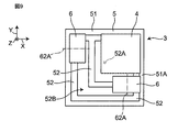
- FIG. 2 is a bottom view of the RFID tag of FIG.
- an article 1 with an RFID (Radio-Frequency IDentification) tag includes an article 2 having a metal surface 2A and an RFID tag 3 attached to the metal surface 2A.
- the RFID tag 3 is electrically attached to the metal surface 2A via, for example, solder or an anisotropic conductive paste (ACP) or by capacitive coupling.
- the RFID tag 3 includes an RFIC (Radio-Frequency Integrated Circuit) element 4, a first inductor element 5, and two second inductor elements 6.
- RFIC Radio-Frequency Integrated Circuit
- the RFIC element 4 is a chip-shaped component that processes a transmission / reception signal of a predetermined frequency (for example, UHF band, HF band).
- the RFIC element 4 is an RFIC chip corresponding to a communication frequency in the UHF band (860 MHz to 960 MHz).
- the RFIC element 4 in plan view (when viewed from the Z direction), has a size included in the first inductor element 5, that is, a size smaller than the first inductor element 5.
- the RFIC element 4 has, for example, a size of 0.45 mm in the X direction, 0.45 mm in the Y direction, and 0.1 mm in the Z direction.
- the RFID element 4 is electrically attached to the first inductor element 5 via, for example, solder or an anisotropic conductive paste (ACP).
- ACP anisotropic conductive paste
- the first inductor element 5 includes a first insulating substrate 51 and a first coiled antenna 52 built in the first insulating substrate 51.
- the first inductor element 5 is a chip-shaped component (chip inductor).
- the first insulating substrate 51 is a substrate that has a mounting surface 51A that faces the metal surface 2A at a position distant from the metal surface 2A and on which the RFIC element 4 is mounted.
- the first insulating substrate 51 is configured by a laminate in which a plurality of dielectric layers or magnetic layers are laminated.
- the first insulating substrate 51 is, for example, a ceramic laminate.
- the first insulating substrate 51 has, for example, a size of 1.2 mm in the X direction, 1.2 mm in the Y direction, and 0.2 mm in the Z direction.
- the first coiled antenna 52 is a linear antenna conductor wound in a coil around the winding axis 52A.
- the first coiled antenna 52 is an antenna that performs wireless communication in the UHF band.
- the first coiled antenna 52 has a winding axis 52A in a direction (Z direction) orthogonal or substantially orthogonal to the mounting surface 51A.
- a part of the RFIC element 4 is located in the opening area 52B of the first coiled antenna 52.
- the first coiled antenna 52 has, for example, a size of 0.8 mm in the X direction, 0.8 mm in the Y direction, and 0.164 mm in the Z direction.
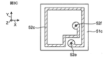
- FIGS. 3A to 3C are bottom views showing a configuration example of the first inductor element 5.
- FIG. 3A to 3C are bottom views showing a configuration example of the first inductor element 5.
- the first insulating substrate 51 is formed by stacking three layers 51a, 51b, and 51c shown in FIGS. 3A to 3C.
- the first coiled antenna 52 is constituted by a laminated coiled antenna in which coil conductor patterns 52a, 52b, 52c formed on the respective layers 51a, 51b, 51c are connected by interlayer connection conductors 52d, 52e, 52f.
- One end of the first coiled antenna 52 is electrically connected to one input / output terminal (not shown) of the RFIC element 4.
- the other end of the first coiled antenna 52 is electrically connected to the other input / output terminal (not shown) of the RFIC element 4.
- two second inductor elements 6 are mounted on the mounting surface 51 ⁇ / b> A of the first insulating substrate 51.
- the RFIC element 4 and the two second inductor elements 6 are arranged on the mounting surface 51A with an interval (for example, 0.125 mm or more) therebetween.
- the second inductor element 6 in plan view (when viewed from the Z direction), has a size included in the first inductor element 5, that is, a size smaller than the first inductor element 5. ing.
- the second inductor element 6 is electrically attached to the first inductor element 5 via, for example, solder or an anisotropic conductive paste (ACP).
- the height (length in the Z direction) of the second inductor element 6 from the mounting surface 51A is designed to be higher than the height of the RFIC element 4 from the mounting surface 51A.
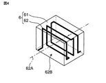
- FIG. 4 is a perspective view showing the inside of the second inductor element 6 in a see-through manner.
- the second inductor element 6 includes a second insulating substrate 61 and a second coiled antenna 62 built in the second insulating substrate 61.
- the second inductor element 6 is a chip-shaped component (chip inductor).
- the second insulating substrate 61 is a substrate mounted on the mounting surface 51A of the first insulating substrate 51.
- the second insulating substrate 61 is configured by a laminate in which a plurality of dielectric layers or magnetic layers are laminated.
- the second insulating substrate 61 is, for example, a ceramic laminate.
- the second insulating substrate 61 has, for example, a size of 0.2 mm in the X direction, 0.4 mm in the Y direction, and 0.3 mm in the Z direction.
- the second coiled antenna 62 is a linear antenna conductor wound in a coil around the winding axis 62A.
- the second coiled antenna 62 is an antenna that performs wireless communication in the UHF band.
- the second coiled antenna 62 has a winding axis 62A parallel or substantially parallel to the mounting surface 51A.
- the two second inductor elements 6 are arranged such that the winding axes 62A of the second coiled antennas 62 intersect (for example, orthogonally).
- one second coiled antenna 62 has a winding axis 62A in the X direction.
- the other second coiled antenna 62 has a winding axis 62A in the Y direction. As shown in FIG.
- the second coiled antenna 62 having the winding axis 62A in the Y direction has, for example, a length in the X direction of 0.35 mm, a length in the Y direction of 0.15 mm, and a length in the Z direction of 0.25 mm. It has the size of
- the second coiled antenna 62 is electrically connected to the first coiled antenna 52.
- one linear antenna conductor forms the first coil antenna 52 and the two second coil antennas 62.
- the configuration is such that two second coiled antennas 62 are inserted into a part of the first coiled antenna 52.
- a resin member 7 is formed on the mounting surface 51A of the first insulating substrate 51 so as to seal the RFIC element 4 and the second inductor element 6, as shown in FIG.
- the resin member 7 prevents the mounting portion of the RFIC element 4 and the second inductor element 6 and the first insulating substrate 51 from being wetted by water and causes a problem such as a short circuit, and also improves the strength of the RFID tag 3. ing.
- FIG. 5 is an equivalent circuit diagram of the RFID tag 3.
- the RFIC element 4 functions as the power supply unit 8 that supplies power
- the first coil antenna 52 functions as the inductor L1
- the second coil antenna 62 functions as the inductor L2.
- the internal capacitance of the RFIC element 4, the first insulating substrate 51, and the second insulating substrate 61 functions as a capacitor C.
- an LC parallel resonance circuit is configured.
- FIG. 6 is a side view showing how wireless communication is performed between the RFID tag 3 and the reader / writer 10 of the RFID system.
- the RFID system is a system for transmitting information between the RFID tag 3 and the reader / writer 10 in a non-contact manner.
- the RFID tag 3 transmits and receives a UHF band high-frequency signal to and from the reader / writer 10.
- the reader / writer 10 includes an antenna 10A formed of a loop conductor.
- the current flowing through the first coiled antenna 52 and the second coiled antenna 62 is supplied to the RFIC element 4, and the RFIC element 4 operates.
- the response signal from the RFIC element 4 is radiated as a magnetic field from the first coil antenna 52 and the second coil antenna 62 and read by the antenna 10A of the reader / writer 10.
- the UHF band high-frequency signal radiated from the antenna 10A causes An eddy current is generated on the metal surface 2A.
- a magnetic field generated by the eddy current as shown by a solid arrow in FIG. 8 can be received by at least one of the second coiled antennas 62 of the two second inductor elements 6.
- the communication distance due to the metal surface 2A is further reduced. Can be suppressed. That is, since the winding axis 62A of the second coiled antenna 62 is provided in parallel or substantially parallel to the mounting surface 51A, the magnetic field flowing in the winding axis direction through the opening area 62B of the second coiled antenna 62 is formed. The influence of the metal surface 2A can be suppressed. Further, since the first inductor element 5 is disposed apart from the metal surface 2A, the influence from the metal surface 2A can be suppressed.
- the first insulating substrate 51 is formed of a laminated body
- the first coiled antenna 52 is formed of a laminated coiled antenna.
- a strong magnetic field can be easily generated.
- the first coiled antenna 52 and the second coiled antenna 62 can operate more effectively. As a result, a decrease in the communication distance due to the metal surface 2A can be further suppressed.
- the winding axis 62A of the second coiled antenna 62 is provided parallel or substantially parallel to the mounting surface 51A. Thereby, it is possible to suppress the flow of the magnetic flux passing through the opening region 62B of the second coiled antenna 62 in the winding axis direction from being hindered by the metal surface 2A. Further, the second coiled antenna 62 can receive a magnetic field due to an eddy current generated on the metal surface 2A by a high-frequency signal radiated from the antenna 10A of the reader / writer 10.
- the antenna 10A of the reader / writer 10 and the RFID tag 3 can communicate with each other.
- the present embodiment when viewed from the winding axis direction (Z direction) of the first coiled antenna 52, a part of the RFIC element 4 and the second inductor element 6 is formed by the opening of the first coiled antenna 52. It is located in the area 52B. Thereby, the size of the RFID tag 3 can be reduced.
- the RFIC element 4 and the second inductor element 6 are arranged on the mounting surface 51A with an interval therebetween. Accordingly, the magnetic field that flows in the opening area 52B of the first coiled antenna 52 in the winding axis direction and is reflected on the RFIC element 4 can flow to the opening area 62B of the second coiled antenna 62. As a result, the second coiled antenna 62 can be made to act more effectively, and the communication distance of the RFID tag 3 can be made longer.
- the two second inductor elements 6 are mounted on the mounting surface 51A, and are arranged such that the winding axis directions of the second coiled antennas 62 intersect each other.
- the magnetic field due to the eddy current generated on the metal surface 2A can be more reliably received by any of the second coiled antennas 62.
- the second coiled antenna 62 can be made to act more effectively, and the communication distance of the RFID tag 3 can be made longer.
- the height of the second inductor element 6 from the mounting surface 51A is designed to be higher than the height of the RFIC element 4 from the mounting surface 51A. Therefore, it is possible to suppress the RFIC element 4 from obstructing the flow of the magnetic field due to the eddy current generated on the metal surface 2A to the opening region 62B of the second coiled antenna 62.
- the resin member 7 is formed on the mounting surface 51A of the first insulating substrate 51 so as to seal the RFIC element 4 and the second inductor element 6.
- the resin member 7 is formed on the mounting surface 51A of the first insulating substrate 51 so as to seal the RFIC element 4 and the second inductor element 6.
- the first coiled antenna 52 and the second coiled antenna 62 are radio communication antennas in the UHF band. Thereby, a stronger magnetic field can be more easily generated on the mounting surface 51A side and the opposite surface side (magnetic field arrival direction), and the first coiled antenna 52 and the second coiled antenna 62 act more effectively. be able to. As a result, a decrease in the communication distance due to the metal surface 2A can be further suppressed.
- the present invention is not limited to the above embodiment, but can be implemented in other various modes.
- two second inductor elements 6 are mounted on the mounting surface 51A, but the present invention is not limited to this.
- one or three or more second inductor elements 6 may be mounted on the mounting surface 51A.
- the mounting positions of the RFIC element 4 and the second inductor element 6 are not particularly limited, and can be appropriately changed.
- the two second inductor elements 6 are connected in series to the RFIC element 4, but the present invention is not limited to this.
- two second inductor elements 6 may be connected in parallel to the RFIC element 4.
- the RFIC element 4 and a part of the second inductor element 6 are located in the opening area 52B of the first coiled antenna 52, but the present invention is not limited to this. Not done. For example, when viewed from the Z direction, all of the RFIC element 4 and the second inductor element 6 may or may not be located in the opening area 52B of the first coiled antenna 52.
- the present invention can further suppress a reduction in communication distance due to a metal surface, and thus is useful as an RFID tag used in an RFID system and an article with an RFID tag.
Landscapes
- Engineering & Computer Science (AREA)
- Computer Networks & Wireless Communication (AREA)
- Computer Hardware Design (AREA)
- Microelectronics & Electronic Packaging (AREA)
- Physics & Mathematics (AREA)
- General Physics & Mathematics (AREA)
- Theoretical Computer Science (AREA)
- Near-Field Transmission Systems (AREA)
- Details Of Aerials (AREA)
Abstract
L'invention concerne une étiquette RFID (3) qui peut en outre supprimer une diminution d'une distance de communication due à une surface métallique (2A). L'étiquette RFID comprend : un élément RFIC (4); un premier élément inducteur (5) comprenant un premier substrat isolant (51) ayant une surface de montage (51A) pour monter l'élément RFIC et une première antenne de bobine (52) intégrée dans le premier substrat isolant et ayant un arbre d'enroulement (52A) dans une direction perpendiculaire ou sensiblement perpendiculaire à la surface de montage ; et un second élément inducteur (6) comprenant un second substrat isolant (61) monté sur la surface de montage et une seconde antenne à bobine (62) intégrée dans le second substrat isolant, connecté électriquement à la première antenne de bobine, et ayant un arbre d'enroulement (62A) parallèle ou sensiblement parallèle à la surface de montage. Le premier substrat isolant est conçu avec un corps stratifié obtenu par stratification d'une pluralité de couches diélectriques ou de couches magnétiques. La première antenne à bobine est conçue avec une antenne à bobine stratifiée obtenue par connexion de motifs conducteurs pour une bobine qui sont formées sur chaque couche du corps stratifié par l'intermédiaire d'un conducteur de connexion intercouche.
Priority Applications (4)
| Application Number | Priority Date | Filing Date | Title |
|---|---|---|---|
| CN201980000999.0A CN110859048B (zh) | 2018-06-25 | 2019-01-23 | Rfid标签和带rfid标签的物品 |
| JP2019521847A JP6590119B1 (ja) | 2018-06-25 | 2019-01-23 | Rfidタグ及びrfid付き物品 |
| EP19732530.1A EP3611670B8 (fr) | 2018-06-25 | 2019-01-23 | Étiquette rfid et article étiqueté rfid |
| US16/455,859 US11138491B2 (en) | 2018-06-25 | 2019-06-28 | RFID tag and RFID tagged article |
Applications Claiming Priority (2)
| Application Number | Priority Date | Filing Date | Title |
|---|---|---|---|
| JP2018-120101 | 2018-06-25 | ||
| JP2018120101 | 2018-06-25 |
Related Child Applications (1)
| Application Number | Title | Priority Date | Filing Date |
|---|---|---|---|
| US16/455,859 Continuation US11138491B2 (en) | 2018-06-25 | 2019-06-28 | RFID tag and RFID tagged article |
Publications (1)
| Publication Number | Publication Date |
|---|---|
| WO2020003568A1 true WO2020003568A1 (fr) | 2020-01-02 |
Family
ID=67437487
Family Applications (1)
| Application Number | Title | Priority Date | Filing Date |
|---|---|---|---|
| PCT/JP2019/002003 Ceased WO2020003568A1 (fr) | 2018-06-25 | 2019-01-23 | Étiquette rfid et matériau attaché à un rfid |
Country Status (2)
| Country | Link |
|---|---|
| CN (1) | CN110859048B (fr) |
| WO (1) | WO2020003568A1 (fr) |
Cited By (1)
| Publication number | Priority date | Publication date | Assignee | Title |
|---|---|---|---|---|
| JP2023042191A (ja) * | 2021-09-14 | 2023-03-27 | Tdk株式会社 | 積層型電子部品 |
Citations (4)
| Publication number | Priority date | Publication date | Assignee | Title |
|---|---|---|---|---|
| JPH11297520A (ja) * | 1998-04-08 | 1999-10-29 | Mitsubishi Materials Corp | 盗難防止用タグ及びその製造方法 |
| JP2012201596A (ja) | 2011-03-23 | 2012-10-22 | National Agriculture & Food Research Organization | センチュウ抵抗性誘導剤及びセンチュウ防除方法 |
| WO2013115158A1 (fr) * | 2012-02-01 | 2013-08-08 | 株式会社村田製作所 | Dispositif d'antenne et dispositif de communication sans fil |
| JP2014064267A (ja) * | 2012-08-27 | 2014-04-10 | Tdk Corp | アンテナ装置 |
Family Cites Families (5)
| Publication number | Priority date | Publication date | Assignee | Title |
|---|---|---|---|---|
| CN102668241B (zh) * | 2010-03-24 | 2015-01-28 | 株式会社村田制作所 | Rfid系统 |
| EP2863480B1 (fr) * | 2010-09-07 | 2018-11-07 | Murata Manufacturing Co., Ltd. | Appareil de terminal de communication comprenant un dispositif d'antenne |
| GB2505577B (en) * | 2011-06-13 | 2015-06-03 | Murata Manufacturing Co | Antenna device comprising a feed coil coupled to a coil antenna via a magnetic layer |
| CN205657176U (zh) * | 2014-02-14 | 2016-10-19 | 株式会社村田制作所 | 天线装置及无线通信装置 |
| JP2016170808A (ja) * | 2016-06-03 | 2016-09-23 | 株式会社村田製作所 | 無線icタグ及びrfidシステム |
-
2019
- 2019-01-23 WO PCT/JP2019/002003 patent/WO2020003568A1/fr not_active Ceased
- 2019-01-23 CN CN201980000999.0A patent/CN110859048B/zh active Active
Patent Citations (4)
| Publication number | Priority date | Publication date | Assignee | Title |
|---|---|---|---|---|
| JPH11297520A (ja) * | 1998-04-08 | 1999-10-29 | Mitsubishi Materials Corp | 盗難防止用タグ及びその製造方法 |
| JP2012201596A (ja) | 2011-03-23 | 2012-10-22 | National Agriculture & Food Research Organization | センチュウ抵抗性誘導剤及びセンチュウ防除方法 |
| WO2013115158A1 (fr) * | 2012-02-01 | 2013-08-08 | 株式会社村田製作所 | Dispositif d'antenne et dispositif de communication sans fil |
| JP2014064267A (ja) * | 2012-08-27 | 2014-04-10 | Tdk Corp | アンテナ装置 |
Cited By (2)
| Publication number | Priority date | Publication date | Assignee | Title |
|---|---|---|---|---|
| JP2023042191A (ja) * | 2021-09-14 | 2023-03-27 | Tdk株式会社 | 積層型電子部品 |
| JP7724116B2 (ja) | 2021-09-14 | 2025-08-15 | Tdk株式会社 | 積層型電子部品 |
Also Published As
| Publication number | Publication date |
|---|---|
| CN110859048B (zh) | 2023-11-10 |
| CN110859048A (zh) | 2020-03-03 |
Similar Documents
| Publication | Publication Date | Title |
|---|---|---|
| JP3148168U (ja) | 無線icデバイス | |
| US9847578B2 (en) | Antenna device and communication terminal apparatus | |
| JP5267463B2 (ja) | 無線icデバイス及び無線通信システム | |
| US8668151B2 (en) | Wireless IC device | |
| JP5299518B2 (ja) | 情報処理システム | |
| US8177138B2 (en) | Radio IC device | |
| KR101374302B1 (ko) | 안테나 장치 및 통신단말장치 | |
| US8602310B2 (en) | Radio communication device and radio communication terminal | |
| EP2385580B1 (fr) | Antenne et dispositif de circuit intégré sans fil | |
| US9825361B2 (en) | Antenna with multifrequency capability for miniaturized applications | |
| WO2012005278A1 (fr) | Antenne et dispositif d'identification par radiofréquence (rfid) | |
| US9846834B2 (en) | Antenna device and wireless communication device | |
| JP5482964B2 (ja) | 無線icデバイス及び無線通信端末 | |
| JP6590119B1 (ja) | Rfidタグ及びrfid付き物品 | |
| JP2012161062A (ja) | アンテナおよびrfidデバイス | |
| WO2020003568A1 (fr) | Étiquette rfid et matériau attaché à un rfid | |
| JP2016170808A (ja) | 無線icタグ及びrfidシステム | |
| JP6555320B2 (ja) | 無線icタグ及びrfidシステム | |
| JP5983724B2 (ja) | 無線icタグ及びrfidシステム |
Legal Events
| Date | Code | Title | Description |
|---|---|---|---|
| ENP | Entry into the national phase |
Ref document number: 2019521847 Country of ref document: JP Kind code of ref document: A |
|
| ENP | Entry into the national phase |
Ref document number: 2019732530 Country of ref document: EP Effective date: 20190726 |
|
| 121 | Ep: the epo has been informed by wipo that ep was designated in this application |
Ref document number: 19732530 Country of ref document: EP Kind code of ref document: A1 |
|
| NENP | Non-entry into the national phase |
Ref country code: DE |