WO2020003596A1 - Appareil électronique - Google Patents
Appareil électronique Download PDFInfo
- Publication number
- WO2020003596A1 WO2020003596A1 PCT/JP2019/006460 JP2019006460W WO2020003596A1 WO 2020003596 A1 WO2020003596 A1 WO 2020003596A1 JP 2019006460 W JP2019006460 W JP 2019006460W WO 2020003596 A1 WO2020003596 A1 WO 2020003596A1
- Authority
- WO
- WIPO (PCT)
- Prior art keywords
- power line
- switch
- electric element
- power
- terminal
- Prior art date
- Legal status (The legal status is an assumption and is not a legal conclusion. Google has not performed a legal analysis and makes no representation as to the accuracy of the status listed.)
- Ceased
Links
Images




Classifications
-
- H—ELECTRICITY
- H01—ELECTRIC ELEMENTS
- H01H—ELECTRIC SWITCHES; RELAYS; SELECTORS; EMERGENCY PROTECTIVE DEVICES
- H01H1/00—Contacts
- H01H1/0015—Means for testing or for inspecting contacts, e.g. wear indicator
-
- H—ELECTRICITY
- H01—ELECTRIC ELEMENTS
- H01H—ELECTRIC SWITCHES; RELAYS; SELECTORS; EMERGENCY PROTECTIVE DEVICES
- H01H9/00—Details of switching devices, not covered by groups H01H1/00 - H01H7/00
- H01H9/30—Means for extinguishing or preventing arc between current-carrying parts
-
- G—PHYSICS
- G05—CONTROLLING; REGULATING
- G05F—SYSTEMS FOR REGULATING ELECTRIC OR MAGNETIC VARIABLES
- G05F1/00—Automatic systems in which deviations of an electric quantity from one or more predetermined values are detected at the output of the system and fed back to a device within the system to restore the detected quantity to its predetermined value or values, i.e. retroactive systems
- G05F1/10—Regulating voltage or current
- G05F1/46—Regulating voltage or current wherein the variable actually regulated by the final control device is DC
- G05F1/56—Regulating voltage or current wherein the variable actually regulated by the final control device is DC using semiconductor devices in series with the load as final control devices
- G05F1/565—Regulating voltage or current wherein the variable actually regulated by the final control device is DC using semiconductor devices in series with the load as final control devices sensing a condition of the system or its load in addition to means responsive to deviations in the output of the system, e.g. current, voltage, power factor
- G05F1/569—Regulating voltage or current wherein the variable actually regulated by the final control device is DC using semiconductor devices in series with the load as final control devices sensing a condition of the system or its load in addition to means responsive to deviations in the output of the system, e.g. current, voltage, power factor for protection
-
- G—PHYSICS
- G05—CONTROLLING; REGULATING
- G05F—SYSTEMS FOR REGULATING ELECTRIC OR MAGNETIC VARIABLES
- G05F1/00—Automatic systems in which deviations of an electric quantity from one or more predetermined values are detected at the output of the system and fed back to a device within the system to restore the detected quantity to its predetermined value or values, i.e. retroactive systems
- G05F1/10—Regulating voltage or current
- G05F1/46—Regulating voltage or current wherein the variable actually regulated by the final control device is DC
- G05F1/56—Regulating voltage or current wherein the variable actually regulated by the final control device is DC using semiconductor devices in series with the load as final control devices
- G05F1/565—Regulating voltage or current wherein the variable actually regulated by the final control device is DC using semiconductor devices in series with the load as final control devices sensing a condition of the system or its load in addition to means responsive to deviations in the output of the system, e.g. current, voltage, power factor
- G05F1/569—Regulating voltage or current wherein the variable actually regulated by the final control device is DC using semiconductor devices in series with the load as final control devices sensing a condition of the system or its load in addition to means responsive to deviations in the output of the system, e.g. current, voltage, power factor for protection
- G05F1/571—Regulating voltage or current wherein the variable actually regulated by the final control device is DC using semiconductor devices in series with the load as final control devices sensing a condition of the system or its load in addition to means responsive to deviations in the output of the system, e.g. current, voltage, power factor for protection with overvoltage detector
-
- H—ELECTRICITY
- H01—ELECTRIC ELEMENTS
- H01C—RESISTORS
- H01C1/00—Details
- H01C1/16—Resistor networks not otherwise provided for
-
- H—ELECTRICITY
- H01—ELECTRIC ELEMENTS
- H01H—ELECTRIC SWITCHES; RELAYS; SELECTORS; EMERGENCY PROTECTIVE DEVICES
- H01H1/00—Contacts
- H01H1/60—Auxiliary means structurally associated with the switch for cleaning or lubricating contact-making surfaces
-
- H—ELECTRICITY
- H01—ELECTRIC ELEMENTS
- H01H—ELECTRIC SWITCHES; RELAYS; SELECTORS; EMERGENCY PROTECTIVE DEVICES
- H01H33/00—High-tension or heavy-current switches with arc-extinguishing or arc-preventing means
- H01H33/02—Details
- H01H33/04—Means for extinguishing or preventing arc between current-carrying parts
- H01H33/16—Impedances connected with contacts
- H01H33/167—Impedances connected with contacts the impedance being inserted only while opening the switch
-
- H—ELECTRICITY
- H01—ELECTRIC ELEMENTS
- H01H—ELECTRIC SWITCHES; RELAYS; SELECTORS; EMERGENCY PROTECTIVE DEVICES
- H01H9/00—Details of switching devices, not covered by groups H01H1/00 - H01H7/00
- H01H9/02—Bases, casings, or covers
-
- H—ELECTRICITY
- H01—ELECTRIC ELEMENTS
- H01H—ELECTRIC SWITCHES; RELAYS; SELECTORS; EMERGENCY PROTECTIVE DEVICES
- H01H9/00—Details of switching devices, not covered by groups H01H1/00 - H01H7/00
- H01H9/30—Means for extinguishing or preventing arc between current-carrying parts
- H01H9/42—Impedances connected with contacts
-
- H—ELECTRICITY
- H01—ELECTRIC ELEMENTS
- H01H—ELECTRIC SWITCHES; RELAYS; SELECTORS; EMERGENCY PROTECTIVE DEVICES
- H01H9/00—Details of switching devices, not covered by groups H01H1/00 - H01H7/00
- H01H9/54—Circuit arrangements not adapted to a particular application of the switching device and for which no provision exists elsewhere
-
- H—ELECTRICITY
- H05—ELECTRIC TECHNIQUES NOT OTHERWISE PROVIDED FOR
- H05F—STATIC ELECTRICITY; NATURALLY-OCCURRING ELECTRICITY
- H05F3/00—Carrying-off electrostatic charges
-
- H—ELECTRICITY
- H01—ELECTRIC ELEMENTS
- H01H—ELECTRIC SWITCHES; RELAYS; SELECTORS; EMERGENCY PROTECTIVE DEVICES
- H01H9/00—Details of switching devices, not covered by groups H01H1/00 - H01H7/00
- H01H9/50—Means for detecting the presence of an arc or discharge
Definitions
- the present invention relates to an electronic device provided with an electric contact.
- Patent Document 3 a method of burning out foreign matter by repeatedly operating when the conduction of the electromagnetic relay cannot be confirmed (see, for example, Patent Document 4), There is a method of making a determination using resistors connected in parallel (for example, see Patent Document 5).
- the electric contact is electrically opened.
- the electrical contact is charged by electrostatic induction from the outside, and foreign matter is drawn.
- An object of the present invention is to provide an electronic device capable of suppressing the occurrence of a contact failure due to a foreign substance in an electric contact.
- the electronic device includes a power supply, a first switch connected to at least one pole of the power supply, and configured to cut off power supplied from the power supply to a load, and the load being more than the first switch.
- a second switch disposed on a first side of the first switch, the second switch being arranged on a first side of the second switch for interrupting power supplied from the power supply to the load, and being connected to one end of the second switch on the first switch side.
- the second switch is connected in parallel with the electrical contact between the first power line and the second power line so that the electrical contact of the second switch is not charged in a state where the second switch has cut off power. Or before And an electrical element connected between a first of said third power line and the power line.
- FIG. 2 is a circuit diagram illustrating the electronic apparatus according to the first embodiment.
- FIG. 9 is a circuit diagram illustrating an electronic apparatus according to a second embodiment.
- FIG. 9 is a circuit diagram illustrating an electronic apparatus according to a third embodiment.
- FIG. 14 is a circuit diagram illustrating an electronic apparatus according to a fourth embodiment.
- FIG. 14 is a circuit diagram illustrating an electronic apparatus according to a fifth embodiment.
- FIG. 14 is a circuit diagram illustrating an electronic device according to a sixth example.
- FIG. 13 is a circuit diagram illustrating an electronic apparatus according to a seventh embodiment.
- FIG. 14 is a circuit diagram illustrating an electronic apparatus according to an eighth embodiment.
- FIG. 4 is a perspective view showing a case in the embodiment together with a first power line and a second power line.
- FIG. 2 is an exploded perspective view showing a case and an electric element in the embodiment. It is a perspective view showing the internal structure of the 2nd case member in an embodiment with an electric element.
- FIG. 3 is an exploded perspective view showing a case and an electric element together with a first power line and a second power line in the embodiment.
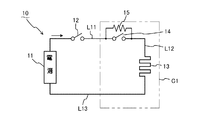
- FIG. 1 is a circuit diagram illustrating an electronic apparatus according to the first embodiment.
- the electronic device 10 includes a power supply 11, a first switch 12, a load 13, a second switch 14, and a resistor 15 which is an example of an electric element.
- the first switch 12 is, for example, a power switch, and is connected to at least the power supply and cuts off the power supplied from the power supply 11 to the load 13. In other words, the first switch 12 cuts off the power supplied from the power supply 11 to the control electric circuit C1 including the load 13, the second switch 14, and the resistor 15.
- the load 13 is an electric component such as a heater, for example.
- the second switch 14 is disposed closer to the load 13 than the first switch 12, for example, between the first switch 12 and the load 13, and cuts off power supplied from the power supply 11 to the load 13.
- Examples of the second switch 14 include an electric relay driven by an external control voltage, a controller such as a temperature switch that operates in response to a change in various physical quantities, and a manual operation switch. There is no particular limitation as long as the power supplied to the load 13 is interrupted.
- the first power line L11 is connected to one end of the second switch 14 on the first switch 12 side among the electrical contacts.
- the second power line L12 is connected to the other end of the electrical contacts of the second switch 14.
- the third power line L13 is connected to the load 13 and a pole opposite to the pole to which the first switch 12 of the power supply 11 is connected.
- the resistor 15 is connected between the first power line L11 and the second power line L12 in parallel with the electrical contact of the second switch 14.
- the resistor 15 is arranged, for example, outside the second switch 14, but may be connected inside the second switch 14 in parallel with the electrical contact of the second switch 14.
- the power consumption of the resistor 15 is, for example, less than 0.1 W.
- the resistance of the resistor 15 is, for example, 150 k ⁇ or more. Further, the resistance of the resistor 15 may be 1 M ⁇ or more. It is desirable that the heat generated in the resistor 15 be suppressed as much as possible.
- the condition under which the second switch 14 can operate most stably is a case where an appropriate voltage and current are controlled to open and close. In many cases, a clean surface appears on the surface of the contact, and even when the second switch 14 is closed, the contact is stabilized by the arc generated by the bounce of the electric contact.
- the first switch 12 cuts off the power and then the second switch 14 cuts off the power (that is, the electric contact of the second switch 14 is opened)
- the above-mentioned arc does not occur and the activation is not performed.
- Electrical contacts cannot be closed in this state. Therefore, even a small amount of foreign matter is likely to be affected.
- the surrounding static electricity is charged to a minimum portion (electric contact gap portion) of the separated conductive portion inside the electric circuit due to a phenomenon of electrostatic induction, so that the vicinity of the electric contact is generated. Insulating foreign matter, which is rarely present, is polarized by an electric field, and a Coulomb force acts on the foreign matter, causing the electric contact to be caught in a gap.
- the resistor 15 is connected to the second switch 14 so that the electrical contact of the second switch 14 is not charged.
- Fourteen electrical contacts are connected in parallel.
- the first switch 12 cuts off the power of the power supply 11
- the control electric circuit C1 disconnected from the power supply circuit having the power supply 11 and the first switch 12 has no voltage
- the second switch 14 is opened. Even in the state, foreign substances can be prevented from being introduced into the electrical contacts of the second switch 14.
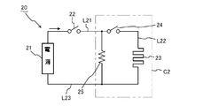
- FIG. 2 is a circuit diagram illustrating an electronic device 30 according to the second embodiment.
- the electronic device 20 includes a power supply 21, a first switch 22, a load 23, a second switch 24, and a resistor 25 which is an example of an electric element.
- the second embodiment is different from the first embodiment only in that the resistor 25 is connected between the first power line L21 and the third power line L23. Therefore, detailed description is omitted.
- FIG. 3 is a circuit diagram showing an electronic device 30 according to the third embodiment.
- the electronic device 30 includes a power supply 31, a first switch 32, a load 33, a second switch 34, a resistor 35 which is an example of an electric element, and a third switch 36.
- the third embodiment differs from the first embodiment only in that the first switch 32 and the third switch 36 disconnect both poles of the power supply 31. Therefore, detailed description is omitted.
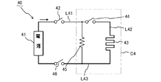
- FIG. 4 is a circuit diagram showing an electronic device 40 according to the fourth embodiment.
- the electronic device 40 includes a power supply 41, a first switch 42, a load 43, a second switch 44, a resistor 45 as an example of an electric element, and a third switch 46.
- the fourth embodiment differs from the second embodiment only in that the first switch 42 and the third switch 46 disconnect both poles of the power supply 41. Therefore, detailed description is omitted.
- the third power line L43 is connected to the third switch 46 and the load 43. That is, the third power line L43 is connected to a different pole of the power supply 41 from the pole to which the first switch 42 is connected.
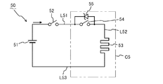
- FIG. 5 is a circuit diagram showing an electronic device 50 according to the fifth embodiment.
- the electronic device 50 includes a power supply 51, a first switch 52, a load 53, a second switch 54, and a constant voltage diode 55 which is an example of an electric element.
- control electric circuit C5 is different from the first embodiment only in that a constant voltage diode 55 is provided instead of the resistor 15 of the first embodiment shown in FIG. Therefore, detailed description is omitted.
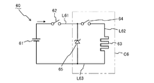
- FIG. 6 is a circuit diagram showing an electronic device 60 according to the sixth embodiment.
- the electronic device 60 includes a power supply 61, a first switch 62, a load 63, a second switch 64, and a constant voltage diode 65 which is an example of an electric element.
- the sixth embodiment differs from the above-described second embodiment only in that a constant voltage diode 65 is provided in the control electric circuit C6 instead of the resistor 25 of the second embodiment shown in FIG. Therefore, detailed description is omitted.
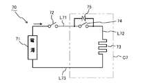
- FIG. 7 is a circuit diagram showing an electronic device 70 according to the seventh embodiment.
- the electronic device 70 includes a power supply 71, a first switch 72, a load 73, a second switch 74, and a lightning arrester 75 which is an example of an electric element.
- the seventh embodiment differs from the first embodiment only in that a lightning arrester 75 is arranged in the control electric circuit C7 instead of the resistor 15 of the first embodiment shown in FIG. Therefore, detailed description is omitted.
- the lightning arrester 75 is, for example, a varistor applicable to the voltage of the power supply 71.
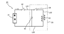
- FIG. 8 is a circuit diagram showing an electronic device 80 according to the eighth embodiment. As shown in FIG. 8, the electronic device 80 includes a power supply 81, a first switch 82, a load 83, a second switch 84, and a lightning arrester 85 as an example of an electric element.
- the eighth embodiment is different from the above-mentioned second embodiment only in that a lightning arrester 85 is arranged in the control electric circuit C8 instead of the resistor 25 of the second embodiment shown in FIG. Therefore, detailed description is omitted.
- the lightning arrester 85 is, for example, a varistor applicable to the voltage of the power supply 81.
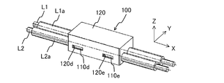
- FIG. 9 is a perspective view showing case 100 in the embodiment together with first power line L1 and second power line L2.
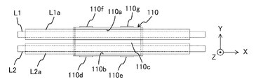
- FIG. 10 is a plan view showing first case member 110 according to the embodiment together with first power line L1 and second power line L2.
- FIG. 11 is a right side view showing the first case member 110 according to the embodiment.
- FIG. 12 is a bottom view showing the second case member 120 according to the embodiment together with the electric element 500.
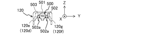
- FIG. 13 is a right side view showing an internal structure of second case member 120 together with electric element 500 in the embodiment.
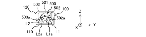
- FIG. 14 is a right side view showing the internal structure of the case 100 according to the embodiment together with the first power line L1, the second power line L2, and the electric element 500.
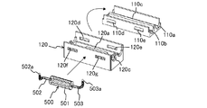
- FIG. 15 is an exploded perspective view showing the case 100 and the electric element 500 according to the embodiment.
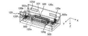
- FIG. 16 is a perspective view showing an internal structure of second case member 120 in the embodiment together with electric element 500.
- FIG. 17 is an exploded perspective view showing the case 100 and the electric element 500 together with the first power line L1 and the second power line L2 in the embodiment.
- the X, Y, and Z directions shown in FIGS. 9 to 14 and 16 are given as examples for convenience of description.
- the X, Y, and Z directions are orthogonal to each other.
- the first power line L1 (the above-described first power lines L11, L21, L31, L41, L51, L61, L71, L81) and the second power line L2 (the above-described second power lines L12, L22, L32) are used.
- L42, L52, L62, L72, L82 in FIG. 9 and FIG.
- the Y direction is the arrangement direction of the first power line L1 and the second power line L2.
- the Z direction is a direction in which the first case member 110 and the second case member 120 of the case 100 are fitted.
- the second power line L2 will be described as an example. ) May be arranged.
- the case 100 has a first case member 110 and a second case member 120 that are fitted together.
- the case 100 is made of, for example, an insulating synthetic resin.
- Each of the first case member 110 and the second case member 120 has a shape close to a rectangular parallelepiped shape in which each side is parallel in the X direction, the Y direction, or the Z direction, and the first case member 110 is in the front in the Z direction.
- the second case member 120 opens rearward in the Z direction.
- the first power line L1 is connected to the first switch at the electrical contact of the second switch 14, 24, 34, 44, 54, 64, 74, 84 described above. 12, 22, 32, 42, 52, 62, 72, and 82 are connected to one end. At least a region of the first power line L1 where the case 100 is arranged is provided with an insulating covering portion L1a on the outer periphery.
- the second power line L2 is connected to the other end of the electrical contact of the second switch 14, 24, 34, 44, 54, 64, 74, 84 (that is, the first switch 12, 22, 32). , 42, 52, 62, 72, 82). At least a region of the second power line L2 where the case 100 is arranged is provided with an insulating covering portion L2a on the outer periphery.
- the electric element 500 shown in FIGS. 12 to 17 is, for example, the above-described resistors 15, 25, 35, 45, constant voltage diodes 55, 65, lightning arresters 75, 85, and the like.
- the electric element 500 protrudes from the electric element main body 501, the electric element main body 501, and is connected to the first power line L1, and protrudes from the electric element main body 501, and is connected to the second power line L2. And a second terminal 503.
- the electric element 500 is housed in the case 100.
- the first terminal 502 protrudes rearward in the X direction from the electric element body 501, for example, and then bends vertically forward in the Y direction, and then vertically bends rearward in the Z direction.
- the first terminal 502 has a first tapered portion 502a at a tip opposite to the electric element body 501, that is, at a portion extending rearward in the Z direction.
- the second terminal 503 protrudes forward from the electric element body 501 in the X direction, then bends vertically backward in the Y direction, and then bends vertically backward in the Z direction.
- the second terminal 503 has a second tapered portion 503a at a tip opposite to the electric element body 501, that is, at a portion extending rearward in the Z direction.
- the first case member 110 includes a first power line holding unit 110 a that holds the first power line L ⁇ b> 1 covering portion L ⁇ b> 1, and a second power line L ⁇ b> 2 covering the first power line L ⁇ b> 2. And a second power line holding unit 110b that holds the unit L2a.
- the first case member 110 has, for example, a flat plate-shaped partition wall 110c protruding forward in the Z direction so as to partition the first power line L1 and the second power line L2.
- the first power line holding unit 110a is a concave portion having a semicircular cross section so as to cover, for example, half of the outer periphery of the first power line L1.
- the second power line holding unit 110b is a concave portion having a semicircular cross section so as to cover, for example, half of the outer periphery of the second power line L2. These recesses may be provided only on the surfaces at both ends in the X direction of the first case member 110.
- locking claws 110d and 110e projecting rearward in the Y direction are provided on the rear surface of the first case member 110 in the Y direction.
- Locking claws 110f and 110g projecting forward in the Y direction are provided on the front surface of the first case member 110 in the Y direction.
- the second case member 120 includes an electric element main body holding unit 120 a that holds the electric element main body 501, and a first terminal holding unit that holds the first terminal 502. It has a portion 120b and a second terminal holding portion 120c that holds the second terminal 503.
- the electric element main body holding section 120a is, for example, a pair of flat plate-like parts that are arranged with the electric element main body 501 interposed therebetween and protrude rearward in the Z direction.
- the first terminal holding portion 120b is a portion that projects rearward in the Z direction so as to sandwich at least a part of the first terminal 502, for example.
- the second terminal holding portion 120c is a portion that projects rearward in the Z direction so as to sandwich at least a part of the second terminal 503, for example.
- the second case member 120 has, like the first case member 110, a half of the outer periphery of the first power line L ⁇ b> 1 or the second power line L ⁇ b> 2 on both surfaces in the X direction. Is provided so as to cover the recess.
- locking holes 120 d and 120 e into which locking claws 110 d and 110 e are inserted are provided on the rear surface in the Y direction of the second case member 120. .
- Locking holes 120f and 120g into which the locking claws 110f and 110g are inserted are provided on the front surface of the second case member 120 in the Y direction. The first case member 110 and the second case member 120 are locked by inserting the locking claws 110d, 110e, 110f, 110g into the locking holes 120d, 120e, 120f, 120g.
- the electric element 500 is held by the second case member 120,
- the case member 110 holds the first power line L1 and the second power line L2.
- the first case member 110 and the second case member 120 are fitted to each other, so that the first tapered portion 502a of the first terminal 502 penetrates the covering portion L1a of the first power line L1,
- the second tapered portion 503a of the second terminal 503 penetrates the covering portion L2a of the second power line L2.
- the electric element 500 is connected to the first power line L1 at the first terminal 502 and connected to the second power line L2 at the second terminal 503.
- the first tapered portion 502a of the first terminal 502 of the electric element 500 and the first power line L1 and the second tapered portion 503a of the second terminal 503 and the second power line L2 (or the third power line) to easily connect the electric element 500 to the first power line.
- An electrical contact of the second switch 14, 24, 34, 44, 54, 64, 74, 84 can be connected in parallel between L1 and the second power line L2 (or between the first power line L1 and the second power line L2). 3 power line).
- first case member 100 has a first power line holding portion 110a and a second power line holding portion 110b
- second case member 120 has an electric element main body holding portion 120a, a first terminal holding portion 120b
- the second terminal holding portion 120c allows the electric element 500 to be easily and reliably connected in parallel to the electric contacts of the second switches 14, 24, 34, 44, 54, 64, 74, 84. Can be.
- An electronic device comprising: an electric element connected in parallel to an electric contact or connected between the first power line and the third power line.
- the electric element is a resistor, The electronic device according to claim 1, wherein the resistor has a power consumption of less than 0.1 W.
- the first case member includes a first power line holding portion that holds the covering portion of the first power line, and a second power line that holds the covering portion of the second power line or the third power line. Holding part,
- the second case member includes an electric element main body holding portion that holds the electric element main body, a first terminal holding portion that holds the first terminal, and a second terminal that holds the second terminal.
Landscapes
- Engineering & Computer Science (AREA)
- Physics & Mathematics (AREA)
- Electromagnetism (AREA)
- General Physics & Mathematics (AREA)
- Radar, Positioning & Navigation (AREA)
- Automation & Control Theory (AREA)
- Microelectronics & Electronic Packaging (AREA)
- Emergency Protection Circuit Devices (AREA)
- Keying Circuit Devices (AREA)
- Direct Current Feeding And Distribution (AREA)
Abstract
L'invention concerne un appareil électronique (10) comprenant : une source d'alimentation (11) ; un premier commutateur (12) qui est connecté au moins à l'une des électrodes de la source d'alimentation (11) et qui bloque la puissance fournie par la source d'alimentation (11) à une charge (13) ; un second commutateur (14) qui est disposé sur le coté de charge (13) du premier commutateur (12) et qui bloque la puissance fournie par la source d'alimentation (11) à la charge (13) ; une première ligne d'alimentation (L11) qui est connectée à, des contacts électriques du second commutateur (14), une borne qui se trouve sur le côté du premier commutateur (12) ; une deuxième ligne d'alimentation (L12) qui est connectée à l'autre borne des contacts électriques du second commutateur (14) ; une troisième ligne d'alimentation (L13) qui est connectée à l'autre électrode de la source d'alimentation (11) ; et un élément électrique (résistance 15) qui est connecté, en parallèle avec les contacts électriques, entre la première ligne d'alimentation (L11) et la deuxième ligne d'alimentation (L12) ou entre la première ligne d'alimentation (L11) et la troisième ligne d'alimentation (L13) de manière à empêcher les contacts électriques du second commutateur (14) d'être chargés, dans l'état où la puissance est bloquée par le premier commutateur (12) et le second commutateur (14).
Priority Applications (4)
| Application Number | Priority Date | Filing Date | Title |
|---|---|---|---|
| DE112019003244.5T DE112019003244T5 (de) | 2018-06-27 | 2019-02-21 | Elektrisches gerät |
| JP2020527188A JP7311163B2 (ja) | 2018-06-27 | 2019-02-21 | 電子機器 |
| US17/250,176 US11532442B2 (en) | 2018-06-27 | 2019-02-21 | Electronic device with case having sheath-piercing tapered sections |
| CN201980040788.XA CN112292744B (zh) | 2018-06-27 | 2019-02-21 | 电子设备 |
Applications Claiming Priority (2)
| Application Number | Priority Date | Filing Date | Title |
|---|---|---|---|
| JP2018-122227 | 2018-06-27 | ||
| JP2018122227 | 2018-06-27 |
Publications (1)
| Publication Number | Publication Date |
|---|---|
| WO2020003596A1 true WO2020003596A1 (fr) | 2020-01-02 |
Family
ID=68986281
Family Applications (1)
| Application Number | Title | Priority Date | Filing Date |
|---|---|---|---|
| PCT/JP2019/006460 Ceased WO2020003596A1 (fr) | 2018-06-27 | 2019-02-21 | Appareil électronique |
Country Status (5)
| Country | Link |
|---|---|
| US (1) | US11532442B2 (fr) |
| JP (1) | JP7311163B2 (fr) |
| CN (1) | CN112292744B (fr) |
| DE (1) | DE112019003244T5 (fr) |
| WO (1) | WO2020003596A1 (fr) |
Families Citing this family (1)
| Publication number | Priority date | Publication date | Assignee | Title |
|---|---|---|---|---|
| US20250046547A1 (en) * | 2021-12-27 | 2025-02-06 | Mitsubishi Electric Corporation | Switching device |
Citations (4)
| Publication number | Priority date | Publication date | Assignee | Title |
|---|---|---|---|---|
| JP2004103383A (ja) * | 2002-09-09 | 2004-04-02 | Unimekkusu Kk | 電源コードに着脱自在な導通コネクター |
| JP2008071514A (ja) * | 2006-09-12 | 2008-03-27 | Auto Network Gijutsu Kenkyusho:Kk | コネクタ |
| JP2014216056A (ja) * | 2013-04-22 | 2014-11-17 | 富士電機株式会社 | 直流回路遮断装置 |
| JP2016062790A (ja) * | 2014-09-19 | 2016-04-25 | 富士電機株式会社 | ハイブリッド形開閉器 |
Family Cites Families (36)
| Publication number | Priority date | Publication date | Assignee | Title |
|---|---|---|---|---|
| JP2868354B2 (ja) | 1992-02-25 | 1999-03-10 | 東北日本電気株式会社 | 導通試験装置 |
| JPH10247433A (ja) | 1997-03-03 | 1998-09-14 | Tempearl Ind Co Ltd | 接点を有する開閉器等の構造 |
| JP3825583B2 (ja) * | 1999-06-25 | 2006-09-27 | ウチヤ・サーモスタット株式会社 | 感熱遮断装置および電池パック |
| JP4672219B2 (ja) * | 2001-09-11 | 2011-04-20 | ウチヤ・サーモスタット株式会社 | 安全装置 |
| KR100434153B1 (ko) * | 2002-04-12 | 2004-06-04 | 엘지산전 주식회사 | 하이브리드 직류 전자 접촉기 |
| JP2004014434A (ja) * | 2002-06-11 | 2004-01-15 | Uchiya Thermostat Kk | 直流電流遮断スイッチ |
| JP4050098B2 (ja) * | 2002-06-11 | 2008-02-20 | ウチヤ・サーモスタット株式会社 | 直流電流遮断スイッチ |
| JP2004103388A (ja) * | 2002-09-10 | 2004-04-02 | Sanyo Electric Co Ltd | マグネトロン |
| CN2681373Y (zh) * | 2003-10-27 | 2005-02-23 | 陈静雄 | 穿刺式电线连接器 |
| JP5076415B2 (ja) | 2006-09-14 | 2012-11-21 | 日本精工株式会社 | 電動パワーステアリング制御装置 |
| DE102006049563B3 (de) * | 2006-10-20 | 2008-04-17 | Tyco Electronics Amp Gmbh | Steckverbinder mit verbesserter Kabelzugentlastung |
| JP2009117150A (ja) | 2007-11-06 | 2009-05-28 | Fuji Electric Fa Components & Systems Co Ltd | 回路遮断器の接点構造 |
| CN102341878B (zh) * | 2009-03-12 | 2014-02-12 | 打矢恒温器株式会社 | 热控开关 |
| CN201435453Y (zh) * | 2009-06-17 | 2010-03-31 | 王嘉鑫 | 电连接器 |
| WO2011034140A1 (fr) * | 2009-09-16 | 2011-03-24 | 株式会社ワイ・ワイ・エル | Commutateur |
| CN102598183B (zh) * | 2009-11-04 | 2014-07-23 | 打矢恒温器株式会社 | 连接了带三端子的热控开关的电路及其连接方法 |
| CN103597566B (zh) * | 2011-07-04 | 2016-03-30 | 打矢恒温器株式会社 | 温度开关 |
| US20150022928A1 (en) * | 2011-12-22 | 2015-01-22 | Siemens Aktiengesellschaft | Hybrid dc circuit breaking device |
| CN202454733U (zh) * | 2012-01-20 | 2012-09-26 | 江门市创艺电器有限公司 | 一种快速接线端子 |
| CN202695753U (zh) * | 2012-05-21 | 2013-01-23 | 北汽福田汽车股份有限公司 | 接线端子 |
| JP6110408B2 (ja) * | 2012-11-30 | 2017-04-05 | ウチヤ・サーモスタット株式会社 | 温度センサ |
| JP6143615B2 (ja) * | 2013-09-03 | 2017-06-07 | 富士電機株式会社 | 直流開閉器 |
| CN103560023B (zh) * | 2013-11-15 | 2015-10-14 | 沈阳工业大学 | 一种三断口双动式高速永磁斥力开关及方法 |
| JP6284827B2 (ja) * | 2014-05-29 | 2018-02-28 | 富士電機株式会社 | 開閉器 |
| DE102014008706A1 (de) * | 2014-06-18 | 2015-12-24 | Ellenberger & Poensgen Gmbh | Trennschalter zur Gleichstromunterbrechung |
| CN204424194U (zh) * | 2015-02-06 | 2015-06-24 | 孙毅彪 | 无电弧型桥式高压电力断路器 |
| CN204497130U (zh) * | 2015-03-14 | 2015-07-22 | 孙毅彪 | 增压臂式无电弧型高压电力断路器 |
| DE102015212802A1 (de) * | 2015-07-08 | 2017-01-12 | Ellenberger & Poensgen Gmbh | Trennvorrichtung zur Gleichstromunterbrechung |
| FR3043833B1 (fr) * | 2015-11-17 | 2017-12-22 | Inst Supergrid | Disjoncteur pour un reseau a courant continu haute tension, avec oscillation forcee de courant |
| WO2017130518A1 (fr) * | 2016-01-26 | 2017-08-03 | ウチヤ・サーモスタット株式会社 | Thermocontact et boîtier isolant pour thermocontact |
| JP2018006209A (ja) | 2016-07-05 | 2018-01-11 | 富士通コンポーネント株式会社 | 電磁継電器 |
| CN206628604U (zh) * | 2017-03-08 | 2017-11-10 | 台达电子工业股份有限公司 | 适用于电源转接器的电缆连接器组件 |
| DE112017007449T5 (de) * | 2017-04-18 | 2020-01-23 | Uchiya Thermostat Co., Ltd. | Temperaturausgelöster Schalter |
| JP7200528B2 (ja) * | 2017-12-20 | 2023-01-10 | 富士電機株式会社 | 電流遮断器 |
| CN112805799B (zh) * | 2018-10-18 | 2025-03-07 | 打矢恒温器株式会社 | 电气元件的连接方法 |
| JP7513872B2 (ja) * | 2020-04-28 | 2024-07-10 | 日亜化学工業株式会社 | レーザ光源の製造方法 |
-
2019
- 2019-02-21 WO PCT/JP2019/006460 patent/WO2020003596A1/fr not_active Ceased
- 2019-02-21 DE DE112019003244.5T patent/DE112019003244T5/de not_active Ceased
- 2019-02-21 CN CN201980040788.XA patent/CN112292744B/zh active Active
- 2019-02-21 US US17/250,176 patent/US11532442B2/en active Active
- 2019-02-21 JP JP2020527188A patent/JP7311163B2/ja active Active
Patent Citations (4)
| Publication number | Priority date | Publication date | Assignee | Title |
|---|---|---|---|---|
| JP2004103383A (ja) * | 2002-09-09 | 2004-04-02 | Unimekkusu Kk | 電源コードに着脱自在な導通コネクター |
| JP2008071514A (ja) * | 2006-09-12 | 2008-03-27 | Auto Network Gijutsu Kenkyusho:Kk | コネクタ |
| JP2014216056A (ja) * | 2013-04-22 | 2014-11-17 | 富士電機株式会社 | 直流回路遮断装置 |
| JP2016062790A (ja) * | 2014-09-19 | 2016-04-25 | 富士電機株式会社 | ハイブリッド形開閉器 |
Also Published As
| Publication number | Publication date |
|---|---|
| DE112019003244T5 (de) | 2021-05-06 |
| US20210159026A1 (en) | 2021-05-27 |
| CN112292744B (zh) | 2024-03-19 |
| US11532442B2 (en) | 2022-12-20 |
| CN112292744A (zh) | 2021-01-29 |
| JP7311163B2 (ja) | 2023-07-19 |
| JPWO2020003596A1 (ja) | 2021-07-15 |
Similar Documents
| Publication | Publication Date | Title |
|---|---|---|
| JP6998848B2 (ja) | 直流アーク検出/抑制のための方法及び装置 | |
| US7161785B2 (en) | Apparatus for high surge voltage protection | |
| US7969275B2 (en) | Fuse assembly with integrated current sensing | |
| US4876621A (en) | Line protector for a communications circuit | |
| US4322777A (en) | Circuit board formed with spark gap | |
| CN205140660U (zh) | 过压保护元件 | |
| WO2009051385A2 (fr) | Fusible thermique pourvu d'une fonction de fusible de protection contre les surintensités | |
| RU2009110964A (ru) | Разрядник защиты от перенапряжения, содержащий корпус и, по меньшей мере, один разрядный элемент | |
| CN104882342B (zh) | 复合保护装置 | |
| US20140334050A1 (en) | Passive arc suppressor | |
| JP7311163B2 (ja) | 電子機器 | |
| US20050041349A1 (en) | Overvoltage protection device | |
| EP3384509B1 (fr) | Varistances | |
| KR930011387B1 (ko) | 안전보장기능을 가진 전자부품 | |
| US4237515A (en) | Protective electrical discharge device | |
| US20200144012A1 (en) | Surge protection device with connection elements and method for producing same | |
| CN105914726B (zh) | 安装在印刷电路板上的过电压保护器装置 | |
| RU2680961C2 (ru) | Вставной элемент для устройства защиты электрооборудования и устройство защиты электрооборудования с таким вставным элементом | |
| EP2482295B1 (fr) | Relais avec plusieurs contacts | |
| JP2019003844A (ja) | 高周波分離ヒューズ | |
| US5436787A (en) | Surge arrestor unit | |
| JP2002319746A (ja) | 雷サージ電圧回避装置 | |
| JPH1050453A (ja) | 回路保護装置及びプリント基板 | |
| JP2008199862A (ja) | フィルタ付電源用保安器 | |
| KR20200021228A (ko) | 송전 선로의 누설 전류 제한장치 |
Legal Events
| Date | Code | Title | Description |
|---|---|---|---|
| 121 | Ep: the epo has been informed by wipo that ep was designated in this application |
Ref document number: 19827342 Country of ref document: EP Kind code of ref document: A1 |
|
| ENP | Entry into the national phase |
Ref document number: 2020527188 Country of ref document: JP Kind code of ref document: A |
|
| 122 | Ep: pct application non-entry in european phase |
Ref document number: 19827342 Country of ref document: EP Kind code of ref document: A1 |