WO2020003689A1 - Matériau phononique et son procédé de production - Google Patents
Matériau phononique et son procédé de production Download PDFInfo
- Publication number
- WO2020003689A1 WO2020003689A1 PCT/JP2019/015278 JP2019015278W WO2020003689A1 WO 2020003689 A1 WO2020003689 A1 WO 2020003689A1 JP 2019015278 W JP2019015278 W JP 2019015278W WO 2020003689 A1 WO2020003689 A1 WO 2020003689A1
- Authority
- WO
- WIPO (PCT)
- Prior art keywords
- temperature
- phononic
- periodic structure
- cooling
- material according
- Prior art date
- Legal status (The legal status is an assumption and is not a legal conclusion. Google has not performed a legal analysis and makes no representation as to the accuracy of the status listed.)
- Ceased
Links
Images







Classifications
-
- H—ELECTRICITY
- H01—ELECTRIC ELEMENTS
- H01F—MAGNETS; INDUCTANCES; TRANSFORMERS; SELECTION OF MATERIALS FOR THEIR MAGNETIC PROPERTIES
- H01F1/00—Magnets or magnetic bodies characterised by the magnetic materials therefor; Selection of materials for their magnetic properties
-
- H—ELECTRICITY
- H01—ELECTRIC ELEMENTS
- H01B—CABLES; CONDUCTORS; INSULATORS; SELECTION OF MATERIALS FOR THEIR CONDUCTIVE, INSULATING OR DIELECTRIC PROPERTIES
- H01B12/00—Superconductive or hyperconductive conductors, cables, or transmission lines
Definitions
- the present invention relates to a phononic material exhibiting physical properties different from those inherent to a constituent substance and a method for producing the same.
- Non-Patent Document 1 Research on phonon engineering for artificially manipulating phonons propagating in the constituent material by periodically arranging arbitrary structures in the material has been advanced.
- the present inventor has succeeded in applying phonon engineering to an insulator to reduce the thermal conductivity of the insulator by about one digit (see Non-Patent Document 1).
- the propagation of heat in the material is explained by the propagation of phonons (lattice vibrations).
- the phonon dispersion relation is determined by the type of the substance, and the thermal conductivity is determined by the phonon dispersion relation originally possessed by the substance.
- the phonon dispersion relation is determined. By artificially manipulating, the thermal conductivity inherently possessed by the insulator can be reduced.
- an object of the present invention is to provide a phononic material in which at least one of the physical properties of the magnetic properties and the electrical conductivity of the constituent material is changed from a property unique to the constituent material, and a method of manufacturing the same.
- the present inventor has found that when a periodic structure in which a structure is periodically arranged in a constituent material is cooled, the constituent material is present before cooling.
- the material order that has been changed changes to form a new material order, and this new material order is maintained even after the temperature rises, and the physical properties differ from the intrinsic magnetic and electrical conductivity of the constituent materials.
- This phenomenon is not confirmed even when the constituent material is simply cooled, it occurs only in the constituent material constituting the periodic structure, and phonons (lattice vibrations) in the constituent material constituting the periodic structure are not included.
- the new material order to be formed differs depending on what kind of the material order is experienced by the periodic structure during the cooling process. This means that, through the control of phonons based on artificial setting of the structure arranged in the periodic structure, the material order that the constituent material originally cannot have can be artificially expressed. .
- the present invention is based on the above findings, and means for solving the above problems are as follows. That is, ⁇ 1>
- the structure has a periodic structure in which a structure is periodically arranged in a constituent material, and the physical structure of at least one of the magnetic structure and the electrical conductivity of the periodic structure is compared at room temperature.
- a phononic material characterized by being different from a material specific to a substance.
- ⁇ 3> The phononic material according to any one of ⁇ 1> to ⁇ 2>, wherein the periodic structure is formed in a layer shape, and the structure is a through hole.
- ⁇ 4> The phononic material according to any one of ⁇ 1> to ⁇ 3>, wherein the periodic structure has any one of a resistance minimum and a resistance maximum under a temperature condition of 250 K or less.
- ⁇ 5> The phononic material according to any one of ⁇ 1> to ⁇ 4>, wherein the magnetic susceptibility of the periodic structure at room temperature is ⁇ 1 ⁇ 10 ⁇ 3 or less.
- ⁇ 6> The method for producing a phononic material according to any one of ⁇ 1> to ⁇ 5>, wherein the cooling step includes cooling the periodic structure at a cooling rate of 10 K / min or less to a cooling temperature of 250 K or less; A temperature raising step of raising the temperature of the periodic structure to a temperature higher than the cooling temperature after the cooling step.
- ⁇ 7> The method for producing a phononic material according to ⁇ 6>, wherein the cooling step and the temperature raising step are alternately and repeatedly performed.
- ⁇ 8> The method for producing a phononic material according to any one of ⁇ 6> to ⁇ 7>, wherein the cooling step is performed at a cooling temperature within a temperature range in which physical properties required of the phononic material are exhibited.
- FIG. 2 is an explanatory diagram showing a cross section taken along line A-A ′ in FIG. It is a figure (1) which shows the modification of a structure.
- FIG. 9 is a diagram (2) illustrating a modification of the structure.
- FIG. 9 is a diagram (3) illustrating a modification of the structure.
- It is a figure (4) which shows the modification of a structure.
- It is explanatory drawing which shows the structural example of a one-dimensional phononic material.
- It is explanatory drawing (1) which shows the structural example of a three-dimensional phononic material.
- It is explanatory drawing (2) which shows the structural example of a three-dimensional phononic material.
- FIG. 3 is an explanatory diagram showing a state when the niobium layer in Example 1 is viewed from above. It is explanatory drawing which shows the rectangular block area
- FIG. 4 is a diagram showing the state of execution of the cooling step and the temperature raising step in the phononic material according to the first embodiment.
- FIG. 7 is a diagram showing the external magnetic field dependence of magnetization at room temperature (300 K) of the phononic material according to Example 2.
- FIG. 13 is an explanatory diagram showing a state when the niobium layer in Example 3 is viewed from above.
- FIG. 9 is a view showing the state of execution of the cooling step and the temperature raising step in the phononic material according to Example 3.
- the phononic material of the present invention has a periodic structure, and the physical properties of at least one of the magnetic property and the electrical conductivity of the constituent material in the periodic structure are different from those specific to the constituent material when compared at room temperature. It is characterized by.
- the periodic structure is configured by periodically arranging structures in the constituent material.
- the periodic structure having such a configuration is also called a phononic crystal in comparison with a normal crystal showing a state in which atoms and molecules are periodically arranged in a substance.
- the arrangement of the structures can be set artificially, and the setting method is of interest as phonon engineering.
- a property in which the group velocity and the energy density of phonons are smaller than that of the constituent material in a bulk state having no structure appears.
- This property varies in degree depending on how the structures are arranged. That is, in the periodic structure, the phonon group velocity and the energy density can be changed by the applied phonon engineering.
- the group velocity and the energy density of these phonons are such that as one becomes smaller, the other becomes smaller, and as one becomes larger, the other becomes larger.
- the periodic structure is not particularly limited, but the smaller the group velocity and the energy density of phonons, the easier it is to control the behavior of electrons in the constituent material. It is preferable that the group velocity of phonon in the constituent material in the periodic structure is not more than ⁇ ⁇ as compared with the constituent material in the bulk state, when focusing on the group velocity.
- the constituent material is not particularly limited and can be appropriately selected depending on the purpose. That is, in the phononic material, the phonon in the constituent material acquires a property different from the physical property unique to the constituent material by utilizing a phenomenon in which the phonon interacts with an electron in the constituent material at the time of cooling. It can happen with substances. This is because phonons always exist as long as they are substances. Above all, as the constituent material, a substance containing a transition metal (element belonging to Group 3 to Group 12) is preferable, and a substance composed of a single substance of the transition metal element is particularly preferable. That is, since the transition metal has d electrons, it is easy to cause an interaction with phonon, and further, it is easy to construct a new material order utilizing these interactions.
- a transition metal element belonging to Group 3 to Group 12
- the structure is not particularly limited and can be selected according to the purpose.
- Examples of the structure include known structures applied to the phononic crystal.
- the structure when the periodic structure is formed in a layer, it is preferable that the structure be a through hole formed in the thickness direction of the layer.
- the periodic structure can be manufactured by a known lithography process, and a group of the structures regularly arranged in the periodic structure can be easily obtained.
- the through-hole When the structure is formed as the through-hole, the through-hole may be filled with a filling material formed of a material different from the constituent material to adjust the group velocity and energy density of phonons.
- the structure formed of a plurality of structures having different shapes is referred to as a unit structure. This includes the case where the structure is repeatedly arranged.
- the period at which the structure is formed on the periodic structure is a phonon wavelength scale (for example, a scale of nanometer order to millimeter order (10 nm to 10 mm)).
- a phonon wavelength scale for example, a scale of nanometer order to millimeter order (10 nm to 10 mm)
- the size of the structure may be a phonon wavelength scale (for example, a scale of nanometer order to millimeter order (10 nm to 10 mm)).
- the group velocity and energy density of phonons in the constituent material are smaller than those of the constituent material in the bulk state.
- the size of the structure corresponds to the maximum diameter of the structure, for example, in the through hole, if the opening diameter is larger than the depth, the opening diameter corresponds, When the opening diameter has a shape whose length is larger than its width, the length corresponds to the length.
- the periodic structure is not particularly limited, and may be manufactured according to a known phononic crystal manufacturing method, or a previously manufactured known phononic crystal may be obtained and used.
- the physical properties of the phononic material vary depending on the order experienced by the periodic structure during the cooling process, and the electrical resistance of the periodic structure has a minimum resistance and a maximum resistance under a temperature condition of 250 K or less. It is preferable to have any of the following characteristics. When such physical properties are developed, it becomes easy to localize the electrons of the constituent material in the periodic structure, and at least one of the physical properties of magnetism and electric conductivity is different from the phononic material unique to the constituent material. Can be realized.
- the magnetic susceptibility of the periodic structure be -1 ⁇ 10 ⁇ 3 or less at room temperature and exhibit diamagnetism.
- the diamagnetic material can be constituted by the new constituent material, and the scope of choice of the constituent material of the diamagnetic material and application examples of the diamagnetic material in the real world can be expanded.
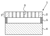
- FIG. 1A is an explanatory diagram showing an upper surface of a phononic material according to an embodiment of the present invention
- FIG. 1B is an explanatory diagram showing a cross section taken along line AA ′ in FIG. It is.
- the phononic material 1 has a periodic structure 2 ′ in which cylindrical through-holes are regularly arranged as a structural body 3 in a constituent substance 2.
- the periodic structure 2 ′ is disposed on the substrate 4 via the spacer 5.
- the spacer 5 is arranged so as to support the periodic structure 2 ′ at an outer peripheral position of a region where the structure 3 is formed.
- the substrate 4 and the spacer 5 are provided in order to measure a change in physical properties of the periodic structure 2 ′ at the time of cooling, and a region on the bottom surface (surface on the substrate 4 side) side of the periodic structure 2 ′ on which the structure 3 is formed.
- the substrate 4 is made of a material having a small magnetic susceptibility such as Si
- the spacer 5 is made of a material having a small magnetic susceptibility such as SiO 2 and an electrically insulating material. Be composed. Note that the substrate 4 and the spacer 5 may be removed before and after the desired physical properties are exhibited in the periodic structure 2 ′, and the periodic structure 2 ′ itself may be made of a phononic material.
- FIGS. 1A and 1B The periodic structure 2 ′ shown in FIGS. 1A and 1B is an example for explanation, and the structure, number of formation, arrangement, and the like of the structure 3 are appropriately set according to the purpose. You can choose. Modifications of the structure 3 are shown in FIGS. FIGS. 2A to 2D are diagrams (1) to (4) showing modified examples of the structure.
- the structure is formed as a substantially square pillar-shaped through hole.
- the regularity of arranging the through holes shown in FIG. 2A is changed.
- the phononic crystal may have a property that the group velocity and the energy density of phonons are lower than those of the constituent material in the bulk state.
- 2 (c) and 2 (d) show an example in which the structure composed of a plurality of structures having different shapes is defined as a unit structure, and the unit structure is repeatedly arranged to configure the periodic structure. Is shown. Also in the periodic structure in which the unit structure is formed as the structure, the phononic crystal may have a property that the group velocity and the energy density of phonons are smaller than those of the constituent material in the bulk state.
- FIG. 3A is an explanatory diagram illustrating a configuration example of a one-dimensional phononic material
- FIG. 3B is an explanatory diagram (1) illustrating a configuration example of a three-dimensional phononic material
- FIG. 3C is an explanatory view (2) showing a configuration example of a three-dimensional phononic material.
- the arrangement of the structures 13 is a one-dimensional arrangement having periodicity in the length direction of the periodic structure 12.
- a layer of the constituent substance 22a on which the structure 23a is formed which is formed in the same manner as the periodic structure 2 ′ shown in FIGS. 1A and 1B.
- the arrangement of the structures 23a and b is added to the width direction and the length direction of the periodic structure 22, The arrangement is three-dimensional with periodicity in the directions.
- symbol 24 in FIG.3 (b) shows a board
- symbol 25 shows a spacer.
- the cubic block region 26 in which a circular hole as the structure 23 ′ is formed on each surface as a unit structure, and the unit structure is the periodic structure 22 ′. are configured to have a three-dimensional periodic array in which a plurality of combinations are made in the height direction, the width direction, and the length direction.
- the periodic structure 22 ' can be manufactured by a known 3D printer or the like.
- the constituent material in the periodic structure is given different physical properties from the constituent material in the bulk state by implementing the phononic material manufacturing method described below.
- the method for producing a phononic material of the present invention includes a cooling step and a temperature increasing step, and further includes other steps as necessary.
- This manufacturing method is a method for manufacturing the phononic material of the present invention, and the same items as those described for the phononic material are applied to the periodic structure used in the present manufacturing method.
- the cooling step is a step of cooling the periodic structure at a cooling rate of 10 K / min or less to a cooling temperature of 250 K or less.
- the reason why the cooling rate is set to 10 K / min or less is that, when the cooling rate exceeds 10 K / min, the change in the material order is caused by the temperature change rather than the change in the material order due to the progress of the interaction between phonons and electrons in the constituent material. This is because normal substance change becomes dominant, and it is difficult to obtain a new material order.
- the reason why the cooling temperature is set to 250 K or less is that the formation of the new material order is confirmed from around 250 K.
- As a specific method of setting the cooling temperature There is a method of setting a temperature at which a substance shows physical properties different from those of the constituent substance in the bulk state. In the phononic material, different physical properties may be exhibited depending on the cooling temperature. Therefore, it is preferable that the cooling step is performed at a cooling temperature within a temperature range in which physical properties required for the phononic material are exhibited.
- the cooling step is not particularly limited, but is preferably performed in any of a vacuum atmosphere of 1 ⁇ 10 ⁇ 3 Pa or less and a helium gas atmosphere of about 100 Pa to 100 kPa.
- a vacuum atmosphere 1 ⁇ 10 ⁇ 3 Pa or less
- a helium gas atmosphere of about 100 Pa to 100 kPa.
- the periodic structure can be easily cooled to a target temperature.
- a device for performing the cooling step and a known refrigerant dewar or refrigerator can be used.
- the temperature raising step is a step of, after the cooling step, raising the temperature of the periodic structure to a temperature higher than the cooling temperature.
- the order experienced in the cooling step is maintained even when the temperature is raised to a temperature exceeding the cooling temperature.
- the heating rate in the heating step is not particularly limited and can be appropriately selected according to the purpose.
- the apparatus for performing the temperature raising step and the apparatus used for the apparatus for performing the cooling step can be used as it is. When such an implementation device is used, when the cooling step and the temperature raising step are alternately and repeatedly performed, each step can be quickly performed.
- the periodic structure may be heated to a heating temperature higher than the cooling temperature, taken out from an apparatus for performing the cooling step, and taken out under a natural environment (normal temperature and normal pressure). Increasing the temperature is also included.
- the method for producing the phononic material is not particularly limited, but it is preferable that the cooling step and the heating step are alternately and repeatedly performed. Such an implementation allows the periodic structure to experience various orders and, consequently, to exhibit various physical properties.
- the other steps are not particularly limited as long as the effects of the present invention are not hindered, and various steps can be employed depending on the purpose.
- a measuring step of measuring at least one of physical properties of the periodic structure such as magnetic property and electric conductivity.
- the measuring step may be performed in parallel with at least one of the cooling step and the temperature increasing step, and is a step in which at least one of the cooling step and the temperature increasing step is completed. May be implemented.
- the method for measuring the magnetism of the periodic structure in the measurement step is not particularly limited, and a known magnetometer such as a Gauss meter can be used.
- the method for measuring the electrical conductivity of the periodic structure in the measurement step is not particularly limited, and a known resistance measuring device such as a four-terminal resistance measuring device can be used.
- the other steps include a magnetic field applying step that is performed in parallel with at least one of the cooling step and the temperature increasing step and applies a magnetic field to the periodic structure.
- Example 1 A phononic material according to Example 1 was manufactured as follows. First, using a CVD apparatus (PD-270STL, manufactured by Samco Corporation), a silicon wafer substrate (manufactured by Miyoshi Co., Ltd., diameter: 76.0 mm, orientation (100) ⁇ 1 °, type P type, finished surface mirror, finished back surface) A silicon oxide layer having a thickness of 1 ⁇ m was formed on the etched and 0.3 ⁇ m or less particles. Next, a niobium layer was formed with a thickness of 150 nm on the silicon oxide layer using a sputtering apparatus (M12-0130, manufactured by Science Plus Co., Ltd.).
- a sputtering apparatus M12-0130, manufactured by Science Plus Co., Ltd.
- etching process is performed on the niobium layer through the resist pattern using a reactive ion etching apparatus (RIE-10NR, manufactured by Samco Corporation) using SF 6 as a reaction gas, and a periodic structure having the periodic structure is formed.
- RIE-10NR reactive ion etching apparatus
- the niobium layer having a structure in which regions (structures) having columnar through-holes of the same shape were regularly arranged at regular intervals was formed.
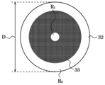
- FIG. 4 is an explanatory diagram showing a state when the niobium layer in Example 1 is viewed from above.
- the niobium layer 32 has a structure in which through holes 33 (groups shown by black circles in the figure) are formed in the thickness direction.
- the niobium layer 32 is formed in a circular shape on the silicon wafer substrate, and has a diameter D of 2.6 mm.
- the niobium layer 32 has a structure in which 7,180 rectangular block regions 36 shown in FIG. 5 are formed.
- FIG. 5 is an explanatory diagram showing a rectangular block area when the niobium layer is viewed from above.
- a through hole 33 having a diameter d of 20.35 ⁇ m is formed at the center.
- the distance s between the outer periphery of the through hole 33 and the outer periphery of the rectangular block region 36 that is closest to the surface is set to 150 nm. That is, the niobium layer 32 as the periodic structure has a structure in which the through-holes 33 as the structure are regularly arranged at intervals of 300 nm.
- the crystal structure is a square lattice, and the lattice constant is 20.65 ⁇ m.
- the square lattice means a structure in which the through holes 33 are arranged in a square lattice shape with respect to the niobium layer 32 in a top view, and the lattice constant is a rectangular block region 36 as a unit lattice. Sometimes, it means the distance between the center of one unit cell and the center of another unit cell adjacent thereto.
- the structure of the periodic structure shown in FIGS. 4 and 5 is formed based on the shape setting of the mask.
- the silicon wafer substrate in this state was cut so as to have the niobium layer as a center.
- a dry etching apparatus (memsstar SVR-vHF, manufactured by Canon Inc.), HF gas is brought into contact with the silicon oxide layer present below the niobium layer through the through-hole, and the silicon oxide layer is removed.
- a dry etching process for partially removing was performed.
- FIG. 1 In FIG. 1
- the silicon oxide layer existing under the regions R 1 and R 2 of the niobium layer 32 in the portion where the rectangular block region 36 is not formed remains after the dry etching process, As the silicon oxide sacrificial layer, the role of supporting the niobium layer 32 at each position of the regions R 1 and R 2 is provided while the lower portion of the rectangular block region 36 is made hollow. Thus, the sample body of Example 1 was produced.
- a measurement test of the electrical resistance and the magnetic flux density of the phononic material according to Example 1 obtained by these steps was performed on the sample body of Example 1 while performing the cooling step and the heating step described below.
- a four-terminal resistance measuring device P102 DC resistance sample pack, manufactured by Quantum Design Japan, Inc.
- the terminals of the four-terminal resistance measuring device are connected to each of the regions R 1 and R 2 in FIG. 4 by two terminals, and a current of 10 ⁇ A is applied between the region R 1 and the region R 2 .
- the electric resistance of the arranged periodic structure can be measured.
- the magnetic flux density is measured by using a Gauss meter (Lake Shore, Gauss meter 425 type) at a distance of about 1 cm from the sample or phononic material in an environment of normal temperature and normal pressure where no external magnetic field exists. I went in.
- Gauss meter Lake Shore, Gauss meter 425 type
- FIG. 6 is a diagram illustrating the state of execution of the cooling step and the heating step in the phononic material according to the first embodiment.
- a first cooling step was performed under the condition that the sample body of Example 1 was cooled from room temperature (300K) to 2K at a cooling rate of 1K / min.
- the first heating step was performed under the condition that the temperature of the sample body of Example 1 was raised from 2K to room temperature at a heating rate of 1 K / min.
- a second cooling step was performed again under the condition that the sample body of Example 1 was cooled from room temperature to 2K at a cooling rate of 1K / min.
- a second heating step was performed again under the condition that the temperature of the sample body of Example 1 was raised from 2K to room temperature at a heating rate of 1 K / min.
- Example 1 a phononic material according to Example 1 was manufactured.
- the characteristics of the phononic material according to the first embodiment will be described with reference to FIG.
- the first cooling step at the beginning of cooling, it is confirmed that the electric resistance value tends to decrease as the temperature decreases. However, after the electric resistance value becomes the lowest around 40K, the electric resistance turns to increase. The phenomenon of minimum resistance was confirmed. Such behavior of the electric resistance value is not observed in ordinary niobium. It is considered that a localized moment of electrons similar to the so-called Kondo effect was generated via the periodic structure.
- the curve of the electric resistance-temperature characteristic is bent around 250 K, and it can be said that a new order that does not exist in ordinary niobium is formed from around 250 K.
- a phenomenon in which the electrical resistance value decreases around 30K, and then turns into a minimum value, which turns into an increase, is confirmed.
- the electric resistance-temperature characteristic curve was the first time. It shows a locus different from the curve of the electric resistance-temperature characteristic in the cooling step.
- the electric resistance value sharply increases from around 50 K, and the behavior of the electric resistance value that cannot be observed from ordinary niobium is confirmed.
- the temperature dependence of the electric resistance value is almost lost from 2K to around 50K, and no metallic behavior of the electric resistance value is observed in a high-temperature environment after 50K.
- the third cooling step it is confirmed that the electric resistance value tends to increase gradually as the temperature decreases.
- a behavior that relatively follows the electric resistance-temperature characteristic curve similar to the electric resistance-temperature characteristic curve in the third cooling step is confirmed.
- the electric resistance values measured in the second cooling step and the heating step were the first time. It has reached a value several hundred times higher than the electric resistance value before the cooling step, and it should be considered that a new material order different from that of ordinary niobium or metal has occurred.
- a magnetic flux density of minus 240 milligauss was measured, and the paramagnetic substance (plus 30 milligauss) before the first cooling step was changed to a diamagnetic substance. The material order is changing.
- Example 2 In order to more accurately investigate the magnetic properties of the sample of Example 1, another sample having the same material and the same structure as the sample of Example 1 (hereinafter, referred to as “sample of Example 2”) is used.
- the sample was placed in a magnetic property measuring apparatus (MPMS, manufactured by Quantum Design Japan, Inc.), and a cooling step and a temperature increasing step were performed under a helium gas atmosphere of about 10 kPa.
- MPMS magnetic property measuring apparatus
- a cooling step and a temperature increasing step were performed under a helium gas atmosphere of about 10 kPa.
- a first cooling step was performed under the condition that the sample body of Example 2 was cooled from room temperature (300 K) to 2 K at a cooling rate of 10 K / min.
- the first heating step was performed under the condition that the temperature of the sample body of Example 2 was raised from 2K to room temperature at a heating rate of 10 K / min. Note that 100 Oe of the external magnetic field remains applied.
- a second cooling step was performed again under the condition that the sample body of Example 2 was cooled from room temperature to 2 K at a cooling rate of 1 K / min. Note that 100 Oe of the external magnetic field remains applied.
- a second heating step was performed again under the condition that the temperature of the sample body of Example 2 was raised from 2K to room temperature at a heating rate of 1 K / min. Note that 100 Oe of the external magnetic field remains applied.
- a third cooling step was performed again under the condition that the sample body of Example 2 was cooled from room temperature to 2 K at a cooling rate of 1 K / min. Note that 100 Oe of the external magnetic field remains applied.
- a third heating step was performed again under the condition that the temperature of the sample body of Example 2 was increased from 2K to room temperature at a heating rate of 1 K / min. Note that 100 Oe of the external magnetic field remains applied.
- the fourth cooling step was performed again under the condition that the sample body of Example 2 was cooled from room temperature to 2 K at a cooling rate of 1 K / min. Note that 100 Oe of the external magnetic field remains applied.
- a fourth heating step was performed again under the condition that the temperature of the sample body of Example 2 was raised from 2K to room temperature at a heating rate of 1 K / min. Note that 100 Oe of the external magnetic field remains applied.
- a fifth cooling step was performed again under the condition that the sample body of Example 2 was cooled from room temperature to 2 K at a cooling rate of 1 K / min. Note that 100 Oe of the external magnetic field remains applied.
- Example 2 Next, a fifth heating step was performed again under the condition that the temperature of the sample body of Example 2 was raised from 2K to room temperature at a heating rate of 1 K / min. Note that 100 Oe of the external magnetic field remains applied. Thus, a phononic material according to Example 2 was manufactured.
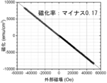
- FIG. 7 is a diagram illustrating the dependence of the magnetization of the phononic material according to Example 2 at room temperature (300 K) on the external magnetic field.
- the magnetic properties are such that an external magnetic field in a direction parallel to the plane direction of the niobium layer is applied to the phononic material according to Example 2 at room temperature from 100 Oe to 50,000 Oe. And applied from 50,000 Oe to -50,000 Oe, then from -50,000 Oe to zero Oe, changing every 500 Oe, and measuring the magnetization of the phononic material according to Example 2 at each stage. .
- the magnetic susceptibility of the phononic material according to Example 2 which is calculated from the magnetization and the gradient of the applied external magnetic field, is ⁇ 0.17, as shown in FIG.
- the negative susceptibility confirms that the phononic material according to Example 2 is a diamagnetic material.
- the phononic material according to Example 2 has a considerably strong diamagnetic susceptibility. You will have.
- the diamagnetic susceptibility of the Meissner effect which is manifested by cooling the superconductor to a low temperature showing superconducting order, is minus one (permanent diamagnetism).
- the phononic material according to Example 2 is completely diamagnetic. A strong diamagnetic susceptibility corresponding to 1/6 is shown at room temperature.
- Example 3 A sample body was manufactured in the same manner as in Example 1 except that a sample body was manufactured by performing i-line lithography processing with a changed mask so as to have the structure shown in FIG. 8 instead of the structure shown in FIG.
- the sample body in Example 3 was produced by the method.
- FIG. 8 is an explanatory view showing a state when the niobium layer in Example 3 is viewed from above, and reference numeral 42 in FIG. 8 indicates a niobium layer, and reference numeral 43 indicates a through hole.
- Symbols J 1 to J 6 indicate terminals for measuring electric resistance.
- the crystal structure is a square lattice
- the lattice constant is 20.65 ⁇ m
- the rectangular block area having the same size as that of the rectangular block area shown in FIG. 5 is formed in common with the sample body in the first embodiment, the number of the rectangular block areas is 350.
- the configuration is different from the sample body (7,180 pieces, circular shape) in the first embodiment in that the entire group of the rectangular block areas is arranged in a rectangular shape.
- Example 3 a measurement test of the electrical resistance of the phononic material according to Example 3 obtained by these steps was performed on the sample body of Example 3 while performing the cooling step and the temperature raising step described below.
- a four-terminal resistance measuring device P106, manufactured by Quantum Design Japan, Inc.
- the terminals J 1 , J 5 , J 2 , and J 3 in FIG. 8 are connected to the terminals I +, I ⁇ , V +, and V ⁇ of the four-terminal resistance measurement device, respectively, and the terminals J 2 -J
- the electrical resistance of the periodic structure disposed between the three could be measured.
- FIG. 9 is a diagram showing the state of execution of the cooling step and the heating step in the phononic material according to Example 3.
- the electric resistance-temperature characteristics at 5K to 100K are shown. It is enlarged and displayed.
- a first cooling step was performed under the condition that the sample body of Example 3 was cooled from room temperature (300 K) to 2 K at a cooling rate of 0.1 K / min.
- the first heating step was performed under the condition that the temperature of the sample body of Example 3 was raised from 2K to room temperature at a heating rate of 0.1 K / min.
- a second cooling step was performed again under the condition that the sample body of Example 3 was cooled from room temperature to 2K at a cooling rate of 0.1 K / min.
- a second heating step was performed again under the condition that the sample body of Example 3 was heated from 2K to room temperature at a heating rate of 0.1 K / min.
- a phononic material according to Example 3 was manufactured.
- the characteristics of the phononic material according to the third embodiment will be described with reference to FIG.
- the first cooling step at the beginning of cooling, a tendency is observed that the electric resistance value decreases as the temperature decreases. However, at around 30 K, a minimum resistance phenomenon that is not observed with ordinary niobium is observed. Further, after the electric resistance value increases at around 10K, the phenomenon of the resistance maxima that changes to one turn and then decreases is confirmed, and then the superconductivity is confirmed from around 8.5K. Next, in the first heating process, an increase in electric resistance was confirmed at around 10K, and thereafter, a decrease in electric resistance was confirmed at around 30K. An increase in the resistance value is confirmed.
- the behavior in which the electric resistance value rises and falls with the temperature rise is not confirmed with ordinary niobium.
- the second cooling step it is confirmed that the electric resistance value sharply increases from around 35K, and the electric resistance value sharply decreases from around 8.5K. Further, the superconductivity confirmed in the first cooling step is not confirmed in a low-temperature environment from around 8.5K.
- the second heating process a behavior similar to the electric resistance-temperature characteristic curve in the second cooling process is confirmed up to around 35K, but the electrical resistance decreases from around 35K in a high-temperature environment. This phenomenon is not confirmed, and it is confirmed that the electric resistance value is higher than the electric resistance value in the second cooling step.
- the electric resistance unique to niobium before the first cooling step is different in each state after the first and second temperature raising steps. It can be said that a new material order having electric resistance and different from ordinary niobium has occurred.
- the phonon in the constituent material constituting the periodic structure interacts with the electrons in the constituent material during cooling, and the behavior of the electrons is restricted. Has become. That is, as shown in FIGS. 6 and 9, in each of the phononic materials according to Examples 1 and 3, since the electrical resistance approaches a constant value on the low temperature side, the mean free path of electrons approaches the minimum value. It shows the region of Joffer-Regel explaining the situation, and it is considered that the so-called minimum metal conductivity is realized.
- the phenomenon in which the mean free path of electrons approaches a minimum value in a material in which magnetic impurities and the like are not mixed in the periodic structure is based on the fact that electrons in the constituent material interact with phonons and are localized. . Further, as shown in FIG. 7, since the phononic material according to Example 2 exhibited a strong diamagnetic susceptibility at room temperature (300 K), unpaired electrons such as conduction electrons were localized and observed with ordinary niobium. It is considered that due to the complete loss of the paramagnetic order, the diamagnetic order obscured by other magnetic orders is manifested in the normal state.
- the number of electrons localized in the niobium atom increases, and in each of the phononic materials according to Examples 1 to 3, the electric resistance finally becomes semiconductor-like behavior.
- the phononic material according to Example 2 will eventually show diamagnetism.
- Such behavior is based on various phenomena such as Mott metal-insulation transition and Anderson localization where electron waves are localized due to the disturbance of the atomic level periodic structure inherent in the constituent material due to formation of through holes. it is conceivable that. If the phenomena occurring in the periodic structure become qualitatively clarified by the progress of future research, the phononic material having the desired physical properties will be developed by predicting the physical properties that will be exhibited by cooling from various physical properties. can do.
Landscapes
- Engineering & Computer Science (AREA)
- Power Engineering (AREA)
- Hard Magnetic Materials (AREA)
- Hall/Mr Elements (AREA)
Abstract
Le problème décrit par la présente invention est de fournir : un matériau phononique qui a des propriétés physiques de magnétisme et/ou de l'électro-conductivité de la substance constitutive qui different des propriétés physiques inhérentes à la substance constitutive ; et son procédé de production. La solution selon l'invention concerne un matériau phononique 1 qui est caractérisé en ce qu'il présente une structure cyclique dans laquelle une structure 3 est disposée de manière cyclique selon un motif régulier dans une substance constitutive 2, et les propriétés physiques du magnétisme et/ou l'électro-conductivité de la substance constitutive 2 dans la structure cyclique diffère des propriétés physiques inhérentes à la substance constitutive lorsqu'elle est comparée à la température ambiante. Le fait que les propriétés physiques de la substance constitutive 2 changent avant et après l'utilisation du refroidissement.
Priority Applications (1)
| Application Number | Priority Date | Filing Date | Title |
|---|---|---|---|
| JP2020527222A JP7145529B2 (ja) | 2018-06-29 | 2019-04-08 | フォノニック材料及びその製造方法 |
Applications Claiming Priority (2)
| Application Number | Priority Date | Filing Date | Title |
|---|---|---|---|
| JP2018-124102 | 2018-06-29 | ||
| JP2018124102 | 2018-06-29 |
Publications (1)
| Publication Number | Publication Date |
|---|---|
| WO2020003689A1 true WO2020003689A1 (fr) | 2020-01-02 |
Family
ID=68987004
Family Applications (1)
| Application Number | Title | Priority Date | Filing Date |
|---|---|---|---|
| PCT/JP2019/015278 Ceased WO2020003689A1 (fr) | 2018-06-29 | 2019-04-08 | Matériau phononique et son procédé de production |
Country Status (2)
| Country | Link |
|---|---|
| JP (1) | JP7145529B2 (fr) |
| WO (1) | WO2020003689A1 (fr) |
Cited By (1)
| Publication number | Priority date | Publication date | Assignee | Title |
|---|---|---|---|---|
| JP2020161530A (ja) * | 2019-03-25 | 2020-10-01 | 国立研究開発法人産業技術総合研究所 | 回路アレイ |
Citations (5)
| Publication number | Priority date | Publication date | Assignee | Title |
|---|---|---|---|---|
| JP2013029463A (ja) * | 2011-07-29 | 2013-02-07 | Canon Inc | 構造体、その製造方法および撮像装置 |
| US8508370B1 (en) * | 2009-02-27 | 2013-08-13 | Sandia Corporation | Synthetic thermoelectric materials comprising phononic crystals |
| JP2014501031A (ja) * | 2010-10-22 | 2014-01-16 | カリフォルニア インスティチュート オブ テクノロジー | 低熱伝導率および熱電性エネルギー転換材料のためのナノメッシュのフォノン性構造 |
| JP2017223644A (ja) * | 2016-06-13 | 2017-12-21 | パナソニックIpマネジメント株式会社 | 赤外線センサ |
| JP2018157018A (ja) * | 2017-03-16 | 2018-10-04 | 国立大学法人 筑波大学 | 熱電変換材料 |
-
2019
- 2019-04-08 WO PCT/JP2019/015278 patent/WO2020003689A1/fr not_active Ceased
- 2019-04-08 JP JP2020527222A patent/JP7145529B2/ja active Active
Patent Citations (5)
| Publication number | Priority date | Publication date | Assignee | Title |
|---|---|---|---|---|
| US8508370B1 (en) * | 2009-02-27 | 2013-08-13 | Sandia Corporation | Synthetic thermoelectric materials comprising phononic crystals |
| JP2014501031A (ja) * | 2010-10-22 | 2014-01-16 | カリフォルニア インスティチュート オブ テクノロジー | 低熱伝導率および熱電性エネルギー転換材料のためのナノメッシュのフォノン性構造 |
| JP2013029463A (ja) * | 2011-07-29 | 2013-02-07 | Canon Inc | 構造体、その製造方法および撮像装置 |
| JP2017223644A (ja) * | 2016-06-13 | 2017-12-21 | パナソニックIpマネジメント株式会社 | 赤外線センサ |
| JP2018157018A (ja) * | 2017-03-16 | 2018-10-04 | 国立大学法人 筑波大学 | 熱電変換材料 |
Cited By (2)
| Publication number | Priority date | Publication date | Assignee | Title |
|---|---|---|---|---|
| JP2020161530A (ja) * | 2019-03-25 | 2020-10-01 | 国立研究開発法人産業技術総合研究所 | 回路アレイ |
| JP7228886B2 (ja) | 2019-03-25 | 2023-02-27 | 国立研究開発法人産業技術総合研究所 | 回路アレイ |
Also Published As
| Publication number | Publication date |
|---|---|
| JP7145529B2 (ja) | 2022-10-03 |
| JPWO2020003689A1 (ja) | 2021-04-22 |
Similar Documents
| Publication | Publication Date | Title |
|---|---|---|
| Córdoba et al. | Three-dimensional superconducting nanohelices grown by He+-focused-ion-beam direct writing | |
| US9394624B2 (en) | Method for making topological insulator structure | |
| US20140179026A1 (en) | Method for generating quantized anomalous hall effect | |
| KR101894828B1 (ko) | 정보 기록 장치, 정보 기록 방법 및 정보 재생 방법 | |
| US20140175382A1 (en) | Electrical device | |
| JP6219819B2 (ja) | 磁歪層システム | |
| US20140175373A1 (en) | Topological insulator structure | |
| WO2013125101A1 (fr) | Mémoire spintronique et circuit spintronique | |
| US10403810B2 (en) | Magnetic diode in artificial magnetic honeycomb lattice | |
| Li et al. | Enhanced anomalous Nernst effect by tuning the chemical potential in the topological kagome ferromagnet Fe 3 Sn 2 | |
| Zhang et al. | Topological Anderson insulator via disorder-recovered average symmetry | |
| JP7145529B2 (ja) | フォノニック材料及びその製造方法 | |
| Anwar et al. | Inducing supercurrents in thin films of ferromagnetic CrO2 | |
| Wang et al. | Quantum anomalous Hall effect in twisted bilayer graphene | |
| Wang et al. | Experimental realization of antiferromagnetic Ising ground state on the triangular lattice | |
| Herring | The flux lattice in a deformed type II superconductor | |
| WO2021132358A1 (fr) | Matériau phononique et son procédé de production | |
| Lin et al. | Interfacial phase competition induced Kondo-like effect in manganite-insulator composites | |
| Shigeta et al. | Fabrication and characterization of epitaxial films of superconductor NbN and highly spin-polarized Heusler alloy Co2Fe0. 4Mn0. 6Si | |
| Fan et al. | Enhanced Magnetoresistance Effect in Graphene Coupled to a Ferromagnetic Oxide with Charge Orbital Ordering | |
| JP7228886B2 (ja) | 回路アレイ | |
| Pahari | GROWTH, MAGNETIZATION AND TRANSPORT PROPERTIES OF Co2FeAl-BASED MULTILAYERS | |
| Zhang et al. | Metal-insulator phase separation in KTaO3-based two-dimensional electron gas | |
| Zhao | Exploration of High Chern Number and High Temperature Quantum Anomalous Hall Effect | |
| Guo et al. | Topological phase transitions induced by correlated magnetic disorder in two-dimensional quantum anomalous Hall system |
Legal Events
| Date | Code | Title | Description |
|---|---|---|---|
| 121 | Ep: the epo has been informed by wipo that ep was designated in this application |
Ref document number: 19826248 Country of ref document: EP Kind code of ref document: A1 |
|
| ENP | Entry into the national phase |
Ref document number: 2020527222 Country of ref document: JP Kind code of ref document: A |
|
| NENP | Non-entry into the national phase |
Ref country code: DE |
|
| 122 | Ep: pct application non-entry in european phase |
Ref document number: 19826248 Country of ref document: EP Kind code of ref document: A1 |