WO2020003783A1 - 撮像素子、撮像装置、及び、電子機器 - Google Patents
撮像素子、撮像装置、及び、電子機器 Download PDFInfo
- Publication number
- WO2020003783A1 WO2020003783A1 PCT/JP2019/019102 JP2019019102W WO2020003783A1 WO 2020003783 A1 WO2020003783 A1 WO 2020003783A1 JP 2019019102 W JP2019019102 W JP 2019019102W WO 2020003783 A1 WO2020003783 A1 WO 2020003783A1
- Authority
- WO
- WIPO (PCT)
- Prior art keywords
- vertical signal
- pixel
- wiring layer
- signal line
- signal lines
- Prior art date
- Legal status (The legal status is an assumption and is not a legal conclusion. Google has not performed a legal analysis and makes no representation as to the accuracy of the status listed.)
- Ceased
Links
Images


Classifications
-
- H—ELECTRICITY
- H04—ELECTRIC COMMUNICATION TECHNIQUE
- H04N—PICTORIAL COMMUNICATION, e.g. TELEVISION
- H04N25/00—Circuitry of solid-state image sensors [SSIS]; Control thereof
- H04N25/70—SSIS architectures; Circuits associated therewith
- H04N25/76—Addressed sensors, e.g. MOS or CMOS sensors
- H04N25/78—Readout circuits for addressed sensors, e.g. output amplifiers or A/D converters
-
- H—ELECTRICITY
- H10—SEMICONDUCTOR DEVICES; ELECTRIC SOLID-STATE DEVICES NOT OTHERWISE PROVIDED FOR
- H10F—INORGANIC SEMICONDUCTOR DEVICES SENSITIVE TO INFRARED RADIATION, LIGHT, ELECTROMAGNETIC RADIATION OF SHORTER WAVELENGTH OR CORPUSCULAR RADIATION
- H10F39/00—Integrated devices, or assemblies of multiple devices, comprising at least one element covered by group H10F30/00, e.g. radiation detectors comprising photodiode arrays
- H10F39/80—Constructional details of image sensors
- H10F39/802—Geometry or disposition of elements in pixels, e.g. address-lines or gate electrodes
-
- H—ELECTRICITY
- H10—SEMICONDUCTOR DEVICES; ELECTRIC SOLID-STATE DEVICES NOT OTHERWISE PROVIDED FOR
- H10F—INORGANIC SEMICONDUCTOR DEVICES SENSITIVE TO INFRARED RADIATION, LIGHT, ELECTROMAGNETIC RADIATION OF SHORTER WAVELENGTH OR CORPUSCULAR RADIATION
- H10F39/00—Integrated devices, or assemblies of multiple devices, comprising at least one element covered by group H10F30/00, e.g. radiation detectors comprising photodiode arrays
- H10F39/80—Constructional details of image sensors
- H10F39/811—Interconnections
-
- H—ELECTRICITY
- H10—SEMICONDUCTOR DEVICES; ELECTRIC SOLID-STATE DEVICES NOT OTHERWISE PROVIDED FOR
- H10P—GENERIC PROCESSES OR APPARATUS FOR THE MANUFACTURE OR TREATMENT OF DEVICES COVERED BY CLASS H10
- H10P14/00—Formation of materials, e.g. in the shape of layers or pillars
- H10P14/40—Formation of materials, e.g. in the shape of layers or pillars of conductive or resistive materials
-
- H—ELECTRICITY
- H10—SEMICONDUCTOR DEVICES; ELECTRIC SOLID-STATE DEVICES NOT OTHERWISE PROVIDED FOR
- H10W—GENERIC PACKAGES, INTERCONNECTIONS, CONNECTORS OR OTHER CONSTRUCTIONAL DETAILS OF DEVICES COVERED BY CLASS H10
- H10W20/00—Interconnections in chips, wafers or substrates
- H10W20/01—Manufacture or treatment
-
- H—ELECTRICITY
- H10—SEMICONDUCTOR DEVICES; ELECTRIC SOLID-STATE DEVICES NOT OTHERWISE PROVIDED FOR
- H10W—GENERIC PACKAGES, INTERCONNECTIONS, CONNECTORS OR OTHER CONSTRUCTIONAL DETAILS OF DEVICES COVERED BY CLASS H10
- H10W20/00—Interconnections in chips, wafers or substrates
- H10W20/40—Interconnections external to wafers or substrates, e.g. back-end-of-line [BEOL] metallisations or vias connecting to gate electrodes
Definitions
- the present disclosure relates to an imaging device, an imaging device, and an electronic device.
- an imaging device having an imaging element such as a complementary metal oxide semiconductor (CMOS) sensor is used.
- the imaging element is configured by combining a photoelectric conversion unit including a photodiode (Photo Diode: PD), a floating diffusion region (FD) in which photoelectrically converted charges are transferred, a plurality of transistors, and the like. It has pixels. Then, an image is constructed based on signals output from a plurality of pixels arranged in a two-dimensional matrix. The signals output from the pixels are A / D converted in parallel by a plurality of A / D (Analog to Digital) converters arranged for each pixel column, and output as digital signals.
- a / D Analog to Digital
- a frame rate of 120 fps has become common in high-end display devices.
- an image sensor capable of imaging at a high frame rate such as 960 fps is also required. Since imaging at a high frame rate also reduces so-called focal plane distortion, there is an increasing demand for imaging at a high frame rate even in imaging of a sports scene in which a fast-moving subject needs to be captured as a still image. ing. Therefore, a plurality of vertical signal lines for reading a signal from a pixel are arranged for each pixel column (for example, see Patent Document 1 and Non-Patent Document 1). Further, in order to arrange a large number of vertical signal lines in each pixel column, it has been proposed to arrange a vertical signal line in each of a plurality of wiring layers stacked on a pixel (for example, Non-Patent Document 1). See).
- the vertical signal line is usually connected to the pixel via a via provided in the wiring layer. Is done.
- it is necessary to connect vias to each vertical signal line so that it is not possible to arrange orthogonal signal lines in a plurality of wiring layers so as to overlap.
- the vertical signal lines and the pixels are not hindered.
- it can be electrically connected.
- the present disclosure relates to an image sensor capable of electrically connecting a vertical signal line and a pixel without hindrance even if the orthogonal projections of the vertical signal lines are arranged so as to overlap in a plurality of wiring layers. It is an object of the present invention to provide an imaging device provided with the electronic device and an electronic device provided with the imaging device.
- the imaging device for achieving the above object, A pixel array section in which pixels are arranged in a matrix, A plurality of vertical signal lines provided for each pixel column; And The plurality of vertical signal lines provided for each pixel column are arranged on a plurality of wiring layers stacked on the pixel, and are arranged so that orthogonal projections of the vertical signal lines on the plurality of wiring layers overlap.
- a connection portion for connecting a vertical signal line corresponding to the pixel to the pixel is provided in the wiring layer, The pixel signal is taken out of the vertical signal line via the connection, An image sensor.
- An imaging device for achieving the above object, A pixel array section in which pixels are arranged in a matrix, A plurality of vertical signal lines provided for each pixel column; And The plurality of vertical signal lines provided for each pixel column are arranged on a plurality of wiring layers stacked on the pixel, and are arranged so that orthogonal projections of the vertical signal lines on the plurality of wiring layers overlap.
- a connection portion for connecting a vertical signal line corresponding to the pixel to the pixel is provided in the wiring layer, The pixel signal is taken out of the vertical signal line via the connection, Having an image sensor configured as An imaging device.
- a pixel array section in which pixels are arranged in a matrix, A plurality of vertical signal lines provided for each pixel column; And The plurality of vertical signal lines provided for each pixel column are arranged on a plurality of wiring layers stacked on the pixel, and are arranged so that orthogonal projections of the vertical signal lines on the plurality of wiring layers overlap.
- a connection portion for connecting a vertical signal line corresponding to the pixel to the pixel is provided in the wiring layer, The pixel signal is taken out of the vertical signal line via the connection, Having an image sensor configured as Electronic equipment.
- FIG. 1 is a schematic diagram for explaining a configuration example of an image sensor.
- FIG. 2 is a schematic circuit diagram for explaining a configuration example of a pixel of the image sensor.
- FIG. 3 is a schematic perspective view for explaining the structure of various wirings in the wiring layer of the reference example.
- FIG. 4 is a schematic perspective view for explaining the structure of each layer in the wiring layer of the reference example.
- FIG. 5 is a schematic plan view for explaining the relationship between the orthogonal projection of the laminated state in the wiring layer of the reference example and the structure of each layer.
- FIG. 6 is a schematic perspective view for explaining the structure of various wirings in a wiring layer used in the image sensor according to the first embodiment.
- FIG. 1 is a schematic diagram for explaining a configuration example of an image sensor.
- FIG. 2 is a schematic circuit diagram for explaining a configuration example of a pixel of the image sensor.
- FIG. 3 is a schematic perspective view for explaining the structure of various wirings in the wiring layer of the reference example.
- FIG. 7 is a schematic perspective view for explaining the structure of each layer in the wiring layer used in the image sensor according to the first embodiment.
- FIG. 8 is a schematic plan view for explaining the relationship between the orthogonal projection of the stacked state in the wiring layer used in the image sensor according to the first embodiment and the structure of each layer.
- FIG. 9 is a schematic perspective view for explaining a connection relationship between a second-layer vertical signal line and a pixel in a wiring layer used in the image sensor according to the first embodiment.
- FIG. 10A is a schematic end view for explaining the connection relationship between the vertical signal line VSL21 and the pixel.
- FIG. 10B is a schematic end view for explaining the connection relationship between the vertical signal line VSL22 and the pixel.
- FIG. 11A is a schematic end view for explaining the connection relationship between the vertical signal line VSL11 and the pixel.
- FIG. 11B is a schematic end view for explaining the connection relationship between the vertical signal line VSL12 and the pixel.
- FIG. 12 is a schematic plan view for explaining the relationship between the orthogonal projection of the stacked state in the wiring layer according to the first modification and the structure of each layer.
- FIG. 13A is a schematic end view for explaining the connection relationship between the vertical signal line VSL11 and the pixel.
- FIG. 13B is a schematic end view for explaining the connection relationship between the vertical signal line VSL12 and the pixel.
- FIG. 14 is a schematic perspective view for explaining the structure of each layer in the wiring layer according to the second modification.
- FIG. 15 is a schematic perspective view for explaining the structure of each layer in the wiring layer according to the second modification.
- FIG. 16 is a schematic plan view for explaining the relationship between the orthogonal projection of the stacked state in the wiring layer according to the second modification and the structure of each layer.
- FIG. 17 is a schematic perspective view for explaining a connection relationship between a vertical signal line and a pixel in a third wiring layer according to the second modification.
- FIG. 18 is a schematic end view for explaining the connection relationship between the vertical signal line VSL31 and the pixel.
- FIG. 19 is a schematic end view for explaining the connection relationship between the vertical signal line VSL32 and the pixel.
- FIG. 20 is a schematic plan view for explaining the relationship between the orthogonal projection of the stacked state in the wiring layer according to the third modification and the structure of each layer.
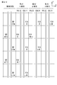
- FIG. 21 is a table for explaining the relationship between the number of layers and the number of wires that can be wired in the wiring layers used in the image sensor according to the first embodiment.
- FIG. 22 is a schematic perspective view for explaining a connection relationship between a vertical signal line and a pixel in a wiring layer used in the image sensor according to the second embodiment.
- FIG. 23 is a schematic perspective view for explaining the structure of each layer in a wiring layer used in the imaging device according to the second embodiment.
- FIG. 24 is a schematic plan view for explaining the relationship between the orthogonal projection of the stacked state in the wiring layer used in the image sensor according to the second embodiment and the structure of each layer.
- FIG. 25 is a schematic end view for explaining the connection relationship between the vertical signal line VSL31 and the pixel shown in FIG.
- FIG. 26 is a schematic perspective view for explaining a connection relationship between a vertical signal line and a pixel in a wiring layer.
- FIG. 27 is a schematic end view for explaining the connection relationship between the vertical signal line VSL21 and the pixel shown in FIG.
- FIG. 28 is a schematic perspective view for explaining a connection relationship between a vertical signal line and a pixel in a wiring layer.
- FIG. 29 is a schematic end view for explaining the connection relationship between the vertical signal line VSL11 and the pixel shown in FIG.
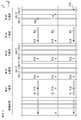
- FIG. 30 is a table for explaining the relationship between the number of layers in the wiring layer used in the image sensor according to the second embodiment and the number of wires that can be wired.
- FIG. 31 is a schematic perspective view for explaining a connection relationship between a vertical signal line and a pixel in a wiring layer used in the image sensor according to the third embodiment.
- FIG. 32 is a schematic end view for explaining the structure of each layer in the wiring layer used in the image sensor according to the third embodiment.
- FIG. 33 is a schematic perspective view for explaining a connection relationship between a vertical signal line and a pixel in a wiring layer used in an imaging device according to the fourth embodiment.
- FIG. 34 is a schematic plan view for explaining the relationship between the orthogonal projection of the stacked state in the wiring layer used in the image sensor according to the fourth embodiment and the structure of each layer.
- FIG. 35 is a table for explaining the relationship between the number of layers and the number of wires that can be wired in the wiring layers used in the image sensor according to the fourth embodiment.
- FIG. 36 is a schematic perspective view for explaining a connection relationship between a vertical signal line and a pixel in a wiring layer used in the imaging device according to the fifth embodiment.
- FIG. 37 is a schematic end view for explaining the connection relationship between the vertical scanning line VSL21 and the pixel shown in FIG. FIG.
- FIG. 38 is a table for explaining the relationship between the number of layers in the wiring layer used in the imaging device according to the fifth embodiment and the number of wires that can be wired.
- FIG. 39 is a schematic perspective view for explaining a connection relationship between a vertical signal line and a pixel in a wiring layer used in an imaging device according to the sixth embodiment.
- FIG. 40 is a schematic perspective view for explaining the connection relationship between the vertical signal line and the pixel in the wiring layer used in the imaging device according to the sixth embodiment, following FIG.
- FIG. 41 is a block diagram illustrating an example of a schematic configuration of a vehicle control system.
- FIG. 42 is an explanatory diagram illustrating an example of the installation positions of the outside-of-vehicle information detection unit and the imaging unit.
- Imaging device An imaging device according to the present disclosure, an imaging device used in an imaging device according to the present disclosure, and an imaging device used in an electronic device according to the present disclosure (hereinafter, these may be simply referred to as an imaging device according to the present disclosure. )
- a via connected to the vertical signal line is provided as a connection portion, Pixel signals are extracted from vertical signal lines via vias. It can be configured.
- a relay line extending in a direction orthogonal to a direction in which the vertical signal line extends is arranged as a connection portion in each of the pixels as a connection part in a part of the plurality of stacked wiring layers. Pixel signals are extracted from the vertical signal lines via vias and relay lines. It can be configured.
- a relay line extending in a direction orthogonal to a direction in which the vertical signal line extends is arranged for each pixel in a state connected to the pixel as a connection portion. ing, It can be configured.
- the trunk line is arranged so as to cross only the vertical signal line in a range that may be related to the connection, It can be configured. Furthermore, Further provided is a shield wiring arranged so as to cross only the vertical signal lines in a range that cannot be related to the connection, extending on the same line as the relay line, and applying a predetermined fixed voltage. It can be configured.
- the wiring layer on which the relay line is disposed is used for connecting a vertical signal line in one of the upper wiring layer and the lower wiring layer stacked adjacent to the wiring layer on which the relay line is disposed. Is provided as, It can be configured.
- the wiring layer on which the relay line is disposed is provided for connection with the vertical signal line in the upper wiring layer and the lower wiring layer stacked adjacent to the wiring layer on which the relay line is disposed, It can be configured.
- the vertical signal lines in the upper wiring layer and the lower wiring layer are arranged so that the orthogonal projection of the vertical signal line to the wiring layer does not overlap. It can be configured.
- the vertical signal lines are arranged to bypass portions of the via that are not involved in the connection to the pixel, It can be configured.
- the vertical signal lines in the two wiring layers stacked adjacent to each other are arranged so that the orthogonal projections of the vertical signal lines on the wiring layers do not overlap. It can be configured.
- the surface-illuminated imaging device has a configuration in which light is incident from the wiring layer side, there is a problem that the arrangement of various wirings is limited in order to secure an optical path.
- the back-illuminated imaging device there is no restriction such as securing an optical path. Therefore, from the viewpoint of increasing the number of vertical signal lines, it is preferable that the imaging device be configured as a back-illuminated type.
- the wiring layer can be formed by, for example, forming an opening or the like as appropriate after forming an insulating material layer, and then performing appropriate patterning after forming a conductive material over the entire surface.
- the insulating material layer can be formed using, for example, a SiO x -based material (a material constituting a silicon-based oxide film), SiN, SiON, SiOC, SiOF, SiCN, or organic SOG.
- the conductive material for example, copper, a copper alloy, or aluminum can be used as the conductive material.
- the wiring layer is formed by a known method such as various chemical vapor deposition methods or various physical vapor deposition methods, a combination of a lithography technique and an etching technique, a known technique such as a lift-off method, a combination of a plating method and a damascene method. Method.
- the pixel array section can be formed on a semiconductor substrate made of, for example, silicon.
- the pixel can be composed of a photoelectric conversion unit and various circuits for driving the photoelectric conversion unit.
- the configuration of the pixel is not particularly limited, and may be, for example, a floating diffusion region accumulation type configuration or a memory accumulation type configuration.
- Various circuits for driving the pixel array unit may be integrated with the pixel array unit or may be separate units. For example, a part of various circuits may be configured separately from the pixel array unit.
- an imaging device including the imaging element according to the present disclosure an imaging device such as a digital still camera or a digital video camera can be exemplified.
- an electronic device including the imaging element according to the present disclosure various electronic devices such as a mobile phone having an imaging function or another device having an imaging function can be exemplified.
- the first embodiment relates to an imaging device, an imaging device, and an electronic device according to the present disclosure.
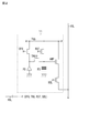
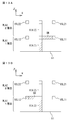
- FIG. 1 is a schematic diagram for explaining a configuration of a CMOS image sensor as an image sensor to which the present disclosure is applied.
- the imaging device 1 A pixel array unit 10 in which pixels 11 are arranged in a matrix, a plurality of vertical signal lines VSL provided in pixel column units, a vertical drive circuit 20, a horizontal drive circuit 30 for driving the pixel array unit 10, A signal processing unit 40 is provided. These operations are controlled by a control circuit (not shown).
- a plurality of vertical signal lines VSL provided in pixel column units are arranged in a plurality of wiring layers stacked on the pixels 11.
- the first wiring layer closest to the pixel side is denoted by reference numeral WLA1
- the second wiring layer is denoted by reference numeral WLA2.
- WLA1 the first wiring layer closest to the pixel side
- WLA2 the second wiring layer
- the pixel array unit 10 includes pixels 11 each having a photoelectric conversion unit and a floating diffusion region to which the photoelectrically converted charge is transferred, which are arranged in a matrix. Each pixel 11 is connected to the vertical drive circuit 20 via a control line HSL for each row. Each pixel 11 is connected to the horizontal drive circuit 30 via the vertical signal line VSL for each column.
- the pixel 11 outputs a pixel signal at a level corresponding to the amount of light received.
- An image of the subject is constituted by the pixel signals.
- the pixel 11 includes a photoelectric conversion unit including a photodiode, a floating diffusion region to which charges from the photoelectric conversion unit are transferred, and a transistor for driving the pixel 11.
- a photoelectric conversion unit including a photodiode, a floating diffusion region to which charges from the photoelectric conversion unit are transferred, and a transistor for driving the pixel 11.
- a configuration can be adopted in which these components are formed in a p-type well provided in an n-type semiconductor substrate.
- the vertical drive circuit 20 supplies a drive signal for sequentially driving the pixels 11 of the pixel array unit 10 row by row to the pixels 11 via the control lines HSL.
- FIG. 1 shows one control line HSL for each pixel row.
- a plurality of types of control lines are arranged corresponding to one pixel row.
- the signal level and the reset level output from the pixel 11 are sent to the horizontal drive circuit 30 via the vertical signal line VSL.
- Each of the plurality of vertical signal lines VSL is connected to a pixel group having a predetermined relationship among the pixels 11 forming the pixel column.
- the horizontal driving circuit 30 performs A / D conversion after performing double sampling (DDS) based on the signal output from the pixel 11.
- the horizontal drive circuit 30 can be configured to perform, for example, DDS processing in parallel for each vertical signal line VSL. Then, a pixel signal is output from the horizontal drive circuit 30 to the signal processing unit 40.
- the signal processing unit 40 performs, for example, various kinds of signal processing on the pixel signal from the horizontal drive circuit 30 to generate an image output.
- the signal processing unit 40 may be formed integrally with the semiconductor substrate on which the pixel array unit 10 is formed, or may be provided on another substrate. Further, the signal processing unit 40 may be a process by a DSP or software.
- the vertical drive circuit 20 is configured by a logic circuit such as a shift register and an address decoder, and drives each pixel 11 of the pixel array unit 10 simultaneously for all pixels or in units of rows. For example, it is possible to adopt a configuration in which resetting, exposure, and transfer of charge of the pixel 11 are performed simultaneously for all pixels, and reading is performed in units of rows.
- FIG. 2 is a schematic circuit diagram for explaining a configuration example of the pixel of the image sensor.
- Pixel 11 is An initialization transistor for applying a predetermined voltage to the photoelectric conversion unit PD; A transfer transistor for transferring the photoelectrically converted charge to the floating diffusion region FD, A reset transistor for applying a predetermined voltage to the floating diffusion region FD, An amplification transistor in which the voltage of the floating diffusion region FD is applied to the gate electrode; and A selection transistor for connecting the amplification transistor and the vertical signal line VSL, , Five transistors (represented by symbols OFG, TRG, RST, AMP, and SEL, respectively), a photoelectric conversion unit PD including a photodiode, and a floating diffusion region FD.
- a constant voltage (for example, a ground voltage) is supplied to one end (anode side) of the photoelectric conversion unit PD and one end of the floating diffusion region FD.
- the power supply line to which the drive voltage is supplied and the other end (cathode side) of the photoelectric conversion unit PD are connected via the initialization transistor OFG.
- the power supply line to which the drive voltage is supplied and the other end of the floating diffusion region FD are connected via a reset transistor RST.
- the other end of the photoelectric conversion unit PD and the other end of the floating diffusion region FD are connected via a transfer transistor TRG.
- One end of the amplification transistor AMP is connected to a power supply line to which a drive voltage is supplied.
- the other end of the amplification transistor AMP and the vertical signal line VSL are connected via a selection transistor SEL.
- the gate electrode of the amplification transistor AMP is connected to the other end of the floating diffusion region FD.
- control lines connected to the gate electrodes of the transistors OFG, TRG, RST, and SEL are referred to as a control line HSL (OFG), a control line HSL (TRG), a control line HSL (RST), and a control line HSL, respectively. (SEL).
- control lines HSL (OFG) of all rows are at a high level (in other words, the state where the voltage V DD is applied via the initialization transistor OFG and the photoelectric conversion unit PD is reset),
- the control lines HSL (OFG) of all rows are set to a low level collectively. Thus, exposure is started in all pixels.
- control lines HSL (TRG) of all rows are set to a high level for a predetermined period.
- the transfer transistor TRG becomes conductive, and the photoelectrically converted charge is transferred to the floating diffusion region FD and held.
- the pixel signal is read. Specifically, the control line HSL (SEL) of the row to be read is set to the high level for a predetermined period. As a result, the amplification transistor AMP is connected to the vertical signal line VSL via the conductive selection transistor SEL. Then, during that period, the control line HSL (RST) is set to the high level for a certain period. With this operation, the signal level and the reset level are read.
- the signal level and the reset level read via the vertical signal line VSL are respectively controlled by the gate voltage of the amplification transistor AMP.
- the horizontal drive circuit 30 calculates a difference between the reset level and the signal level, and uses the difference as a video signal V OUT .
- the basic operation of the pixel 11 has been described above. Note that the above-described configuration of the pixel is an example, and various configurations such as a configuration in which OFG is omitted and a configuration in which a plurality of transistors SEL are provided can be employed.
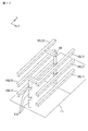
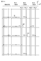
- FIG. 3 the structure of a wiring layer according to a reference example will be described with reference to FIGS. 3, 4, and 5.
- FIG. 3 is a schematic perspective view for explaining the structure of various wirings in the wiring layer of the reference example.
- FIG. 4 is a schematic perspective view for explaining the structure of each layer in the wiring layer of the reference example.
- FIG. 5 is a schematic plan view for explaining the relationship between the orthogonal projection of the laminated state in the wiring layer of the reference example and the structure of each layer.
- illustration of an insulating material forming a wiring layer is omitted in these drawings. The same applies to other drawings described later.
- each vertical signal line VSL is arranged for one pixel column.
- two of the four vertical signal lines VSL are arranged in the second wiring layer WLA2, and the remaining two are arranged in the third wiring layer WLA3.
- a relay line CL connected to the pixel 11 provided for each pixel 11 is arranged in the first wiring layer WLA1 located closest to the pixel.
- Reference numeral VIA indicates a connection via provided in the wiring layer.
- the vertical signal line VSL and the relay line CL are connected by vias.
- the connection is also made via a via provided in the wiring layer.
- the vertical signal lines VSL of the second layer and the vertical signal lines VSL of the third layer are arranged so that the orthogonal projections do not overlap.
- the fourth wiring layer is further formed to increase the vertical signal lines VSL
- the vertical signal lines VSL cannot be arranged so that the orthogonal projections overlap. This is because it is necessary to connect a via to the vertical signal line VSL in the fourth layer, but it is not possible to arrange the via in a state of being electrically independent from the vertical signal line VSL in the lower layer.
- the space is provided between the vertical signal line VSL of the second layer and the via so as to secure a minimum space (represented by a symbol MP). Therefore, it is impossible to further arrange the vertical signal lines VSL between the adjacent vertical signal lines VSL.
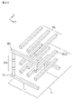
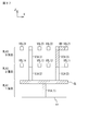
- FIG. 6 is a schematic perspective view for explaining the structure of various wirings in the wiring layer used in the image sensor according to the first embodiment.
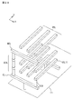
- FIG. 7 is a schematic perspective view for explaining the structure of each layer in the wiring layer.
- FIG. 8 is a schematic plan view for explaining the relationship between the orthogonal projection of the stacked state in the wiring layer and the structure of each layer.
- the plurality of vertical signal lines VSL provided in pixel column units are arranged in the plurality of wiring layers stacked on the pixel 11.
- the wiring layers have a two-layer configuration (WLA1, WLA2), and two vertical signal lines VSL are arranged in each layer.
- a via connected to the vertical signal line VSL is provided in the wiring layer as a connection portion, and the signal of the pixel 11 is extracted from the vertical signal line VSL via the via.
- Vias constituting a connection portion provided in the wiring layer are arranged between the two vertical signal lines VSL.
- the vertical signal line VSL and the via provided in the wiring layer are connected by a branch wiring BR extending in a direction orthogonal to the direction in which the vertical signal line VSL extends. Vias are also formed in the first wiring layer WLA1 corresponding to the vias connected to the second vertical signal line VSL.
- the vertical signal line VSL and the pixel 11 can be connected without providing a relay line in the first layer. Then, as shown in FIG. 8, the vertical signal lines VSL can be arranged so that the orthogonal projections of the vertical signal lines VSL on the plurality of wiring layers overlap.
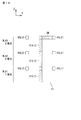
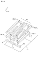
- FIG. 9 is a schematic perspective view for explaining the connection relationship between the vertical signal lines of the second layer and the pixels.
- FIG. 10A is a schematic end view for explaining the connection relationship between the vertical signal line VSL21 and the pixel.
- FIG. 10B is a schematic end view for explaining the connection relationship between the vertical signal line VSL22 and the pixel.
- VIA (1) the via of the first layer
- VIA (2) the via of the second layer
- the second-layer vertical signal line VSL is connected to the corresponding pixel 11 by the second-layer branch wiring BR and vias provided in the first and second layers. Is done.
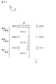
- FIG. 11A is a schematic end view for explaining the connection relationship between the vertical signal line VSL11 and the pixel.
- FIG. 11B is a schematic end view for explaining the connection relationship between the vertical signal line VSL12 and the pixel.
- the first-layer vertical signal line VSL is connected to the corresponding pixel 11 by the first-layer branch wiring BR and the via provided in the first-layer.
- the vertical signal lines VSL can be arranged so that the orthogonal projections of the vertical signal lines VSL on the plurality of wiring layers overlap. Furthermore, the vertical signal line VSL and the pixel 11 can be connected without providing a relay line in the first layer.
- FIG. 12 is a schematic plan view for explaining the relationship between the orthogonal projection of the stacked state in the wiring layer according to the first modification and the structure of each layer.
- FIG. 13A is a schematic end view for explaining the connection relationship between the vertical signal line VSL11 and the pixel.
- FIG. 13B is a schematic end view for explaining the connection relationship between the vertical signal line VSL12 and the pixel.
- the number of vertical signal lines can be increased without limitation by increasing the number of wiring layers to be stacked.
- a second modified example in which the wiring layer has a three-layer structure will be described.
- FIG. 14 is a schematic perspective view for explaining the structure of each layer in the wiring layer according to the second modification.
- FIG. 15 is a schematic perspective view for explaining the structure of each layer in the wiring layer.
- FIG. 16 is a schematic plan view for explaining the relationship between the orthogonal projection of the stacked state in the wiring layer and the structure of each layer.
- the second modified example has a configuration in which third-layer vertical signal lines VSL31, VSL32, and the like are further added to the configuration described with reference to FIGS.
- FIG. 17 is a schematic perspective view for explaining a connection relationship between a vertical signal line and a pixel in a third wiring layer according to the second modification.
- FIG. 18 is a schematic end view for explaining the connection relationship between the vertical signal line VSL31 and the pixel.
- FIG. 19 is a schematic end view for explaining the connection relationship between the vertical signal line VSL32 and the pixel.
- the vertical signal line VSL in the third layer corresponds to the branch wiring BR in the third layer and vias provided in the first, second, and third layers. Connected to pixel 11.
- the connection relationship between the second-layer and third-layer vertical signal lines VSL and the pixels 11 is the same as the connection relationship described with reference to FIGS. 9 to 12, and a description thereof will be omitted.
- the via forming the connection portion provided in the wiring layer is arranged between the two vertical signal lines VSL. Therefore, the position where the via is connected to the pixel 11 is constant regardless of the pixel 11.
- FIG. 20 is a schematic plan view for explaining the relationship between the orthogonal projection of the stacked state in the wiring layer according to the third modification and the structure of each layer.
- the vias are arranged outside the two vertical signal lines VSL.
- the positions where the vias are connected to the pixels 11 are alternately arranged for each pixel 11.
- the via and the vertical signal line VSL are connected by a branch wiring BR.
- the first-layer vertical signal line VSL is connected to the corresponding pixel 11 by the first-layer branch wiring BR and the via provided in the first-layer.
- the second-layer vertical signal line VSL is connected to the corresponding pixel 11 by the second-layer branch wiring BR and vias provided in the first and second layers.
- the third-layer vertical signal line VSL is connected to the corresponding pixel 11 by a third-layer branch wiring BR and vias provided in the first, second, and third layers.
- the number of vertical signal lines in each layer is basically limited to two.
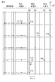
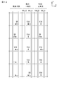
- FIG. 21 shows the relationship between the total number of wiring layers and the total number of vertical signal lines with respect to the maximum number of wirings that can be arranged in each layer at the minimum pitch of the design rule.
- the second embodiment also relates to an imaging device, an imaging device, and an electronic device according to the present disclosure.
- the number of vertical signal lines arranged in the wiring layer is limited. In the second embodiment, three or more vertical signal lines can be arranged in the wiring layer.
- FIG. 22 is a schematic perspective view for explaining a connection relationship between a vertical signal line and a pixel in a wiring layer used in the imaging device according to the second embodiment.
- FIG. 23 is a schematic perspective view for explaining the structure of each layer in the wiring layer.
- FIG. 24 is a schematic plan view for explaining the relationship between the orthogonal projection of the stacked state in the wiring layer and the structure of each layer.
- the plurality of vertical signal lines VSL provided in the pixel column unit are arranged in the plurality of wiring layers stacked on the pixel 11.
- the wiring layer has a five-layer configuration, and three vertical signal lines VSL are arranged in each of the second-layer WLA2, the third-layer WLA3, and the fifth-layer WLA5.
- the orthogonal projections of the vertical signal lines VSL on the plurality of wiring layers are all arranged so as to overlap.
- a via connected to the vertical signal line VSL is provided as a connection portion in the wiring layer.
- some of the stacked wiring layers (the fourth layer and the first layer in the example shown in the drawing) among the plurality of stacked wiring layers are provided as connecting portions.
- a relay line extending in a direction orthogonal to the direction in which the vertical signal line VSL extends is arranged for each pixel 11.
- a relay line extending in a direction orthogonal to the direction in which the vertical signal line VSL extends extends to the pixel 11 as a connection portion. It is arranged for each pixel 11 in a connected state.
- the relay line provided in the first wiring layer WLA1 is denoted by a reference numeral CL
- the relay lines provided in other wiring layers are denoted by a reference numeral MCL. The same applies to other embodiments described later.
- FIG. 25 is a schematic end view for explaining the connection relationship between the vertical signal line VSL31 and the pixel shown in FIG.
- the vertical signal line VSL31 in the fifth layer is connected to one end of the relay line MCL provided in the fourth layer via a via provided in the fifth layer.
- the other end of the relay line MCL is connected to the first-layer relay line CL via vias provided in the fourth, third, and second layers.
- the fifth-layer vertical signal line VSL31 is connected to the corresponding pixel 11 via the via and the relay line. The same applies to the other vertical signal lines VSL32 and VSL33 in the fifth layer.
- FIG. 26 is a schematic perspective view for explaining a connection relationship between a vertical signal line and a pixel in a wiring layer.
- FIG. 27 is a schematic end view for explaining the connection relationship between the vertical signal line VSL21 and the pixel shown in FIG.
- the vertical signal line VSL21 of the third layer is connected to one end of the relay line MCL provided in the fourth layer via a via provided in the fourth layer.
- the other end of the relay line MCL is connected to the first-layer relay line CL via vias provided in the fourth, third, and second layers.
- the third-layer vertical signal line VSL21 is connected to the corresponding pixel 11 via the via and the relay line.
- the fourth wiring layer WLA4 on which the relay line MCL is arranged is the upper (ie, fifth) wiring layer WLA5 stacked adjacent to the wiring layer on which the relay line MCL is arranged. And for connection to a vertical signal line in the lower (ie, third) wiring layer WLA3.
- the wiring layer on which the relay line is disposed is one of the upper wiring layer and the lower wiring layer stacked adjacent to the wiring layer on which the relay line is disposed.
- a structure provided for connection of a vertical signal line can also be employed.
- FIG. 28 is a schematic perspective view for explaining a connection relationship between a vertical signal line and a pixel in a wiring layer.
- FIG. 29 is a schematic end view for explaining the connection relationship between the vertical signal line VSL11 and the pixel shown in FIG.
- the second-layer vertical signal line VSL11 is connected to the first-layer relay line CL via a via provided in the second layer.
- the second-layer vertical signal line VSL11 is connected to the corresponding pixel 11 via the via and the relay line.
- FIG. 30 shows the relationship between the total number of wiring layers and the total number of vertical signal lines with respect to the maximum number of wirings that can be arranged in each layer at the minimum pitch of the design rule.
- the third embodiment also relates to an imaging device, an imaging device, and an electronic device according to the present disclosure.
- the orthogonal projections of the vertical signal lines are overlapped in all of the second, third, and fifth layers provided with the vertical signal lines. Are located in
- vertical signal lines in an upper wiring layer and a lower wiring layer on which a relay line is provided are arranged so that orthographic projections do not overlap, so that the capacitance generated between the wiring layers is reduced. It is also conceivable to make the configuration smaller.
- the configuration example of the image sensor according to the third embodiment is the same as the configuration example shown in FIG.
- FIG. 31 is a schematic perspective view for explaining a connection relationship between a vertical signal line and a pixel in a wiring layer used for an image sensor according to the third embodiment.
- FIG. 32 is a schematic end view for explaining the structure of each layer in the wiring layer.
- the plurality of vertical signal lines VSL provided for each pixel column are arranged in the plurality of wiring layers stacked on the pixel 11.
- the wiring layer has a seven-layer configuration, and the vertical signal lines VSL are arranged in each of the second, fourth, fifth, and seventh layers.
- a relay line extending in a direction orthogonal to the direction in which the vertical signal line VSL extends is arranged for each pixel 11 as a connection portion.
- a relay line extending in a direction orthogonal to the direction in which the vertical signal line VSL extends is connected to the pixel 11 as a connection portion in a first wiring layer adjacent to the pixel 11 among the plurality of stacked wiring layers. It is arranged for each of the pixels 11 in the state in which it is performed.
- the sixth and third wiring layers on which the relay lines are arranged are connected to the vertical signal lines VSL in the upper wiring layer and the lower wiring layer stacked adjacent to the wiring layer on which the relay lines are arranged. Is provided for connection.
- the vertical signal lines VSL in the upper wiring layer and the lower wiring layer are arranged so that the orthogonal projection of the vertical signal line VSL to the wiring layer does not overlap.
- the vertical signal lines VSL provided in the second and fifth layers are arranged so that the orthogonal projections overlap.
- the vertical signal lines VSL provided in the fourth and seventh layers are arranged so that the orthogonal projections overlap.
- the vertical signal lines in the wiring layer can be arranged so that the orthogonal projections overlap, and the capacitance generated between the wirings can be reduced.
- the fourth embodiment also relates to an imaging device, an imaging device, and an electronic device according to the present disclosure.
- the number of wiring layers in which the relay lines are provided can be reduced by bypassing the wiring so as to avoid the via.
- FIG. 33 is a schematic perspective view for explaining a connection relationship between a vertical signal line and a pixel in a wiring layer used in an image sensor according to the fourth embodiment.
- FIG. 34 is a schematic plan view for explaining the relationship between the orthogonal projection of the stacked state in the wiring layer and the structure of each layer.
- the plurality of vertical signal lines VSL provided in the pixel column unit are arranged in the plurality of wiring layers stacked on the pixel 11.
- the wiring layer has a three-layer structure, and the vertical signal lines VSL are arranged in each of the second-layer WLA2 and the third-layer WLA3.
- the orthogonal projections of the vertical signal lines VSL on the plurality of wiring layers are arranged so as to overlap.
- a via connected to the vertical signal line VSL is provided as a connection portion.
- the first wiring layer adjacent to the pixel 11 among the plurality of stacked wiring layers has, as a connection portion, a direction in which the vertical signal line VSL extends.
- a relay line CL extending in a direction orthogonal to the pixels 11 is arranged for each pixel 11 in a state of being connected to the pixels 11.
- the third-layer vertical signal line VSL21 is connected to the first-layer relay line CL via vias provided in the third and fourth layers.
- the third-layer vertical signal line VSL21 is connected to the corresponding pixel 11 via the via and the relay line.
- the number of vertical signal lines can be increased without limitation by increasing the number of wiring layers to be stacked. In some cases, it is possible to reduce the capacitance by preventing the orthogonal projection of the vertical signal line from overlapping with the adjacent wiring layer.
- FIG. 35 shows the relationship between the total number of wiring layers and the total number of vertical signal lines with respect to the maximum number of wirings that can be arranged in each layer at the minimum pitch of the design rule.
- the fifth embodiment also relates to an imaging device, an imaging device, and an electronic device according to the present disclosure.
- FIG. 36 is a schematic perspective view for explaining a connection relationship between a vertical signal line and a pixel in a wiring layer used in an image sensor according to the fifth embodiment.
- FIG. 37 is a schematic end view for explaining the connection relationship between the vertical scanning line VSL21 and the pixel shown in FIG.
- the plurality of vertical signal lines VSL provided in the pixel column unit are arranged in the plurality of wiring layers stacked on the pixel 11.
- the wiring layer has a three-layer structure, and the vertical signal lines VSL are arranged in each of the second-layer WLA2 and the third-layer WLA3.
- the orthogonal projection of the vertical signal line VSL on the wiring layer is arranged so as to overlap.
- the first wiring layer adjacent to the pixel 11 among the plurality of stacked wiring layers has, as a connection portion, a direction in which the vertical signal line VSL extends,
- the relay lines CL extending in the orthogonal direction are arranged for each pixel 11 in a state where the relay lines CL are connected to the pixel 11.
- the third-layer vertical signal line VSL21 is connected to the relay line CL by the third-layer branch wiring BR and vias provided in the second and third layers.
- the vertical signal lines VSL11, VSL12, VSL13, and VSL14 of the second layer are connected to the relay line CL by the branch wiring BR of the second layer and vias provided in the second layer. You.
- the number of vertical signal lines arranged in the wiring layer can be increased, and the number of wiring layers in which the relay lines are provided can be reduced.
- FIG. 38 shows the relationship between the total number of wiring layers and the total number of vertical signal lines with respect to the maximum number of wirings that can be arranged in each layer at the minimum pitch of the design rule.
- the sixth embodiment also relates to an imaging device, an imaging device, and an electronic device according to the present disclosure.
- the relay line CL extending in the direction orthogonal to the direction in which the vertical signal line extends is connected to the pixel in the first wiring layer adjacent to the pixel. It was arranged for each pixel in the state.
- the relay lines CL are arranged so as to cross all the plurality of vertical signal lines.
- the parasitic capacitance between the relay line CL and the vertical signal line VSL becomes large, which may be a factor that lengthens the settling time of the pixel signal.
- the relay line in the wiring layer adjacent to the pixel among the plurality of stacked wiring layers, is arranged so as to cross only the vertical signal line VSL in a range that can be related to the connection.
- Configuration. a configuration further comprising a shield wiring, which is arranged so as to cross only the vertical signal line VSL in a range that cannot be related to the connection, extends on the same line as the relay line, and to which a predetermined fixed voltage is applied. did. By providing the shield wiring, the effect of suppressing noise can be enhanced.
- the sixth embodiment will be described as a modification of the fifth embodiment.
- FIG. 39 is a schematic perspective view for explaining a connection relationship between a vertical signal line and a pixel in a wiring layer used in an imaging device according to the sixth embodiment.
- FIG. 40 is a schematic perspective view for explaining the connection relationship between the vertical signal line and the pixel in the wiring layer, following FIG.
- FIG. 39 shows a connection relationship in a range where the vertical signal lines VSL11, VSL12, VSL21, and VSL22 shown in FIG. 37 can be connected.
- the relay line CL is arranged so as to cross only the above-described four vertical signal lines. Assuming that the four signal lines described above are sequentially connected to the pixels 11, the shape of the relay line CL is the same in four consecutive pixels 11.
- Reference symbol SLD denotes a shield wiring that extends on the same line as the relay line CL and to which a predetermined fixed voltage is applied.
- FIG. 40 shows a connection relationship in a range where the vertical signal lines VSL13, VSL14, VSL23, and VSL24 shown in FIG. 37 can be connected.
- the relay line CL is arranged so as to cross only the above-described four vertical signal lines. Assuming that the four signal lines described above are sequentially connected to the pixels 11, the shape of the relay line CL is the same in four consecutive pixels 11.
- Reference symbol SLD denotes a shield wiring that extends on the same line as the relay line CL and to which a predetermined fixed voltage is applied.
- the vertical signal lines and the pixels can be electrically connected without any trouble. Therefore, the number of vertical signal lines can be efficiently increased, so that a higher frame rate of the image sensor can be achieved.
- the technology according to the present disclosure can be applied to various products.
- the technology according to the present disclosure may be applied to any type of mobile such as an automobile, an electric vehicle, a hybrid electric vehicle, a motorcycle, a bicycle, a personal mobility, an airplane, a drone, a ship, a robot, a construction machine, an agricultural machine (tractor), and the like. It may be realized as a device mounted on the body.
- FIG. 41 is a block diagram illustrating a schematic configuration example of a vehicle control system 7000 which is an example of a moving object control system to which the technology according to the present disclosure can be applied.
- Vehicle control system 7000 includes a plurality of electronic control units connected via communication network 7010.
- the vehicle control system 7000 includes a drive system control unit 7100, a body system control unit 7200, a battery control unit 7300, an outside information detection unit 7400, an inside information detection unit 7500, and an integrated control unit 7600.
- the communication network 7010 connecting these control units conforms to any standard such as, for example, CAN (Controller Area Network), LIN (Local Interconnect Network), LAN (Local Area Network), or FlexRay (registered trademark). It may be an in-vehicle communication network.
- Each control unit includes a microcomputer that performs arithmetic processing according to various programs, a storage unit that stores a program executed by the microcomputer or a parameter used for various operations, and a driving circuit that drives a device to be variously controlled. Is provided.
- Each control unit includes a network I / F for performing communication with another control unit via a communication network 7010, and performs wired or wireless communication with devices or sensors inside and outside the vehicle. A communication I / F for performing communication is provided. In FIG.
- the other control units also include a microcomputer, a communication I / F, a storage unit, and the like.
- the drive system control unit 7100 controls the operation of devices related to the drive system of the vehicle according to various programs.
- the driving system control unit 7100 includes a driving force generation device for generating driving force of the vehicle such as an internal combustion engine or a driving motor, a driving force transmission mechanism for transmitting driving force to wheels, and a steering angle of the vehicle. It functions as a control device such as a steering mechanism for adjusting and a braking device for generating a braking force of the vehicle.
- the drive system control unit 7100 may have a function as a control device such as an ABS (Antilock Brake System) or an ESC (Electronic Stability Control).
- the vehicle state detection unit 7110 is connected to the drive system control unit 7100.
- the vehicle state detection unit 7110 includes, for example, a gyro sensor for detecting the angular velocity of the shaft rotation of the vehicle body, an acceleration sensor for detecting the acceleration of the vehicle, or an operation amount of an accelerator pedal, an operation amount of a brake pedal, steering of a steering wheel. At least one of sensors for detecting an angle, an engine speed, a wheel rotation speed, and the like is included.
- the drive system control unit 7100 performs arithmetic processing using a signal input from the vehicle state detection unit 7110, and controls the internal combustion engine, the drive motor, the electric power steering device, the brake device, and the like.
- the body control unit 7200 controls the operation of various devices mounted on the vehicle body according to various programs.
- the body-related control unit 7200 functions as a keyless entry system, a smart key system, a power window device, or a control device for various lamps such as a head lamp, a back lamp, a brake lamp, a blinker, and a fog lamp.
- a radio wave or a signal of various switches transmitted from a portable device replacing the key can be input to the body-related control unit 7200.
- the body system control unit 7200 receives the input of these radio waves or signals, and controls a door lock device, a power window device, a lamp, and the like of the vehicle.
- the battery control unit 7300 controls the secondary battery 7310 that is a power supply source of the driving motor according to various programs. For example, information such as the battery temperature, the battery output voltage, or the remaining capacity of the battery is input to the battery control unit 7300 from the battery device including the secondary battery 7310. The battery control unit 7300 performs arithmetic processing using these signals, and performs temperature adjustment control of the secondary battery 7310 or control of a cooling device or the like provided in the battery device.
- Outside vehicle information detection unit 7400 detects information outside the vehicle equipped with vehicle control system 7000.
- the imaging unit 7410 and the outside information detection unit 7420 is connected to the outside information detection unit 7400.
- the imaging unit 7410 includes at least one of a time-of-flight (ToF) camera, a stereo camera, a monocular camera, an infrared camera, and another camera.
- the outside-of-vehicle information detection unit 7420 includes, for example, an environment sensor for detecting current weather or weather, or other vehicles, obstacles, or pedestrians around a vehicle equipped with the vehicle control system 7000. At least one of the surrounding information detection sensors.
- the environment sensor may be, for example, at least one of a raindrop sensor for detecting rainy weather, a fog sensor for detecting fog, a sunshine sensor for detecting the degree of sunshine, and a snow sensor for detecting snowfall.
- the surrounding information detection sensor may be at least one of an ultrasonic sensor, a radar device, and a LIDAR (Light Detection and Ranging, Laser Imaging and Detection and Ranging) device.
- the imaging unit 7410 and the outside-of-vehicle information detecting unit 7420 may be provided as independent sensors or devices, or may be provided as an integrated device of a plurality of sensors or devices.
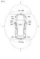
- FIG. 42 shows an example of the installation positions of the imaging unit 7410 and the outside-of-vehicle information detection unit 7420.
- the imaging units 7910, 7912, 7914, 7916, 7918 are provided at, for example, at least one of a front nose, a side mirror, a rear bumper, a back door, and an upper part of a windshield in the vehicle interior of the vehicle 7900.
- An imaging unit 7910 provided in the front nose and an imaging unit 7918 provided above the windshield in the vehicle cabin mainly acquire an image in front of the vehicle 7900.
- the imaging units 7912 and 7914 provided in the side mirror mainly acquire an image of the side of the vehicle 7900.
- An imaging unit 7916 provided in a rear bumper or a back door mainly acquires an image behind the vehicle 7900.
- the imaging unit 7918 provided above the windshield in the vehicle interior is mainly used for detecting a preceding vehicle, a pedestrian, an obstacle, a traffic light, a traffic sign, a lane, and the like.
- FIG. 42 shows an example of the imaging range of each of the imaging units 7910, 7912, 7914, and 7916.
- the imaging range a indicates the imaging range of the imaging unit 7910 provided on the front nose
- the imaging ranges b and c indicate the imaging ranges of the imaging units 7912 and 7914 provided on the side mirrors, respectively
- the imaging range d is 14 shows an imaging range of an imaging unit 7916 provided in a rear bumper or a back door.
- a bird's-eye view image of the vehicle 7900 viewed from above is obtained by superimposing image data captured by the imaging units 7910, 7912, 7914, and 7916.
- the external information detection units 7920, 7922, 7924, 7926, 7928, 7930 provided on the front, rear, side, corners of the vehicle 7900, and the upper part of the windshield in the passenger compartment may be, for example, an ultrasonic sensor or a radar device.
- the outside information detection units 7920, 7926, 7930 provided on the front nose, the rear bumper, the back door, and the windshield in the passenger compartment of the vehicle 7900 may be, for example, a LIDAR device.
- These outside-of-vehicle information detection units 7920 to 7930 are mainly used for detecting a preceding vehicle, a pedestrian, an obstacle, or the like.
- Out-of-vehicle information detection unit 7400 causes imaging section 7410 to capture an image of the outside of the vehicle, and receives data of the captured image. Further, the outside-of-vehicle information detection unit 7400 receives the detection information from the connected outside-of-vehicle information detection unit 7420.
- the out-of-vehicle information detection unit 7420 is an ultrasonic sensor, a radar device, or a LIDAR device
- the out-of-vehicle information detection unit 7400 transmits an ultrasonic wave, an electromagnetic wave, or the like, and receives information of a received reflected wave.
- the out-of-vehicle information detection unit 7400 may perform an object detection process or a distance detection process of a person, a vehicle, an obstacle, a sign, a character on a road surface, or the like based on the received information.
- the out-of-vehicle information detection unit 7400 may perform an environment recognition process for recognizing rainfall, fog, road surface conditions, and the like based on the received information.
- the outside-of-vehicle information detection unit 7400 may calculate the distance to an object outside the vehicle based on the received information.
- the outside-of-vehicle information detection unit 7400 may perform image recognition processing or distance detection processing for recognizing a person, a car, an obstacle, a sign, a character on a road surface, or the like based on the received image data.
- the out-of-vehicle information detection unit 7400 performs processing such as distortion correction or positioning on the received image data, and synthesizes image data captured by different imaging units 7410 to generate a bird's-eye view image or a panoramic image. Is also good.
- the outside-of-vehicle information detection unit 7400 may perform the viewpoint conversion process using image data captured by different imaging units 7410.
- the in-vehicle information detection unit 7500 detects information in the vehicle.
- a driver state detection unit 7510 that detects the state of the driver is connected.
- the driver state detection unit 7510 may include a camera that captures an image of the driver, a biological sensor that detects biological information of the driver, a microphone that collects sound in the vehicle compartment, and the like.
- the biological sensor is provided on, for example, a seat surface or a steering wheel, and detects biological information of a passenger sitting on a seat or a driver gripping the steering wheel.
- the in-vehicle information detection unit 7500 may calculate the degree of fatigue or concentration of the driver based on the detection information input from the driver state detection unit 7510, or determine whether the driver has fallen asleep. May be.
- the in-vehicle information detection unit 7500 may perform a process such as a noise canceling process on the collected audio signal.
- the integrated control unit 7600 controls the overall operation in the vehicle control system 7000 according to various programs.
- the input unit 7800 is connected to the integrated control unit 7600.
- the input unit 7800 is implemented by, for example, a device that can be input and operated by a passenger, such as a touch panel, a button, a microphone, a switch, or a lever. Data obtained by voice recognition of voice input by a microphone may be input to the integrated control unit 7600.
- the input unit 7800 may be, for example, a remote control device using infrared rays or other radio waves, or an external connection device such as a mobile phone or a PDA (Personal Digital Assistant) corresponding to the operation of the vehicle control system 7000. You may.
- Input unit 7800 may be, for example, a camera, in which case the occupant can input information by gesture. Alternatively, data obtained by detecting the movement of the wearable device worn by the passenger may be input. Further, the input unit 7800 may include, for example, an input control circuit that generates an input signal based on information input by a passenger or the like using the input unit 7800 and outputs the input signal to the integrated control unit 7600. By operating the input unit 7800, the passenger or the like inputs various data to the vehicle control system 7000 or instructs the vehicle control system 7000 to perform a processing operation.
- the storage unit 7690 may include a ROM (Read Only Memory) that stores various programs executed by the microcomputer and a RAM (Random Access Memory) that stores various parameters, calculation results, sensor values, and the like. Further, the storage unit 7690 may be realized by a magnetic storage device such as an HDD (Hard Disc Drive), a semiconductor storage device, an optical storage device, or a magneto-optical storage device.
- ROM Read Only Memory
- RAM Random Access Memory
- the general-purpose communication I / F 7620 is a general-purpose communication I / F that mediates communication with various devices existing in the external environment 7750.
- the general-purpose communication I / F 7620 is a cellular communication protocol such as GSM (registered trademark) (Global System of Mobile Communications), WiMAX, LTE (Long Term Evolution) or LTE-A (LTE-Advanced), or a wireless LAN (Wi-Fi). (Also referred to as (registered trademark)) and other wireless communication protocols such as Bluetooth (registered trademark).
- the general-purpose communication I / F 7620 connects to a device (for example, an application server or a control server) existing on an external network (for example, the Internet, a cloud network, or an operator-specific network) via a base station or an access point, for example. May be.
- the general-purpose communication I / F 7620 is a terminal (for example, a terminal of a driver, a pedestrian or a store, or a terminal of a MTC (Machine Type Communication)) existing near a vehicle using, for example, P2P (Peer To Peer) technology. May be connected.
- the dedicated communication I / F 7630 is a communication I / F that supports a communication protocol formulated for use in a vehicle.
- the dedicated communication I / F 7630 uses a standard protocol such as WAVE (Wireless Access in Vehicle Environment), which is a combination of lower layer IEEE 802.11p and upper layer IEEE 1609, DSRC (Dedicated Short Range Communications), or a cellular communication protocol. May be implemented.
- the dedicated communication I / F 7630 typically includes vehicle-to-vehicle communication, vehicle-to-infrastructure communication, vehicle-to-home communication (vehicle-to-home), and vehicle-to-vehicle (vehicle-to-pedestrian) communication. And) performing V2X communication, which is a concept including one or more of the communication.
- the positioning unit 7640 receives a GNSS signal from a GNSS (Global Navigation Satellite System) satellite (for example, a GPS signal from a GPS (Global Positioning System) satellite), executes positioning, and executes the latitude, longitude, and altitude of the vehicle. Generate location information including.
- positioning section 7640 may specify the current position by exchanging signals with a wireless access point, or may obtain position information from a terminal having a positioning function, such as a mobile phone, a PHS, or a smartphone.
- the beacon receiving unit 7650 receives, for example, radio waves or electromagnetic waves transmitted from a radio station or the like installed on a road, and acquires information such as the current position, traffic congestion, suspension of traffic, or required time.
- the function of beacon receiving section 7650 may be included in dedicated communication I / F 7630 described above.
- the in-vehicle device I / F 7660 is a communication interface that mediates a connection between the microcomputer 7610 and various in-vehicle devices 7760 existing in the vehicle.
- the in-vehicle device I / F 7660 may establish a wireless connection using a wireless communication protocol such as a wireless LAN, Bluetooth (registered trademark), NFC (Near Field Communication), or WUSB (Wireless USB).
- the in-vehicle device I / F 7660 is connected to a USB (Universal Serial Bus), an HDMI (registered trademark) (High-Definition Multimedia Interface), or an MHL (Mobile) via a connection terminal (and a cable if necessary) not shown.
- a wired connection such as High-definition (Link) may be established.
- the in-vehicle device 7760 may include, for example, at least one of a mobile device or a wearable device possessed by the occupant, and an information device carried or attached to the vehicle. Further, in-vehicle device 7760 may include a navigation device that searches for a route to an arbitrary destination. The in-vehicle device I / F 7660 exchanges control signals or data signals with these in-vehicle devices 7760.
- the in-vehicle network I / F 7680 is an interface that mediates communication between the microcomputer 7610 and the communication network 7010.
- the in-vehicle network I / F 7680 transmits and receives signals and the like according to a predetermined protocol supported by the communication network 7010.
- the microcomputer 7610 of the integrated control unit 7600 is connected to at least one of the general-purpose communication I / F 7620, the dedicated communication I / F 7630, the positioning unit 7640, the beacon receiving unit 7650, the in-vehicle device I / F 7660, and the in-vehicle network I / F 7680.
- the vehicle control system 7000 is controlled in accordance with various programs on the basis of the information acquired. For example, the microcomputer 7610 calculates a control target value of the driving force generation device, the steering mechanism, or the braking device based on the acquired information on the inside and outside of the vehicle, and outputs a control command to the driving system control unit 7100. Is also good.
- the microcomputer 7610 implements functions of an ADAS (Advanced Driver Assistance System) including a collision avoidance or a shock mitigation of a vehicle, a following operation based on a distance between vehicles, a vehicle speed maintaining operation, a vehicle collision warning, a vehicle lane departure warning, and the like. May be performed for the purpose of cooperative control.
- the microcomputer 7610 controls the driving force generation device, the steering mechanism, the braking device, and the like based on the acquired information about the surroundings of the vehicle, so that the vehicle automatically travels independently of the driver's operation. Cooperative control for driving or the like may be performed.
- the microcomputer 7610 is information obtained through at least one of the general-purpose communication I / F 7620, the dedicated communication I / F 7630, the positioning unit 7640, the beacon receiving unit 7650, the in-vehicle device I / F 7660, and the in-vehicle network I / F 7680. Based on the above, three-dimensional distance information between the vehicle and an object such as a nearby structure or a person may be generated, and local map information including surrounding information of the current position of the vehicle may be created. Further, the microcomputer 7610 may generate a warning signal by predicting a danger such as a collision of a vehicle, approach of a pedestrian or the like or entry into a closed road, based on the acquired information.
- the warning signal may be, for example, a signal for generating a warning sound or lighting a warning lamp.
- the sound image output unit 7670 transmits an output signal of at least one of a sound and an image to an output device capable of visually or audibly notifying a passenger of the vehicle or the outside of the vehicle of information.
- an audio speaker 7710, a display portion 7720, and an instrument panel 7730 are illustrated as output devices.
- the display unit 7720 may include, for example, at least one of an on-board display and a head-up display.
- the display portion 7720 may have an AR (Augmented Reality) display function.
- the output device may be another device such as a headphone, a wearable device such as a spectacle-type display worn by a passenger, a projector or a lamp other than these devices.
- the display device converts results obtained by various processes performed by the microcomputer 7610 or information received from other control units into various formats such as text, images, tables, and graphs. Display visually.
- the output device is a sound output device
- the sound output device converts an audio signal composed of reproduced sound data or acoustic data into an analog signal and outputs it audibly.
- At least two control units connected via the communication network 7010 may be integrated as one control unit.
- each control unit may be configured by a plurality of control units.
- the vehicle control system 7000 may include another control unit (not shown).
- some or all of the functions performed by one of the control units may be provided to another control unit. That is, if information is transmitted and received via the communication network 7010, the predetermined arithmetic processing may be performed by any of the control units.
- a sensor or device connected to any control unit may be connected to another control unit, and a plurality of control units may transmit and receive detection information to and from each other via the communication network 7010. .
- the technology according to the present disclosure can be applied to, for example, the imaging unit of the out-of-vehicle information detection unit among the configurations described above.
- a pixel array section in which pixels are arranged in a matrix, A plurality of vertical signal lines provided for each pixel column; And The plurality of vertical signal lines provided for each pixel column are arranged on a plurality of wiring layers stacked on the pixel, and are arranged so that orthogonal projections of the vertical signal lines on the plurality of wiring layers overlap.
- a connection portion for connecting a vertical signal line corresponding to the pixel to the pixel is provided in the wiring layer, The pixel signal is taken out of the vertical signal line via the connection, Imaging device.
- a via connected to the vertical signal line is provided as a connection portion, Pixel signals are extracted from vertical signal lines via vias.
- a relay line extending in a direction orthogonal to a direction in which the vertical signal line extends is arranged as a connection portion in each of the pixels as a connection part in a part of the plurality of stacked wiring layers. Pixel signals are extracted from the vertical signal lines via vias and relay lines.
- a relay line extending in a direction orthogonal to a direction in which the vertical signal line extends is arranged for each pixel in a state connected to the pixel as a connection portion. ing, The imaging device according to the above [A3].
- the trunk line is arranged so as to cross only the vertical signal line in a range that may be related to the connection, The imaging device according to the above [A4].
- [A6] In the wiring layer adjacent to the pixel among the plurality of stacked wiring layers, Further provided is a shield wiring arranged so as to cross only the vertical signal lines in a range that cannot be related to the connection, extending on the same line as the relay line, and applying a predetermined fixed voltage.
- [A7] The wiring layer on which the relay line is disposed is used for connecting a vertical signal line in one of the upper wiring layer and the lower wiring layer stacked adjacent to the wiring layer on which the relay line is disposed. Is provided as, The imaging device according to any one of the above [A3] to [A6].
- the wiring layer on which the relay line is disposed is provided for connection with the vertical signal line in the upper wiring layer and the lower wiring layer stacked adjacent to the wiring layer on which the relay line is disposed,
- the vertical signal lines in the upper wiring layer and the lower wiring layer are arranged so that the orthogonal projection of the vertical signal line to the wiring layer does not overlap.
- a connection portion for connecting a vertical signal line corresponding to the pixel to the pixel is provided in the wiring layer, The pixel signal is taken out of the vertical signal line via the connection, Having an image sensor configured as Imaging device.
- a via connected to the vertical signal line is provided as a connection portion, Pixel signals are extracted from vertical signal lines via vias.
- a relay line extending in a direction orthogonal to a direction in which the vertical signal line extends is arranged as a connection portion in each of the pixels as a connection part in a part of the plurality of stacked wiring layers. Pixel signals are extracted from the vertical signal lines via vias and relay lines.
- the trunk line is arranged so as to cross only the vertical signal line in a range that may be related to the connection, The imaging device according to [B4].
- a shield wiring arranged so as to cross only the vertical signal lines in a range that cannot be related to the connection, extending on the same line as the relay line, and applying a predetermined fixed voltage. The imaging device according to [B5].
- the wiring layer on which the relay line is disposed is used for connecting a vertical signal line in one of the upper wiring layer and the lower wiring layer stacked adjacent to the wiring layer on which the relay line is disposed. Is provided as, The imaging device according to any one of [B3] to [B6].
- the wiring layer on which the relay line is disposed is provided for connection with the vertical signal line in the upper wiring layer and the lower wiring layer stacked adjacent to the wiring layer on which the relay line is disposed, The imaging device according to any one of [B3] to [B6].
- the vertical signal lines in the upper wiring layer and the lower wiring layer are arranged so that the orthogonal projection of the vertical signal line to the wiring layer does not overlap. The imaging device according to [B8].
- a connection portion for connecting a vertical signal line corresponding to the pixel to the pixel is provided in the wiring layer, The pixel signal is taken out of the vertical signal line via the connection, Having an image sensor configured as Electronics.
- a via connected to the vertical signal line is provided as a connection portion, Pixel signals are extracted from vertical signal lines via vias.
- a relay line extending in a direction orthogonal to a direction in which the vertical signal line extends is arranged as a connection portion in each of the pixels as a connection part in a part of the plurality of stacked wiring layers. Pixel signals are extracted from the vertical signal lines via vias and relay lines.
- the trunk line is arranged so as to cross only the vertical signal line in a range that may be related to the connection, The electronic device according to the above [C4].
- a shield wiring arranged so as to cross only the vertical signal lines in a range that cannot be related to the connection, extending on the same line as the relay line, and applying a predetermined fixed voltage. The electronic device according to the above [C5].
- the wiring layer on which the relay line is disposed is used for connecting a vertical signal line in one of the upper wiring layer and the lower wiring layer stacked adjacent to the wiring layer on which the relay line is disposed. Is provided as, The electronic device according to any one of the above [C3] to [C6].
- the wiring layer on which the relay line is disposed is provided for connection with the vertical signal line in the upper wiring layer and the lower wiring layer stacked adjacent to the wiring layer on which the relay line is disposed, The electronic device according to any one of the above [C3] to [C6].
- the vertical signal lines in the upper wiring layer and the lower wiring layer are arranged so that the orthogonal projection of the vertical signal line to the wiring layer does not overlap. The electronic device according to the above [C8].
- SYMBOLS 1 ... Image sensor, 10 ... Pixel array part, 11 ... Pixel, 20 ... Vertical drive circuit, 30 ... Horizontal drive circuit, 40 ... Signal processing part, HSL ... Control Line, VSL: vertical signal line, WLA: wiring layer, VIA: via, BR: branch wiring, CL: relay line (first layer), MCL: relay line (2 Layer and after), DET ... vertical signal line detour
Landscapes
- Engineering & Computer Science (AREA)
- Multimedia (AREA)
- Signal Processing (AREA)
- Solid State Image Pick-Up Elements (AREA)
- Internal Circuitry In Semiconductor Integrated Circuit Devices (AREA)
Abstract
撮像素子は、画素が行列状に配列された画素アレイ部と、画素列単位で設けられた複数の垂直信号線とを含んでおり、画素列単位で設けられた複数の垂直信号線は、画素上に積層された複数の配線層に配置されていると共に、複数の配線層に対する垂直信号線の正射影が重なるように配置されており、配線層には、画素に対応する垂直信号線を画素に接続するための接続部が設けられており、画素の信号は、接続部を経由して垂直信号線から取り出される。
Description
本開示は、撮像素子、撮像装置、及び、電子機器に関する。
撮像機能を備えた電子機器にあっては、CMOS(Complementary Metal Oxide Semiconductor)センサなどの撮像素子を備えた撮像装置が使用されている。撮像素子は、フォトダイオード(Photo Diode:PD)などから成る光電変換部、光電変換された電荷が転送される浮遊拡散領域(Floating Diffusion region:FD)、及び、複数のトランジスタなどが組み合わされて成る画素を有している。そして、二次元マトリクス状に配置された複数の画素から出力される信号に基づいて画像が構築される。画素から出力される信号は、例えば、画素列ごとに配置された複数のA/D(Analog to Digital)変換器によって並列的にA/D変換され、デジタル信号として出力される。
近年、例えばハイエンドの表示装置にあっては120fpsといったフレームレートが一般的なものとなっている。また、スーパースロー機能を実現するため、撮像素子においても、960fpsなどといった高フレームレートでの撮像が可能なものが要求されている。高フレームレートで撮像を行うことで所謂フォーカルプレーン歪も低減されるので、高速に動く被写体を静止画として撮影することが求められるスポーツシーンの撮像においても、高フレームレートでの撮像の要求が高まっている。このため、画素からの信号を読み出すための垂直信号線を、各画素列に対して複数配置するといったことが行われている(例えば、特許文献1、非特許文献1を参照)。また、各画素列に多数の垂直信号線を配列するために、画素上に積層された複数の配線層のそれぞれに垂直信号線を配置するといったことも提案されている(例えば、非特許文献1を参照)。
A 1/1.7-inch 20Mpixel Back-illuminated stacked CMOS image sensor for new imaging applications, 2015 IEEE International Solid-State Circuits Conference - (ISSCC) Digest of Technical Papers
画素上に積層された複数の配線層のそれぞれに垂直信号線を配置するといった構成にあっては、通常、配線層に設けられたビア(Via)を介して、垂直信号線と画素とが接続される。デザインルールに従って垂直信号線やビアを配置するといった場合、各垂直信号線にビアを接続する必要があるため、複数の配線層において垂直信号線の正射影が重なるように配置するといったことはできない。しかしながら、垂直信号線の本数を増やして高フレームレート化を図るためには、複数の配線層において垂直信号線の正射影が重なるように配置されていても、垂直信号線と画素とを支障なく電気的に接続することができることが好ましい。
そこで、本開示は、複数の配線層において垂直信号線の正射影が重なるように配置されていても、垂直信号線と画素とを支障なく電気的に接続することができる撮像素子、係る撮像素子を備えた撮像装置、及び、係る撮像装置を備えた電子機器を提供することを目的とする。
上記の目的を達成するための本開示に係る撮像素子は、
画素が行列状に配列された画素アレイ部と、
画素列単位で設けられた複数の垂直信号線と、
を含んでおり、
画素列単位で設けられた複数の垂直信号線は、画素上に積層された複数の配線層に配置されていると共に、複数の配線層に対する垂直信号線の正射影が重なるように配置されており、
配線層には、画素に対応する垂直信号線を画素に接続するための接続部が設けられており、
画素の信号は、接続部を経由して垂直信号線から取り出される、
撮像素子である。
画素が行列状に配列された画素アレイ部と、
画素列単位で設けられた複数の垂直信号線と、
を含んでおり、
画素列単位で設けられた複数の垂直信号線は、画素上に積層された複数の配線層に配置されていると共に、複数の配線層に対する垂直信号線の正射影が重なるように配置されており、
配線層には、画素に対応する垂直信号線を画素に接続するための接続部が設けられており、
画素の信号は、接続部を経由して垂直信号線から取り出される、
撮像素子である。
上記の目的を達成するための本開示に係る撮像装置は、
画素が行列状に配列された画素アレイ部と、
画素列単位で設けられた複数の垂直信号線と、
を含んでおり、
画素列単位で設けられた複数の垂直信号線は、画素上に積層された複数の配線層に配置されていると共に、複数の配線層に対する垂直信号線の正射影が重なるように配置されており、
配線層には、画素に対応する垂直信号線を画素に接続するための接続部が設けられており、
画素の信号は、接続部を経由して垂直信号線から取り出される、
ように構成された撮像素子を有する、
撮像装置である。
画素が行列状に配列された画素アレイ部と、
画素列単位で設けられた複数の垂直信号線と、
を含んでおり、
画素列単位で設けられた複数の垂直信号線は、画素上に積層された複数の配線層に配置されていると共に、複数の配線層に対する垂直信号線の正射影が重なるように配置されており、
配線層には、画素に対応する垂直信号線を画素に接続するための接続部が設けられており、
画素の信号は、接続部を経由して垂直信号線から取り出される、
ように構成された撮像素子を有する、
撮像装置である。
上記の目的を達成するための本開示に係る電子機器は、
画素が行列状に配列された画素アレイ部と、
画素列単位で設けられた複数の垂直信号線と、
を含んでおり、
画素列単位で設けられた複数の垂直信号線は、画素上に積層された複数の配線層に配置されていると共に、複数の配線層に対する垂直信号線の正射影が重なるように配置されており、
配線層には、画素に対応する垂直信号線を画素に接続するための接続部が設けられており、
画素の信号は、接続部を経由して垂直信号線から取り出される、
ように構成された撮像素子を有する、
電子機器である。
画素が行列状に配列された画素アレイ部と、
画素列単位で設けられた複数の垂直信号線と、
を含んでおり、
画素列単位で設けられた複数の垂直信号線は、画素上に積層された複数の配線層に配置されていると共に、複数の配線層に対する垂直信号線の正射影が重なるように配置されており、
配線層には、画素に対応する垂直信号線を画素に接続するための接続部が設けられており、
画素の信号は、接続部を経由して垂直信号線から取り出される、
ように構成された撮像素子を有する、
電子機器である。
以下、図面を参照して、実施形態に基づいて本開示を説明する。本開示は実施形態に限定されるものではなく、実施形態における種々の数値や材料などは例示である。以下の説明において、同一要素または同一機能を有する要素には同一符号を用いることとし、重複する説明は省略する。尚、説明は、以下の順序で行う。
1.本開示に係る、撮像素子、撮像装置、及び、電子機器、全般に関する説明
2.第1の実施形態
3.第2の実施形態
4.第3の実施形態
5.第4の実施形態
6.第5の実施形態
7.第6の実施形態
8.応用例
9.本開示の構成
1.本開示に係る、撮像素子、撮像装置、及び、電子機器、全般に関する説明
2.第1の実施形態
3.第2の実施形態
4.第3の実施形態
5.第4の実施形態
6.第5の実施形態
7.第6の実施形態
8.応用例
9.本開示の構成
[本開示に係る、撮像素子、撮像装置、及び、電子機器、全般に関する説明]
本開示に係る撮像素子、本開示に係る撮像装置に用いられる撮像素子、並びに、本開示に係る電子機器に用いられる撮像素子(以下、これらを単に、本開示に係る撮像素子と呼ぶ場合がある)にあっては、
配線層には、接続部として、垂直信号線に接続されるビアが設けられており、
画素の信号は、ビアを経由して垂直信号線から取り出される、
構成とすることができる。
本開示に係る撮像素子、本開示に係る撮像装置に用いられる撮像素子、並びに、本開示に係る電子機器に用いられる撮像素子(以下、これらを単に、本開示に係る撮像素子と呼ぶ場合がある)にあっては、
配線層には、接続部として、垂直信号線に接続されるビアが設けられており、
画素の信号は、ビアを経由して垂直信号線から取り出される、
構成とすることができる。
上述した好ましい構成の本開示に係る撮像素子にあっては、
積層された複数の配線層のうちの一部の配線層には、接続部として、垂直信号線が延びる方向と直交する方向に延びる中継線が、画素ごとに配置されており、
画素の信号は、ビアと中継線とを経由して垂直信号線から取り出される、
構成とすることができる。
積層された複数の配線層のうちの一部の配線層には、接続部として、垂直信号線が延びる方向と直交する方向に延びる中継線が、画素ごとに配置されており、
画素の信号は、ビアと中継線とを経由して垂直信号線から取り出される、
構成とすることができる。
この場合において、
積層された複数の配線層のうち画素に隣接する配線層には、接続部として、垂直信号線が延びる方向と直交する方向に延びる中継線が、画素に接続された状態で画素ごとに配置されている、
構成とすることができる。
積層された複数の配線層のうち画素に隣接する配線層には、接続部として、垂直信号線が延びる方向と直交する方向に延びる中継線が、画素に接続された状態で画素ごとに配置されている、
構成とすることができる。
ここで、積層された複数の配線層のうち画素に隣接する配線層において、
中継線は、接続に関係し得る範囲の垂直信号線のみを横切るように配置されている、
構成とすることができる。更には、
接続に関係し得ない範囲の垂直信号線のみを横切るように配置された、中継線と同一線上に延在し、所定の固定電圧が印加されるシールド配線を更に備えている、
構成とすることができる。
中継線は、接続に関係し得る範囲の垂直信号線のみを横切るように配置されている、
構成とすることができる。更には、
接続に関係し得ない範囲の垂直信号線のみを横切るように配置された、中継線と同一線上に延在し、所定の固定電圧が印加されるシールド配線を更に備えている、
構成とすることができる。
あるいは又、上述した好ましい構成の本開示に係る撮像素子にあっては、
中継線が配置された配線層は、中継線が配置された配線層に隣接して積層された上層側の配線層および下層側の配線層のうち、一方の配線層における垂直信号線の接続用として設けられている、
構成とすることができる。
中継線が配置された配線層は、中継線が配置された配線層に隣接して積層された上層側の配線層および下層側の配線層のうち、一方の配線層における垂直信号線の接続用として設けられている、
構成とすることができる。
あるいは又、上述した好ましい構成の本開示に係る撮像素子にあっては、
中継線が配置された配線層は、中継線が配置された配線層に隣接して積層された上層側の配線層および下層側の配線層における垂直信号線との接続用として設けられている、
構成とすることができる。
中継線が配置された配線層は、中継線が配置された配線層に隣接して積層された上層側の配線層および下層側の配線層における垂直信号線との接続用として設けられている、
構成とすることができる。
この場合において、
上層側の配線層と下層側の配線層とにおける垂直信号線は、配線層に対する垂直信号線の正射影が重ならないように配置されている、
構成とすることができる。
上層側の配線層と下層側の配線層とにおける垂直信号線は、配線層に対する垂直信号線の正射影が重ならないように配置されている、
構成とすることができる。
あるいは又、本開示に係る撮像素子にあっては、
垂直信号線は、画素への接続に関与しないビアの部分を迂回するように配置されている、
構成とすることができる。
垂直信号線は、画素への接続に関与しないビアの部分を迂回するように配置されている、
構成とすることができる。
この場合において、
それぞれ隣接して積層された二つの配線層における垂直信号線は、配線層に対する垂直信号線の正射影が重ならないように配置されている、
構成とすることができる。
それぞれ隣接して積層された二つの配線層における垂直信号線は、配線層に対する垂直信号線の正射影が重ならないように配置されている、
構成とすることができる。
表面照射型の撮像素子は配線層側から光が入射する構成であるので、光路を確保するために各種配線の配置が制限されるといった問題があった。これに対し、裏面照射型の撮像素子にあっては、光路を確保するといった制限がない。従って、垂直信号線の本数を増やすといった観点からは、撮像素子を裏面照射型として構成することが好ましい。
配線層は、例えば、絶縁材料層を形成した後に開口などを適宜形成し、次いで、全面に導電材料を成膜した後に適宜パターニングを施すなどといった方法によって形成することができる。絶縁材料層は、例えば、SiOX系材料(シリコン系酸化膜を構成する材料)、SiN、SiON、SiOC、SiOF、SiCN、有機SOGを用いて形成することができる。また、導電材料として、例えば、銅、銅合金、アルミニウムを用いることができる。配線層は、各種化学的気相成長法や各種物理的気相成長法等の公知の方法と、リソグラフィ技術とエッチング技術との組合せや、リフトオフ法、メッキ法とダマシン法の組み合わせなどの公知の方法とを用いて構成することができる。
画素アレイ部は、例えばシリコンなどから成る半導体基板に形成することができる。画素は、光電変換部と光電変換部を駆動する各種回路から構成することができる。画素の構成は特に限定するものではなく、例えば、浮遊拡散領域蓄積型の構成であってもよいし、メモリ蓄積型の構成であってもよい。また、画素アレイ部を駆動するための各種回路は、画素アレイ部と一体であってもよいし、別体であってもよい。例えば、各種回路の一部が画素アレイ部と別体として構成されていてもよい。
また、本開示に係る撮像素子を備えた撮像装置として、デジタルスチルカメラやデジタルビデオカメラなどの撮像装置を例示することができる。また、本開示に係る撮像素子を備えた電子機器として、撮像機能を備えた携帯電話機、または、撮像機能を備えた他の機器といった各種の電子機器を例示することができる。
[第1の実施形態]
第1の実施形態は、本開示に係る、撮像素子、撮像装置、及び、電子機器に関する。
第1の実施形態は、本開示に係る、撮像素子、撮像装置、及び、電子機器に関する。
図1は、本開示が適用される撮像素子としてのCMOSイメージセンサの構成を説明するための模式図である。
図1に示すように、撮像素子1は、
画素11が行列状に配列された画素アレイ部10と、画素列単位で設けられた複数の垂直信号線VSLと、画素アレイ部10を駆動するための、垂直駆動回路20、水平駆動回路30、信号処理部40を備えている。これらの動作は、図示せぬ制御回路によって制御される。
画素11が行列状に配列された画素アレイ部10と、画素列単位で設けられた複数の垂直信号線VSLと、画素アレイ部10を駆動するための、垂直駆動回路20、水平駆動回路30、信号処理部40を備えている。これらの動作は、図示せぬ制御回路によって制御される。
後述する図6などを参照して後ほど詳しく説明するが、画素列単位で設けられた複数の垂直信号線VSLは、画素11上に積層された複数の配線層に配置されている。以下の説明において、最も画素側の1層目の配線層を符号WLA1、2層目の配線層を符号WLA2を用いて表す。3層目以降においても同様である。
画素アレイ部10は、光電変換部と光電変換された電荷が転送される浮遊拡散領域とを有する画素11がマトリクス状に配列されて成る。各画素11は、行ごとに、制御線HSLを介して垂直駆動回路20に接続される。また、各画素11は、列ごとに、垂直信号線VSLを介して、水平駆動回路30に接続される。
画素アレイ部10には、撮像対象からの光が入射する。画素11は、受光する光の光量に応じたレベルの画素信号を出力する。画素信号によって、被写体の画像が構成される。
画素11は、フォトダイオードなどから成る光電変換部、光電変換部からの電荷が転送される浮遊拡散領域、及び、画素11を駆動するためのトランジスタから構成される。例えば、これらの構成要素が、n型の半導体基板に設けられたp型ウェル内に形成されている構成とすることができる。
垂直駆動回路20は、画素アレイ部10の画素11を行ごとに順次駆動するための駆動信号を、制御線HSLを介して画素11に供給する。尚、図示の都合上、図1では画素行ごとに1本の制御線HSLを示した。実際には、後述する図2に示すように、1つの画素行に対応して、複数種類の制御線が配される。
また、画素11から出力される信号レベルやリセットレベルは、垂直信号線VSLを介して、水平駆動回路30に送られる。複数の垂直信号線VSLのそれぞれは、画素列を構成する画素11のうち、所定の関係にある画素群に対応して接続される。
水平駆動回路30は、画素11から出力される信号に基づいて2重サンプリング(Double Data Sampling:DDS)を施した後、A/D変換を行う。水平駆動回路30は、例えば、垂直信号線VSLごとに並列的にDDS処理を行う構成とすることができる。そして、水平駆動回路30から画素信号が信号処理部40に出力される。
信号処理部40は、例えば、水平駆動回路30からの画素信号に対して種々の信号処理を施し、画像出力として生成する。信号処理部40は、例えば、画素アレイ部10が形成される半導体基板に一体として形成されていてもよいし、別の基板に設けられていてもよい。更には、信号処理部40はDSPやソフトウェアによる処理であってもよい。
垂直駆動回路20は、シフトレジスタやアドレスデコーダなどの論理回路によって構成され、画素アレイ部10の各画素11を、全画素同時あるいは行単位で駆動する。例えば、画素11のリセット、露光、電荷の転送は全画素同時で行い、読み出しは行単位で行うように駆動するといった構成とすることができる。
図2は、撮像素子の画素の構成例を説明するための模式的な回路図である。
画素11は、
光電変換部PDに所定の電圧を印加するための初期化トランジスタ、
光電変換された電荷を浮遊拡散領域FDに転送するための転送トランジスタ、
浮遊拡散領域FDに所定の電圧を印加するためのリセットトランジスタ、
ゲート電極に浮遊拡散領域FDの電圧が印加される増幅トランジスタ、及び、
増幅トランジスタと垂直信号線VSLとを接続するための選択トランジスタ、
といった5つのトランジスタ(それぞれ、符号OFG,TRG,RST,AMP,SELで表す)、フォトダイオードから成る光電変換部PD、及び、浮遊拡散領域FDから構成されている。
光電変換部PDに所定の電圧を印加するための初期化トランジスタ、
光電変換された電荷を浮遊拡散領域FDに転送するための転送トランジスタ、
浮遊拡散領域FDに所定の電圧を印加するためのリセットトランジスタ、
ゲート電極に浮遊拡散領域FDの電圧が印加される増幅トランジスタ、及び、
増幅トランジスタと垂直信号線VSLとを接続するための選択トランジスタ、
といった5つのトランジスタ(それぞれ、符号OFG,TRG,RST,AMP,SELで表す)、フォトダイオードから成る光電変換部PD、及び、浮遊拡散領域FDから構成されている。
光電変換部PDの一端(アノード側)、及び、浮遊拡散領域FDの一端には、一定の電圧(例えば接地電圧)が供給される。駆動電圧が供給される電源線と光電変換部PDの他端(カソード側)とは、初期化トランジスタOFGを介して接続されている。駆動電圧が供給される電源線と浮遊拡散領域FDの他端とは、リセットトランジスタRSTを介して接続されている。光電変換部PDの他端と浮遊拡散領域FDの他端とは、転送トランジスタTRGを介して接続されている。
増幅トランジスタAMPの一端は駆動電圧が供給される電源線に接続されている。増幅トランジスタAMPの他端と垂直信号線VSLとは、選択トランジスタSELを介して接続されている。増幅トランジスタAMPのゲート電極は、浮遊拡散領域FDの他端に接続されている。
画素11の基本的な動作について説明する。尚、ここでは、トランジスタOFG,TRG,RST,SELのゲート電極に接続される制御線を、それぞれ、制御線HSL(OFG)、制御線HSL(TRG)、制御線HSL(RST)、制御線HSL(SEL)と表記する。
先ず、全行の制御線HSL(OFG)がハイレベルとされている状態(換言すれば、初期化トランジスタOFGを介して電圧VDDが印加され光電変換部PDがリセットされている状態)から、全行の制御線HSL(OFG)を一括してローレベルとする。これによって、全画素において露光が開始される。
そして、所定の露光期間が経過した後、全行の制御線HSL(TRG)を所定の期間ハイレベルとする。これによって、転送トランジスタTRGが導通状態となって、光電変換された電荷が浮遊拡散領域FDに転送され、保持される。
次いで、画素信号を読み出す。具体的には、読み出し対象となる行の制御線HSL(SEL)を、所定の期間ハイレベルとする。これによって、増幅トランジスタAMPは導通状態の選択トランジスタSELを介して垂直信号線VSLに接続される。そして、その期間内に、制御線HSL(RST)を一定期間ハイレベルとする。この動作によって、信号レベルとリセットレベルの読出しが行われる。
垂直信号線VSLを介して読み出される信号レベル、リセットレベルは、それぞれ、増幅トランジスタAMPのゲート電圧によって制御される。水平駆動回路30は、リセットレベルと信号レベルとの差分を求め、それを映像信号VOUTとする。
以上、画素11の基本的な動作について説明した。尚、上述した画素の構成は一例であって、例えばOFGが省略されている構成やトランジスタSELを複数備える構成など種々の構成をとり得る。
次いで、本開示の理解を助けるため、図3、図4、及び、図5を参照して参考例の配線層の構造について説明する。
図3は、参考例の配線層における各種配線の構造を説明するための模式的な斜視図である。図4は、参考例の配線層における各層の構造を説明するための模式的な斜視図である。図5は、参考例の配線層における積層状態の正射影と各層の構造との関係を説明するための模式的な平面図である。尚、各種配線などの位置関係を明瞭にするため、これらの図においては、配線層を構成する絶縁材料の図示を省略した。後述する他の図面においても同様である。
図3に示す例では、1つの画素列に対して、4本の垂直信号線VSLが配置されている。図4に示すように、4本の垂直信号線VSLのうち2本は2層目の配線層WLA2に配置されており、残りの2本は3層目の配線層WLA3に配置されている。最も画素側に位置する1層目の配線層WLA1には、各画素11に対応して設けられた、画素11に接続された中継線CLが配置されている。符号VIAは、配線層に設けられた接続用のビアを示す。
図3に示すように、垂直信号線VSLと中継線CLとは、ビアによって接続される。垂直信号線VSLと中継線CLとの間に他の配線層を含む場合には、当該配線層に設けられたビアも経由して接続される。
図5に示すように、2層目の垂直信号線VSLと3層目の垂直信号線VSLとは、正射影が重ならないように配置されている。この場合において、更に4層目の配線層を形成して垂直信号線VSLを増やそうとする場合、正射影が重なるように垂直信号線VSLを配置することはできない。なぜなら、4層目の垂直信号線VSLにもビアを接続する必要があるが、下層の垂直信号線VSLと電気的に独立した状態でビアを配置することができないためである。また、各種配線などの製造にあたっては、製造上必要とされる最小線幅と最小スペースを確保する必要がある。図5に示す例では、2層目の垂直信号線VSLとビアの間は最小スペース(符号MPで表す)を確保するように配置されている。従って、隣接する垂直信号線VSLの間に更に垂直信号線VSLを配置するといったこともできない。
以上、参考例の配線層の構造について説明した。次いで、図を参照して、第1の実施形態に係る撮像素子に用いられる配線層の構造について説明する。
図6は、第1の実施形態に係る撮像素子に用いられる配線層における各種配線の構造を説明するための模式的な斜視図である。図7は、配線層における各層の構造を説明するための模式的な斜視図である。図8は、配線層における積層状態の正射影と各層の構造との関係を説明するための模式的な平面図である。
第1の実施形態に係る撮像素子に用いられる配線層にあっては、画素列単位で設けられた複数の垂直信号線VSLは、画素11上に積層された複数の配線層に配置されている。図に示す例では、配線層は2層構成(WLA1,WLA2)であって、各層に2本の垂直信号線VSLが配置されている。
配線層には、接続部として、垂直信号線VSLに接続されるビアが設けられており、画素11の信号は、ビアを経由して垂直信号線VSLから取り出される。配線層に設けられた接続部を構成するビアは、2本の垂直信号線VSLの間に配置されている。垂直信号線VSLと配線層に設けられたビアとは、垂直信号線VSLが伸びる方向と直交する方向に伸びる枝配線BRによって接続されている。2層目の垂直信号線VSLに接続されたビアに対応して、1層目の配線層WLA1にもビアが形成されている。
第1の実施形態にあっては、1層目に中継線を設けることなく、垂直信号線VSLと画素11とを接続することができる。そして、図8に示すように、複数の配線層に対する垂直信号線VSLの正射影が重なるように配置することができる。
図9、図10、及び、図11を参照して、垂直信号線VSLと画素11との接続関係について説明する。
図9は、2層目の垂直信号線と画素との接続関係を説明するための模式的な斜視図である。図10Aは、垂直信号線VSL21と画素との接続関係を説明するための模式的な端面図である。図10Bは、垂直信号線VSL22と画素との接続関係を説明するための模式的な端面図である。尚、図において、1層目のビアを符号VIA(1)で示し、2層目のビアを符号VIA(2)で示す。
図9と図10に示すように、2層目の垂直信号線VSLは、2層目の枝配線BRと、1層目と2層目とに設けられたビアによって、対応する画素11に接続される。
図11Aは、垂直信号線VSL11と画素との接続関係を説明するための模式的な端面図である。図11Bは、垂直信号線VSL12と画素との接続関係を説明するための模式的な端面図である。
図11に示すように、1層目の垂直信号線VSLは、1層目の枝配線BRと、1層目に設けられたビアによって、対応する画素11に接続される。
以上説明したように、第1の実施形態にあっては、複数の配線層に対する垂直信号線VSLの正射影が重なるように配置することができる。更には、1層目に中継線を設けることなく、垂直信号線VSLと画素11とを接続することができる。
尚、ビアの配置の均一化などといった観点から、1層目の垂直信号線VSLの接続のために1層目に設けられたビアに対応して、2層目にもビアを設けるといった態様も考えられる。図12は、そのような第1変形例に係る配線層における積層状態の正射影と各層の構造との関係を説明するための模式的な平面図である。図13Aは、垂直信号線VSL11と画素との接続関係を説明するための模式的な端面図である。図13Bは、垂直信号線VSL12と画素との接続関係を説明するための模式的な端面図である。
第1の実施形態にあっては、積層する配線層の数を増やすことによって、制限なく垂直信号線を増やすことができる。以下、配線層を3層構成とした第2変形例について説明する。
図14は、第2変形例に係る配線層における各層の構造を説明するための模式的な斜視図である。図15は、配線層における各層の構造を説明するための模式的な斜視図である。図16は、配線層における積層状態の正射影と各層の構造との関係を説明するための模式的な平面図である。
第2変形例は、図6ないし図8を参照して説明した構成に対して、更に、3層目の垂直信号線VSL31,VSL32などを加えたといった構成である。
図17は、第2変形例に係る3層目の配線層における垂直信号線と画素との接続関係を説明するための模式的な斜視図である。図18は、垂直信号線VSL31と画素との接続関係を説明するための模式的な端面図である。図19は、垂直信号線VSL32と画素との接続関係を説明するための模式的な端面図である。
図17ないし図19に示すように、3層目の垂直信号線VSLは、3層目の枝配線BRと、1層目と2層目と3層目とに設けられたビアによって、対応する画素11に接続される。2層目と3層目の垂直信号線VSLと画素11との接続関係は、図9ないし図12を参照して説明した接続関係と同様であるので、説明を省略する。
以上、第2変形例について説明した。
図6ないし図19に示した構成において、配線層に設けられた接続部を構成するビアは、2本の垂直信号線VSLの間に配置されている。従って、ビアが画素11に接続される位置は、画素11を問わず一定である。
各画素11の画素回路の構成が一定である場合、垂直信号線VSLと接続される選択トランジスタが画素11において占める位置も一定である。従って、ビアが画素11に接続される位置は、画素11を問わず一定であることが好ましい。図6ないし図19に示した構成は、このような用途に適している。
一方、場合によっては、1つの浮遊拡散領域FDを2つの画素で共有するなどといった構成も考えられる。このような共有画素列構成の場合、画素回路の構成が画素ごとに交互に変わる。従って、ビアが画素に接続される位置は、画素ごとに交互に変わるといった構成とすることが好ましい。このような用途に適した第3変形例について説明する。
図20は、第3変形例に係る配線層における積層状態の正射影と各層の構造との関係を説明するための模式的な平面図である。
図に示すように、第3変形例において、ビアは2本の垂直信号線VSLの外側に配置されている。また、ビアが画素11に接続される位置は、画素11ごとに交互に配列されている。ビアと垂直信号線VSLとは枝配線BRによって接続されている。
第3変形例においても、1層目の垂直信号線VSLは1層目の枝配線BRと1層目に設けられたビアによって対応する画素11に接続される。2層目の垂直信号線VSLは2層目の枝配線BRと1層目と2層目とに設けられたビアによって対応する画素11に接続される。3層目の垂直信号線VSLは3層目の枝配線BRと1層目と2層目と3層目とに設けられたビアによって対応する画素11に接続される。
上述した各種変形例を含む第1の実施形態にあっては、各層の垂直信号線の本数は基本的には2本に限定される。デザインルールの最小ピッチで各層に配置できる最大配線本数に対して、配線層の総数と垂直信号線の総本数の関係を図21に示す。
[第2の実施形態]
第2の実施形態も、本開示に係る、撮像素子、撮像装置、及び、電子機器に関する。
第2の実施形態も、本開示に係る、撮像素子、撮像装置、及び、電子機器に関する。
第1の実施形態にあっては、配線層に配置する垂直信号線の本数に制限があった。第2の実施形態にあっては、配線層に3本以上の垂直信号線を配置することができる。
以下、図を参照して、第2の実施形態に係る撮像素子に用いられる配線層の構造について説明する。尚、第2の実施形態に係る撮像素子の構成例は、図1に示した構成例と同様であるので、説明を省略する。
図22は、第2の実施形態に係る撮像素子に用いられる配線層における垂直信号線と画素との接続関係を説明するための模式的な斜視図である。図23は、配線層における各層の構造を説明するための模式的な斜視図である。図24は、配線層における積層状態の正射影と各層の構造との関係を説明するための模式的な平面図である。
第2の実施形態に係る撮像素子に用いられる配線層においても、画素列単位で設けられた複数の垂直信号線VSLは、画素11上に積層された複数の配線層に配置されている。図に示す例では、配線層は5層構成であって、2層目WLA2、3層目WLA3、及び、5層目WLA5のそれぞれに、3本の垂直信号線VSLが配置されている。図24に示すように、複数の配線層に対する垂直信号線VSLの正射影は、すべて重なるように配置されている。
配線層には、接続部として、垂直信号線VSLに接続されるビアが設けられている。これに加えて、第2の実施形態にあっては、積層された複数の配線層のうちの一部の配線層(図に示す例では4層目と1層目)には、接続部として、垂直信号線VSLが延びる方向と直交する方向に延びる中継線が、画素11ごとに配置されている。特に、積層された複数の配線層のうち画素11に隣接する1層目の配線層WLA1には、接続部として、垂直信号線VSLが延びる方向と直交する方向に延びる中継線が、画素11に接続された状態で画素11ごとに配置されている。
表記の都合上、1層目の配線層WLA1に設けられた中継線を符号CLで表し、それ以外の配線層に設けられた中継線を符号MCLで表す。後述する他の実施形態においても同様である。
次いで、垂直信号線VSLと画素11との接続関係について説明する。
図25は、図22において示された垂直信号線VSL31と画素との接続関係を説明するための模式的な端面図である。
図に示すように、5層目の垂直信号線VSL31は、5層目に設けられたビアを介して4層目に設けられた中継線MCLの一端に接続される。そして、中継線MCLの他端は、4層目と3層目と2層目とに設けられたビアを介して1層目の中継線CLに接続される。このように、5層目の垂直信号線VSL31は、ビアと中継線とを介して、対応する画素11に接続される。5層目の他の垂直信号線VSL32,VSL33についても同様である。
図26は、配線層における垂直信号線と画素との接続関係を説明するための模式的な斜視図である。図27は、図26において示された垂直信号線VSL21と画素との接続関係を説明するための模式的な端面図である。
図に示すように、3層目の垂直信号線VSL21は、4層目に設けられたビアを介して4層目に設けられた中継線MCLの一端に接続される。そして、中継線MCLの他端は、4層目と3層目と2層目とに設けられたビアを介して1層目の中継線CLに接続される。このように、3層目の垂直信号線VSL21は、ビアと中継線とを介して、対応する画素11に接続される。3層目の他の垂直信号線VSL22,VSL23についても同様である。
以上説明したように、中継線MCLが配置された4層目の配線層WLA4は、中継線MCLが配置された配線層に隣接して積層された上層側(即ち5層目)の配線層WLA5および下層側(即ち3層目)の配線層WLA3における垂直信号線との接続用として設けられている。なお、場合によっては、中継線が配置された配線層は、中継線が配置された配線層に隣接して積層された上層側の配線層および下層側の配線層のうち、一方の配線層における垂直信号線の接続用として設けられている構成とすることもできる。
図28は、配線層における垂直信号線と画素との接続関係を説明するための模式的な斜視図である。図29は、図28において示された垂直信号線VSL11と画素との接続関係を説明するための模式的な端面図である。
図に示すように、2層目の垂直信号線VSL11は、2層目に設けられたビアを介して1層目の中継線CLに接続される。このように、2層目の垂直信号線VSL11は、ビアと中継線とを介して、対応する画素11に接続される。3層目の他の垂直信号線VSL12,VSL13についても同様である。
第2の実施形態にあっては、一部の配線層に中継線を設けることが必要となるが、1つの配線層に2本以上の垂直信号線を配置することができる。デザインルールの最小ピッチで各層に配置できる最大配線本数に対して、配線層の総数と垂直信号線の総本数の関係を図30に示す。
[第3の実施形態]
第3の実施形態も、本開示に係る、撮像素子、撮像装置、及び、電子機器に関する。
第3の実施形態も、本開示に係る、撮像素子、撮像装置、及び、電子機器に関する。
第2の実施形態において図22ないし図24に示す例では、垂直信号線が設けられている2層目、3層目、及び、5層目のすべてにおいて、垂直信号線の正射影が重なるように配置されている。
しかしながら、場合によっては、中継線が設けられた配線層の上層側の配線層と下層側の配線層とにおける垂直信号線については正射影が重ならないように配置することによって、配線間に生ずる容量を小さくするといった構成も考えられる。
以下、図を参照して、第3の実施形態に係る撮像素子に用いられる配線層の構造について説明する。尚、第3の実施形態に係る撮像素子の構成例も、図1に示した構成例と同様であるので、説明を省略する。
図31は、第3の実施形態に係る撮像素子に用いられる配線層における垂直信号線と画素との接続関係を説明するための模式的な斜視図である。図32は、配線層における各層の構造を説明するための模式的な端面図である。
第3の実施形態に係る撮像素子に用いられる配線層においても、画素列単位で設けられた複数の垂直信号線VSLは、画素11上に積層された複数の配線層に配置されている。図に示す例では、配線層は7層構成であって、2層目、4層目、5層目、及び、7層目のそれぞれに、垂直信号線VSLが配置されている。
配線層には、接続部として、垂直信号線VSLに接続されるビアが設けられている。これに加えて、第3の実施形態にあっては、積層された複数の配線層のうちの一部の配線層(図に示す例では6層目WLA6と3層目WLA3と1層目WLA1)には、接続部として、垂直信号線VSLが延びる方向と直交する方向に延びる中継線が、画素11ごとに配置されている。特に、積層された複数の配線層のうち画素11に隣接する1層目の配線層には、接続部として、垂直信号線VSLが延びる方向と直交する方向に延びる中継線が、画素11に接続された状態で画素11ごとに配置されている。
中継線が配置された6層目と3層目の配線層は、中継線が配置された配線層に隣接して積層された上層側の配線層および下層側の配線層における垂直信号線VSLとの接続用として設けられている。そして、上層側の配線層と下層側の配線層とにおける垂直信号線VSLは、配線層に対する垂直信号線VSLの正射影が重ならないように配置されている。
そして、2層目と5層目とに設けられた垂直信号線VSLは、正射影が重なるように配置されている。また、4層目と7層目とに設けられた垂直信号線VSLは、正射影が重なるように配置されている。このように、第3の実施形態にあっては、配線層の垂直信号線を正射影が重なるように配置でき、且つ、配線間に生ずる容量を小さくすることができる。
[第4の実施形態]
第4の実施形態も、本開示に係る、撮像素子、撮像装置、及び、電子機器に関する。
第4の実施形態も、本開示に係る、撮像素子、撮像装置、及び、電子機器に関する。
第2の実施形態や第3の実施形態にあっては、複数の配線層に中継線を設ける必要がある。しかしながら、配線層に配置される垂直信号線の間隔に余裕がある場合、ビアを避けるように配線を迂回することによって、中継線を設ける配線層の数を削減するといったことができる。
図33は、第4の実施形態に係る撮像素子に用いられる配線層における垂直信号線と画素との接続関係を説明するための模式的な斜視図である。図34は、配線層における積層状態の正射影と各層の構造との関係を説明するための模式的な平面図である。
第4の実施形態に係る撮像素子に用いられる配線層においても、画素列単位で設けられた複数の垂直信号線VSLは、画素11上に積層された複数の配線層に配置されている。図に示す例では、配線層は3層構成であって、2層目WLA2と3層目WLA3のそれぞれに、垂直信号線VSLが配置されている。図34に示すように、複数の配線層に対する垂直信号線VSLの正射影は重なるように配置されている。
配線層には、接続部として、垂直信号線VSLに接続されるビアが設けられている。これに加えて、第4の実施形態にあっては、積層された複数の配線層のうち画素11に隣接する1層目の配線層には、接続部として、垂直信号線VSLが延びる方向と直交する方向に延びる中継線CLが、画素11に接続された状態で画素11ごとに配置されている。
図に示すように、3層目の垂直信号線VSL21は、3層目と4層目とに設けられたビアを介して1層目の中継線CLに接続される。このように、3層目の垂直信号線VSL21は、ビアと中継線とを介して、対応する画素11に接続される。3層目の他の垂直信号線VSL22についても同様である。
3層目の垂直信号線VSL21の接続に関与する2層目のビアは、2層目の垂直信号線VSL11と画素11への接続には関与しない。同様に、3層目の垂直信号線VSL22の接続に関与する2層目のビアは、2層目の垂直信号線VSL12と画素11への接続には関与しない。従って、図5に示すように、垂直信号線VSL11,VSL12は、画素11への接続に関与しないビアの部分を迂回するように配置されている。符号DETは、垂直信号線VSLの迂回部を示す。
以上、配線層が3層構成の例について説明したが、第4の実施形態にあっては、積層する配線層の数を増やすことによって、制限なく垂直信号線を増やすことができる。また、場合によっては、隣接する配線層とでは垂直信号線の正射影が重ならないようにすることによって容量の低減を図るといった構成とすることもできる。
第4の実施形態にあっては、垂直信号線に迂回部を設けることが必要となるが、中継線を設ける配線層の数を削減するといったことができる。デザインルールの最小ピッチで各層に配置できる最大配線本数に対して、配線層の総数と垂直信号線の総本数の関係を図35に示す。
[第5の実施形態]
第5の実施形態も、本開示に係る、撮像素子、撮像装置、及び、電子機器に関する。
第5の実施形態も、本開示に係る、撮像素子、撮像装置、及び、電子機器に関する。
上述した第1の実施形態から第4の実施形態を適宜組み合わせるといったことも可能である。第5の実施形態として、第1の実施形態と第2の実施形態とを組み合わせた形態について説明する。
図36は、第5の実施形態に係る撮像素子に用いられる配線層における垂直信号線と画素との接続関係を説明するための模式的な斜視図である。図37は、図36において示された垂直走査線VSL21と画素との接続関係を説明するための模式的な端面図である。
第5の実施形態に係る撮像素子に用いられる配線層においても、画素列単位で設けられた複数の垂直信号線VSLは、画素11上に積層された複数の配線層に配置されている。図に示す例では、配線層は3層構成であって、2層目WLA2と3層目WLA3のそれぞれに、垂直信号線VSLが配置されている。また、配線層に対する垂直信号線VSLの正射影は重なるように配置されている。
配線層には、接続部として、垂直信号線VSLに接続されるビアが設けられている。これに加えて、第5の実施形態にあっては、積層された複数の配線層のうち画素11に隣接する1層目の配線層には、接続部として、垂直信号線VSLが延びる方向と直交する方向に延びる中継線CLが、画素11に接続された状態で画素11ごとに配置されている。
図に示すように、3層目の垂直信号線VSL21は、3層目の枝配線BRと、2層目と3層目とに設けられたビアによって、中継線CLに接続される。3層目の他の垂直信号線VSL22,VSL23,VSL24についても同様である。
尚、図は省略するが、2層目の垂直信号線VSL11,VSL12,VSL13,VSL14は、2層目の枝配線BRと、2層目とに設けられたビアによって、中継線CLに接続される。
第5の実施形態にあっては、配線層に配置する垂直信号線の数を増やすことができ、また、中継線を設ける配線層の数を削減するといったことができる。デザインルールの最小ピッチで各層に配置できる最大配線本数に対して、配線層の総数と垂直信号線の総本数の関係を図38に示す。
[第6の実施形態]
第6の実施形態も、本開示に係る、撮像素子、撮像装置、及び、電子機器に関する。
第6の実施形態も、本開示に係る、撮像素子、撮像装置、及び、電子機器に関する。
第2の実施形態ないし第5の実施形態にあっては、画素に隣接する1層目の配線層に、垂直信号線が延びる方向と直交する方向に延びる中継線CLが、画素に接続された状態で画素ごとに配置されていた。
これらの例において、中継線CLは、複数の垂直信号線全てを横切るような長さで配置されていた。しかしながら、この構成では、中継線CLと垂直信号線VSLとの間の寄生容量が大きくなり、画素信号のセトリング時間を長くする要因となり得る。
そこで、第6の実施形態にあっては、積層された複数の配線層のうち画素に隣接する配線層において、中継線は、接続に関係し得る範囲の垂直信号線VSLのみを横切るように配置されている構成とした。更に、接続に関係し得ない範囲の垂直信号線VSLのみを横切るように配置された、中継線と同一線上に延在し、所定の固定電圧が印加されるシールド配線を更に備えている構成とした。シールド配線を設けることによって、ノイズの抑制効果も高めることができる。
ここでは、第5の実施形態の変形例として、第6の実施形態を説明する。
図39は、第6の実施形態に係る撮像素子に用いられる配線層における垂直信号線と画素との接続関係を説明するための模式的な斜視図である。図40は、図39に引き続き、配線層における垂直信号線と画素との接続関係を説明するための模式的な斜視図である。
図39は、図37において示す垂直信号線VSL11,VSL12,VSL21,VSL22が接続され得る範囲の接続関係を示している。中継線CLは、上述した4本の垂直信号線のみを横切るように配置されている。上述した4本の信号線が順次画素11に接続されるとすれば、連続する4つの画素11において中継線CLの形状は同じとなる。符号SLDは、中継線CLと同一線上に延在し、所定の固定電圧が印加されるシールド配線を示す。
また、図40は、図37において示す垂直信号線VSL13,VSL14,VSL23,VSL24が接続され得る範囲の接続関係を示している。中継線CLは、上述した4本の垂直信号線のみを横切るように配置されている。上述した4本の信号線が順次画素11に接続されるとすれば、連続する4つの画素11において中継線CLの形状は同じとなる。符号SLDは、中継線CLと同一線上に延在し、所定の固定電圧が印加されるシールド配線を示す。
以上、本開示を好ましい実施形態に基づき説明したが、本開示はこれらの実施形態に限定されるものではない。上記の各実施形態において説明した撮像素子の構成、構造は例示であり、適宜、変更することができる。
本開示によれば、複数の配線層において垂直信号線の正射影が重なるように配置されていても、垂直信号線と画素とを支障なく電気的に接続することができる。従って、垂直信号線を効率的に増やすことができるので、撮像素子の高フレームレート化を図ることができる。
[応用例]
本開示に係る技術は、様々な製品へ応用することができる。例えば、本開示に係る技術は、自動車、電気自動車、ハイブリッド電気自動車、自動二輪車、自転車、パーソナルモビリティ、飛行機、ドローン、船舶、ロボット、建設機械、農業機械(トラクター)などのいずれかの種類の移動体に搭載される装置として実現されてもよい。
本開示に係る技術は、様々な製品へ応用することができる。例えば、本開示に係る技術は、自動車、電気自動車、ハイブリッド電気自動車、自動二輪車、自転車、パーソナルモビリティ、飛行機、ドローン、船舶、ロボット、建設機械、農業機械(トラクター)などのいずれかの種類の移動体に搭載される装置として実現されてもよい。
図41は、本開示に係る技術が適用され得る移動体制御システムの一例である車両制御システム7000の概略的な構成例を示すブロック図である。車両制御システム7000は、通信ネットワーク7010を介して接続された複数の電子制御ユニットを備える。図41に示した例では、車両制御システム7000は、駆動系制御ユニット7100、ボディ系制御ユニット7200、バッテリ制御ユニット7300、車外情報検出ユニット7400、車内情報検出ユニット7500、及び統合制御ユニット7600を備える。これらの複数の制御ユニットを接続する通信ネットワーク7010は、例えば、CAN(Controller Area Network)、LIN(Local Interconnect Network)、LAN(Local Area Network)又はFlexRay(登録商標)等の任意の規格に準拠した車載通信ネットワークであってよい。
各制御ユニットは、各種プログラムにしたがって演算処理を行うマイクロコンピュータと、マイクロコンピュータにより実行されるプログラム又は各種演算に用いられるパラメータ等を記憶する記憶部と、各種制御対象の装置を駆動する駆動回路とを備える。各制御ユニットは、通信ネットワーク7010を介して他の制御ユニットとの間で通信を行うためのネットワークI/Fを備えるとともに、車内外の装置又はセンサ等との間で、有線通信又は無線通信により通信を行うための通信I/Fを備える。図41では、統合制御ユニット7600の機能構成として、マイクロコンピュータ7610、汎用通信I/F7620、専用通信I/F7630、測位部7640、ビーコン受信部7650、車内機器I/F7660、音声画像出力部7670、車載ネットワークI/F7680及び記憶部7690が図示されている。他の制御ユニットも同様に、マイクロコンピュータ、通信I/F及び記憶部等を備える。
駆動系制御ユニット7100は、各種プログラムにしたがって車両の駆動系に関連する装置の動作を制御する。例えば、駆動系制御ユニット7100は、内燃機関又は駆動用モータ等の車両の駆動力を発生させるための駆動力発生装置、駆動力を車輪に伝達するための駆動力伝達機構、車両の舵角を調節するステアリング機構、及び、車両の制動力を発生させる制動装置等の制御装置として機能する。駆動系制御ユニット7100は、ABS(Antilock Brake System)又はESC(Electronic Stability Control)等の制御装置としての機能を有してもよい。
駆動系制御ユニット7100には、車両状態検出部7110が接続される。車両状態検出部7110には、例えば、車体の軸回転運動の角速度を検出するジャイロセンサ、車両の加速度を検出する加速度センサ、あるいは、アクセルペダルの操作量、ブレーキペダルの操作量、ステアリングホイールの操舵角、エンジン回転数又は車輪の回転速度等を検出するためのセンサのうちの少なくとも一つが含まれる。駆動系制御ユニット7100は、車両状態検出部7110から入力される信号を用いて演算処理を行い、内燃機関、駆動用モータ、電動パワーステアリング装置又はブレーキ装置等を制御する。
ボディ系制御ユニット7200は、各種プログラムにしたがって車体に装備された各種装置の動作を制御する。例えば、ボディ系制御ユニット7200は、キーレスエントリシステム、スマートキーシステム、パワーウィンドウ装置、あるいは、ヘッドランプ、バックランプ、ブレーキランプ、ウィンカー又はフォグランプ等の各種ランプの制御装置として機能する。この場合、ボディ系制御ユニット7200には、鍵を代替する携帯機から発信される電波又は各種スイッチの信号が入力され得る。ボディ系制御ユニット7200は、これらの電波又は信号の入力を受け付け、車両のドアロック装置、パワーウィンドウ装置、ランプ等を制御する。
バッテリ制御ユニット7300は、各種プログラムにしたがって駆動用モータの電力供給源である二次電池7310を制御する。例えば、バッテリ制御ユニット7300には、二次電池7310を備えたバッテリ装置から、バッテリ温度、バッテリ出力電圧又はバッテリの残存容量等の情報が入力される。バッテリ制御ユニット7300は、これらの信号を用いて演算処理を行い、二次電池7310の温度調節制御又はバッテリ装置に備えられた冷却装置等の制御を行う。
車外情報検出ユニット7400は、車両制御システム7000を搭載した車両の外部の情報を検出する。例えば、車外情報検出ユニット7400には、撮像部7410及び車外情報検出部7420のうちの少なくとも一方が接続される。撮像部7410には、ToF(Time Of Flight)カメラ、ステレオカメラ、単眼カメラ、赤外線カメラ及びその他のカメラのうちの少なくとも一つが含まれる。車外情報検出部7420には、例えば、現在の天候又は気象を検出するための環境センサ、あるいは、車両制御システム7000を搭載した車両の周囲の他の車両、障害物又は歩行者等を検出するための周囲情報検出センサのうちの少なくとも一つが含まれる。
環境センサは、例えば、雨天を検出する雨滴センサ、霧を検出する霧センサ、日照度合いを検出する日照センサ、及び降雪を検出する雪センサのうちの少なくとも一つであってよい。周囲情報検出センサは、超音波センサ、レーダ装置及びLIDAR(Light Detection and Ranging、Laser Imaging Detection and Ranging)装置のうちの少なくとも一つであってよい。これらの撮像部7410及び車外情報検出部7420は、それぞれ独立したセンサないし装置として備えられてもよいし、複数のセンサないし装置が統合された装置として備えられてもよい。
ここで、図42は、撮像部7410及び車外情報検出部7420の設置位置の例を示す。撮像部7910,7912,7914,7916,7918は、例えば、車両7900のフロントノーズ、サイドミラー、リアバンパ、バックドア及び車室内のフロントガラスの上部のうちの少なくとも一つの位置に設けられる。フロントノーズに備えられる撮像部7910及び車室内のフロントガラスの上部に備えられる撮像部7918は、主として車両7900の前方の画像を取得する。サイドミラーに備えられる撮像部7912,7914は、主として車両7900の側方の画像を取得する。リアバンパ又はバックドアに備えられる撮像部7916は、主として車両7900の後方の画像を取得する。車室内のフロントガラスの上部に備えられる撮像部7918は、主として先行車両又は、歩行者、障害物、信号機、交通標識又は車線等の検出に用いられる。
なお、図42には、それぞれの撮像部7910,7912,7914,7916の撮影範囲の一例が示されている。撮像範囲aは、フロントノーズに設けられた撮像部7910の撮像範囲を示し、撮像範囲b,cは、それぞれサイドミラーに設けられた撮像部7912,7914の撮像範囲を示し、撮像範囲dは、リアバンパ又はバックドアに設けられた撮像部7916の撮像範囲を示す。例えば、撮像部7910,7912,7914,7916で撮像された画像データが重ね合わせられることにより、車両7900を上方から見た俯瞰画像が得られる。
車両7900のフロント、リア、サイド、コーナ及び車室内のフロントガラスの上部に設けられる車外情報検出部7920,7922,7924,7926,7928,7930は、例えば超音波センサ又はレーダ装置であってよい。車両7900のフロントノーズ、リアバンパ、バックドア及び車室内のフロントガラスの上部に設けられる車外情報検出部7920,7926,7930は、例えばLIDAR装置であってよい。これらの車外情報検出部7920~7930は、主として先行車両、歩行者又は障害物等の検出に用いられる。
図41に戻って説明を続ける。車外情報検出ユニット7400は、撮像部7410に車外の画像を撮像させるとともに、撮像された画像データを受信する。また、車外情報検出ユニット7400は、接続されている車外情報検出部7420から検出情報を受信する。車外情報検出部7420が超音波センサ、レーダ装置又はLIDAR装置である場合には、車外情報検出ユニット7400は、超音波又は電磁波等を発信させるとともに、受信された反射波の情報を受信する。車外情報検出ユニット7400は、受信した情報に基づいて、人、車、障害物、標識又は路面上の文字等の物体検出処理又は距離検出処理を行ってもよい。車外情報検出ユニット7400は、受信した情報に基づいて、降雨、霧又は路面状況等を認識する環境認識処理を行ってもよい。車外情報検出ユニット7400は、受信した情報に基づいて、車外の物体までの距離を算出してもよい。
また、車外情報検出ユニット7400は、受信した画像データに基づいて、人、車、障害物、標識又は路面上の文字等を認識する画像認識処理又は距離検出処理を行ってもよい。車外情報検出ユニット7400は、受信した画像データに対して歪補正又は位置合わせ等の処理を行うとともに、異なる撮像部7410により撮像された画像データを合成して、俯瞰画像又はパノラマ画像を生成してもよい。車外情報検出ユニット7400は、異なる撮像部7410により撮像された画像データを用いて、視点変換処理を行ってもよい。
車内情報検出ユニット7500は、車内の情報を検出する。車内情報検出ユニット7500には、例えば、運転者の状態を検出する運転者状態検出部7510が接続される。運転者状態検出部7510は、運転者を撮像するカメラ、運転者の生体情報を検出する生体センサ又は車室内の音声を集音するマイク等を含んでもよい。生体センサは、例えば、座面又はステアリングホイール等に設けられ、座席に座った搭乗者又はステアリングホイールを握る運転者の生体情報を検出する。車内情報検出ユニット7500は、運転者状態検出部7510から入力される検出情報に基づいて、運転者の疲労度合い又は集中度合いを算出してもよいし、運転者が居眠りをしていないかを判別してもよい。車内情報検出ユニット7500は、集音された音声信号に対してノイズキャンセリング処理等の処理を行ってもよい。
統合制御ユニット7600は、各種プログラムにしたがって車両制御システム7000内の動作全般を制御する。統合制御ユニット7600には、入力部7800が接続されている。入力部7800は、例えば、タッチパネル、ボタン、マイクロフォン、スイッチ又はレバー等、搭乗者によって入力操作され得る装置によって実現される。統合制御ユニット7600には、マイクロフォンにより入力される音声を音声認識することにより得たデータが入力されてもよい。入力部7800は、例えば、赤外線又はその他の電波を利用したリモートコントロール装置であってもよいし、車両制御システム7000の操作に対応した携帯電話又はPDA(Personal Digital Assistant)等の外部接続機器であってもよい。入力部7800は、例えばカメラであってもよく、その場合搭乗者はジェスチャにより情報を入力することができる。あるいは、搭乗者が装着したウェアラブル装置の動きを検出することで得られたデータが入力されてもよい。さらに、入力部7800は、例えば、上記の入力部7800を用いて搭乗者等により入力された情報に基づいて入力信号を生成し、統合制御ユニット7600に出力する入力制御回路などを含んでもよい。搭乗者等は、この入力部7800を操作することにより、車両制御システム7000に対して各種のデータを入力したり処理動作を指示したりする。
記憶部7690は、マイクロコンピュータにより実行される各種プログラムを記憶するROM(Read Only Memory)、及び各種パラメータ、演算結果又はセンサ値等を記憶するRAM(Random Access Memory)を含んでいてもよい。また、記憶部7690は、HDD(Hard Disc Drive)等の磁気記憶デバイス、半導体記憶デバイス、光記憶デバイス又は光磁気記憶デバイス等によって実現してもよい。
汎用通信I/F7620は、外部環境7750に存在する様々な機器との間の通信を仲介する汎用的な通信I/Fである。汎用通信I/F7620は、GSM(登録商標)(Global System of Mobile communications)、WiMAX、LTE(Long Term Evolution)若しくはLTE-A(LTE-Advanced)などのセルラー通信プロトコル、又は無線LAN(Wi-Fi(登録商標)ともいう)、Bluetooth(登録商標)などのその他の無線通信プロトコルを実装してよい。汎用通信I/F7620は、例えば、基地局又はアクセスポイントを介して、外部ネットワーク(例えば、インターネット、クラウドネットワーク又は事業者固有のネットワーク)上に存在する機器(例えば、アプリケーションサーバ又は制御サーバ)へ接続してもよい。また、汎用通信I/F7620は、例えばP2P(Peer To Peer)技術を用いて、車両の近傍に存在する端末(例えば、運転者、歩行者若しくは店舗の端末、又はMTC(Machine Type Communication)端末)と接続してもよい。
専用通信I/F7630は、車両における使用を目的として策定された通信プロトコルをサポートする通信I/Fである。専用通信I/F7630は、例えば、下位レイヤのIEEE802.11pと上位レイヤのIEEE1609との組合せであるWAVE(Wireless Access in Vehicle Environment)、DSRC(Dedicated Short Range Communications)、又はセルラー通信プロトコルといった標準プロトコルを実装してよい。専用通信I/F7630は、典型的には、車車間(Vehicle to Vehicle)通信、路車間(Vehicle to Infrastructure)通信、車両と家との間(Vehicle to Home)の通信及び歩車間(Vehicle to Pedestrian)通信のうちの1つ以上を含む概念であるV2X通信を遂行する。
測位部7640は、例えば、GNSS(Global Navigation Satellite System)衛星からのGNSS信号(例えば、GPS(Global Positioning System)衛星からのGPS信号)を受信して測位を実行し、車両の緯度、経度及び高度を含む位置情報を生成する。なお、測位部7640は、無線アクセスポイントとの信号の交換により現在位置を特定してもよく、又は測位機能を有する携帯電話、PHS若しくはスマートフォンといった端末から位置情報を取得してもよい。
ビーコン受信部7650は、例えば、道路上に設置された無線局等から発信される電波あるいは電磁波を受信し、現在位置、渋滞、通行止め又は所要時間等の情報を取得する。なお、ビーコン受信部7650の機能は、上述した専用通信I/F7630に含まれてもよい。
車内機器I/F7660は、マイクロコンピュータ7610と車内に存在する様々な車内機器7760との間の接続を仲介する通信インタフェースである。車内機器I/F7660は、無線LAN、Bluetooth(登録商標)、NFC(Near Field Communication)又はWUSB(Wireless USB)といった無線通信プロトコルを用いて無線接続を確立してもよい。また、車内機器I/F7660は、図示しない接続端子(及び、必要であればケーブル)を介して、USB(Universal Serial Bus)、HDMI(登録商標)(High-Definition Multimedia Interface)、又はMHL(Mobile High-definition Link)等の有線接続を確立してもよい。車内機器7760は、例えば、搭乗者が有するモバイル機器若しくはウェアラブル機器、又は車両に搬入され若しくは取り付けられる情報機器のうちの少なくとも1つを含んでいてもよい。また、車内機器7760は、任意の目的地までの経路探索を行うナビゲーション装置を含んでいてもよい。車内機器I/F7660は、これらの車内機器7760との間で、制御信号又はデータ信号を交換する。
車載ネットワークI/F7680は、マイクロコンピュータ7610と通信ネットワーク7010との間の通信を仲介するインタフェースである。車載ネットワークI/F7680は、通信ネットワーク7010によりサポートされる所定のプロトコルに則して、信号等を送受信する。
統合制御ユニット7600のマイクロコンピュータ7610は、汎用通信I/F7620、専用通信I/F7630、測位部7640、ビーコン受信部7650、車内機器I/F7660及び車載ネットワークI/F7680のうちの少なくとも一つを介して取得される情報に基づき、各種プログラムにしたがって、車両制御システム7000を制御する。例えば、マイクロコンピュータ7610は、取得される車内外の情報に基づいて、駆動力発生装置、ステアリング機構又は制動装置の制御目標値を演算し、駆動系制御ユニット7100に対して制御指令を出力してもよい。例えば、マイクロコンピュータ7610は、車両の衝突回避あるいは衝撃緩和、車間距離に基づく追従走行、車速維持走行、車両の衝突警告、又は車両のレーン逸脱警告等を含むADAS(Advanced Driver Assistance System)の機能実現を目的とした協調制御を行ってもよい。また、マイクロコンピュータ7610は、取得される車両の周囲の情報に基づいて駆動力発生装置、ステアリング機構又は制動装置等を制御することにより、運転者の操作に拠らずに自律的に走行する自動運転等を目的とした協調制御を行ってもよい。
マイクロコンピュータ7610は、汎用通信I/F7620、専用通信I/F7630、測位部7640、ビーコン受信部7650、車内機器I/F7660及び車載ネットワークI/F7680のうちの少なくとも一つを介して取得される情報に基づき、車両と周辺の構造物や人物等の物体との間の3次元距離情報を生成し、車両の現在位置の周辺情報を含むローカル地図情報を作成してもよい。また、マイクロコンピュータ7610は、取得される情報に基づき、車両の衝突、歩行者等の近接又は通行止めの道路への進入等の危険を予測し、警告用信号を生成してもよい。警告用信号は、例えば、警告音を発生させたり、警告ランプを点灯させたりするための信号であってよい。
音声画像出力部7670は、車両の搭乗者又は車外に対して、視覚的又は聴覚的に情報を通知することが可能な出力装置へ音声及び画像のうちの少なくとも一方の出力信号を送信する。図41の例では、出力装置として、オーディオスピーカ7710、表示部7720及びインストルメントパネル7730が例示されている。表示部7720は、例えば、オンボードディスプレイ及びヘッドアップディスプレイの少なくとも一つを含んでいてもよい。表示部7720は、AR(Augmented Reality)表示機能を有していてもよい。出力装置は、これらの装置以外の、ヘッドホン、搭乗者が装着する眼鏡型ディスプレイ等のウェアラブルデバイス、プロジェクタ又はランプ等の他の装置であってもよい。出力装置が表示装置の場合、表示装置は、マイクロコンピュータ7610が行った各種処理により得られた結果又は他の制御ユニットから受信された情報を、テキスト、イメージ、表、グラフ等、様々な形式で視覚的に表示する。また、出力装置が音声出力装置の場合、音声出力装置は、再生された音声データ又は音響データ等からなるオーディオ信号をアナログ信号に変換して聴覚的に出力する。
なお、図41に示した例において、通信ネットワーク7010を介して接続された少なくとも二つの制御ユニットが一つの制御ユニットとして一体化されてもよい。あるいは、個々の制御ユニットが、複数の制御ユニットにより構成されてもよい。さらに、車両制御システム7000が、図示されていない別の制御ユニットを備えてもよい。また、上記の説明において、いずれかの制御ユニットが担う機能の一部又は全部を、他の制御ユニットに持たせてもよい。つまり、通信ネットワーク7010を介して情報の送受信がされるようになっていれば、所定の演算処理が、いずれかの制御ユニットで行われるようになってもよい。同様に、いずれかの制御ユニットに接続されているセンサ又は装置が、他の制御ユニットに接続されるとともに、複数の制御ユニットが、通信ネットワーク7010を介して相互に検出情報を送受信してもよい。
本開示に係る技術は、以上説明した構成のうち、例えば、車外情報検出ユニットの撮像部に適用され得る。
尚、本開示の技術は以下のような構成も取ることができる。
[A1]
画素が行列状に配列された画素アレイ部と、
画素列単位で設けられた複数の垂直信号線と、
を含んでおり、
画素列単位で設けられた複数の垂直信号線は、画素上に積層された複数の配線層に配置されていると共に、複数の配線層に対する垂直信号線の正射影が重なるように配置されており、
配線層には、画素に対応する垂直信号線を画素に接続するための接続部が設けられており、
画素の信号は、接続部を経由して垂直信号線から取り出される、
撮像素子。
[A2]
配線層には、接続部として、垂直信号線に接続されるビアが設けられており、
画素の信号は、ビアを経由して垂直信号線から取り出される、
上記[A1]に記載の撮像素子。
[A3]
積層された複数の配線層のうちの一部の配線層には、接続部として、垂直信号線が延びる方向と直交する方向に延びる中継線が、画素ごとに配置されており、
画素の信号は、ビアと中継線とを経由して垂直信号線から取り出される、
上記[A2]に記載の撮像素子。
[A4]
積層された複数の配線層のうち画素に隣接する配線層には、接続部として、垂直信号線が延びる方向と直交する方向に延びる中継線が、画素に接続された状態で画素ごとに配置されている、
上記[A3]に記載の撮像素子。
[A5]
積層された複数の配線層のうち画素に隣接する配線層において、
中継線は、接続に関係し得る範囲の垂直信号線のみを横切るように配置されている、
上記[A4]に記載の撮像素子。
[A6]
積層された複数の配線層のうち画素に隣接する配線層において、
接続に関係し得ない範囲の垂直信号線のみを横切るように配置された、中継線と同一線上に延在し、所定の固定電圧が印加されるシールド配線を更に備えている、
上記[A5]に記載の撮像素子。
[A7]
中継線が配置された配線層は、中継線が配置された配線層に隣接して積層された上層側の配線層および下層側の配線層のうち、一方の配線層における垂直信号線の接続用として設けられている、
上記[A3]ないし[A6]のいずれかに記載の撮像素子。
[A8]
中継線が配置された配線層は、中継線が配置された配線層に隣接して積層された上層側の配線層および下層側の配線層における垂直信号線との接続用として設けられている、
上記[A3]ないし[A6]のいずれかに記載の撮像素子。
[A9]
上層側の配線層と下層側の配線層とにおける垂直信号線は、配線層に対する垂直信号線の正射影が重ならないように配置されている、
上記[A8]に記載の撮像素子。
[B1]
画素が行列状に配列された画素アレイ部と、
画素列単位で設けられた複数の垂直信号線と、
を含んでおり、
画素列単位で設けられた複数の垂直信号線は、画素上に積層された複数の配線層に配置されていると共に、複数の配線層に対する垂直信号線の正射影が重なるように配置されており、
配線層には、画素に対応する垂直信号線を画素に接続するための接続部が設けられており、
画素の信号は、接続部を経由して垂直信号線から取り出される、
ように構成された撮像素子を有する、
撮像装置。
[B2]
配線層には、接続部として、垂直信号線に接続されるビアが設けられており、
画素の信号は、ビアを経由して垂直信号線から取り出される、
上記[B1]に記載の撮像装置。
[B3]
積層された複数の配線層のうちの一部の配線層には、接続部として、垂直信号線が延びる方向と直交する方向に延びる中継線が、画素ごとに配置されており、
画素の信号は、ビアと中継線とを経由して垂直信号線から取り出される、
上記[B2]に記載の撮像装置。
[B4]
積層された複数の配線層のうち画素に隣接する配線層には、接続部として、垂直信号線が延びる方向と直交する方向に延びる中継線が、画素に接続された状態で画素ごとに配置されている、
上記[B3]に記載の撮像装置。
[B5]
積層された複数の配線層のうち画素に隣接する配線層において、
中継線は、接続に関係し得る範囲の垂直信号線のみを横切るように配置されている、
上記[B4]に記載の撮像装置。
[B6]
積層された複数の配線層のうち画素に隣接する配線層において、
接続に関係し得ない範囲の垂直信号線のみを横切るように配置された、中継線と同一線上に延在し、所定の固定電圧が印加されるシールド配線を更に備えている、
上記[B5]に記載の撮像装置。
[B7]
中継線が配置された配線層は、中継線が配置された配線層に隣接して積層された上層側の配線層および下層側の配線層のうち、一方の配線層における垂直信号線の接続用として設けられている、
上記[B3]ないし[B6]のいずれかに記載の撮像装置。
[B8]
中継線が配置された配線層は、中継線が配置された配線層に隣接して積層された上層側の配線層および下層側の配線層における垂直信号線との接続用として設けられている、
上記[B3]ないし[B6]のいずれかに記載の撮像装置。
[B9]
上層側の配線層と下層側の配線層とにおける垂直信号線は、配線層に対する垂直信号線の正射影が重ならないように配置されている、
上記[B8]に記載の撮像装置。
[C1]
画素が行列状に配列された画素アレイ部と、
画素列単位で設けられた複数の垂直信号線と、
を含んでおり、
画素列単位で設けられた複数の垂直信号線は、画素上に積層された複数の配線層に配置されていると共に、複数の配線層に対する垂直信号線の正射影が重なるように配置されており、
配線層には、画素に対応する垂直信号線を画素に接続するための接続部が設けられており、
画素の信号は、接続部を経由して垂直信号線から取り出される、
ように構成された撮像素子を有する、
電子機器。
[C2]
配線層には、接続部として、垂直信号線に接続されるビアが設けられており、
画素の信号は、ビアを経由して垂直信号線から取り出される、
上記[C1]に記載の電子機器。
[C3]
積層された複数の配線層のうちの一部の配線層には、接続部として、垂直信号線が延びる方向と直交する方向に延びる中継線が、画素ごとに配置されており、
画素の信号は、ビアと中継線とを経由して垂直信号線から取り出される、
上記[C2]に記載の電子機器。
[C4]
積層された複数の配線層のうち画素に隣接する配線層には、接続部として、垂直信号線が延びる方向と直交する方向に延びる中継線が、画素に接続された状態で画素ごとに配置されている、
上記[C3]に記載の電子機器。
[C5]
積層された複数の配線層のうち画素に隣接する配線層において、
中継線は、接続に関係し得る範囲の垂直信号線のみを横切るように配置されている、
上記[C4]に記載の電子機器。
[C6]
積層された複数の配線層のうち画素に隣接する配線層において、
接続に関係し得ない範囲の垂直信号線のみを横切るように配置された、中継線と同一線上に延在し、所定の固定電圧が印加されるシールド配線を更に備えている、
上記[C5]に記載の電子機器。
[C7]
中継線が配置された配線層は、中継線が配置された配線層に隣接して積層された上層側の配線層および下層側の配線層のうち、一方の配線層における垂直信号線の接続用として設けられている、
上記[C3]ないし[C6]のいずれかに記載の電子機器。
[C8]
中継線が配置された配線層は、中継線が配置された配線層に隣接して積層された上層側の配線層および下層側の配線層における垂直信号線との接続用として設けられている、
上記[C3]ないし[C6]のいずれかに記載の電子機器。
[C9]
上層側の配線層と下層側の配線層とにおける垂直信号線は、配線層に対する垂直信号線の正射影が重ならないように配置されている、
上記[C8]に記載の電子機器。
1・・・撮像素子、10・・・画素アレイ部、11・・・画素、20・・・垂直駆動回路、30・・・水平駆動回路、40・・・信号処理部、HSL・・・制御線、VSL・・・垂直信号線、WLA・・・配線層、VIA・・・ビア、BR・・・枝配線、CL・・・中継線(1層目)、MCL・・・中継線(2層目以降)、DET・・・垂直信号線の迂回部
Claims (13)
- 画素が行列状に配列された画素アレイ部と、
画素列単位で設けられた複数の垂直信号線と、
を含んでおり、
画素列単位で設けられた複数の垂直信号線は、画素上に積層された複数の配線層に配置されていると共に、複数の配線層に対する垂直信号線の正射影が重なるように配置されており、
配線層には、画素に対応する垂直信号線を画素に接続するための接続部が設けられており、
画素の信号は、接続部を経由して垂直信号線から取り出される、
撮像素子。 - 配線層には、接続部として、垂直信号線に接続されるビアが設けられており、
画素の信号は、ビアを経由して垂直信号線から取り出される、
請求項1に記載の撮像素子。 - 積層された複数の配線層のうちの一部の配線層には、接続部として、垂直信号線が延びる方向と直交する方向に延びる中継線が、画素ごとに配置されており、
画素の信号は、ビアと中継線とを経由して垂直信号線から取り出される、
請求項2に記載の撮像素子。 - 積層された複数の配線層のうち画素に隣接する配線層には、接続部として、垂直信号線が延びる方向と直交する方向に延びる中継線が、画素に接続された状態で画素ごとに配置されている、
請求項3に記載の撮像素子。 - 積層された複数の配線層のうち画素に隣接する配線層において、
中継線は、接続に関係し得る範囲の垂直信号線のみを横切るように配置されている、
請求項4に記載の撮像素子。 - 積層された複数の配線層のうち画素に隣接する配線層において、
接続に関係し得ない範囲の垂直信号線のみを横切るように配置された、中継線と同一線上に延在し、所定の固定電圧が印加されるシールド配線を更に備えている、
請求項5に記載の撮像素子。 - 中継線が配置された配線層は、中継線が配置された配線層に隣接して積層された上層側の配線層および下層側の配線層のうち、一方の配線層における垂直信号線の接続用として設けられている、
請求項3に記載の撮像素子。 - 中継線が配置された配線層は、中継線が配置された配線層に隣接して積層された上層側の配線層および下層側の配線層における垂直信号線との接続用として設けられている、
請求項3に記載の撮像素子。 - 上層側の配線層と下層側の配線層とにおける垂直信号線は、配線層に対する垂直信号線の正射影が重ならないように配置されている、
請求項8に記載の撮像素子。 - 垂直信号線は、画素への接続に関与しないビアの部分を迂回するように配置されている、
請求項2に記載の撮像素子。 - それぞれ隣接して積層された二つの配線層における垂直信号線は、配線層に対する垂直信号線の正射影が重ならないように配置されている、
請求項10に記載の撮像素子。 - 画素が行列状に配列された画素アレイ部と、
画素列単位で設けられた複数の垂直信号線と、
を含んでおり、
画素列単位で設けられた複数の垂直信号線は、画素上に積層された複数の配線層に配置されていると共に、複数の配線層に対する垂直信号線の正射影が重なるように配置されており、
配線層には、画素に対応する垂直信号線を画素に接続するための接続部が設けられており、
画素の信号は、接続部を経由して垂直信号線から取り出される、
ように構成された撮像素子を有する、
撮像装置。 - 画素が行列状に配列された画素アレイ部と、
画素列単位で設けられた複数の垂直信号線と、
を含んでおり、
画素列単位で設けられた複数の垂直信号線は、画素上に積層された複数の配線層に配置されていると共に、複数の配線層に対する垂直信号線の正射影が重なるように配置されており、
配線層には、画素に対応する垂直信号線を画素に接続するための接続部が設けられており、
画素の信号は、接続部を経由して垂直信号線から取り出される、
ように構成された撮像素子を有する、
電子機器。
Priority Applications (1)
| Application Number | Priority Date | Filing Date | Title |
|---|---|---|---|
| US17/250,240 US12081893B2 (en) | 2018-06-29 | 2019-05-14 | Image sensor having multiple vertical signal lines per column in multiple laminated wiring layers |
Applications Claiming Priority (2)
| Application Number | Priority Date | Filing Date | Title |
|---|---|---|---|
| JP2018-124044 | 2018-06-29 | ||
| JP2018124044A JP2020004888A (ja) | 2018-06-29 | 2018-06-29 | 撮像素子、撮像装置、及び、電子機器 |
Publications (1)
| Publication Number | Publication Date |
|---|---|
| WO2020003783A1 true WO2020003783A1 (ja) | 2020-01-02 |
Family
ID=68986321
Family Applications (1)
| Application Number | Title | Priority Date | Filing Date |
|---|---|---|---|
| PCT/JP2019/019102 Ceased WO2020003783A1 (ja) | 2018-06-29 | 2019-05-14 | 撮像素子、撮像装置、及び、電子機器 |
Country Status (3)
| Country | Link |
|---|---|
| US (1) | US12081893B2 (ja) |
| JP (1) | JP2020004888A (ja) |
| WO (1) | WO2020003783A1 (ja) |
Families Citing this family (3)
| Publication number | Priority date | Publication date | Assignee | Title |
|---|---|---|---|---|
| JP6986046B2 (ja) * | 2019-05-30 | 2021-12-22 | キヤノン株式会社 | 光電変換装置および機器 |
| CN116325167A (zh) * | 2020-10-14 | 2023-06-23 | 株式会社尼康 | 摄像元件及摄像装置 |
| WO2025239376A1 (ja) * | 2024-05-16 | 2025-11-20 | ヌヴォトンテクノロジージャパン株式会社 | 撮像素子および撮像装置 |
Citations (3)
| Publication number | Priority date | Publication date | Assignee | Title |
|---|---|---|---|---|
| JP2006313846A (ja) * | 2005-05-09 | 2006-11-16 | Pentax Corp | 撮像素子 |
| JP2008028945A (ja) * | 2006-07-25 | 2008-02-07 | Sanyo Electric Co Ltd | 撮像装置 |
| JP2011171749A (ja) * | 2011-03-22 | 2011-09-01 | Nikon Corp | 裏面照射型撮像素子および撮像装置 |
Family Cites Families (7)
| Publication number | Priority date | Publication date | Assignee | Title |
|---|---|---|---|---|
| JP2009033029A (ja) * | 2007-07-30 | 2009-02-12 | Panasonic Corp | 半導体記憶装置 |
| JP5272860B2 (ja) | 2009-04-08 | 2013-08-28 | ソニー株式会社 | 固体撮像素子およびカメラシステム |
| JP6053505B2 (ja) * | 2012-01-18 | 2016-12-27 | キヤノン株式会社 | 固体撮像装置 |
| JP5926634B2 (ja) * | 2012-07-03 | 2016-05-25 | キヤノン株式会社 | 固体撮像装置及びカメラ |
| JP2015185823A (ja) * | 2014-03-26 | 2015-10-22 | ソニー株式会社 | 固体撮像素子、及び、撮像装置 |
| JP7023685B2 (ja) * | 2017-11-30 | 2022-02-22 | キヤノン株式会社 | 撮像装置、撮像システム、移動体 |
| JP7023684B2 (ja) * | 2017-11-30 | 2022-02-22 | キヤノン株式会社 | 撮像装置、撮像システム、移動体 |
-
2018
- 2018-06-29 JP JP2018124044A patent/JP2020004888A/ja active Pending
-
2019
- 2019-05-14 US US17/250,240 patent/US12081893B2/en active Active
- 2019-05-14 WO PCT/JP2019/019102 patent/WO2020003783A1/ja not_active Ceased
Patent Citations (3)
| Publication number | Priority date | Publication date | Assignee | Title |
|---|---|---|---|---|
| JP2006313846A (ja) * | 2005-05-09 | 2006-11-16 | Pentax Corp | 撮像素子 |
| JP2008028945A (ja) * | 2006-07-25 | 2008-02-07 | Sanyo Electric Co Ltd | 撮像装置 |
| JP2011171749A (ja) * | 2011-03-22 | 2011-09-01 | Nikon Corp | 裏面照射型撮像素子および撮像装置 |
Also Published As
| Publication number | Publication date |
|---|---|
| JP2020004888A (ja) | 2020-01-09 |
| US20210127081A1 (en) | 2021-04-29 |
| US12081893B2 (en) | 2024-09-03 |
Similar Documents
| Publication | Publication Date | Title |
|---|---|---|
| US11895398B2 (en) | Imaging device and imaging system | |
| US11018110B2 (en) | Semiconductor device, manufacturing method, and solid-state imaging device | |
| JP7488195B2 (ja) | 撮像装置及び電子機器 | |
| CN110546950A (zh) | 成像元件和包括成像元件的电子设备 | |
| WO2019130963A1 (ja) | 固体撮像素子、コンパレータ、及び、電子機器 | |
| WO2022102471A1 (ja) | 撮像素子および撮像装置 | |
| US12081893B2 (en) | Image sensor having multiple vertical signal lines per column in multiple laminated wiring layers | |
| JP2018073967A (ja) | 半導体装置、固体撮像装置、及び、製造方法 | |
| WO2022249734A1 (ja) | 撮像装置および電子機器 | |
| US12432472B2 (en) | Solid-state imaging device and electronic instrument | |
| JP2022152636A (ja) | 撮像素子、撮像装置及び撮像素子の制御方法 | |
| US20210183916A1 (en) | Imaging element, method for manufacturing imaging element, and electronic device | |
| US20260101596A1 (en) | Photoelectric converter, solid-state image sensor, and ranging system | |
| US20260052790A1 (en) | Light detection element, imaging device, and vehicle control system | |
| EP4694176A1 (en) | Light detection device and electronic apparatus | |
| US20250228029A1 (en) | Semiconductor device and method of manufacturing semiconductor device | |
| WO2025105333A1 (ja) | 固体撮像装置 | |
| WO2025004582A1 (ja) | 故障検知装置、固体撮像装置および故障検知方法 | |
| WO2024024450A1 (ja) | 半導体装置及びその製造方法 | |
| WO2025063102A1 (ja) | 発光装置及び測距装置 | |
| WO2025142235A1 (ja) | 光検出装置 | |
| CN121569494A (zh) | 光检测装置、摄像装置和电子设备 | |
| CN118830085A (zh) | 光检测装置 | |
| CN119522646A (zh) | 光检测装置 | |
| WO2022102549A1 (ja) | 固体撮像装置 |
Legal Events
| Date | Code | Title | Description |
|---|---|---|---|
| 121 | Ep: the epo has been informed by wipo that ep was designated in this application |
Ref document number: 19825367 Country of ref document: EP Kind code of ref document: A1 |
|
| NENP | Non-entry into the national phase |
Ref country code: DE |
|
| 122 | Ep: pct application non-entry in european phase |
Ref document number: 19825367 Country of ref document: EP Kind code of ref document: A1 |