WO2020004030A1 - 制御システム、スイッチシステム、電力変換装置、双方向スイッチ素子の制御方法及びプログラム - Google Patents
制御システム、スイッチシステム、電力変換装置、双方向スイッチ素子の制御方法及びプログラム Download PDFInfo
- Publication number
- WO2020004030A1 WO2020004030A1 PCT/JP2019/023236 JP2019023236W WO2020004030A1 WO 2020004030 A1 WO2020004030 A1 WO 2020004030A1 JP 2019023236 W JP2019023236 W JP 2019023236W WO 2020004030 A1 WO2020004030 A1 WO 2020004030A1
- Authority
- WO
- WIPO (PCT)
- Prior art keywords
- semiconductor layer
- nitride semiconductor
- source electrode
- gate electrode
- switch element
- Prior art date
- Legal status (The legal status is an assumption and is not a legal conclusion. Google has not performed a legal analysis and makes no representation as to the accuracy of the status listed.)
- Ceased
Links
Images




Classifications
-
- H—ELECTRICITY
- H03—ELECTRONIC CIRCUITRY
- H03K—PULSE TECHNIQUE
- H03K17/00—Electronic switching or gating, i.e. not by contact-making and –breaking
- H03K17/51—Electronic switching or gating, i.e. not by contact-making and –breaking characterised by the components used
- H03K17/56—Electronic switching or gating, i.e. not by contact-making and –breaking characterised by the components used by the use, as active elements, of semiconductor devices
-
- H—ELECTRICITY
- H02—GENERATION; CONVERSION OR DISTRIBUTION OF ELECTRIC POWER
- H02M—APPARATUS FOR CONVERSION BETWEEN AC AND AC, BETWEEN AC AND DC, OR BETWEEN DC AND DC, AND FOR USE WITH MAINS OR SIMILAR POWER SUPPLY SYSTEMS; CONVERSION OF DC OR AC INPUT POWER INTO SURGE OUTPUT POWER; CONTROL OR REGULATION THEREOF
- H02M7/00—Conversion of AC power input into DC power output; Conversion of DC power input into AC power output
- H02M7/42—Conversion of DC power input into AC power output without possibility of reversal
- H02M7/44—Conversion of DC power input into AC power output without possibility of reversal by static converters
- H02M7/48—Conversion of DC power input into AC power output without possibility of reversal by static converters using discharge tubes with control electrode or semiconductor devices with control electrode
- H02M7/483—Converters with outputs that each can have more than two voltages levels
-
- H—ELECTRICITY
- H02—GENERATION; CONVERSION OR DISTRIBUTION OF ELECTRIC POWER
- H02M—APPARATUS FOR CONVERSION BETWEEN AC AND AC, BETWEEN AC AND DC, OR BETWEEN DC AND DC, AND FOR USE WITH MAINS OR SIMILAR POWER SUPPLY SYSTEMS; CONVERSION OF DC OR AC INPUT POWER INTO SURGE OUTPUT POWER; CONTROL OR REGULATION THEREOF
- H02M7/00—Conversion of AC power input into DC power output; Conversion of DC power input into AC power output
- H02M7/42—Conversion of DC power input into AC power output without possibility of reversal
- H02M7/44—Conversion of DC power input into AC power output without possibility of reversal by static converters
- H02M7/48—Conversion of DC power input into AC power output without possibility of reversal by static converters using discharge tubes with control electrode or semiconductor devices with control electrode
- H02M7/53—Conversion of DC power input into AC power output without possibility of reversal by static converters using discharge tubes with control electrode or semiconductor devices with control electrode using devices of a triode or transistor type requiring continuous application of a control signal
- H02M7/537—Conversion of DC power input into AC power output without possibility of reversal by static converters using discharge tubes with control electrode or semiconductor devices with control electrode using devices of a triode or transistor type requiring continuous application of a control signal using semiconductor devices only, e.g. single switched pulse inverters
-
- H—ELECTRICITY
- H02—GENERATION; CONVERSION OR DISTRIBUTION OF ELECTRIC POWER
- H02M—APPARATUS FOR CONVERSION BETWEEN AC AND AC, BETWEEN AC AND DC, OR BETWEEN DC AND DC, AND FOR USE WITH MAINS OR SIMILAR POWER SUPPLY SYSTEMS; CONVERSION OF DC OR AC INPUT POWER INTO SURGE OUTPUT POWER; CONTROL OR REGULATION THEREOF
- H02M7/00—Conversion of AC power input into DC power output; Conversion of DC power input into AC power output
- H02M7/42—Conversion of DC power input into AC power output without possibility of reversal
- H02M7/44—Conversion of DC power input into AC power output without possibility of reversal by static converters
- H02M7/48—Conversion of DC power input into AC power output without possibility of reversal by static converters using discharge tubes with control electrode or semiconductor devices with control electrode
- H02M7/53—Conversion of DC power input into AC power output without possibility of reversal by static converters using discharge tubes with control electrode or semiconductor devices with control electrode using devices of a triode or transistor type requiring continuous application of a control signal
- H02M7/537—Conversion of DC power input into AC power output without possibility of reversal by static converters using discharge tubes with control electrode or semiconductor devices with control electrode using devices of a triode or transistor type requiring continuous application of a control signal using semiconductor devices only, e.g. single switched pulse inverters
- H02M7/5387—Conversion of DC power input into AC power output without possibility of reversal by static converters using discharge tubes with control electrode or semiconductor devices with control electrode using devices of a triode or transistor type requiring continuous application of a control signal using semiconductor devices only, e.g. single switched pulse inverters in a bridge configuration
-
- H—ELECTRICITY
- H03—ELECTRONIC CIRCUITRY
- H03K—PULSE TECHNIQUE
- H03K17/00—Electronic switching or gating, i.e. not by contact-making and –breaking
- H03K17/04—Modifications for accelerating switching
- H03K17/041—Modifications for accelerating switching without feedback from the output circuit to the control circuit
- H03K17/0412—Modifications for accelerating switching without feedback from the output circuit to the control circuit by measures taken in the control circuit
- H03K17/04123—Modifications for accelerating switching without feedback from the output circuit to the control circuit by measures taken in the control circuit in field-effect transistor switches
-
- H—ELECTRICITY
- H10—SEMICONDUCTOR DEVICES; ELECTRIC SOLID-STATE DEVICES NOT OTHERWISE PROVIDED FOR
- H10D—INORGANIC ELECTRIC SEMICONDUCTOR DEVICES
- H10D30/00—Field-effect transistors [FET]
- H10D30/40—FETs having zero-dimensional [0D], one-dimensional [1D] or two-dimensional [2D] charge carrier gas channels
- H10D30/47—FETs having zero-dimensional [0D], one-dimensional [1D] or two-dimensional [2D] charge carrier gas channels having two-dimensional [2D] charge carrier gas channels, e.g. nanoribbon FETs or high electron mobility transistors [HEMT]
- H10D30/471—High electron mobility transistors [HEMT] or high hole mobility transistors [HHMT]
- H10D30/475—High electron mobility transistors [HEMT] or high hole mobility transistors [HHMT] having wider bandgap layer formed on top of lower bandgap active layer, e.g. undoped barrier HEMTs such as i-AlGaN/GaN HEMTs
-
- H—ELECTRICITY
- H10—SEMICONDUCTOR DEVICES; ELECTRIC SOLID-STATE DEVICES NOT OTHERWISE PROVIDED FOR
- H10D—INORGANIC ELECTRIC SEMICONDUCTOR DEVICES
- H10D62/00—Semiconductor bodies, or regions thereof, of devices having potential barriers
- H10D62/10—Shapes, relative sizes or dispositions of the regions of the semiconductor bodies; Shapes of the semiconductor bodies
- H10D62/17—Semiconductor regions connected to electrodes not carrying current to be rectified, amplified or switched, e.g. channel regions
- H10D62/343—Gate regions of field-effect devices having PN junction gates
-
- H—ELECTRICITY
- H10—SEMICONDUCTOR DEVICES; ELECTRIC SOLID-STATE DEVICES NOT OTHERWISE PROVIDED FOR
- H10D—INORGANIC ELECTRIC SEMICONDUCTOR DEVICES
- H10D62/00—Semiconductor bodies, or regions thereof, of devices having potential barriers
- H10D62/80—Semiconductor bodies, or regions thereof, of devices having potential barriers characterised by the materials
- H10D62/82—Heterojunctions
- H10D62/824—Heterojunctions comprising only Group III-V materials heterojunctions, e.g. GaN/AlGaN heterojunctions
-
- H—ELECTRICITY
- H10—SEMICONDUCTOR DEVICES; ELECTRIC SOLID-STATE DEVICES NOT OTHERWISE PROVIDED FOR
- H10D—INORGANIC ELECTRIC SEMICONDUCTOR DEVICES
- H10D64/00—Electrodes of devices having potential barriers
- H10D64/20—Electrodes characterised by their shapes, relative sizes or dispositions
- H10D64/27—Electrodes not carrying the current to be rectified, amplified, oscillated or switched, e.g. gates
- H10D64/311—Gate electrodes for field-effect devices
- H10D64/411—Gate electrodes for field-effect devices for FETs
-
- H—ELECTRICITY
- H03—ELECTRONIC CIRCUITRY
- H03K—PULSE TECHNIQUE
- H03K17/00—Electronic switching or gating, i.e. not by contact-making and –breaking
- H03K17/51—Electronic switching or gating, i.e. not by contact-making and –breaking characterised by the components used
- H03K17/56—Electronic switching or gating, i.e. not by contact-making and –breaking characterised by the components used by the use, as active elements, of semiconductor devices
- H03K17/687—Electronic switching or gating, i.e. not by contact-making and –breaking characterised by the components used by the use, as active elements, of semiconductor devices the devices being field-effect transistors
- H03K2017/6878—Electronic switching or gating, i.e. not by contact-making and –breaking characterised by the components used by the use, as active elements, of semiconductor devices the devices being field-effect transistors using multi-gate field-effect transistors
-
- H—ELECTRICITY
- H03—ELECTRONIC CIRCUITRY
- H03K—PULSE TECHNIQUE
- H03K2217/00—Indexing scheme related to electronic switching or gating, i.e. not by contact-making or -breaking covered by H03K17/00
- H03K2217/0009—AC switches, i.e. delivering AC power to a load
-
- H—ELECTRICITY
- H10—SEMICONDUCTOR DEVICES; ELECTRIC SOLID-STATE DEVICES NOT OTHERWISE PROVIDED FOR
- H10D—INORGANIC ELECTRIC SEMICONDUCTOR DEVICES
- H10D62/00—Semiconductor bodies, or regions thereof, of devices having potential barriers
- H10D62/80—Semiconductor bodies, or regions thereof, of devices having potential barriers characterised by the materials
- H10D62/85—Semiconductor bodies, or regions thereof, of devices having potential barriers characterised by the materials being Group III-V materials, e.g. GaAs
- H10D62/8503—Nitride Group III-V materials, e.g. AlN or GaN
-
- Y—GENERAL TAGGING OF NEW TECHNOLOGICAL DEVELOPMENTS; GENERAL TAGGING OF CROSS-SECTIONAL TECHNOLOGIES SPANNING OVER SEVERAL SECTIONS OF THE IPC; TECHNICAL SUBJECTS COVERED BY FORMER USPC CROSS-REFERENCE ART COLLECTIONS [XRACs] AND DIGESTS
- Y02—TECHNOLOGIES OR APPLICATIONS FOR MITIGATION OR ADAPTATION AGAINST CLIMATE CHANGE
- Y02B—CLIMATE CHANGE MITIGATION TECHNOLOGIES RELATED TO BUILDINGS, e.g. HOUSING, HOUSE APPLIANCES OR RELATED END-USER APPLICATIONS
- Y02B70/00—Technologies for an efficient end-user side electric power management and consumption
- Y02B70/10—Technologies improving the efficiency by using switched-mode power supplies [SMPS], i.e. efficient power electronics conversion e.g. power factor correction or reduction of losses in power supplies or efficient standby modes
Definitions
- the present disclosure relates to a control system, a switch system, a power conversion device, a control method and a program of a bidirectional switch element, and more particularly, to a control system that controls a bidirectional switch element including two gate electrodes, and a control system thereof.
- the present invention relates to a switch system including the same, a power converter including the switch system, a method for controlling a bidirectional switch element, and a program.
- Patent Document 1 a bidirectional switch element that is a double gate (dual gate) semiconductor element has been proposed.
- a semiconductor layer laminate is formed on a conductive substrate made of silicon with a buffer layer made of AlN interposed therebetween.
- a first layer (GaN layer) made of undoped GaN and a second layer (first AlGaN layer) made of undoped AlGaN are sequentially stacked from below.
- a channel region which is a two-dimensional electron gas layer is generated.
- first source electrode On the semiconductor layer laminate, a first ohmic electrode (first source electrode) and a second ohmic electrode (second source electrode) are formed at an interval from each other.
- the first p-type nitride semiconductor layer was formed in the region between the first ohmic electrode and the second ohmic electrode on the semiconductor layer laminate, in order from the first ohmic electrode side, with the first p-type nitride semiconductor layer interposed therebetween.
- a first gate electrode and a second gate electrode formed with a second p-type nitride semiconductor layer interposed therebetween are arranged.
- a purpose of the present disclosure is to provide a control system, a switch system, a power conversion device, a control method of a bidirectional switch element, and a program capable of improving a switching speed when a bidirectional switch element is turned on.
- a control system is a system that controls a bidirectional switch element.
- the bidirectional switch element includes a substrate, a first nitride semiconductor layer, a second nitride semiconductor layer, a first source electrode, a first gate electrode, a second gate electrode, 2 source electrodes, a first p-type nitride semiconductor layer, and a second p-type nitride semiconductor layer.
- the first nitride semiconductor layer is formed on the substrate.
- the second nitride semiconductor layer is formed on the first nitride semiconductor layer.
- the band gap of the second nitride semiconductor layer is larger than the band gap of the first nitride semiconductor layer.
- the first source electrode, the first gate electrode, the second gate electrode, and the second source electrode are formed on the second nitride semiconductor layer.
- the first p-type nitride semiconductor layer is interposed between the first gate electrode and the second nitride semiconductor layer.
- the second p-type nitride semiconductor layer is interposed between the second gate electrode and the second nitride semiconductor layer.
- the control system includes a control unit. When the bidirectional switch element is turned on, the control unit may be the first gate electrode or the second gate electrode, and the lower potential side of the first source electrode and the second source electrode.
- a switch system includes the control system and the bidirectional switch element.
- a power conversion device includes the switch system.
- the bidirectional switch element includes a substrate, a first nitride semiconductor layer, a second nitride semiconductor layer, a first source electrode, , A first gate electrode, a second gate electrode, a second source electrode, a first p-type nitride semiconductor layer, and a second p-type nitride semiconductor layer.
- the first nitride semiconductor layer is formed on the substrate.
- the second nitride semiconductor layer is formed on the first nitride semiconductor layer.
- the band gap of the second nitride semiconductor layer is larger than the band gap of the first nitride semiconductor layer.
- the first source electrode, the first gate electrode, the second gate electrode, and the second source electrode are formed on the second nitride semiconductor layer.
- the first p-type nitride semiconductor layer is interposed between the first gate electrode and the second nitride semiconductor layer.
- the second p-type nitride semiconductor layer is interposed between the second gate electrode and the second nitride semiconductor layer.
- the method for controlling the bidirectional switch element may be configured such that when the bidirectional switch element is turned on, the first gate electrode or the second gate electrode is the first source electrode and the second source electrode.
- the bidirectional switch element is controlled so as to cause a time difference.
- a program including a substrate, a first nitride semiconductor layer, a second nitride semiconductor layer, a first source electrode, a first gate electrode, and a second gate electrode.
- a threshold voltage is applied to a gate electrode corresponding to the lower-potential side source electrode of the first gate electrode or the second gate electrode, which is the lower potential side of the first source electrode and the second source electrode.
- a program for executing a delay process that causes a time difference between a first timing for applying the above voltage and a second timing for applying a voltage equal to or higher than the threshold voltage to the gate electrode corresponding to the source electrode on the high potential side. It is a non.
- the first nitride semiconductor layer is formed on the substrate.
- the second nitride semiconductor layer is formed on the first nitride semiconductor layer.
- the band gap of the second nitride semiconductor layer is larger than the band gap of the first nitride semiconductor layer.
- the first source electrode, the first gate electrode, the second gate electrode, and the second source electrode are formed on the second nitride semiconductor layer.
- the first p-type nitride semiconductor layer is interposed between the first gate electrode and the second nitride semiconductor layer.
- the second p-type nitride semiconductor layer is interposed between the second gate electrode and the second nitride semiconductor layer.
- FIG. 1A is a circuit block diagram of a switch system including the control system according to the embodiment.
- FIG. 1B is a circuit configuration diagram of a part of the above control system.
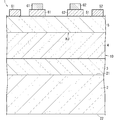
- FIG. 2 is a cross-sectional view of a bidirectional switch element in a switch system including the above control system.
- FIG. 3 is an operation explanatory diagram when the bidirectional switch element is turned on in the control system of the above.
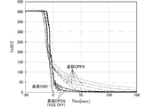
- FIG. 4 is a comparison diagram between a turn-on waveform of a bidirectional switch element in a switch system including the control system and a turn-on waveform of a bidirectional switch element in a switch system according to a comparative example.
- FIG. 1A is a circuit block diagram of a switch system including the control system according to the embodiment.
- FIG. 1B is a circuit configuration diagram of a part of the above control system.
- FIG. 2 is a cross-sectional view of a bidirectional switch element in a switch system including the above control system.
- FIG. 3 is an
- FIG. 5 is an explanatory diagram of the switching speed of the bidirectional switch element in the switch system including the control system according to the embodiment and the switching speed in the comparative example.
- FIG. 6 is an operation explanatory diagram when the bidirectional switch element is turned off in the control system of the above.
- FIG. 7 is a circuit block diagram of a switch system including the control system according to the first modification of the embodiment.
- FIG. 8 is a circuit diagram of a power conversion device including a control system according to a second modification of the embodiment.
- FIG. 9 is a circuit diagram of a power conversion device including a control system according to a third modification of the embodiment.
- FIG. 2 described in the following embodiments and the like is a schematic diagram, and the ratio of the size and thickness of each component in FIG. 2 does not necessarily reflect the actual dimensional ratio. .
- the switch system 200 includes the bidirectional switch element 1 and the above-described control system 100 that controls the bidirectional switch element 1.
- the bidirectional switch element 1 will be described based on FIG. 2, and then the control system 100 will be described.
- Bidirectional switch element 1 (1.1) Configuration of bidirectional switch element
- the bidirectional switch element 1 includes a substrate 2, a first nitride semiconductor layer 4, a second nitride semiconductor layer 5, 1st source electrode S1, 1st gate electrode G1, 2nd gate electrode G2, 2nd source electrode S2, 1st p-type nitride semiconductor layer 61, 2nd p-type nitride A semiconductor layer 62.
- the first nitride semiconductor layer 4 is formed on the substrate 2.
- the second nitride semiconductor layer 5 is formed on the first nitride semiconductor layer 4.
- the second nitride semiconductor layer 5 has a larger band gap than the first nitride semiconductor layer 4.
- the first source electrode S1 is formed on the second nitride semiconductor layer 5.
- the first gate electrode G1 is formed on the second nitride semiconductor layer 5, and is separated from the first source electrode S1.
- the second gate electrode G2 is formed on the second nitride semiconductor layer 5, and on the opposite side of the first source electrode S1 from the first gate electrode G1 when viewed from the first gate electrode G1. is seperated.
- the second source electrode S2 is formed on the second nitride semiconductor layer 5, and is opposite to the first gate electrode G1 when viewed from the second gate electrode G2. is seperated.
- the first p-type nitride semiconductor layer 61 is interposed between the first gate electrode G1 and the second nitride semiconductor layer 5.
- the second p-type nitride semiconductor layer 62 is interposed between the second gate electrode G2 and the second nitride semiconductor layer 5.
- the first nitride semiconductor layer 4, the second nitride semiconductor layer 5, the first p-type nitride semiconductor layer 61, and the second p-type nitride semiconductor layer are formed on the substrate 2. 62 are formed.
- bidirectional switch element 1 will be described in more detail.
- the bidirectional switch element 1 is a dual-gate GaN-based GIT (Gate Injection Transistor).
- the first nitride semiconductor layer 4 is a GaN layer
- the second nitride semiconductor layer 5 is an AlGaN layer.
- the second nitride semiconductor layer 5 is formed on the first nitride semiconductor layer 4, and forms a heterojunction HJ together with the first nitride semiconductor layer 4.
- a two-dimensional electron gas (Two-Dimensional Electron Gas) is generated near the heterojunction HJ.
- a region containing a two-dimensional electron gas (hereinafter, also referred to as a “two-dimensional electron gas layer”) can function as an n-channel layer (electron conductive layer).
- a two-dimensional electron gas layer can function as an n-channel layer (electron conductive layer).
- each of the first p-type nitride semiconductor layer 61 and the second p-type nitride semiconductor layer 62 is a p-type AlGaN layer.
- the substrate 2 is a conductive silicon substrate. Therefore, the substrate 2 is a kind of a conductive substrate.
- the substrate 2 has a first main surface 21 and a second main surface 22.
- the first main surface 21 and the second main surface 22 of the substrate 2 are orthogonal to the thickness direction of the substrate 2.
- the term “orthogonal” is not limited to the case of strictly orthogonal, but is substantially orthogonal (the angle between the thickness direction and the first main surface 21 or the second main surface 22 is, for example, 90 ° ⁇ 5 °). May be.
- the second main surface 22 is located on the opposite side of the first main surface 21 in the thickness direction of the substrate 2.
- the multilayer body 10 is formed on the first main surface 21 of the substrate 2.
- the first main surface 21 of the substrate 2 is, for example, a (111) plane.
- the first main surface 21 of the substrate 2 may be, for example, a crystal plane having an off angle (hereinafter, referred to as “first off angle”) from the (111) plane that is greater than 0 ° and 5 ° or less.
- first off angle is the inclination angle of the first main surface 21 with respect to the (111) plane. Therefore, if the off angle is 0 °, the first main surface 21 is a (111) plane.
- the (111) plane is a crystal plane represented by a Miller index (Miller Index) in which three indices are put in parentheses.
- the thickness of the substrate 2 is, for example, not less than 100 ⁇ m and not more than 1000 ⁇ m.
- the first nitride semiconductor layer 4 is formed on the substrate 2 via the buffer layer 3.
- the above-described laminate 10 includes the buffer layer 3.
- the buffer layer 3, the first nitride semiconductor layer 4, and the second nitride semiconductor layer 5 are arranged in this order from the substrate 2 side.
- the stacked body 10 includes a first p-type nitride semiconductor layer 61 and a second p-type nitride semiconductor layer 62 formed on the second nitride semiconductor layer 5.
- the multilayer body 10 is an epitaxial growth layer grown on the substrate 2 by, for example, MOVPE (Metal Organic Vapor Phase Epitaxy).
- MOVPE Metal Organic Vapor Phase Epitaxy
- TMAl trimethyl aluminum
- TMGa trimethylgallium
- NH 3 NH 3
- Cp 2 Mg Biscyclopentadienyl magnesium
- H 2 gas is preferably used as the carrier gas for each source gas.
- Each source gas is not particularly limited.
- triethyl gallium (TEGa) may be used as a source gas for Ga
- a hydrazine derivative may be used as a source gas for N.
- the buffer layer 3 is, for example, an undoped GaN layer.
- the buffer layer 3 improves the crystallinity of the first nitride semiconductor layer 4, the second nitride semiconductor layer 5, the first p-type nitride semiconductor layer 61, and the second p-type nitride semiconductor layer 62. It is a layer provided for the purpose.
- Buffer layer 3 is formed directly on first main surface 21 of substrate 2.
- the undoped GaN layer constituting the buffer layer 3 may contain impurities such as Mg, H, Si, C, and O which are inevitably mixed during the growth.
- the thickness of the buffer layer 3 is, for example, 100 nm or more and 3000 nm or less.
- the first nitride semiconductor layer 4 is an undoped GaN layer.
- the undoped GaN layer that forms the first nitride semiconductor layer 4 may contain impurities such as Mg, H, Si, C, and O that are inevitably mixed during the growth.
- the thickness of the first nitride semiconductor layer 4 is, for example, not less than 100 nm and not more than 700 nm.
- the second nitride semiconductor layer 5 is an undoped AlGaN layer.
- the undoped AlGaN layer constituting the second nitride semiconductor layer 5 may contain impurities such as Mg, H, Si, C, and O which are inevitably mixed during the growth.
- the Al composition ratio of the undoped AlGaN layer forming the second nitride semiconductor layer 5 is, for example, 0.2. In this specification, the Al composition ratio is a value of x when the AlGaN layer is represented by an Al x Ga 1 -xN layer. That is, the second nitride semiconductor layer 5 is an undoped Al 0.2 Ga 0.8 N layer.
- the composition ratio is, for example, a value obtained by a composition analysis using EDX (Energy Dispersive X-ray Spectroscopy).
- EDX Electronic Dispersive X-ray Spectroscopy
- the composition ratios are not limited to EDX, but are determined by, for example, composition analysis using Auger Electron Spectroscopy, or SIMS (Secondary Ion Mass Spectroscopy). It may be a value.
- the thickness of the second nitride semiconductor layer 5 is, for example, not less than 20 nm and not more than 100 nm.
- Each of the first p-type nitride semiconductor layer 61 and the second p-type nitride semiconductor layer 62 is a p-type AlGaN layer.
- the first p-type nitride semiconductor layer 61 and the second p-type nitride semiconductor layer 62 cover only a part of the surface 51 of the second nitride semiconductor layer 5. Therefore, the surface 51 of the second nitride semiconductor layer 5 has a region covered with the first p-type nitride semiconductor layer 61 and the second p-type nitride semiconductor layer 62 and a first p-type nitride semiconductor layer 62. And a region that is not covered with the semiconductor layer 61 and the second p-type nitride semiconductor layer 62.
- the first p-type nitride semiconductor layer 61 and the second p-type nitride semiconductor layer 62 are apart from each other.
- the first p-type nitride semiconductor layer 61 and the second p-type nitride semiconductor layer 62 are doped with Mg during their growth and contain Mg.
- the first p-type nitride semiconductor layer 61 and the second p-type nitride semiconductor layer 62 are formed from the first p-type nitride semiconductor layer 61 and the second p-type nitride semiconductor layer 62 by MOVPE. Is formed by growing a p-type nitride semiconductor layer on the second nitride semiconductor layer 5 and then patterning the p-type nitride semiconductor layer using a photolithography technique and an etching technique.
- the Al composition ratio of each of the first p-type nitride semiconductor layer 61 and the second p-type nitride semiconductor layer 62 is the same as the Al composition ratio of the AlGaN layer forming the second nitride semiconductor layer 5 (For example, 0.2), but may be different from the Al composition ratio of the AlGaN layer constituting the second nitride semiconductor layer 5.
- the thickness of each of the first p-type nitride semiconductor layer 61 and the second p-type nitride semiconductor layer 62 is, for example, not less than 50 nm and not more than 300 nm.
- the first source electrode S1 and the second source electrode S2 cover the first p-type nitride semiconductor layer 61 and the second p-type nitride semiconductor layer 62 on the surface 51 of the second nitride semiconductor layer 5. It is formed in a region that is not covered.
- the first source electrode S1 and the second source electrode S2 are separated from each other.
- the first source electrode S1 and the second source electrode S2 are electrically connected to the hetero junction HJ.
- “electrically connected” means that they are in ohmic contact.
- Each of the first source electrode S1 and the second source electrode S2 contains, for example, Ti and Al.
- the first gate electrode G1 is formed on the second nitride semiconductor layer 5 with the first p-type nitride semiconductor layer 61 interposed therebetween. Further, the second gate electrode G2 is formed on the second nitride semiconductor layer 5 via the second p-type nitride semiconductor layer 62. The distance between the first gate electrode G1 and the second gate electrode G2 is longer than the distance between the first p-type nitride semiconductor layer 61 and the second p-type nitride semiconductor layer 62. Each of first gate electrode G1 and second gate electrode G2 corresponds to a corresponding first source electrode S1 and second source electrode S2 in a direction along surface 51 of second nitride semiconductor layer 5, respectively.
- the first gate electrode G1 and the second gate electrode G2 are in ohmic contact with, for example, a first p-type nitride semiconductor layer 61 and a second p-type nitride semiconductor layer 62, respectively.
- Each of the first gate electrode G1 and the second gate electrode G2 includes, for example, Pd and Au.
- the first source electrode S1, the first gate electrode G1, the second gate electrode G2, and the second source The electrodes S2 are arranged in this order.
- the first source electrode S1, the first gate electrode G1, the second gate electrode G2, and the second source electrode S2 are separated from each other in the one direction.
- the first gate electrode G1 is also referred to as an off state. Further, a state in which a voltage equal to or higher than a first threshold voltage is applied between the first gate electrode G1 and the first source electrode S1 with the first gate electrode G1 being on the high potential side is referred to as a first gate.
- the electrode G1 is also called an ON state.
- a state in which a voltage equal to or higher than the second threshold voltage is not applied between the second gate electrode G2 and the second source electrode S2 is also referred to as a state in which the second gate electrode G2 is off. Further, a state in which a voltage equal to or higher than a second threshold voltage is applied between the second gate electrode G2 and the second source electrode S2 with the second gate electrode G2 being on the high potential side is referred to as a second gate.
- the electrode G2 is also called an ON state.
- the bidirectional switch element 1 includes the first p-type nitride semiconductor layer 61 and the second p-type nitride semiconductor layer 62 to realize a normally-off transistor.
- the first p-type nitride semiconductor layer 61 is formed between the second p-type nitride semiconductor layer 5 and the second p-type nitride semiconductor layer 5 immediately below the first p-type nitride semiconductor layer 61.
- a depletion layer is formed with the first nitride semiconductor layer 4.
- the second p-type nitride semiconductor layer 62 is formed between the second p-type nitride semiconductor layer 5 and the first nitride semiconductor layer 5 immediately below the second p-type nitride semiconductor layer 62.
- a depletion layer is formed with the semiconductor layer 4.
- the first gate electrode G1 and the first source electrode S1 can be connected by a two-dimensional electron gas layer.
- the two-dimensional electron gas layer is blocked by the depletion layer between the first gate electrode G1 and the first source electrode S1.
- the bidirectional switch element 1 when the second gate electrode G2 is in the ON state, the second gate electrode G2 and the second source electrode S2 can be connected by a two-dimensional electron gas layer. In other words, in the bidirectional switch element 1, when the second gate electrode G2 is on, the two-dimensional electron gas layer is blocked by the depletion layer between the second gate electrode G2 and the second source electrode S2. Gone.
- the first source electrode S1 and the second No current can flow in any direction between the source electrode S2 and the source electrode S2. More specifically, in the case of the first operation mode, a current flowing from the first source electrode S1 to the second source electrode S2 when the first source electrode S1 has a higher potential than the second source electrode S2. When the current is cut off and the second source electrode S2 has a higher potential than the first source electrode S1, the current flowing from the second source electrode S2 to the first source electrode S1 is cut off.
- the first source electrode S1 and the second A current can flow bidirectionally between the source electrode S2 and the source electrode S2. More specifically, in the case of the second operation mode, a current flows from the first source electrode S1 to the second source electrode S2 when the first source electrode S1 has a higher potential than the second source electrode S2. When the second source electrode S2 has a higher potential than the first source electrode S1, a current flows from the second source electrode S2 to the first source electrode S1.
- the bidirectional switch element 1 functions as a diode when the first gate electrode G1 is on and the second gate electrode G2 is off (in the third operation mode). More specifically, in the third operation mode, when the first source electrode S1 has a higher potential than the second source electrode S2, the current flowing from the first source electrode S1 to the second source electrode S2 is cut off. When the second source electrode S2 is at a higher potential than the first source electrode S1 by a second threshold voltage or higher, a current flows from the second source electrode S2 to the first source electrode S1.
- the bidirectional switch element 1 functions as a diode when the first gate electrode G1 is off and the second gate electrode G2 is on (fourth operation mode). More specifically, in the fourth operation mode, when the second source electrode S2 has a higher potential than the first source electrode S1, the current flowing from the second source electrode S2 to the first source electrode S1 is cut off. When the first source electrode S1 is higher than the second source electrode S2 by a first threshold voltage or higher and has a higher potential, a current flows from the first source electrode S1 to the second source electrode S2.
- the first threshold voltage and the second threshold voltage have the same value, but may have different values.
- the first threshold voltage is a threshold value below which the depletion layer extending so as to block the two-dimensional electron gas layer below the first gate electrode G1 is reduced so that current can flow through the two-dimensional electron gas layer.
- the second threshold voltage is a threshold value below which the depletion layer extending so as to block the two-dimensional electron gas layer under the second gate electrode G2 is reduced so that current can flow through the two-dimensional electron gas layer. Voltage.
- the control system 100 includes a control unit 101 as shown in FIG. 1A.
- the control system 100 includes a first gate drive circuit 102 and a second gate drive circuit 103 in addition to the control unit 101.
- a series circuit of an AC power supply 211 and a load 212 is connected between a first source electrode S1 and a second source electrode S2 of the bidirectional switch element 1. Used in the state that is being done.
- the control unit 101, the first gate drive circuit 102, and the second gate drive circuit 103 are supplied with a DC voltage from the power supply circuit 110.
- the power supply circuit 110 includes, for example, a diode bridge that full-wave rectifies the output voltage of an AC power supply (for example, a commercial power supply) 211, a smoothing capacitor that smoothes the output voltage of the diode bridge, and an output voltage of the smoothing capacitor that is a DC voltage. And a step-down chopper circuit.
- the power supply circuit 110 is not a component of the control system 100.
- the circuit configuration of the power supply circuit 110 is not particularly limited.
- the first gate drive circuit 102 applies a first gate voltage Vg1 (see FIG. 3) based on the first source electrode S1 between the first gate electrode G1 and the first source electrode S1. Circuit.
- the first gate drive circuit 102 is controlled by a control signal from the control unit 101 to set the first gate voltage Vg1 to a voltage V1 (for example, 5 V) higher than the first threshold voltage or a voltage higher than the first threshold voltage.
- V1 for example, 5 V
- a small voltage for example, 0 V
- the second gate drive circuit 103 applies a second gate voltage Vg2 (see FIG. 3) based on the second source electrode S2 between the second gate electrode G2 and the second source electrode S2. Circuit.
- the second gate drive circuit 103 is controlled by a control signal from the control unit 101 to set the second gate voltage Vg2 to a voltage V2 (for example, 5 V) higher than the second threshold voltage or higher than the second threshold voltage.
- V2 for example, 5 V
- a small voltage for example, 0 V
- the control unit 101 determines whether the first gate electrode G1 or the second gate electrode G2 is the lower potential side of the first source electrode S1 and the second source electrode S2.
- a time difference ⁇ t between a first timing of applying a voltage equal to or higher than the threshold voltage to the gate electrode corresponding to the source electrode and a second timing of applying a voltage equal to or higher than the threshold voltage to the gate electrode corresponding to the source electrode on the high potential side. (See FIG. 3) to control the bidirectional switch element 1.
- the time difference ⁇ t is preferably, for example, 50 nsec or more in consideration of the margin of the control system 100. Thereby, ⁇ t can be set to 10 nsec or more even if there is fluctuation, variation, or the like of the control system 100.
- the control unit 101 causes the bidirectional switch element 1 to operate as a diode during a period between the first timing and the second timing.
- the bidirectional switch element 1 operates as a diode during this period, the first source electrode S1 and the second source electrode S2 move from a relatively low potential source electrode to a relatively high potential source electrode. No current flows, and current flows from a relatively high potential source electrode to a relatively low potential source electrode.
- the control unit 101 When turning on the bidirectional switch element 1 in a state where the second source electrode S2 is at a higher potential than the first source electrode S1, the control unit 101, as shown in FIG.
- the first gate voltage Vg1 between the second gate electrode G2 and the second source electrode S2 after setting the first gate voltage Vg1 between the second gate electrode G2 and the second source electrode S2 to a value equal to or higher than the first threshold voltage.
- the voltage Vg2 is set to a value equal to or higher than the second threshold voltage.
- the control unit 101 applies the first gate voltage Vg1 between the first gate electrode G1 and the first source electrode S1 (corresponding to the first timing) and the second gate voltage Vg2.
- the bidirectional switch element 1 is set in the third operation mode. Operate as a diode. Thereby, the bidirectional switch element 1 cuts off the current flowing from the first source electrode S1 to the second source electrode S2 when the first source electrode S1 has a higher potential than the second source electrode S2, and When the second source electrode S2 is at a higher potential than the first source electrode S1 by a second threshold voltage or more, a current flows from the second source electrode S2 to the first source electrode S1.
- the execution subject of the control unit 101 includes a computer system.
- the computer system has one or more computers.
- the computer system mainly has a processor and a memory as hardware.
- the processor executes the program recorded in the memory of the computer system, a function as an execution subject of the control unit 101 in the present disclosure is realized.
- the program may be recorded in the memory of the computer system in advance, or may be provided through an electric communication line, or may be provided in a non-temporary storage medium such as a memory card, an optical disk, or a hard disk drive (magnetic disk) readable by the computer system. May be provided by being recorded on a dynamic recording medium.
- a processor of a computer system includes one or more electronic circuits including a semiconductor integrated circuit (IC) or a large-scale integrated circuit (LSI).
- IC semiconductor integrated circuit
- LSI large-scale integrated circuit
- a plurality of electronic circuits may be integrated on one chip, or may be provided separately on a plurality of chips.
- a plurality of chips may be integrated in one device, or may be provided separately in a plurality of devices.
- the control system 100 controls the resistance division circuit 105 as shown in FIG. 1B so that the control unit 101 can determine which of the first source electrode S1 and the second source electrode S2 has the higher potential.
- a detection circuit 104 including a first operational amplifier OP1, a second operational amplifier OP2, a first photocoupler PC1, and a second photocoupler PC2.
- the resistor voltage dividing circuit 105 is a series circuit of a first resistor R1 and a second resistor R2, and is connected between the first source electrode S1 and the second source electrode S2 of the bidirectional switch element 1.
- the non-inverting input terminal of the first operational amplifier OP1 and the inverting input terminal of the second operational amplifier OP2 are connected to a connection point between the first resistor R1 and the second resistor R2 of the resistor voltage dividing circuit 105.
- the voltage between the first source electrode S1 and the second source electrode S2 is applied to the non-inverting input terminal of the first operational amplifier OP1 and the inverting input terminal of the second operational amplifier OP2.
- the inverting input terminal of the first operational amplifier OP1 and the non-inverting input terminal of the second operational amplifier OP2 are connected to the first source electrode S1, and are grounded.
- the output terminal of the first operational amplifier OP1 is connected to the anode terminal of the LED (Light Emitting Diode) of the first photocoupler PC1 via the fourth resistor R4, and the output terminal of the second operational amplifier OP2 is connected to the fifth terminal. Is connected to the anode terminal of the LED of the second photocoupler PC2 via the resistor R5.
- the cathode terminal of the LED of the first photocoupler PC1 and the cathode terminal of the LED of the second photocoupler PC2 are connected to the first source electrode S1 and are grounded.
- the phototransistor of the first photocoupler PC1 and the phototransistor of the second photocoupler PC2 are connected to the control unit 101.
- the control unit 101 determines which of the first source electrode S1 and the second source electrode S2 has a higher potential. Can be determined. Note that the configuration of the detection circuit 104 is not limited to the example in FIG. 1B.
- FIG. 4 shows a case where the bidirectional switch element 1 is turned on with a series circuit of a DC power supply and a load connected between the first source electrode S1 and the second source electrode S2 of the bidirectional switch element 1.
- FIG. 4 shows the voltage when the bidirectional switch element 1 is turned on with the positive electrode of the DC power supply connected to the second source electrode S2 and the negative electrode of the DC power supply connected to the first source electrode S1. It is a waveform.
- the vertical axis in FIG. 4 is the voltage Vs2 between the second source electrode S2 and the first source electrode S1, and the horizontal axis is time.
- the right side is “positive” and the left side is “negative ( ⁇ sign)” with reference to time 0 nsec, but “positive” and “negative ( ⁇ sign)” This is a code added to distinguish whether the time is after or before.
- the substrate OPEN (VG2 OFF) in FIG. 4 is Vs2 when the control system 100 according to the first embodiment turns on the bidirectional switch element 1 in a state where the substrate 2 of the bidirectional switch element 1 is electrically floating.
- the “state in which the substrate 2 is electrically floating” means that the substrate 2 is connected to all of the first source electrode S1, the second source electrode S2, the first gate electrode G1, and the second gate electrode G2. On the other hand, it is in a state of being electrically insulated.
- the substrate OPEN (VG2 OFF) in FIG. 4 shows the time change of each Vs2 when the load current is different, and the switching speed increases as the load current decreases.
- the substrate GND in FIG. 4 has the first gate electrode G1 of the bidirectional switch element 1 that is larger than the first threshold voltage when the substrate 2 of the bidirectional switch element 1 is grounded to the ground.
- the timing of applying the gate voltage and the timing of applying the second gate voltage larger than the second threshold voltage to the second gate electrode G2 are the same, and Vs2 when turning on the bidirectional switch element 1 is determined. The time change is shown.
- the substrate 2 of the bidirectional switch element 1 is electrically floating, and the first gate electrode G1 of the bidirectional switch element 1 has a first gate electrode G1 larger than the first threshold voltage. 1 and the timing of applying the second gate voltage larger than the second threshold voltage to the second gate electrode G2 at the same time when the bidirectional switch element 1 is turned on. The time change of Vs2 is shown. Further, the substrate OPEN in FIG. 4 shows the time change of each Vs2 when the load current is different, and the switching speed is faster as the load current is smaller.
- FIG. 5 shows the relationship between the load current and the switching speed of the bidirectional switch element 1.
- the horizontal axis of FIG. 5 is the load current
- the vertical axis is the absolute value of dV / dt corresponding to the switching speed of the bidirectional switch element 1 at turn-on.
- the load current is a current flowing through the load.
- dV / dt is a value obtained by dividing a voltage change when the voltage Vs2 decreases from a value of 90% of the maximum value to a value of 10% by time.
- the timing at which the first gate voltage Vg1 is changed from the voltage V1 to 0V and the timing at which the second gate voltage Vg2 is changed from the voltage V2 to 0V are:
- the relationship is not particularly limited. However, from the viewpoint of reducing the loss in the bidirectional switch element 1, when the control unit 101 of the control system 100 turns off the bidirectional switch element 1, it is preferable not to operate the bidirectional switch element 1 as a diode.
- the control unit 101 changes the timing at which the first gate voltage Vg1 is changed from the voltage V1 to 0V and the time at which the second gate voltage Vg2 is changed to the voltage V2.
- the bidirectional switch element 1 is not operated as a diode by aligning the timing of changing the voltage from 0 V to 0 V.
- the control method of the bidirectional switch element 1 is the first gate electrode G1 or the second gate electrode G2 and the first source electrode S1 and the second source electrode S2.
- a first timing of applying a voltage higher than a threshold voltage to a gate electrode corresponding to a source electrode on a lower potential side, and a second timing of applying a voltage higher than the threshold voltage to a gate electrode corresponding to a source electrode on a higher potential side is controlled so as to cause a time difference ⁇ t.
- the above-mentioned program causes the computer system that controls the bidirectional switch element 1 to turn on the bidirectional switch element 1 when the first gate electrode G1 or the second gate electrode G2 and the first source electrode S1
- This is a program for executing a delay process that causes a time difference ⁇ t between the second timing for applying the voltage and the second timing for applying the voltage.
- FIG. 7 is a circuit block diagram of a switch system 200a including the control system 100a according to the first modification of the embodiment.
- the same components as those of the switch system 200 including the control system 100 (see FIG. 1A) according to the embodiment are denoted by the same reference numerals and description thereof is omitted. I do.
- the control unit 101a when the bidirectional switch element 1 is turned on, the control unit 101a is the first gate electrode G1 or the second gate electrode G2 and the first source electrode A first timing of applying a voltage equal to or higher than a threshold voltage to a gate electrode corresponding to a source electrode on a lower potential side of S1 and a second source electrode S2, and a threshold voltage being applied to a gate electrode corresponding to a source electrode on a higher potential side
- the bidirectional switch element 1 is controlled so as to cause a time difference ⁇ t (see FIG. 3) between the above-described second timing of applying the voltage.
- control unit 101a is configured by an analog circuit, and includes a delay circuit 111 that generates a time difference ⁇ t.
- a switch system 200b including the control system 100b according to the second modification of the embodiment and a power conversion device 300b including the switch system 200b will be described with reference to FIG.
- the power converter 300b is a matrix converter that performs AC-AC power conversion.
- the power converter 300b converts the first AC voltage of the first frequency into a second AC voltage of a second frequency different from the first frequency.
- the second frequency is lower than the first frequency.
- the power conversion device 300b includes two input terminals T1 and T2 for inputting the first AC voltage. Further, the power conversion device 300b includes three output terminals T3, T4, and T5 for outputting the second AC voltage.
- the first AC voltage is a single-phase AC voltage
- the second AC voltage is a three-phase AC voltage.
- the power conversion device 300b includes six switching elements Q1 to Q6 each including the bidirectional switch element 1. Note that, for example, a three-phase AC motor is connected as a load to the three output terminals T3, T4, and T5.
- a series circuit of the switching elements Q1 and Q2, a series circuit of the switching elements Q3 and Q4, and a series circuit of the switching elements Q5 and Q6 are connected in parallel. Each series circuit is connected between two input terminals T1 and T2.
- One output terminal T3 of the three output terminals T3, T4, T5 is connected to a connection point of the switching elements Q1, Q2, and another output terminal T4 is connected to a connection point of the switching elements Q3, Q4. Is connected to a connection point of the switching elements Q5 and Q6.
- the power conversion unit that performs power conversion includes six switching elements Q1 to Q6.
- the power conversion device 300b includes a power conversion unit that includes the bidirectional switch element 1 and performs power conversion, and a control system 100b.
- the control unit 101b in the control system 100b included in the power conversion device 300b controls the plurality of bidirectional switch elements 1 (switching elements Q1 to Q6).
- the control unit 101b is the first gate electrode G1 or the second gate electrode G2, and the first source electrode S1 and the second source electrode
- the bidirectional switch element 1 is controlled so as to cause a time difference ⁇ t (FIG. 3) between the two timings.
- a switch system 200c including the control system 100c according to Modification 3 of the embodiment and a power conversion device 300c including the switch system 200c will be described with reference to FIG.
- the power converter 300c is a T-type three-level inverter.
- the power conversion device 300c includes a series circuit of two switching elements Q11 and Q12, a diode D1 connected in antiparallel to the switching element Q11, a diode D2 connected in antiparallel to the switching element Q12, A bidirectional switch element 1 connected to a connection point between the two switching elements Q11 and Q12.
- Each of the two switching elements Q11 and Q12 is an IGBT (Insulated Gate Bipolar Transistor).
- the power conversion unit that performs power conversion includes a series circuit of the two switching elements Q11 and Q12, a diode D1 connected in antiparallel to the switching element Q11, and an antiparallel to the switching element Q12. It includes a connected diode D2 and a bidirectional switch element 1 connected to a connection point between two switching elements Q11 and Q12.
- the power conversion device 300c includes a power conversion unit that includes the bidirectional switch element 1 and performs power conversion, and a control system 100c.
- the control unit 101c in the control system 100c included in the power conversion device 300c controls the bidirectional switch element 1.
- the control unit 101c determines whether the first gate electrode G1 or the second gate electrode G2 is the first source electrode S1 and the second source electrode S2.
- the bidirectional switch element 1 is controlled so as to cause a time difference ⁇ t (FIG. 3).
- the control unit 101c controls not only the bidirectional switch element 1 but also the two switching elements Q11 and Q12, but may be configured to control only the bidirectional switch element 1.
- the above embodiment is just one of various embodiments of the present disclosure.
- the above embodiment can be variously modified according to the design and the like as long as the object of the present disclosure can be achieved.
- each of the first p-type nitride semiconductor layer 61 and the second p-type nitride semiconductor layer 62 is not limited to the p-type AlGaN layer, but may be, for example, a p-type GaN layer.
- the bidirectional switch element 1 may include one or more nitride semiconductor layers between the buffer layer 3 and the first nitride semiconductor layer 4. Further, the buffer layer 3 is not limited to a single-layer structure, and may have, for example, a superlattice structure.
- the substrate 2 is not limited to a silicon substrate, but may be, for example, a GaN substrate, a SiC substrate, a sapphire substrate, or the like.
- the control system 100 may include a first power supply and a second power supply controlled by the control unit 101 instead of the first gate drive circuit 102 and the second gate drive circuit 103.
- the first power supply outputs the first gate voltage Vg1 under the control of the control unit 101
- the second power supply outputs the second gate voltage Vg2 under the control of the control unit 101.
- the power converter may have a configuration other than the power converters 300b and 300c described above.
- the control system (100; 100a; 100b; 100c) is a system that controls the bidirectional switch element (1).
- the bidirectional switch element (1) includes a substrate (2), a first nitride semiconductor layer (4), a second nitride semiconductor layer (5), a first source electrode (S1), A first gate electrode (G1), a second gate electrode (G2), a second source electrode (S2), a first p-type nitride semiconductor layer (61), and a second p-type nitride.
- the first nitride semiconductor layer (4) is formed on the substrate (2).
- the second nitride semiconductor layer (5) is formed on the first nitride semiconductor layer (4).
- the band gap of the second nitride semiconductor layer (5) is larger than the band gap of the first nitride semiconductor layer (4).
- the first source electrode (S1), the first gate electrode (G1), the second gate electrode (G2), and the second source electrode (S2) are formed on the second nitride semiconductor layer (5). Is formed.
- the first p-type nitride semiconductor layer (61) is interposed between the first gate electrode (G1) and the second nitride semiconductor layer (5).
- the second p-type nitride semiconductor layer (62) is interposed between the second gate electrode (G2) and the second nitride semiconductor layer (5).
- the control system (100; 100a; 100b; 100c) includes a control unit (101; 101a; 101b; 101c).
- the control unit (101; 101a; 101b; 101c) is the first gate electrode (G1) or the second gate electrode (G2) and is the first source electrode.
- the bidirectional switch element (1) is controlled so as to cause a time difference ( ⁇ t) between the second timing of applying a voltage equal to or higher than the threshold voltage to the electrode.
- the control system (100; 100a; 100b; 100c) according to the first aspect can improve the switching speed when turning on the bidirectional switch element (1).
- the control unit (101; 101a; 101b; 101c) sets a period between the first timing and the second timing.
- the bidirectional switch element (1) is operated as a diode.
- the bidirectional switch element (1) has a relatively high potential from a relatively low potential of the first source electrode (S1) and the second source electrode (S2). No current flows to the source electrode, and current flows from a source electrode having a relatively high potential to a source electrode having a relatively low potential.
- the switching speed when turning on the bidirectional switch element (1) can be more reliably improved.
- the time difference ( ⁇ t) is 50 nsec or more.
- a time difference ( ⁇ t) can be ensured even if system fluctuations or variations occur.
- the substrate (2) includes a first source electrode (S1) and a second source electrode (S1).
- the source electrode (S2), the first gate electrode (G1), and the second gate electrode (G2) are all electrically insulated.
- the substrate (2) includes the first source electrode (S1), the second source electrode (S2), and the first gate electrode (G1).
- the substrate (2) includes the first source electrode (S1), the second source electrode (S2), and the first gate electrode (G1).
- the second gate electrodes (G2) are electrically insulated, it is possible to more reliably improve the switching speed when turning on the bidirectional switch element (1).
- control section (101a) includes a delay circuit (111) for generating a time difference ( ⁇ t).
- control unit (101; 101a; 101b; 101c) includes a bidirectional switch element ( When turning off 1), the bidirectional switch element (1) is not operated as a diode.
- the control system (100; 100a; 100b; 100c) according to the sixth aspect can suppress loss in the bidirectional switch element (1) when the bidirectional switch element (1) is turned off.
- a switch system (200; 200a; 200b; 200c) according to a seventh aspect includes a control system (100; 100a; 100b; 100c) according to any one of the first to sixth aspects, and a bidirectional switch element (1).
- the switch system (200; 200a; 200b; 200c) according to the seventh aspect can improve the switching speed when turning on the bidirectional switch element (1).
- the power converter (300b; 300c) according to the eighth aspect includes the switch system (200b; 200c) according to the seventh aspect.
- the power conversion device (300b; 300c) according to the eighth aspect can improve the switching speed when turning on the bidirectional switch element (1).
- the bidirectional switch element (1) includes a substrate (2), a first nitride semiconductor layer (4), and a second nitride.
- the semiconductor device includes a p-type nitride semiconductor layer (61) and a second p-type nitride semiconductor layer (62).
- the first nitride semiconductor layer (4) is formed on the substrate (2).
- the second nitride semiconductor layer (5) is formed on the first nitride semiconductor layer (4).
- the band gap of the second nitride semiconductor layer (5) is larger than the band gap of the first nitride semiconductor layer (4).
- the first source electrode (S1), the first gate electrode (G1), the second gate electrode (G2), and the second source electrode (S2) are formed on the second nitride semiconductor layer (5). Is formed.
- the first p-type nitride semiconductor layer (61) is interposed between the first gate electrode (G1) and the second nitride semiconductor layer (5).
- the second p-type nitride semiconductor layer (62) is interposed between the second gate electrode (G2) and the second nitride semiconductor layer (5).
- the control method of the bidirectional switch element (1) is the first gate electrode (G1) or the second gate electrode (G2) and the first source electrode (G2).
- the bidirectional switch element (1) is controlled so as to cause a time difference ( ⁇ t) between the second timing at which a voltage equal to or higher than the threshold voltage is applied.
- the control method of the bidirectional switch element according to the ninth aspect makes it possible to improve the switching speed when turning on the bidirectional switch element (1).
- the program according to the tenth aspect includes a substrate (2), a first nitride semiconductor layer (4), a second nitride semiconductor layer (5), a first source electrode (S1), A first gate electrode (G1), a second gate electrode (G2), a second source electrode (S2), a first p-type nitride semiconductor layer (61), and a second p-type nitride.
- the threshold voltage of the gate electrode corresponding to the source electrode on the high potential side is higher than the threshold voltage
- a second timing of applying the voltage, to two hours difference delay processing to cause (Delta] t) is executed, a program for.
- the first nitride semiconductor layer (4) is formed on the substrate (2).
- the second nitride semiconductor layer (5) is formed on the first nitride semiconductor layer (4).
- the band gap of the second nitride semiconductor layer (5) is larger than the band gap of the first nitride semiconductor layer (4).
- the first source electrode (S1), the first gate electrode (G1), the second gate electrode (G2), and the second source electrode (S2) are formed on the second nitride semiconductor layer (5). Is formed.
- the first p-type nitride semiconductor layer (61) is interposed between the first gate electrode (G1) and the second nitride semiconductor layer (5).
- the second p-type nitride semiconductor layer (62) is interposed between the second gate electrode (G2) and the second nitride semiconductor layer (5).
- the program according to the tenth aspect makes it possible to improve the switching speed when turning on the bidirectional switch element (1).
Landscapes
- Engineering & Computer Science (AREA)
- Power Engineering (AREA)
- Junction Field-Effect Transistors (AREA)
- Electronic Switches (AREA)
Abstract
本開示の課題は、双方向スイッチ素子をターンオンさせるときのスイッチング速度を向上させることである。制御システム(100)は、制御部(101)を備える。制御部(101)は、双方向スイッチ素子(1)をターンオンさせる場合、第1のゲート電極(G1)又は第2のゲート電極(G2)であって第1のソース電極(S1)と第2のソース電極(S2)とのうち低電位側のソース電極に対応するゲート電極に閾値電圧以上の電圧を印加する第1タイミングと、高電位側のソース電極に対応するゲート電極に閾値電圧以上の電圧を印加する第2タイミングと、に時間差を生じさせるように双方向スイッチ素子(1)を制御する。
Description
本開示は、制御システム、スイッチシステム、電力変換装置、双方向スイッチ素子の制御方法及びプログラムに関し、より詳細には、2つのゲート電極を備える双方向スイッチ素子を制御する制御システム、その制御システムを備えるスイッチシステム、そのスイッチシステムを備える電力変換装置、双方向スイッチ素子の制御方法、及びプログラムに関する。
従来、ダブルゲート(デュアルゲート)の半導体素子である双方向スイッチ素子が提案されている(特許文献1)。
特許文献1に記載された双方向スイッチ素子は、シリコンからなる導電性の基板上にAlNからなるバッファ層を介在させて、半導体層積層体が形成されている。半導体層積層体は、アンドープのGaNからなる第1の層(GaN層)と、アンドープのAlGaNからなる第2の層(第1のAlGaN層)とが下側から順次積層されている。
第1の層の第2の層とのヘテロ界面近傍には、2次元電子ガス層であるチャネル領域が生成されている。
半導体層積層体の上には、互いに間隔をおいて第1のオーミック電極(第1のソース電極)及び第2のオーミック電極(第2のソース電極)が形成されている。半導体層積層体の上における第1のオーミック電極と第2のオーミック電極との間の領域に、第1のオーミック電極側から順に、第1のp型窒化物半導体層を介在させて形成された第1のゲート電極と、第2のp型窒化物半導体層を介在させて形成された第2のゲート電極と、が並んでいる。
特許文献1に記載の双方向スイッチ素子では、例えば基板を電気的にフローティングにした状態で使用された場合に、基板を接地して使用した場合と比べて、ターンオン時のスイッチング速度が遅くなってしまうという課題があった。
本開示の目的は、双方向スイッチ素子をターンオンさせるときのスイッチング速度を向上させることが可能な制御システム、スイッチシステム、電力変換装置、双方向スイッチ素子の制御方法及びプログラムを提供することにある。
本開示に係る一態様の制御システムは、双方向スイッチ素子を制御するシステムである。前記双方向スイッチ素子は、基板と、第1の窒化物半導体層と、第2の窒化物半導体層と、第1のソース電極と、第1のゲート電極と、第2のゲート電極と、第2のソース電極と、第1のp型窒化物半導体層と、第2のp型窒化物半導体層と、を備える。前記第1の窒化物半導体層は、前記基板上に形成されている。前記第2の窒化物半導体層は、前記第1の窒化物半導体層上に形成されている。前記第2の窒化物半導体層のバンドギャップは、前記第1の窒化物半導体層のバンドギャップよりも大きい。前記第1のソース電極、前記第1のゲート電極、前記第2のゲート電極、及び前記第2のソース電極は、前記第2の窒化物半導体層上に形成されている。前記第1のp型窒化物半導体層は、前記第1のゲート電極と前記第2の窒化物半導体層との間に介在している。前記第2のp型窒化物半導体層は、前記第2のゲート電極と前記第2の窒化物半導体層との間に介在している。前記制御システムは、制御部を備える。前記制御部は、前記双方向スイッチ素子をターンオンさせる場合、前記第1のゲート電極又は前記第2のゲート電極であって前記第1のソース電極と前記第2のソース電極とのうち低電位側のソース電極に対応するゲート電極に閾値電圧以上の電圧を印加する第1タイミングと、高電位側のソース電極に対応するゲート電極に閾値電圧以上の電圧を印加する第2タイミングと、に時間差を生じさせるように前記双方向スイッチ素子を制御する。
本開示に係る一態様のスイッチシステムは、前記制御システムと、前記双方向スイッチ素子と、を備える。
本開示に係る一態様の電力変換装置は、前記スイッチシステムを備える。
本開示に係る一態様の双方向スイッチ素子の制御方法では、前記双方向スイッチ素子は、基板と、第1の窒化物半導体層と、第2の窒化物半導体層と、第1のソース電極と、第1のゲート電極と、第2のゲート電極と、第2のソース電極と、第1のp型窒化物半導体層と、第2のp型窒化物半導体層と、を備える。前記第1の窒化物半導体層は、前記基板上に形成されている。前記第2の窒化物半導体層は、前記第1の窒化物半導体層上に形成されている。前記第2の窒化物半導体層のバンドギャップは、前記第1の窒化物半導体層のバンドギャップよりも大きい。前記第1のソース電極、前記第1のゲート電極、前記第2のゲート電極、及び前記第2のソース電極は、前記第2の窒化物半導体層上に形成されている。前記第1のp型窒化物半導体層は、前記第1のゲート電極と前記第2の窒化物半導体層との間に介在している。前記第2のp型窒化物半導体層は、前記第2のゲート電極と前記第2の窒化物半導体層との間に介在している。前記双方向スイッチ素子の制御方法は、前記双方向スイッチ素子をターンオンさせる場合、前記第1のゲート電極又は前記第2のゲート電極であって前記第1のソース電極と前記第2のソース電極とのうち低電位側のソース電極に対応するゲート電極に閾値電圧以上の電圧を印加する第1タイミングと、高電位側のソース電極に対応するゲート電極に閾値電圧以上の電圧を印加する第2タイミングと、に時間差を生じさせるように前記双方向スイッチ素子を制御する。
本開示に係る一態様のプログラムは、基板と、第1の窒化物半導体層と、第2の窒化物半導体層と、第1のソース電極と、第1のゲート電極と、第2のゲート電極と、第2のソース電極と、第1のp型窒化物半導体層と、第2のp型窒化物半導体層と、を備える双方向スイッチ素子を制御するコンピュータシステムに、前記双方向スイッチ素子をターンオンさせる場合、前記第1のゲート電極又は前記第2のゲート電極であって前記第1のソース電極と前記第2のソース電極とのうち低電位側のソース電極に対応するゲート電極に閾値電圧以上の電圧を印加する第1タイミングと、高電位側のソース電極に対応するゲート電極に閾値電圧以上の電圧を印加する第2タイミングと、に時間差を生じさせる遅延処理を実行させる、ためのプログラムである。前記第1の窒化物半導体層は、前記基板上に形成されている。前記第2の窒化物半導体層は、前記第1の窒化物半導体層上に形成されている。前記第2の窒化物半導体層のバンドギャップは、前記第1の窒化物半導体層のバンドギャップよりも大きい。前記第1のソース電極、前記第1のゲート電極、前記第2のゲート電極、及び前記第2のソース電極は、前記第2の窒化物半導体層上に形成されている。前記第1のp型窒化物半導体層は、前記第1のゲート電極と前記第2の窒化物半導体層との間に介在している。前記第2のp型窒化物半導体層は、前記第2のゲート電極と前記第2の窒化物半導体層との間に介在している。
下記の実施形態等において説明する図2は、模式的な図であり、図2中の各構成要素の大きさや厚さそれぞれの比が、必ずしも実際の寸法比を反映しているとは限らない。
(実施形態)
以下では、実施形態に係る制御システム100を備えるスイッチシステム200について、図1A及び1Bに基づいて説明する。
以下では、実施形態に係る制御システム100を備えるスイッチシステム200について、図1A及び1Bに基づいて説明する。
スイッチシステム200は、双方向スイッチ素子1と、双方向スイッチ素子1を制御する、上述の制御システム100と、を備える。
以下では、まず双方向スイッチ素子1について、図2に基づいて説明してから制御システム100について説明する。
(1)双方向スイッチ素子
(1.1)双方向スイッチ素子の構成
双方向スイッチ素子1は、基板2と、第1の窒化物半導体層4と、第2の窒化物半導体層5と、第1のソース電極S1と、第1のゲート電極G1と、第2のゲート電極G2と、第2のソース電極S2と、第1のp型窒化物半導体層61と、第2のp型窒化物半導体層62と、を備える。
(1.1)双方向スイッチ素子の構成
双方向スイッチ素子1は、基板2と、第1の窒化物半導体層4と、第2の窒化物半導体層5と、第1のソース電極S1と、第1のゲート電極G1と、第2のゲート電極G2と、第2のソース電極S2と、第1のp型窒化物半導体層61と、第2のp型窒化物半導体層62と、を備える。
第1の窒化物半導体層4は、基板2上に形成されている。第2の窒化物半導体層5は、第1の窒化物半導体層4上に形成されている。第2の窒化物半導体層5は、第1の窒化物半導体層4よりもバンドギャップが大きい。第1のソース電極S1は、第2の窒化物半導体層5上に形成されている。第1のゲート電極G1は、第2の窒化物半導体層5上に形成されており、第1のソース電極S1から離れている。第2のゲート電極G2は、第2の窒化物半導体層5上に形成されており、第1のゲート電極G1から見て第1のソース電極S1とは反対側において第1のゲート電極G1から離れている。第2のソース電極S2は、第2の窒化物半導体層5上に形成されており、第2のゲート電極G2から見て第1のゲート電極G1とは反対側において第2のゲート電極G2から離れている。第1のp型窒化物半導体層61は、第1のゲート電極G1と第2の窒化物半導体層5との間に介在している。第2のp型窒化物半導体層62は、第2のゲート電極G2と第2の窒化物半導体層5との間に介在している。双方向スイッチ素子1では、基板2上に、第1の窒化物半導体層4と第2の窒化物半導体層5と第1のp型窒化物半導体層61及び第2のp型窒化物半導体層62とを含む積層体10が形成されている。
以下、双方向スイッチ素子1について、より詳細に説明する。
双方向スイッチ素子1は、デュアルゲート型のGaN系GIT(Gate Injection Transistor)である。ここにおいて、双方向スイッチ素子1では、第1の窒化物半導体層4がGaN層であり、第2の窒化物半導体層5がAlGaN層である。第2の窒化物半導体層5は、第1の窒化物半導体層4上に形成されており、第1の窒化物半導体層4と共にヘテロ接合部HJを構成する。第1の窒化物半導体層4においては、ヘテロ接合部HJの近傍に、2次元電子ガス(Two-Dimensional Electron Gas)が発生している。2次元電子ガスを含む領域(以下、「2次元電子ガス層」ともいう)は、nチャネル層(電子伝導層)として機能することが可能である。また、双方向スイッチ素子1では、第1のp型窒化物半導体層61及び第2のp型窒化物半導体層62の各々がp型AlGaN層である。
基板2は、導電性のシリコン基板である。したがって、基板2は、導電性基板の一種である。基板2は、第1主面21及び第2主面22を有する。基板2の第1主面21及び第2主面22は、基板2の厚さ方向に直交する。ここにおいて、「直交」とは、厳密に直交する場合のみに限定されず、略直交(厚さ方向と第1主面21又は第2主面22とのなす角度が例えば90°±5°)でもよい。第2主面22は、基板2の厚さ方向において第1主面21の反対側に位置している。双方向スイッチ素子1では、積層体10は、基板2の第1主面21上に形成されている。基板2の第1主面21は、例えば、(111)面である。基板2の第1主面21は、例えば、(111)面からのオフ角(以下、「第1オフ角」という)が0°よりも大きく5°以下の結晶面でもよい。ここにおいて、「第1オフ角」とは、(111)面に対する第1主面21の傾斜角である。したがって、オフ角が0°であれば、第1主面21は、(111)面である。(111)面は、3つの指数を括弧のなかに入れて表記したミラー指数(Miller Index)による結晶面である。基板2の厚さは、例えば、100μm以上1000μm以下である。
第1の窒化物半導体層4は、バッファ層3を介して基板2上に形成されている。ここにおいて、上述の積層体10は、バッファ層3を含む。積層体10では、バッファ層3、第1の窒化物半導体層4及び第2の窒化物半導体層5は、基板2側からこの順に並んでいる。また、積層体10は、第2の窒化物半導体層5上に形成されている第1のp型窒化物半導体層61及び第2のp型窒化物半導体層62を含んでいる。
積層体10は、基板2上に例えばMOVPE(Metal Organic Vapor Phase Epitaxy)によって成長されたエピタキシャル成長層である。基板2上に積層体10を成長させるエピタキシャル成長装置としてMOVPE装置を採用する場合、Alの原料ガスとしては、トリメチルアルミニウム(TMAl)を採用するのが好ましい。また、Gaの原料ガスとしては、トリメチルガリウム(TMGa)を採用するのが好ましい。Nの原料ガスとしては、NH3を採用するのが好ましい。p型導電性に寄与する不純物であるMgの原料ガスとしては、ビスシクロペンタジエニルマグネシウム(Cp2Mg)を採用するのが好ましい。各原料ガスそれぞれのキャリアガスとしては、例えば、H2ガスを採用するのが好ましい。各原料ガスは、特に限定されず、例えば、Gaの原料ガスとしてトリエチルガリウム(TEGa)、Nの原料ガスとしてヒドラジン誘導体を採用してもよい。
バッファ層3は、例えば、アンドープのGaN層である。バッファ層3は、第1の窒化物半導体層4、第2の窒化物半導体層5、第1のp型窒化物半導体層61及び第2のp型窒化物半導体層62の結晶性の向上を目的として設けた層である。バッファ層3は、基板2の第1主面21上に直接形成されている。バッファ層3を構成するアンドープのGaN層は、その成長時に不可避的に混入されるMg、H、Si、C、O等の不純物が存在してもよい。バッファ層3の厚さは、例えば、100nm以上3000nm以下である。
第1の窒化物半導体層4は、アンドープのGaN層である。第1の窒化物半導体層4を構成するアンドープのGaN層は、その成長時に不可避的に混入されるMg、H、Si、C、O等の不純物が存在してもよい。第1の窒化物半導体層4の厚さは、例えば、100nm以上700nm以下である。
第2の窒化物半導体層5は、アンドープのAlGaN層である。第2の窒化物半導体層5を構成するアンドープのAlGaN層は、その成長時に不可避的に混入されるMg、H、Si、C、O等の不純物が存在してもよい。第2の窒化物半導体層5を構成するアンドープのAlGaN層のAlの組成比は、例えば、0.2である。本明細書において、Alの組成比とは、AlGaN層をAlxGa1-xN層で表したときのxの値である。つまり、第2の窒化物半導体層5は、アンドープのAl0.2Ga0.8N層である。組成比は、例えば、EDX(Energy Dispersive X-ray Spectroscopy)による組成分析で求めた値である。組成比の相対的な大小関係を議論する上では、組成比は、EDXに限らず、例えば、オージェ電子分光(Auger Electron Spectroscopy)による組成分析、SIMS(Secondary Ion Mass Spectroscopy)による組成分析で求めた値でもよい。第2の窒化物半導体層5の厚さは、例えば、20nm以上100nm以下である。
第1のp型窒化物半導体層61及び第2のp型窒化物半導体層62の各々は、p型AlGaN層である。
第1のp型窒化物半導体層61及び第2のp型窒化物半導体層62は、第2の窒化物半導体層5の表面51の一部のみを覆っている。したがって、第2の窒化物半導体層5の表面51は、第1のp型窒化物半導体層61及び第2のp型窒化物半導体層62に覆われている領域と、第1のp型窒化物半導体層61及び第2のp型窒化物半導体層62に覆われていない領域と、を含む。第1のp型窒化物半導体層61と第2のp型窒化物半導体層62とは、互いに離れている。第1のp型窒化物半導体層61及び第2のp型窒化物半導体層62は、その成長時にMgがドーピングされており、Mgを含有している。第1のp型窒化物半導体層61及び第2のp型窒化物半導体層62は、MOVPE装置によって第1のp型窒化物半導体層61と第2のp型窒化物半導体層62との元になるp型窒化物半導体層を第2の窒化物半導体層5上に成長させた後に、フォトリソグラフィ技術及びエッチング技術を利用してp型窒化物半導体層をパターニングすることによって形成されている。
第1のp型窒化物半導体層61及び第2のp型窒化物半導体層62の各々のAlの組成比は、第2の窒化物半導体層5を構成するAlGaN層のAlの組成比と同じ(例えば、0.2)であるが、第2の窒化物半導体層5を構成するAlGaN層のAlの組成比と異なっていてもよい。第1のp型窒化物半導体層61及び第2のp型窒化物半導体層62の各々の厚さは、例えば、50nm以上300nm以下である。
第1のソース電極S1及び第2のソース電極S2は、第2の窒化物半導体層5の表面51において第1のp型窒化物半導体層61及び第2のp型窒化物半導体層62に覆われていない領域に形成されている。第1のソース電極S1と第2のソース電極S2とは、互いに離れている。第1のソース電極S1及び第2のソース電極S2は、ヘテロ接合部HJと電気的に接続されている。ここにおいて、「電気的に接続されている」とはオーミック接触していることを意味する。第1のソース電極S1及び第2のソース電極S2の各々は、例えば、TiとAlとを含んでいる。
第1のゲート電極G1は、第1のp型窒化物半導体層61を介して第2の窒化物半導体層5上に形成されている。また、第2のゲート電極G2は、第2のp型窒化物半導体層62を介して第2の窒化物半導体層5上に形成されている。第1のゲート電極G1と第2のゲート電極G2との距離は、第1のp型窒化物半導体層61と第2のp型窒化物半導体層62との距離よりも長い。第1のゲート電極G1及び第2のゲート電極G2の各々は、第2の窒化物半導体層5の表面51に沿った方向において、対応する第1のソース電極S1及び第2のソース電極S2それぞれから離れている。第1のゲート電極G1及び第2のゲート電極G2は、例えば、第1のp型窒化物半導体層61及び第2のp型窒化物半導体層62にそれぞれオーミック接触している。第1のゲート電極G1及び第2のゲート電極G2の各々は、例えば、PdとAuとを含んでいる。
双方向スイッチ素子1では、第2の窒化物半導体層5の表面51に沿った一方向において、第1のソース電極S1、第1のゲート電極G1、第2のゲート電極G2及び第2のソース電極S2が、この順に並んでいる。第1のソース電極S1、第1のゲート電極G1、第2のゲート電極G2及び第2のソース電極S2は、上記一方向において互いに離れている。
(1.2)双方向スイッチ素子の動作
以下では、説明の便宜上、第1のゲート電極G1と第1のソース電極S1との間に第1の閾値電圧以上の電圧が印加されていない状態を、第1のゲート電極G1がオフ状態ともいう。また、第1のゲート電極G1と第1のソース電極S1との間に第1のゲート電極G1を高電位側として第1の閾値電圧以上の電圧が印加されている状態を、第1のゲート電極G1がオン状態ともいう。また、第2のゲート電極G2と第2のソース電極S2との間に第2の閾値電圧以上の電圧が印加されていない状態を、第2のゲート電極G2がオフ状態ともいう。また、第2のゲート電極G2と第2のソース電極S2との間に第2のゲート電極G2を高電位側として第2の閾値電圧以上の電圧が印加されている状態を、第2のゲート電極G2がオン状態ともいう。
以下では、説明の便宜上、第1のゲート電極G1と第1のソース電極S1との間に第1の閾値電圧以上の電圧が印加されていない状態を、第1のゲート電極G1がオフ状態ともいう。また、第1のゲート電極G1と第1のソース電極S1との間に第1のゲート電極G1を高電位側として第1の閾値電圧以上の電圧が印加されている状態を、第1のゲート電極G1がオン状態ともいう。また、第2のゲート電極G2と第2のソース電極S2との間に第2の閾値電圧以上の電圧が印加されていない状態を、第2のゲート電極G2がオフ状態ともいう。また、第2のゲート電極G2と第2のソース電極S2との間に第2のゲート電極G2を高電位側として第2の閾値電圧以上の電圧が印加されている状態を、第2のゲート電極G2がオン状態ともいう。
双方向スイッチ素子1は、上述の第1のp型窒化物半導体層61及び第2のp型窒化物半導体層62を備えることにより、ノーマリオフ型のトランジスタを実現している。ここにおいて、第1のp型窒化物半導体層61は、第1のゲート電極G1がオフ状態のときに、第1のp型窒化物半導体層61直下において第2の窒化物半導体層5と第1の窒化物半導体層4とに空乏層を形成する。第2のp型窒化物半導体層62は、第2のゲート電極G2がオフ状態のときに、第2のp型窒化物半導体層62直下において第2の窒化物半導体層5と第1の窒化物半導体層4とに空乏層を形成する。双方向スイッチ素子1では、第1のゲート電極G1がオン状態のときには、第1のゲート電極G1と第1のソース電極S1との間を2次元電子ガス層でつなげることができる。言い換えれば、双方向スイッチ素子1では、第1のゲート電極G1がオン状態のときには、第1のゲート電極G1と第1のソース電極S1との間で2次元電子ガス層が空乏層により遮られなくなる。また、双方向スイッチ素子1では、第2のゲート電極G2がオン状態のときには、第2のゲート電極G2と第2のソース電極S2との間を2次元電子ガス層でつなげることができる。言い換えれば、双方向スイッチ素子1では、第2のゲート電極G2がオン状態のときには、第2のゲート電極G2と第2のソース電極S2との間で2次元電子ガス層が空乏層により遮られなくなる。
双方向スイッチ素子1では、第1のゲート電極G1がオフ状態で、かつ第2のゲート電極G2がオフ状態である場合(第1の動作モードの場合)、第1のソース電極S1と第2のソース電極S2との間において、いずれの方向にも電流を流すことができない。より詳細には、第1の動作モードの場合、第1のソース電極S1が第2のソース電極S2よりも高電位のときに第1のソース電極S1から第2のソース電極S2へ流れる電流が遮断され、かつ、第2のソース電極S2が第1のソース電極S1よりも高電位のときに第2のソース電極S2から第1のソース電極S1へ流れる電流が遮断される。
双方向スイッチ素子1では、第1のゲート電極G1がオン状態で、かつ第2のゲート電極G2がオン状態である場合(第2の動作モードの場合)、第1のソース電極S1と第2のソース電極S2との間において、双方向に電流を流すことができる。より詳細には、第2の動作モードの場合、第1のソース電極S1が第2のソース電極S2よりも高電位のときに第1のソース電極S1から第2のソース電極S2へ電流が流れ、かつ、第2のソース電極S2が第1のソース電極S1よりも高電位のときに第2のソース電極S2から第1のソース電極S1へ電流が流れる。
双方向スイッチ素子1では、第1のゲート電極G1がオン状態で、かつ第2のゲート電極G2がオフ状態である場合(第3の動作モードの場合)、ダイオードとして機能する。より詳細には、第3の動作モードの場合、第1のソース電極S1が第2のソース電極S2よりも高電位のときには第1のソース電極S1から第2のソース電極S2へ流れる電流が遮断され、かつ、第2のソース電極S2が第1のソース電極S1よりも第2の閾値電圧以上、高電位のときには第2のソース電極S2から第1のソース電極S1へ電流が流れる。
双方向スイッチ素子1では、第1のゲート電極G1がオフ状態で、かつ第2のゲート電極G2がオン状態である場合(第4の動作モードの場合)、ダイオードとして機能する。より詳細には、第4の動作モードの場合、第2のソース電極S2が第1のソース電極S1よりも高電位のときには第2のソース電極S2から第1のソース電極S1へ流れる電流が遮断され、かつ、第1のソース電極S1が第2のソース電極S2よりも第1の閾値電圧以上、高電位のときには第1のソース電極S1から第2のソース電極S2へ電流が流れる。
双方向スイッチ素子1では、第1の閾値電圧と第2の閾値電圧とが同じ値であるが、互いに異なる値であってもよい。第1の閾値電圧は、第1のゲート電極G1の下側において2次元電子ガス層を遮るように広がっている空乏層が縮小し2次元電子ガス層に電流を流すことができるようになる閾値電圧である。第2の閾値電圧は、第2のゲート電極G2の下側において2次元電子ガス層を遮るように広がっている空乏層が縮小し2次元電子ガス層に電流を流すことができるようになる閾値電圧である。
(2)制御システム
制御システム100は、図1Aに示すように、制御部101を備える。制御システム100は、制御部101の他に、第1のゲート駆動回路102と、第2のゲート駆動回路103と、を備える。制御システム100は、例えば、図1Aに示すように、双方向スイッチ素子1の第1のソース電極S1と第2のソース電極S2との間に、交流電源211と負荷212との直列回路が接続されている状態で使用される。
制御システム100は、図1Aに示すように、制御部101を備える。制御システム100は、制御部101の他に、第1のゲート駆動回路102と、第2のゲート駆動回路103と、を備える。制御システム100は、例えば、図1Aに示すように、双方向スイッチ素子1の第1のソース電極S1と第2のソース電極S2との間に、交流電源211と負荷212との直列回路が接続されている状態で使用される。
制御部101、第1のゲート駆動回路102及び第2のゲート駆動回路103は、電源回路110から直流電圧を供給される。電源回路110は、例えば、交流電源(例えば、商用電源)211の出力電圧を全波整流するダイオードブリッジと、ダイオードブリッジの出力電圧を平滑化する平滑コンデンサと、平滑コンデンサの出力電圧を上記直流電圧に降圧する降圧チョッパ回路と、を含む。なお、電源回路110は、制御システム100の構成要素ではない。電源回路110の回路構成は特に限定されない。
第1のゲート駆動回路102は、第1のゲート電極G1と第1のソース電極S1との間に第1のソース電極S1を基準とする第1のゲート電圧Vg1(図3参照)を印加する回路である。第1のゲート駆動回路102は、制御部101からの制御信号により制御されて第1のゲート電圧Vg1を第1の閾値電圧よりも大きな電圧V1(例えば、5V)又は第1の閾値電圧よりも小さな電圧(例えば、0V)とする。
第2のゲート駆動回路103は、第2のゲート電極G2と第2のソース電極S2との間に第2のソース電極S2を基準とする第2のゲート電圧Vg2(図3参照)を印加する回路である。第2のゲート駆動回路103は、制御部101からの制御信号により制御されて第2のゲート電圧Vg2を第2の閾値電圧よりも大きな電圧V2(例えば、5V)又は第2の閾値電圧よりも小さな電圧(例えば、0V)とする。
制御部101は、双方向スイッチ素子1をターンオンさせる場合、第1のゲート電極G1又は第2のゲート電極G2であって第1のソース電極S1と第2のソース電極S2とのうち低電位側のソース電極に対応するゲート電極に閾値電圧以上の電圧を印加する第1タイミングと、高電位側のソース電極に対応するゲート電極に閾値電圧以上の電圧を印加する第2タイミングと、に時間差Δt(図3参照)を生じさせるように双方向スイッチ素子1を制御する。時間差Δtは、例えば、制御システム100のマージンを考慮して50nsec以上であるのが好ましい。これにより、制御システム100のシステムのゆらぎ、ばらつき等があってもΔtを10nsec以上とすることが可能となる。
制御部101は、第1タイミングと第2タイミングとの間の期間に、双方向スイッチ素子1をダイオードとして動作させる。双方向スイッチ素子1は、この期間にダイオードとして動作するとき、第1のソース電極S1と第2のソース電極S2とのうち相対的に電位の低いソース電極から相対的に電位の高いソース電極へ電流を流さず、かつ相対的に電位の高いソース電極から相対的に電位の低いソース電極へ電流を流す。
制御部101は、第2のソース電極S2が第1のソース電極S1よりも高電位である状態で双方向スイッチ素子1をターンオンさせるときに、図3に示すように、第1のゲート電極G1と第1のソース電極S1との間の第1のゲート電圧Vg1を第1の閾値電圧以上の値としてから、第2のゲート電極G2と第2のソース電極S2との間の第2のゲート電圧Vg2を第2の閾値電圧以上の値とする。ここにおいて、制御部101は、第1のゲート電圧Vg1を第1のゲート電極G1と第1のソース電極S1との間に印加するタイミング(第1タイミングに相当)と、第2のゲート電圧Vg2を第2のゲート電極G2と第2のソース電極S2との間に印加するタイミング(第2タイミングに相当)との間の期間には、双方向スイッチ素子1を上述の第3の動作モードのダイオードとして動作させる。これにより、双方向スイッチ素子1は、第1のソース電極S1が第2のソース電極S2よりも高電位のときには第1のソース電極S1から第2のソース電極S2へ流れる電流が遮断され、かつ、第2のソース電極S2が第1のソース電極S1よりも第2の閾値電圧以上、高電位のときには第2のソース電極S2から第1のソース電極S1へ電流が流れる。
制御部101の実行主体は、コンピュータシステムを含んでいる。コンピュータシステムは、1又は複数のコンピュータを有している。コンピュータシステムは、ハードウェアとしてのプロセッサ及びメモリを主構成とする。コンピュータシステムのメモリに記録されたプログラムをプロセッサが実行することによって、本開示における制御部101の実行主体としての機能が実現される。プログラムは、コンピュータシステムのメモリに予め記録されていてもよいが、電気通信回線を通じて提供されてもよいし、コンピュータシステムで読み取り可能なメモリカード、光学ディスク、ハードディスクドライブ(磁気ディスク)等の非一時的記録媒体に記録されて提供されてもよい。コンピュータシステムのプロセッサは、半導体集積回路(IC)又は大規模集積回路(LSI)を含む1乃至複数の電子回路で構成される。複数の電子回路は、1つのチップに集約されていてもよいし、複数のチップに分散して設けられていてもよい。複数のチップは、1つの装置に集約されていてもよいし、複数の装置に分散して設けられていてもよい。
制御システム100は、制御部101において第1のソース電極S1と第2のソース電極S2とのどちらが高電位であるかを判定できるように、例えば、図1Bに示すように、抵抗分圧回路105と、第1のオペアンプOP1と、第2のオペアンプOP2と、第1のフォトカプラPC1と、第2のフォトカプラPC2と、を含む検出回路104を備えている。抵抗分圧回路105は、第1の抵抗R1と第2の抵抗R2との直列回路であり、双方向スイッチ素子1の第1のソース電極S1と第2のソース電極S2との間に接続される。
第1のオペアンプOP1の非反転入力端子及び第2のオペアンプOP2の反転入力端子は、抵抗分圧回路105の第1の抵抗R1と第2の抵抗R2との接続点に接続されている。これにより、第1のオペアンプOP1の非反転入力端子及び第2のオペアンプOP2の反転入力端子には、第1のソース電極S1と第2のソース電極S2との間の電圧を第1の抵抗R1及び第2の抵抗R2により分圧した電圧が印加される。第1のオペアンプOP1の反転入力端子及び第2のオペアンプOP2の非反転入力端子は、第1のソース電極S1と接続されており、接地されている。第1のオペアンプOP1の出力端子は、第4の抵抗R4を介して第1のフォトカプラPC1のLED(Light Emitting Diode)のアノード端子と接続され、第2のオペアンプOP2の出力端子は、第5の抵抗R5を介して第2のフォトカプラPC2のLEDのアノード端子と接続されている。第1のフォトカプラPC1のLEDのカソード端子及び第2のフォトカプラPC2のLEDのカソード端子は、第1のソース電極S1と接続されており、接地されている。第1フォトカプラPC1のフォトトランジスタ及び第2のフォトカプラPC2のフォトトランジスタは、制御部101に接続されている。
検出回路104では、第2のソース電極S2の電位が第1のソース電極S1の電位よりも高電位の場合には、第1のフォトカプラPC1がオン状態、第2のフォトカプラPC2がオフ状態となる。また、検出回路104では、第2のソース電極S2の電位が第1のソース電極S1の電位よりも低電位の場合には、第1のフォトカプラPC1がオフ状態、第2のフォトカプラPC2がオン状態となる。よって、制御部101は、検出回路104の第1のフォトカプラPC1の状態及び第2のフォトカプラPC2の状態に基づいて、第1のソース電極S1と第2のソース電極S2とのどちらが高電位であるかを判定できる。なお、検出回路104の構成は、図1Bの例に限定されない。
次に、制御システム100によって双方向スイッチ素子1をターンオンさせたときの波形について図4に基づいて説明する。
図4は、双方向スイッチ素子1の第1のソース電極S1と第2のソース電極S2との間に直流電源と負荷との直列回路を接続した状態で双方向スイッチ素子1をターンオンさせたときの電圧波形である。ここにおいて、図4は、直流電源の正極を第2のソース電極S2に接続し、直流電源の負極を第1のソース電極S1に接続した状態で双方向スイッチ素子1をターンオンさせたときの電圧波形である。図4の縦軸は第2のソース電極S2と第1のソース電極S1との間の電圧Vs2であり、横軸は時間である。なお、横軸の時間に関して、時間0nsecを基準として右側が「正」、左側が「負(-符号)」となっているが、「正」と「負(-符号)」は、時間0nsecの時点に対して以後か以前かを区別するために付した符号である。
図4中の基板OPEN(VG2 OFF)は、双方向スイッチ素子1の基板2を電気的にフローティングした状態で、実施形態1に係る制御システム100によって双方向スイッチ素子1をターンオンさせたときのVs2の時間変化を示している。ここにおいて、「基板2を電気的にフローティングした状態」とは、基板2が第1のソース電極S1、第2のソース電極S2、第1のゲート電極G1及び第2のゲート電極G2の全てに対して電気的に絶縁された状態である。また、図4中の基板OPEN(VG2 OFF)では、負荷電流を異ならせた場合それぞれのVs2の時間変化を示してあり、負荷電流が小さいほどスイッチング速度が速い。
また、図4中の基板GNDは、双方向スイッチ素子1の基板2をグランドに接地した状態で、双方向スイッチ素子1の第1のゲート電極G1に第1の閾値電圧よりも大きな第1のゲート電圧を印加するタイミングと、第2のゲート電極G2に第2の閾値電圧よりも大きな第2のゲート電圧を印加するタイミングと、を同じとして双方向スイッチ素子1をターンオンさせたときのVs2の時間変化を示している。
また、図4中の基板OPENは、双方向スイッチ素子1の基板2を電気的にフローティングにした状態で、双方向スイッチ素子1の第1のゲート電極G1に第1の閾値電圧よりも大きな第1のゲート電圧を印加するタイミングと、第2のゲート電極G2に第2の閾値電圧よりも大きな第2のゲート電圧を印加するタイミングと、を同じとして双方向スイッチ素子1をターンオンさせたときのVs2の時間変化を示している。また、図4中の基板OPENでは、負荷電流を異ならせた場合それぞれのVs2の時間変化を示してあり、負荷電流が小さいほどスイッチング速度が速い。
また、図5は、負荷電流と双方向スイッチ素子1のスイッチング速度との関係を示している。図5の横軸は負荷電流であり、縦軸はターンオン時の双方向スイッチ素子1のスイッチング速度に対応するdV/dtの絶対値である。ここにおいて、負荷電流は、負荷に流れる電流である。dV/dtは、電圧Vs2が最大値の90%の値から10%の値まで低下するときの電圧変化分を時間で除した値である。
図4及び図5から、実施形態1に係る制御システム100を採用することにより、双方向スイッチ素子1の基板2を電気的にフローティングした状態で、双方向スイッチ素子1をターンオンさせるときのスイッチング速度を向上できることが分かる。
制御システム100では、双方向スイッチ素子1をターンオフさせる場合、第1のゲート電圧Vg1を電圧V1から0Vに変化させるタイミングと、第2のゲート電圧Vg2を電圧V2から0Vに変化させるタイミングと、の関係は特に限定されない。しかしながら、双方向スイッチ素子1での損失を低減する観点から、制御システム100の制御部101は、双方向スイッチ素子1をターンオフさせる場合、双方向スイッチ素子1をダイオードとして動作させないのが好ましい。制御部101では、双方向スイッチ素子1をターンオフさせる場合、例えば、図6に示すように、第1のゲート電圧Vg1を電圧V1から0Vに変化させるタイミングと、第2のゲート電圧Vg2を電圧V2から0Vに変化させるタイミングと、を揃えることにより、双方向スイッチ素子1をダイオードとして動作させない。
双方向スイッチ素子1の制御方法は、双方向スイッチ素子1をターンオンさせる場合、第1のゲート電極G1又は第2のゲート電極G2であって第1のソース電極S1と第2のソース電極S2とのうち低電位側のソース電極に対応するゲート電極に閾値電圧以上の電圧を印加する第1タイミングと、高電位側のソース電極に対応するゲート電極に閾値電圧以上の電圧を印加する第2タイミングと、に時間差Δtを生じさせるように双方向スイッチ素子1を制御する。
上述のプログラムは、双方向スイッチ素子1を制御するコンピュータシステムに、双方向スイッチ素子1をターンオンさせる場合、第1のゲート電極G1又は第2のゲート電極G2であって第1のソース電極S1と第2のソース電極S2とのうち低電位側のソース電極に対応するゲート電極に閾値電圧以上の電圧を印加する第1タイミングと、高電位側のソース電極に対応するゲート電極に閾値電圧以上の電圧を印加する第2タイミングと、に時間差Δtを生じさせる遅延処理を実行させる、ためのプログラムである。
図7は、実施形態の変形例1に係る制御システム100aを備えるスイッチシステム200aの回路ブロック図である。変形例1に係る制御システム100aを備えるスイッチシステム200aに関し、実施形態に係る制御システム100(図1A参照)を備えるスイッチシステム200と同様の構成要素については、同一の符号を付して説明を省略する。
制御部101aは、実施形態に係る制御システム100の制御部101と同様、双方向スイッチ素子1をターンオンさせる場合、第1のゲート電極G1又は第2のゲート電極G2であって第1のソース電極S1と第2のソース電極S2とのうち低電位側のソース電極に対応するゲート電極に閾値電圧以上の電圧を印加する第1タイミングと、高電位側のソース電極に対応するゲート電極に閾値電圧以上の電圧を印加する第2タイミングと、に時間差Δt(図3参照)を生じさせるように双方向スイッチ素子1を制御する。
変形例1に係る制御システム100aでは、制御部101aは、アナログ回路により構成されており、時間差Δtを生じさせる遅延回路111を含む。
実施形態の変形例2に係る制御システム100bを備えるスイッチシステム200bと、そのスイッチシステム200bを備える電力変換装置300bと、について、図8に基づいて説明する。
電力変換装置300bは、交流-交流電力変換を行うマトリクスコンバータである。ここにおいて、電力変換装置300bは、第1周波数の第1交流電圧を、第1周波数とは異なる第2周波数の第2交流電圧に変換する。第2周波数は、第1周波数よりも低い周波数である。電力変換装置300bは、第1交流電圧を入力するための2つの入力端子T1,T2を備えている。また、電力変換装置300bは、第2交流電圧を出力するための3つの出力端子T3,T4,T5を備えている。ここにおいて、第1交流電圧は、単相交流電圧であり、第2交流電圧は、三相交流電圧である。また、電力変換装置300bは、各々が双方向スイッチ素子1からなる6つのスイッチング素子Q1~Q6を備えている。なお、3つの出力端子T3,T4,T5には、負荷として、例えば、三相交流モータが接続される。
電力変換装置300bでは、スイッチング素子Q1,Q2の直列回路と、スイッチング素子Q3,Q4の直列回路と、スイッチング素子Q5,Q6の直列回路と、が並列接続されている。各直列回路は、2つの入力端子T1,T2の間に接続されている。3つの出力端子T3,T4,T5のうち1つの出力端子T3は、スイッチング素子Q1,Q2の接続点に接続され、別の出力端子T4は、スイッチング素子Q3,Q4の接続点に接続され、残りの1つの出力端子T5は、スイッチング素子Q5,Q6の接続点に接続されている。なお、電力変換装置300bでは、電力変換を行う電力変換部が、6つのスイッチング素子Q1~Q6を含んでいる。電力変換装置300bは、双方向スイッチ素子1を含み電力変換を行う電力変換部と、制御システム100bと、を備える。
電力変換装置300bの備える制御システム100bにおける制御部101bは、複数の双方向スイッチ素子1(スイッチング素子Q1~Q6)を制御する。ここにおいて、制御部101bは、複数の双方向スイッチ素子1の各々をターンオンさせる場合、第1のゲート電極G1又は第2のゲート電極G2であって第1のソース電極S1と第2のソース電極S2とのうち低電位側のソース電極に対応するゲート電極に閾値電圧以上の電圧を印加する第1タイミングと、高電位側のソース電極に対応するゲート電極に閾値電圧以上の電圧を印加する第2タイミングと、に時間差Δt(図3)を生じさせるように双方向スイッチ素子1を制御する。
実施形態の変形例3に係る制御システム100cを備えるスイッチシステム200cと、そのスイッチシステム200cを備える電力変換装置300cと、について、図9に基づいて説明する。
電力変換装置300cは、T型の3レベルインバータである。ここにおいて、電力変換装置300cは、2つのスイッチング素子Q11,Q12の直列回路と、スイッチング素子Q11に逆並列に接続されたダイオードD1と、スイッチング素子Q12に逆並列に接続されたダイオードD2と、2つのスイッチング素子Q11,Q12の接続点に接続された双方向スイッチ素子1と、を備える。2つのスイッチング素子Q11,Q12の各々は、IGBT(Insulated Gate Bipolar Transistor)である。なお、電力変換装置300cでは、電力変換を行う電力変換部が、2つのスイッチング素子Q11,Q12の直列回路と、スイッチング素子Q11に逆並列に接続されたダイオードD1と、スイッチング素子Q12に逆並列に接続されたダイオードD2と、2つのスイッチング素子Q11,Q12の接続点に接続された双方向スイッチ素子1と、を含んでいる。電力変換装置300cは、双方向スイッチ素子1を含み電力変換を行う電力変換部と、制御システム100cと、を備える。
電力変換装置300cの備える制御システム100cにおける制御部101cは、双方向スイッチ素子1を制御する。ここにおいて、制御部101cは、双方向スイッチ素子1をターンオンさせる場合、第1のゲート電極G1又は第2のゲート電極G2であって第1のソース電極S1と第2のソース電極S2とのうち低電位側のソース電極に対応するゲート電極に閾値電圧以上の電圧を印加する第1タイミングと、高電位側のソース電極に対応するゲート電極に閾値電圧以上の電圧を印加する第2タイミングと、に時間差Δt(図3)を生じさせるように双方向スイッチ素子1を制御する。なお、制御部101cは、双方向スイッチ素子1だけでなく、2つのスイッチング素子Q11,Q12も制御するが、双方向スイッチ素子1のみを制御するように構成されていてもよい。
上記の実施形態は、本開示の様々な実施形態の一つに過ぎない。上記の実施形態は、本開示の目的を達成できれば、設計等に応じて種々の変更が可能である。
例えば、第1のp型窒化物半導体層61及び第2のp型窒化物半導体層62の各々は、p型AlGaN層に限らず、例えば、p型GaN層であってもよい。
双方向スイッチ素子1は、バッファ層3と第1の窒化物半導体層4との間に、1層以上の窒化物半導体層を含んでいてもよい。また、バッファ層3は、単層構造に限らず、例えば、超格子構造を有していてもよい。
また、基板2は、シリコン基板に限らず、例えば、GaN基板、SiC基板、サファイア基板等であってもよい。
また、制御システム100は、第1のゲート駆動回路102及び第2のゲート駆動回路103の代わりに、制御部101により制御される第1の電源及び第2の電源を備えていてもよい。この場合、第1の電源は、制御部101により制御されて第1のゲート電圧Vg1を出力し、第2の電源は、制御部101により制御されて第2のゲート電圧Vg2を出力する。
また、電力変換装置は、上述の電力変換装置300b,300c以外の構成であってもよい。
(まとめ)
以上説明した実施形態等から本明細書には以下の態様が開示されている。
以上説明した実施形態等から本明細書には以下の態様が開示されている。
第1の態様に係る制御システム(100;100a;100b;100c)は、双方向スイッチ素子(1)を制御するシステムである。双方向スイッチ素子(1)は、基板(2)と、第1の窒化物半導体層(4)と、第2の窒化物半導体層(5)と、第1のソース電極(S1)と、第1のゲート電極(G1)と、第2のゲート電極(G2)と、第2のソース電極(S2)と、第1のp型窒化物半導体層(61)と、第2のp型窒化物半導体層(62)と、を備える。第1の窒化物半導体層(4)は、基板(2)上に形成されている。第2の窒化物半導体層(5)は、第1の窒化物半導体層(4)上に形成されている。第2の窒化物半導体層(5)のバンドギャップは、第1の窒化物半導体層(4)のバンドギャップよりも大きい。第1のソース電極(S1)、第1のゲート電極(G1)、第2のゲート電極(G2)、及び第2のソース電極(S2)は、第2の窒化物半導体層(5)上に形成されている。第1のp型窒化物半導体層(61)は、第1のゲート電極(G1)と第2の窒化物半導体層(5)との間に介在している。第2のp型窒化物半導体層(62)は、第2のゲート電極(G2)と第2の窒化物半導体層(5)との間に介在している。制御システム(100;100a;100b;100c)は、制御部(101;101a;101b;101c)を備える。制御部(101;101a;101b;101c)は、双方向スイッチ素子(1)をターンオンさせる場合、第1のゲート電極(G1)又は第2のゲート電極(G2)であって第1のソース電極(S1)と第2のソース電極(S2)とのうち低電位側のソース電極に対応するゲート電極に閾値電圧以上の電圧を印加する第1タイミングと、高電位側のソース電極に対応するゲート電極に閾値電圧以上の電圧を印加する第2タイミングと、に時間差(Δt)を生じさせるように双方向スイッチ素子(1)を制御する。
第1の態様に係る制御システム(100;100a;100b;100c)は、双方向スイッチ素子(1)をターンオンさせるときのスイッチング速度を向上させることが可能となる。
第2の態様に係る制御システム(100;100a;100b;100c)では、第1の態様において、制御部(101;101a;101b;101c)は、第1タイミングと第2タイミングとの間の期間に、双方向スイッチ素子(1)をダイオードとして動作させる。双方向スイッチ素子(1)は、ダイオードとして動作するとき、第1のソース電極(S1)と第2のソース電極(S2)とのうち相対的に電位の低いソース電極から相対的に電位の高いソース電極へ電流を流さず、かつ相対的に電位の高いソース電極から相対的に電位の低いソース電極へ電流を流す。
第2の態様に係る制御システム(100;100a;100b;100c)では、双方向スイッチ素子(1)をターンオンさせるときのスイッチング速度をより確実に向上させることが可能となる。
第3の態様に係る制御システム(100;100a;100b;100c)では、第1又は2の態様において、時間差(Δt)は、50nsec以上である。
第3の態様に係る制御システム(100;100a;100b;100c)では、システムのゆらぎやばらつき等が発生しても時間差(Δt)を確保することができる。
第4の態様に係る制御システム(100;100a;100b;100c)では、第1~3の態様のいずれか一つにおいて、基板(2)は、第1のソース電極(S1)、第2のソース電極(S2)、第1のゲート電極(G1)及び第2のゲート電極(G2)の全てに対して電気的に絶縁されている。
第4の態様に係る制御システム(100;100a;100b;100c)では、基板(2)が第1のソース電極(S1)、第2のソース電極(S2)、第1のゲート電極(G1)及び第2のゲート電極(G2)の全てに対して電気的に絶縁されている状態において、双方向スイッチ素子(1)をターンオンさせるときのスイッチング速度をより確実に向上させることが可能となる。
第5の態様に係る制御システム(100a)では、第1~4の態様のいずれか一つにおいて、制御部(101a)は、時間差(Δt)を生じさせる遅延回路(111)を含む。
第5の態様に係る制御システム(100a)では、時間差(Δt)のばらつきを抑制することが可能となる。
第6の態様に係る制御システム(100;100a;100b;100c)では、第1~5の態様のいずれか一つにおいて、制御部(101;101a;101b;101c)は、双方向スイッチ素子(1)をターンオフさせる場合、双方向スイッチ素子(1)をダイオードとして動作させない。
第6の態様に係る制御システム(100;100a;100b;100c)は、双方向スイッチ素子(1)をターンオフさせる場合における双方向スイッチ素子(1)での損失を抑制することができる。
第7の態様に係るスイッチシステム(200;200a;200b;200c)は、第1~6の態様のいずれか一つの制御システム(100;100a;100b;100c)と、双方向スイッチ素子(1)と、を備える。
第7の態様に係るスイッチシステム(200;200a;200b;200c)は、双方向スイッチ素子(1)をターンオンさせるときのスイッチング速度を向上させることが可能となる。
第8の態様に係る電力変換装置(300b;300c)は、第7の態様に係るスイッチシステム(200b;200c)を備える。
第8の態様に係る電力変換装置(300b;300c)は、双方向スイッチ素子(1)をターンオンさせるときのスイッチング速度を向上させることが可能となる。
第9の態様に係る双方向スイッチ素子(1)の制御方法では、双方向スイッチ素子(1)は、基板(2)と、第1の窒化物半導体層(4)と、第2の窒化物半導体層(5)と、第1のソース電極(S1)と、第1のゲート電極(G1)と、第2のゲート電極(G2)と、第2のソース電極(S2)と、第1のp型窒化物半導体層(61)と、第2のp型窒化物半導体層(62)と、を備える。第1の窒化物半導体層(4)は、基板(2)上に形成されている。第2の窒化物半導体層(5)は、第1の窒化物半導体層(4)上に形成されている。第2の窒化物半導体層(5)のバンドギャップは、第1の窒化物半導体層(4)のバンドギャップよりも大きい。第1のソース電極(S1)、第1のゲート電極(G1)、第2のゲート電極(G2)、及び第2のソース電極(S2)は、第2の窒化物半導体層(5)上に形成されている。第1のp型窒化物半導体層(61)は、第1のゲート電極(G1)と第2の窒化物半導体層(5)との間に介在している。第2のp型窒化物半導体層(62)は、第2のゲート電極(G2)と第2の窒化物半導体層(5)との間に介在している。双方向スイッチ素子(1)の制御方法は、双方向スイッチ素子(1)をターンオンさせる場合、第1のゲート電極(G1)又は第2のゲート電極(G2)であって第1のソース電極(S1)と第2のソース電極(S2)とのうち低電位側のソース電極に対応するゲート電極に閾値電圧以上の電圧を印加する第1タイミングと、高電位側のソース電極に対応するゲート電極に閾値電圧以上の電圧を印加する第2タイミングと、に時間差(Δt)を生じさせるように双方向スイッチ素子(1)を制御する。
第9の態様に係る双方向スイッチ素子の制御方法は、双方向スイッチ素子(1)をターンオンさせるときのスイッチング速度を向上させることが可能となる。
第10の態様に係るプログラムは、基板(2)と、第1の窒化物半導体層(4)と、第2の窒化物半導体層(5)と、第1のソース電極(S1)と、第1のゲート電極(G1)と、第2のゲート電極(G2)と、第2のソース電極(S2)と、第1のp型窒化物半導体層(61)と、第2のp型窒化物半導体層(62)と、を備える双方向スイッチ素子(1)を制御するコンピュータシステムに、双方向スイッチ素子(1)をターンオンさせる場合、第1のゲート電極(G1)又は第2のゲート電極(G2)であって第1のソース電極(S1)と第2のソース電極(S2)とのうち低電位側のソース電極に対応するゲート電極に閾値電圧以上の電圧を印加する第1タイミングと、高電位側のソース電極に対応するゲート電極に閾値電圧以上の電圧を印加する第2タイミングと、に時間差(Δt)を生じさせる遅延処理を実行させる、ためのプログラムである。第1の窒化物半導体層(4)は、基板(2)上に形成されている。第2の窒化物半導体層(5)は、第1の窒化物半導体層(4)上に形成されている。第2の窒化物半導体層(5)のバンドギャップは、第1の窒化物半導体層(4)のバンドギャップよりも大きい。第1のソース電極(S1)、第1のゲート電極(G1)、第2のゲート電極(G2)、及び第2のソース電極(S2)は、第2の窒化物半導体層(5)上に形成されている。第1のp型窒化物半導体層(61)は、第1のゲート電極(G1)と第2の窒化物半導体層(5)との間に介在している。第2のp型窒化物半導体層(62)は、第2のゲート電極(G2)と第2の窒化物半導体層(5)との間に介在している。
第10の態様に係るプログラムは、双方向スイッチ素子(1)をターンオンさせるときのスイッチング速度を向上させることが可能となる。
1 双方向スイッチ素子
2 基板
4 第1の窒化物半導体層
5 第2の窒化物半導体層
61 第1のp型窒化物半導体層
62 第2のp型窒化物半導体層
G1 第1のゲート電極
G2 第2のゲート電極
S1 第1のソース電極
S2 第2のソース電極
100、100a、100b、100c 制御システム
101、101a、101b、101c 制御部
111 遅延回路
200、200a、200b、200c スイッチシステム
300b、300c 電力変換装置
Δt 時間差
2 基板
4 第1の窒化物半導体層
5 第2の窒化物半導体層
61 第1のp型窒化物半導体層
62 第2のp型窒化物半導体層
G1 第1のゲート電極
G2 第2のゲート電極
S1 第1のソース電極
S2 第2のソース電極
100、100a、100b、100c 制御システム
101、101a、101b、101c 制御部
111 遅延回路
200、200a、200b、200c スイッチシステム
300b、300c 電力変換装置
Δt 時間差
Claims (10)
- 双方向スイッチ素子を制御する制御システムであって、
前記双方向スイッチ素子は、
基板と、
前記基板上に形成された第1の窒化物半導体層と、
前記第1の窒化物半導体層上に形成されており、前記第1の窒化物半導体層よりもバンドギャップの大きな第2の窒化物半導体層と、
前記第2の窒化物半導体層上に形成されている第1のソース電極、第1のゲート電極、第2のゲート電極、及び第2のソース電極と、
前記第1のゲート電極と前記第2の窒化物半導体層との間に介在している第1のp型窒化物半導体層と、
前記第2のゲート電極と前記第2の窒化物半導体層との間に介在している第2のp型窒化物半導体層と、を備え、
前記制御システムは、制御部を備え、
前記制御部は、前記双方向スイッチ素子をターンオンさせる場合、前記第1のゲート電極又は前記第2のゲート電極であって前記第1のソース電極と前記第2のソース電極とのうち低電位側のソース電極に対応するゲート電極に閾値電圧以上の電圧を印加する第1タイミングと、高電位側のソース電極に対応するゲート電極に閾値電圧以上の電圧を印加する第2タイミングと、に時間差を生じさせるように前記双方向スイッチ素子を制御する、
制御システム。 - 前記制御部は、前記第1タイミングと前記第2タイミングとの間の期間に、前記双方向スイッチ素子をダイオードとして動作させ、
前記双方向スイッチ素子は、前記ダイオードとして動作するとき、前記第1のソース電極と前記第2のソース電極とのうち相対的に電位の低いソース電極から相対的に電位の高いソース電極へ電流を流さず、かつ相対的に電位の高いソース電極から相対的に電位の低いソース電極へ電流を流す、
請求項1に記載の制御システム。 - 前記時間差は、50nsec以上である、
請求項1又は2に記載の制御システム。 - 前記基板は、前記第1のソース電極、前記第2のソース電極、前記第1のゲート電極及び前記第2のゲート電極の全てに対して電気的に絶縁されている、
請求項1~3のいずれか一項に記載の制御システム。 - 前記制御部は、前記時間差を生じさせる遅延回路を含む、
請求項1~4のいずれか一項に記載の制御システム。 - 前記制御部は、前記双方向スイッチ素子をターンオフさせる場合、前記双方向スイッチ素子をダイオードとして動作させない、
請求項1~5のいずれか一項に記載の制御システム。 - 請求項1~6のいずれか一項に記載の制御システムと、前記双方向スイッチ素子と、を備える、
スイッチシステム。 - 請求項7に記載のスイッチシステムを備える、
電力変換装置。 - 双方向スイッチ素子の制御方法であって、
前記双方向スイッチ素子は、
基板と、
前記基板上に形成された第1の窒化物半導体層と、
前記第1の窒化物半導体層上に形成されており、前記第1の窒化物半導体層よりもバンドギャップの大きな第2の窒化物半導体層と、
前記第2の窒化物半導体層上に形成されている第1のソース電極、第1のゲート電極、第2のゲート電極、及び第2のソース電極と、
前記第1のゲート電極と前記第2の窒化物半導体層との間に介在している第1のp型窒化物半導体層と、
前記第2のゲート電極と前記第2の窒化物半導体層との間に介在している第2のp型窒化物半導体層と、を備え、
前記双方向スイッチ素子をターンオンさせる場合、前記第1のゲート電極又は前記第2のゲート電極であって前記第1のソース電極と前記第2のソース電極とのうち低電位側のソース電極に対応するゲート電極に閾値電圧以上の電圧を印加する第1タイミングと、高電位側のソース電極に対応するゲート電極に閾値電圧以上の電圧を印加する第2タイミングと、に時間差を生じさせるように前記双方向スイッチ素子を制御する、
双方向スイッチ素子の制御方法。 - 基板と、
前記基板上に形成された第1の窒化物半導体層と、
前記第1の窒化物半導体層上に形成されており、前記第1の窒化物半導体層よりもバンドギャップの大きな第2の窒化物半導体層と、
前記第2の窒化物半導体層上に形成されている第1のソース電極、第1のゲート電極、第2のゲート電極、及び第2のソース電極と、
前記第1のゲート電極と前記第2の窒化物半導体層との間に介在している第1のp型窒化物半導体層と、
前記第2のゲート電極と前記第2の窒化物半導体層との間に介在している第2のp型窒化物半導体層と、を備える双方向スイッチ素子を制御するコンピュータシステムに、
前記双方向スイッチ素子をターンオンさせる場合、前記第1のゲート電極又は前記第2のゲート電極であって前記第1のソース電極と前記第2のソース電極とのうち低電位側のソース電極に対応するゲート電極に閾値電圧以上の電圧を印加する第1タイミングと、高電位側のソース電極に対応するゲート電極に閾値電圧以上の電圧を印加する第2タイミングと、に時間差を生じさせる遅延処理を実行させる、
ためのプログラム。
Priority Applications (2)
| Application Number | Priority Date | Filing Date | Title |
|---|---|---|---|
| JP2020527377A JP7320789B2 (ja) | 2018-06-29 | 2019-06-12 | 制御システム、スイッチシステム、電力変換装置、双方向スイッチ素子の制御方法及びプログラム |
| US17/256,642 US11595038B2 (en) | 2018-06-29 | 2019-06-12 | Control system, switch system, power converter, method for controlling bidirectional switch element, and program |
Applications Claiming Priority (2)
| Application Number | Priority Date | Filing Date | Title |
|---|---|---|---|
| JP2018-125451 | 2018-06-29 | ||
| JP2018125451 | 2018-06-29 |
Publications (1)
| Publication Number | Publication Date |
|---|---|
| WO2020004030A1 true WO2020004030A1 (ja) | 2020-01-02 |
Family
ID=68987080
Family Applications (1)
| Application Number | Title | Priority Date | Filing Date |
|---|---|---|---|
| PCT/JP2019/023236 Ceased WO2020004030A1 (ja) | 2018-06-29 | 2019-06-12 | 制御システム、スイッチシステム、電力変換装置、双方向スイッチ素子の制御方法及びプログラム |
Country Status (3)
| Country | Link |
|---|---|
| US (1) | US11595038B2 (ja) |
| JP (1) | JP7320789B2 (ja) |
| WO (1) | WO2020004030A1 (ja) |
Cited By (2)
| Publication number | Priority date | Publication date | Assignee | Title |
|---|---|---|---|---|
| GB2601530A (en) * | 2020-12-03 | 2022-06-08 | Dyson Technology Ltd | Drive circuit for a brushless motor |
| US12476630B2 (en) | 2020-12-03 | 2025-11-18 | Dyson Technology Limited | Gate driver |
Citations (3)
| Publication number | Priority date | Publication date | Assignee | Title |
|---|---|---|---|---|
| JP2011151528A (ja) * | 2010-01-20 | 2011-08-04 | Panasonic Corp | 双方向スイッチのゲート駆動装置 |
| JP2011172298A (ja) * | 2008-06-18 | 2011-09-01 | Panasonic Corp | 双方向スイッチのゲート駆動方法およびそれを用いた電力変換装置 |
| JP2012004253A (ja) * | 2010-06-15 | 2012-01-05 | Panasonic Corp | 双方向スイッチ、2線式交流スイッチ、スイッチング電源回路および双方向スイッチの駆動方法 |
Family Cites Families (8)
| Publication number | Priority date | Publication date | Assignee | Title |
|---|---|---|---|---|
| JP2010094006A (ja) * | 2008-09-10 | 2010-04-22 | Panasonic Corp | ゲート駆動回路およびそれを用いたインバータ回路 |
| JP2011109761A (ja) * | 2009-11-16 | 2011-06-02 | Panasonic Corp | 電力変換モジュール及びそれを用いた電力変換装置あるいはモータ駆動装置あるいは空気調和機 |
| US8299824B2 (en) | 2010-02-16 | 2012-10-30 | Infineon Technologies Ag | System providing a switched output signal and a high resolution output signal |
| JP5666157B2 (ja) | 2010-03-26 | 2015-02-12 | パナソニック株式会社 | 双方向スイッチ素子及びそれを用いた双方向スイッチ回路 |
| US20140362626A1 (en) * | 2011-12-28 | 2014-12-11 | Panasonic Corporation | Multilevel inverter device |
| JP6167889B2 (ja) * | 2012-12-21 | 2017-07-26 | 日亜化学工業株式会社 | 電界効果トランジスタとその製造方法 |
| JP2015177112A (ja) * | 2014-03-17 | 2015-10-05 | 株式会社東芝 | 半導体装置 |
| WO2017159559A1 (ja) * | 2016-03-15 | 2017-09-21 | パナソニック株式会社 | 双方向スイッチ |
-
2019
- 2019-06-12 WO PCT/JP2019/023236 patent/WO2020004030A1/ja not_active Ceased
- 2019-06-12 US US17/256,642 patent/US11595038B2/en active Active
- 2019-06-12 JP JP2020527377A patent/JP7320789B2/ja active Active
Patent Citations (3)
| Publication number | Priority date | Publication date | Assignee | Title |
|---|---|---|---|---|
| JP2011172298A (ja) * | 2008-06-18 | 2011-09-01 | Panasonic Corp | 双方向スイッチのゲート駆動方法およびそれを用いた電力変換装置 |
| JP2011151528A (ja) * | 2010-01-20 | 2011-08-04 | Panasonic Corp | 双方向スイッチのゲート駆動装置 |
| JP2012004253A (ja) * | 2010-06-15 | 2012-01-05 | Panasonic Corp | 双方向スイッチ、2線式交流スイッチ、スイッチング電源回路および双方向スイッチの駆動方法 |
Cited By (4)
| Publication number | Priority date | Publication date | Assignee | Title |
|---|---|---|---|---|
| GB2601530A (en) * | 2020-12-03 | 2022-06-08 | Dyson Technology Ltd | Drive circuit for a brushless motor |
| GB2601530B (en) * | 2020-12-03 | 2024-07-17 | Dyson Technology Ltd | Drive circuit for a brushless motor |
| US12476630B2 (en) | 2020-12-03 | 2025-11-18 | Dyson Technology Limited | Gate driver |
| US12476568B2 (en) | 2020-12-03 | 2025-11-18 | Dyson Technologies Limited | Drive circuit for a brushless motor |
Also Published As
| Publication number | Publication date |
|---|---|
| US20210265993A1 (en) | 2021-08-26 |
| US11595038B2 (en) | 2023-02-28 |
| JPWO2020004030A1 (ja) | 2021-08-02 |
| JP7320789B2 (ja) | 2023-08-04 |
Similar Documents
| Publication | Publication Date | Title |
|---|---|---|
| JP5130906B2 (ja) | スイッチ装置 | |
| JP7224918B2 (ja) | 半導体装置及び半導体パッケージ | |
| US9660640B2 (en) | Switching circuits having ferrite beads | |
| US10200030B2 (en) | Paralleling of switching devices for high power circuits | |
| JP5556726B2 (ja) | スイッチング回路 | |
| US20120241820A1 (en) | III-Nitride Transistor with Passive Oscillation Prevention | |
| US20220140731A1 (en) | Semiconductor device | |
| WO2020004030A1 (ja) | 制御システム、スイッチシステム、電力変換装置、双方向スイッチ素子の制御方法及びプログラム | |
| JP6779932B2 (ja) | 半導体装置 | |
| US9991776B2 (en) | Switched mode power supply converter | |
| US12126274B2 (en) | Bidirectional switch, electrical device, and multi-level inverter | |
| JP7242487B2 (ja) | 半導体装置 | |
| US9431925B2 (en) | Half bridge circuit, full bridge circuit constructed with half bridge circuit, and three-phase inverter circuit constructed with half bridge circuit | |
| US10651845B2 (en) | Inverter branch driver | |
| Wu et al. | A Novel Split-Gate GaN Reverse Conduction FinFET Device with Lower Dead-Time Power Losses | |
| US20140286063A1 (en) | Rectifier and method for controlling the same | |
| WO2021140889A1 (ja) | 同期整流回路、電源装置、及び電子機器 | |
| JP2020098819A (ja) | 半導体モジュール |
Legal Events
| Date | Code | Title | Description |
|---|---|---|---|
| 121 | Ep: the epo has been informed by wipo that ep was designated in this application |
Ref document number: 19825159 Country of ref document: EP Kind code of ref document: A1 |
|
| ENP | Entry into the national phase |
Ref document number: 2020527377 Country of ref document: JP Kind code of ref document: A |
|
| NENP | Non-entry into the national phase |
Ref country code: DE |
|
| 122 | Ep: pct application non-entry in european phase |
Ref document number: 19825159 Country of ref document: EP Kind code of ref document: A1 |