WO2020004085A1 - 有機化合物およびそれを有するエレクトロクロミック素子、光学フィルタ、レンズユニット、撮像素子及び窓 - Google Patents
有機化合物およびそれを有するエレクトロクロミック素子、光学フィルタ、レンズユニット、撮像素子及び窓 Download PDFInfo
- Publication number
- WO2020004085A1 WO2020004085A1 PCT/JP2019/023738 JP2019023738W WO2020004085A1 WO 2020004085 A1 WO2020004085 A1 WO 2020004085A1 JP 2019023738 W JP2019023738 W JP 2019023738W WO 2020004085 A1 WO2020004085 A1 WO 2020004085A1
- Authority
- WO
- WIPO (PCT)
- Prior art keywords
- substituent
- electrochromic
- group
- organic compound
- compound
- Prior art date
- Legal status (The legal status is an assumption and is not a legal conclusion. Google has not performed a legal analysis and makes no representation as to the accuracy of the status listed.)
- Ceased
Links
Images


Classifications
-
- C—CHEMISTRY; METALLURGY
- C07—ORGANIC CHEMISTRY
- C07D—HETEROCYCLIC COMPOUNDS
- C07D401/00—Heterocyclic compounds containing two or more hetero rings, having nitrogen atoms as the only ring hetero atoms, at least one ring being a six-membered ring with only one nitrogen atom
- C07D401/02—Heterocyclic compounds containing two or more hetero rings, having nitrogen atoms as the only ring hetero atoms, at least one ring being a six-membered ring with only one nitrogen atom containing two hetero rings
- C07D401/04—Heterocyclic compounds containing two or more hetero rings, having nitrogen atoms as the only ring hetero atoms, at least one ring being a six-membered ring with only one nitrogen atom containing two hetero rings directly linked by a ring-member-to-ring-member bond
-
- C—CHEMISTRY; METALLURGY
- C07—ORGANIC CHEMISTRY
- C07D—HETEROCYCLIC COMPOUNDS
- C07D471/00—Heterocyclic compounds containing nitrogen atoms as the only ring hetero atoms in the condensed system, at least one ring being a six-membered ring with one nitrogen atom, not provided for by groups C07D451/00 - C07D463/00
- C07D471/02—Heterocyclic compounds containing nitrogen atoms as the only ring hetero atoms in the condensed system, at least one ring being a six-membered ring with one nitrogen atom, not provided for by groups C07D451/00 - C07D463/00 in which the condensed system contains two hetero rings
- C07D471/04—Ortho-condensed systems
-
- E—FIXED CONSTRUCTIONS
- E06—DOORS, WINDOWS, SHUTTERS, OR ROLLER BLINDS IN GENERAL; LADDERS
- E06B—FIXED OR MOVABLE CLOSURES FOR OPENINGS IN BUILDINGS, VEHICLES, FENCES OR LIKE ENCLOSURES IN GENERAL, e.g. DOORS, WINDOWS, BLINDS, GATES
- E06B9/00—Screening or protective devices for wall or similar openings, with or without operating or securing mechanisms; Closures of similar construction
- E06B9/24—Screens or other constructions affording protection against light, especially against sunshine; Similar screens for privacy or appearance; Slat blinds
-
- G—PHYSICS
- G02—OPTICS
- G02F—OPTICAL DEVICES OR ARRANGEMENTS FOR THE CONTROL OF LIGHT BY MODIFICATION OF THE OPTICAL PROPERTIES OF THE MEDIA OF THE ELEMENTS INVOLVED THEREIN; NON-LINEAR OPTICS; FREQUENCY-CHANGING OF LIGHT; OPTICAL LOGIC ELEMENTS; OPTICAL ANALOGUE/DIGITAL CONVERTERS
- G02F1/00—Devices or arrangements for the control of the intensity, colour, phase, polarisation or direction of light arriving from an independent light source, e.g. switching, gating or modulating; Non-linear optics
- G02F1/01—Devices or arrangements for the control of the intensity, colour, phase, polarisation or direction of light arriving from an independent light source, e.g. switching, gating or modulating; Non-linear optics for the control of the intensity, phase, polarisation or colour
- G02F1/15—Devices or arrangements for the control of the intensity, colour, phase, polarisation or direction of light arriving from an independent light source, e.g. switching, gating or modulating; Non-linear optics for the control of the intensity, phase, polarisation or colour based on an electrochromic effect
Definitions
- the present invention relates to an electrochromic organic compound and an electrochromic device, an optical filter, a lens unit, an imaging device, and a window having the same.
- Electrochromic (hereinafter sometimes abbreviated as “EC”) materials whose optical absorption properties (colored state and light transmittance) change due to electrochemical oxidation-reduction reactions are inorganic materials and organic polymers Various materials such as materials and organic low molecular weight materials are known.
- low molecular organic EC materials include viologen derivatives which are colored by reduction (cathodic compounds) and oligothiophene derivatives which are colored by oxidation (anodic compounds).
- a light control mirror for an automobile, electronic paper, and the like have been proposed.
- These EC elements utilize the characteristic that various color tones can be displayed by selecting a material.
- materials having various color tones can be applied to a wide range of applications.
- a material that colors cyan, magenta, and yellow is required.
- an EC material having various absorption wavelengths at the time of coloring is required. Therefore, an organic EC material capable of performing various color designs by molecular design has attracted attention.
- Patent Document 1 describes that an organic compound of the following structural formula C-1 in which a benzene ring is bonded between two pyridine rings has light absorption at 570 nm during reductive coloring.
- Patent Document 2 describes that an organic compound of the following structural formula C-2 has light absorption near 470 nm at the time of reductive coloring.
- the electrochromic compounds described in Patent Literature 1 and Patent Literature 2 describe compounds that absorb light having a wavelength of 570 nm and compounds that absorb light having a wavelength of 600 nm when colored.
- As one of the techniques for changing the absorption wavelength range at the time of coloring there is a technique for increasing or decreasing the ring structure in order to change the conjugate structure of the bipyridinium salt skeleton of the chemical structure.
- an electrochromic compound having absorption at 450 to 540 nm has not been obtained simply by increasing or decreasing the ring structure.
- the present invention has been made in view of the above problems, and has as its object to provide a cathodic electrochromic compound that absorbs light having a wavelength of 450 to 540 nm during coloring.
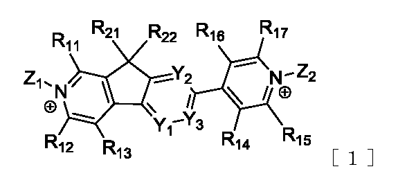
- One embodiment of the present invention provides an organic compound represented by the following general formula [1].
- Z 1 and Z 2 are each independently selected from an alkyl group which may have a substituent, an aryl group which may have a substituent, and an aralkyl group which may have a substituent. .
- R 11 to R 17 are each independently selected from a hydrogen atom and a substituent.
- the substituent may have an alkyl group which may have a substituent, an alkoxy group which may have a substituent, an aryl group which may have a substituent, or a substituent. It is either a heterocyclic group or a halogen atom.
- R 21 and R 22 are each independently selected from a hydrogen atom and a substituent.
- the substituent is an alkyl group which may have a substituent, an aryl group which may have a substituent, or an aralkyl group which may have a substituent.
- Y 1 to Y 3 are each independently selected from a carbon atom, an N atom, and (N + -L) (X ⁇ ).
- L is any of an alkyl group, an aryl group and an aralkyl group which may have a substituent.
- a cathodic electrochromic compound that absorbs light having a wavelength of 450 to 540 nm during coloring can be provided.
- FIG. 2 is a schematic diagram illustrating an example of a driving device connected to the electrochromic element according to the embodiment.
- FIG. 1 is a schematic diagram illustrating an example of an imaging device according to an embodiment.
- FIG. 1 is a schematic diagram illustrating an example of an imaging device according to an embodiment. It is a schematic diagram which shows an example of the window material which concerns on embodiment. It is a schematic diagram which shows an example of the window material which concerns on embodiment.
- FIG. 13 is a view showing a transmittance spectrum of Exemplified Compound A-20 in Example 7 in a decolored state and a colored state.
- 14 is an ultraviolet-visible absorption spectrum of the device produced in Example 11.
- 9 is a transmittance spectrum in a decolored state and a colored state (reduced state) of Exemplified Compound B-20.
- One embodiment of the present invention is an organic compound having electrochromic properties, which is an organic compound represented by the general formula [1].
- Z 1 and Z 2 are each independently an alkyl group which may have a substituent, an aryl group which may have a substituent, and an aralkyl group which may have a substituent.
- Z 1 and Z 2 are preferably an aryl group which may have a substituent.
- the aryl group may be, for example, a phenyl group or a naphthyl group, and preferably has an alkyl group as a substituent.
- This alkyl group may be substituted at the para-position to the basic skeleton of the general formula [1]. Further, the alkyl group may be substituted at the ortho position with respect to the basic skeleton of the general formula [1].
- the alkyl group is preferably an alkyl group having 1 to 8 carbon atoms.
- the basic skeleton refers to a structure in which Z 1 , Z 2 , R 11 to R 17 , R 21 and R 22 are all hydrogen atoms in the general formula [1].
- the organic compound according to one embodiment of the present invention may be present together with a counter ion.
- a counter ion Assuming that the counter ion is X ⁇ , it is represented by the following general formula [2].
- R 11 to R 17 are each independently selected from a hydrogen atom and a substituent.
- the substituent is an alkyl group which may have a substituent, an alkoxy group which may have a substituent, an aryl group which may have a substituent, a heterocyclic group which may have a substituent, or Any of halogen atoms.
- R 16 and R 17 may combine with each other to form a ring.
- R 21 and R 22 are each independently selected from a hydrogen atom and a substituent. These substituents are any of an alkyl group which may have a substituent, an aryl group which may have a substituent, and an aralkyl group which may have a substituent.
- Y 1 to Y 3 are each independently selected from a carbon atom, an N atom, and (N + -L) (X ⁇ ).
- L is any of an alkyl group, an aryl group and an aralkyl group which may have a substituent.
- Y 1 and Y 2 may be represented by an N atom or (N + -L) (X ⁇ ), and Y 3 may be a carbon atom. Further, Y 1 may be an N atom or (N + -L) (X ⁇ ), and the other two may be carbon atoms. Y 1 to Y 3 may be all carbon atoms.
- the alkyl group represented by Z 1 and Z 2 , R 11 to R 17 , R 21 and R 22 preferably has 1 to 8 carbon atoms, and may be linear, branched or cyclic. Further, a hydrogen atom may be replaced by a fluorine atom. Further, the carbon atom of the alkyl group may be replaced by an ester group or a cyano group.
- alkyl group examples include a methyl group, an ethyl group, a normal propyl group, an isopropyl group, a normal butyl group, a tertiary butyl group, an octyl group, a cyclohexyl group, and a trifluoromethyl group.
- the terminal of the alkyl group represented by Z 1 and Z 2 may have an adsorbing group for adsorbing to the porous electrode or an acid ester group thereof.
- the adsorptive group or its acid ester group include a carboxyl group and a carboxylester group, a sulfonic acid group and a sulfonic acid ester group, a phosphonic acid group and a phosphonic acid ester group, and a trialkoxysilyl group.
- the terminal of the alkyl group may have a polar group such as a hydroxyl group or an amino group, or an ionic group such as ammonium, pyridinium, and quinolinium.
- the aryl group represented by Z 1 and Z 2 , R 11 to R 17 , R 21 and R 22 is, for example, a phenyl group, a biphenyl group, a tolyl group, a fluorenyl group, a naphthyl group, a fluoranthenyl group, an anthryl group, Examples include a phenanthryl group, a pyrenyl group, and a perylenyl group. Preferably it is a phenyl group.
- aryl group (heterocyclic group) containing a hetero atom examples include a pyridyl group, a thienyl group, an oxazolyl group, an oxadiazolyl group, a thiazolyl group, a thiadiazolyl group, and an indolyl group.
- a pyridyl group Preferably it is a pyridyl group.
- the aryl group has a halogen atom, an alkyl group having 1 to 6 carbon atoms, an alkoxy group having 1 to 4 carbon atoms, an aryl group, an aralkyl group, a hydroxyl group, a substituted amino group, and a substituted silyl group as substituents. You may.
- the hydrogen atom of the alkyl group or the alkoxy group may be replaced by a halogen atom, preferably a fluorine atom.
- the aryl group represented by Z 1 and Z 2 has an alkyl group or an alkoxy group
- its terminal may have an adsorption group for adsorbing to the porous electrode or an acid ester group thereof, It may have an ionic group in order to improve solubility in an organic solvent.
- Adsorptive group or its ester group specific examples of the ionic group are the same as those mentioned in the alkyl groups represented by Z 1 and Z 2.
- the aralkyl group represented by Z 1 and Z 2 , R 21 and R 22 includes a benzyl group, a phenethyl group and the like.
- the aralkyl group may have a substituent, and specifically may have an alkyl group having 1 to 8 carbon atoms and an alkoxy group having 1 to 8 carbon atoms.
- the hydrogen atom of the alkyl group or the alkoxy group may be replaced by a halogen atom, preferably a fluorine atom.
- the aralkyl group represented by Z 1 and Z 2 has an alkyl group or an alkoxy group
- its terminal may have an adsorbing group for adsorbing to the porous electrode or an acid ester group thereof, It may have an ionic group in order to improve solubility in an organic solvent.
- Adsorptive group or its ester group specific examples of the ionic group are the same as those mentioned in the alkyl groups represented by Z 1 and Z 2.
- the alkoxy groups represented by R 11 to R 17 may be linear, branched, or cyclic. This alkoxy group preferably has 1 to 8 carbon atoms. Further, a hydrogen atom of the alkoxy group may be replaced by a halogen atom.
- a methoxy group, an ethoxy group and an isopropoxy group are particularly preferred.
- halogen atom represented by R 11 to R 17 examples include fluorine, chlorine, bromine, iodine, and the like.
- Y 1 to Y 3 are each independently selected from a carbon atom, an N atom, and (N + -L) (X ⁇ ).
- L is any of an alkyl group, an aryl group and an aralkyl group which may have a substituent. Specific examples of the alkyl group, aryl group and aralkyl group represented by L are the same as the examples of the alkyl group, aryl group and aralkyl group represented by Z 1 and Z 2 .
- anion represented by X ⁇ examples include anions such as PF 6 ⁇ , ClO 4 ⁇ , BF 4 ⁇ , AsF 6 ⁇ , SbF 6 ⁇ , CF 3 SO 3 ⁇ , and (CF 3 SO 2 ) 2 N ⁇ . It is selected from halogen anions such as Br ⁇ , Cl ⁇ and I ⁇ . Preferably PF 6 -, ClO 4 -, BF 4 -, CF 3 SO 3 -, (CF 3 SO 2) 2 N - is either. When a plurality of X - are included, they may be the same or different.
- the method for producing the organic compound according to one embodiment of the present invention is not particularly limited, but for example, it can be produced by the following method.
- Z 1 and Z 2 are an alkyl group and an aralkyl group
- the compound represented by the general formula [1] is reacted with an organic compound represented by the following general formula [2] and a halide in a predetermined solvent.
- an anion exchange reaction can be performed with a salt containing a desired anion in a predetermined solvent.
- Z 1 and Z 2 are aryl groups
- an organic compound represented by the general formula [3] is reacted with 2,4-dinitrophenyl halide, and X 1 and X 2 are 2,4-dinitrophenyl groups.
- the compound can be reacted with an arylamine and subjected to an anion exchange reaction with a salt containing an anion in a predetermined solvent.
- an anion exchange reaction with a salt containing an anion in a predetermined solvent.
- a solvent and a reaction temperature only one imine can be reacted. By repeating the reaction, it is also possible to introduce different substituents into two imines.
- the production method of the general formula [3] is not particularly limited, but for example, it can be produced according to the following production method as an example.
- Intermediate 1 can be synthesized by coupling an N, N-diethylnicotinamide derivative with a 4-halogeno-pyridylpyridine derivative.
- the intermediate 2 can be synthesized by cyclizing the intermediate 1 using LDA (lithium diisopropylamide).
- intermediate 3 can be synthesized by reducing Wolff-Kishner intermediate 2.
- the organic compound represented by the general formula [3] can be synthesized by reacting the intermediate 3 with a desired alkyl halide in the presence of a base.
- Y 1 to Y 3 are each independently selected from a carbon atom, an N atom, and (N + -L) (X ⁇ ). In any case, the compound can be synthesized by the above reaction route.
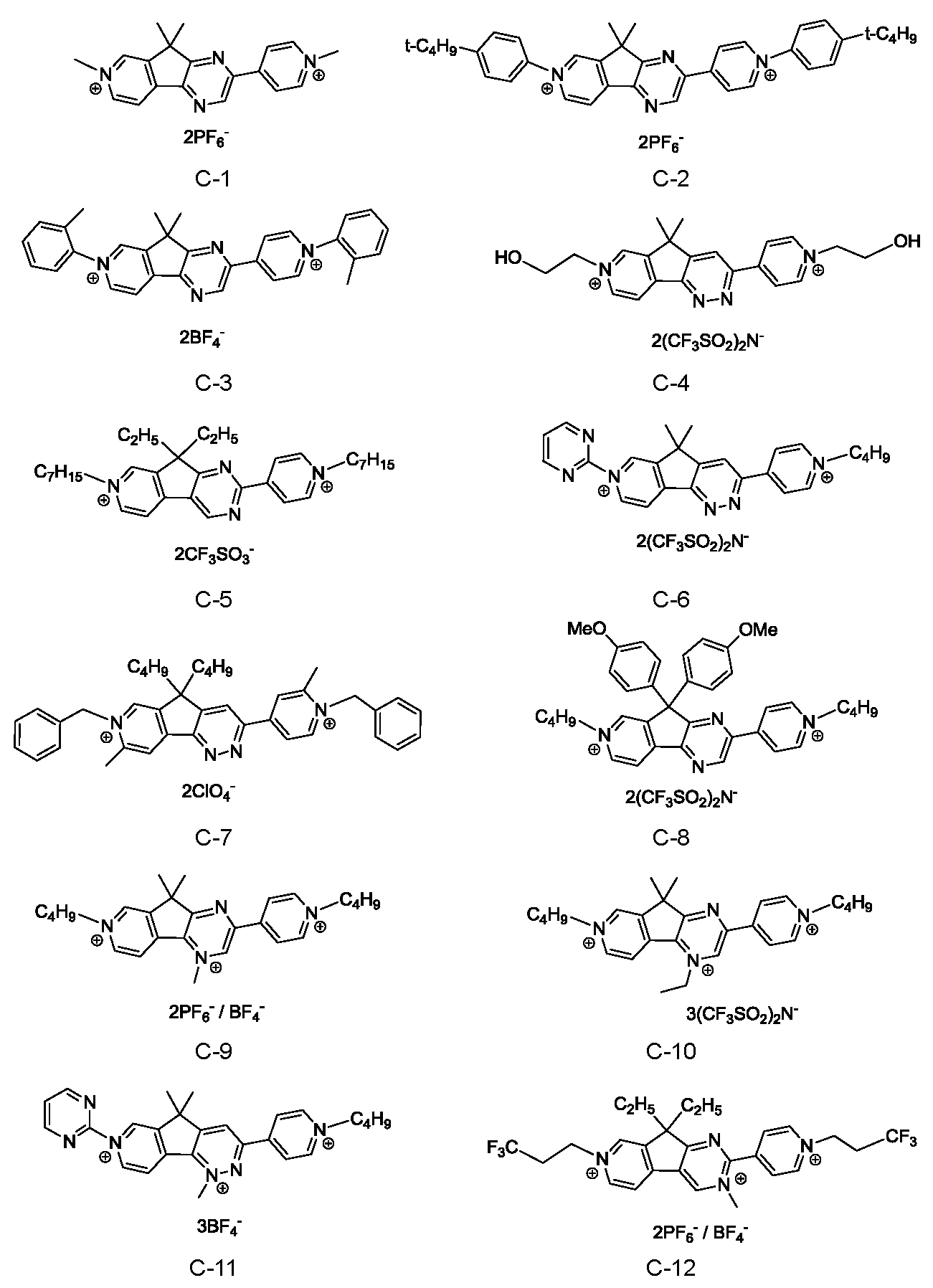
- Compounds shown in Group A among the exemplified compounds are compounds in which Y 1 to Y 3 in the general formula [1] are all carbon atoms.
- one of Y 1 to Y 3 in the general formula [1] is represented by N atom or (N + -L) (X ⁇ ), and the remaining two are carbon atoms. It is a structure consisting of
- the organic compound represented by the general formula [1] is a cathodic EC compound that is colored in a reduced state. That is, the organic compound represented by the general formula [1] is a compound whose properties of optical absorption (coloration state and light transmittance) change due to reversible electrochemical redox reaction. .
- the organic compound according to one embodiment of the present invention has the structure represented by the general formula [1], it can absorb light having a wavelength of 450 to 540 nm during coloring.
- the compound preferably has a low LUMO (lowest unoccupied orbital) level.
- a low LUMO level can mean that the LUMO level is deep, farther from the vacuum level, and that the absolute value of LUMO is large.
- the cathodic EC compound represented by the general formula [1] includes a heterocyclic ring in which a central aromatic ring connecting two pyridine rings contains an N atom. For this reason, the electron density is reduced, and the LUMO is stabilized (deep), so that electrons can be easily injected, that is, the reduction potential shifts in the positive direction.
- the organic compounds (B-4, B-20, B-21) and (C-1, C-2, C-2) according to an embodiment of the present invention are compared.
- -3) and Reference Example Compounds (Ref-1, Ref-2, Ref-3) were verified by molecular orbital calculation.
- Compounds (B-4, B-20, B-21) have a single pyridine ring in which the N atom of the central aromatic ring is one, and compounds (C-1, C-2, C-3) have a central aromatic ring.
- the N atom of the aromatic ring is two pyrazine rings.
- the comparative compounds (Ref-1, Ref-2, Ref-3) are benzene rings in which the central aromatic ring does not contain an N atom, and the other chemical structures are the same as those of the organic compound according to one embodiment of the present invention ( B-4, B-20, B-21) and (C-1, C-2, C-3).
- the reduction potentials determined from the molecular orbital calculations are summarized in Tables 1 to 3 below.
- the reduction potentials of the compounds (B-4, B-20, B-21) and (C-1, C-2, C-3) according to one embodiment of the present invention are as follows. In each case, it was confirmed that the positive potential was shifted from the reduction potential of the reference compound (Ref-1, Ref-2, Ref-3).
- the organic compound according to one embodiment of the present invention can contribute to lowering the voltage of the EC device than the reference compound.
- the molecular orbital calculation was performed using Gaussian 03 * Revision D. This is a result of performing a ground state structure optimization calculation using 01. At that time, Density Functional Theory was adopted as a quantum chemical calculation method, and B3LYP was used as a functional.
- the basis functions are Gaussian 03, Revision D. In 01, 6-31G * was used.
- the organic compound according to one embodiment of the present invention can be used as an EC layer of an electrochromic device.
- the EC device shown in FIG. 1 is an EC device having a pair of transparent electrodes 11 and an EC layer 12 having an electrolyte and an EC organic compound according to the present invention disposed between the pair of electrodes.
- the distance between the electrodes of the pair of electrodes is fixed by the sealing material 13.
- a pair of electrodes is arranged between a pair of transparent substrates 10.
- the EC layer 12 has the organic compound according to the present invention.
- the EC layer may have a layer made of an EC compound and a layer made of an electrolyte. Further, an EC layer may be provided as a solution containing an EC compound and an electrolyte.
- the EC device according to the present embodiment is preferably an EC device in which the EC layer is a solution layer.
- the electrolyte is not limited as long as it is an ion-dissociable salt, has good solubility in a solvent, and shows high compatibility in a solid electrolyte. Among them, an electrolyte having an electron donating property is preferable. These electrolytes can also be called supporting electrolytes.
- electrolyte examples include inorganic ion salts such as various alkali metal salts and alkaline earth metal salts, and quaternary ammonium salts and cyclic quaternary ammonium salts.
- the solvent for dissolving the EC organic compound and the electrolyte is not particularly limited as long as the solvent can dissolve the EC organic compound and the electrolyte, but a polar solvent is particularly preferable.
- the EC medium may further contain a polymer or a gelling agent to use a highly viscous one or a gelled one.
- These polymers and gelling agents can also be called thickeners.
- the EC solution preferably has a thickener.
- the viscosity of the EC solution may be between 10 and 5000 cP, and between 50 and 1000 cP.
- the viscosity of the EC solution may be 150 cP or less, preferably 100 cP or less, more preferably 65 cP or less. Further, the viscosity of the EC solution may be 20 cP or more, preferably 50 cP or more.
- the thickener may have a weight ratio of 20 wt% or less when the weight of the electrochromic layer is 100 wt%. Preferably it is 1 wt% or more and 15 wt% or less, more preferably 5 wt% or more and 10 wt% or less.
- the polymer is not particularly limited and includes, for example, polyacrylonitrile, carboxymethylcellulose, polyvinyl chloride, polyethylene oxide, polypropylene oxide, polyurethane, polyacrylate, polymethacrylate, polyamide, polyacrylamide, polyester, Nafion (registered trademark) and the like.
- polyacrylonitrile carboxymethylcellulose
- polyvinyl chloride polyethylene oxide
- polypropylene oxide polyurethane
- polyacrylate polymethacrylate
- polyamide polyacrylamide
- polyester Nafion (registered trademark) and the like.
- the transparent substrate and the transparent electrode will be described.
- the transparent substrate 10 for example, a colorless or colored glass, a tempered glass, or the like, or a colorless or colored transparent resin is used.
- “transparent” indicates that the visible light transmittance is 70% or more.
- polyethylene terephthalate polyethylene naphthalate, polynorbornene, polyamide, polysulfone, polyethersulfone, polyetheretherketone, polyphenylenesulfide, polycarbonate, polyimide, polymethylmethacrylate, and the like can be given.
- Examples of the electrode material 11 include indium tin oxide alloy (ITO), fluorine-doped tin oxide (FTO), tin oxide (NESA), indium zinc oxide (IZO), silver oxide, vanadium oxide, molybdenum oxide, gold, silver,
- ITO indium tin oxide alloy
- FTO fluorine-doped tin oxide
- NESA tin oxide
- IZO indium zinc oxide
- silver oxide vanadium oxide, molybdenum oxide
- gold silver
- Examples include metals such as platinum, copper, indium, and chromium, metal oxides, silicon-based materials such as polycrystalline silicon and amorphous silicon, and carbon materials such as carbon black, graphite, and glassy carbon.
- a conductive polymer whose conductivity is improved by doping treatment or the like for example, polyaniline, polypyrrole, polythiophene, polyacetylene, polyparaphenylene, a complex of polyethylenedioxythiophene (PEDOT) and polystyrenesulfonic acid, and the like are suitably used.
- PEDOT polyethylenedioxythiophene
- the sealing material 13 is preferably used to hold the EC layer between the pair of electrodes and to keep the distance between the electrodes.
- the sealing material 13 may have a function of maintaining the distance between the electrodes by, for example, containing a spacer material.
- the sealing material 13 is disposed between the pair of electrodes 11 and provides a space for accommodating the solution 12 having the EC organic compound of the present invention.
- the sealing material 13 is preferably a material that is chemically stable, hardly permeates gas and liquid, and does not inhibit the oxidation-reduction reaction of the EC compound.
- an inorganic material such as a glass frit, a thermosetting or photocurable material such as an epoxy resin or an acrylic resin, polyimide, polytetrafluoroethylene, and fluororubber can be used.
- the EC element according to the present embodiment may have a liquid injection port formed by a pair of electrodes and a spacer. After enclosing the composition having the EC organic compound from the liquid injection port, the injection port is covered with a sealing member, and further sealed with an adhesive or the like to obtain an element.
- the sealing member also has a role of isolating the adhesive and the EC organic compound so as not to come into contact with each other.
- the method for forming the EC element according to this embodiment is not particularly limited, and a liquid containing an EC organic compound prepared in advance by a vacuum injection method, an air injection method, a meniscus method, or the like in a gap provided between a pair of electrodes. 12 can be used.
- Each of the pair of electrodes may be an electrode substrate in which the electrode and the substrate are integrated.
- the EC device 1 may include the organic compound according to the present invention and a second organic compound different from the organic compound.
- the second organic compound may be one type or a plurality of types, and may be an anodic EC compound that is colored in an oxidized state, a cathodic EC compound that is colored in a reduced state, or a compound having both properties. Since the organic compound according to the present invention is a compound that is colored in a reduced state, the second organic compound is preferably an anodic EC compound that is colored in an oxidized state.
- the electrochromic layer may have a structure in which the absorption spectrum is made nearly flat by having four or more kinds of electrochromic compounds.
- the anodic EC compound that is colored in an oxidized state is a compound having a visible light transmittance in an oxidized state lower than that in a reduced state. It is sufficient that the transmittance of any of the visible light regions is changed, and the transmittance of the entire visible light region does not need to be changed.
- a third organic compound may be further contained.
- the third organic compound may be an anodic EC compound or a cathodic EC compound.
- the absorption wavelength region of other EC compounds when decoloring is preferably 400 nm or less when decoloring. This is because an element having high transparency at the time of decoloring can be provided.
- the absorption wavelength range during coloring is preferably in the range of 400 nm to 800 nm, more preferably 400 nm to 450 nm, or 600 nm to 700 nm.
- an EC element having another EC compound absorbs light in the visible light region uniformly at each wavelength.
- EC compounds according to the present embodiment include, for example, compounds having the following structural formula.
- EC compounds that color in an oxidized state include oligothiophenes, phenazine-based compounds such as 5,10-dihydro-5,10-dimethylphenazine, 5,10-dihydro-5,10-diisopropylphenazine, ferrocene, and tetraphenylene.
- Metallocene compounds such as -t-butylferrocene and titanocene
- phenylenediamine compounds such as N, N ', N, N'-tetramethyl-p-phenylenediamine
- pyrazoline compounds such as 1-phenyl-2-pyrazoline, etc. Is mentioned.
- Compounds that are colored in the reduced state include N, N′-diheptylbipyridinium diperchlorate, N, N′-diheptylbipyridinium ditetrafluoroborate, N, N′-diheptylbipyridinium dihexafluorophosphate, N, N '-Diethylbipyridinium diperchlorate, N, N'-diethylbipyridinium ditetrafluoroborate, N, N'-diethylbipyridinium dihexafluorophosphate, N, N'-dibenzylbipyridinium diperchlorate, N, N'-di Benzylbipyridinium ditetrafluoroborate, N, N'-dibenzylbipyridinium dihexafluorophosphate, N, N'-diphenylbipyridinium diperchlorate, N, N'
- the phenazine-based compound is a compound having a 5,10-dihydro-phenazine skeleton in a chemical structure.
- Phenazine-based compounds include compounds having a substituent on 5,10-dihydrophenazine.
- the hydrogen atoms at positions 5 and 10 of 5,10-dihydrophenazine may be substituted with an alkyl group such as a methyl group, an ethyl group, or a propyl group, or an aryl group such as a phenyl group.
- the phenazine-based compound may be a compound having an alkyl group having 1 to 20 carbon atoms in 5,10-dihydrophenazine. Further, a compound having an alkoxy group having 1 to 20 carbon atoms in 5,10-dihydrophenazine may be used. Further, a compound having an aryl group having 4 to 60 carbon atoms in 5,10-dihydrophenazine may be used. The same applies to other compounds, for example, viologen compounds.
- the compound contained in the EC layer 12 of the EC device 1 according to the present embodiment can be confirmed to be contained in the EC device 1 by extracting and analyzing the compound by a known method. For example, extraction by chromatography and analysis by NMR can be mentioned. When the electrochromic layer is a solid, it can be analyzed by TOF-SIMS or the like.
- the EC device according to the present embodiment has high transparency at the time of decoloring, gives high optical density at the time of coloring, and can reduce the transmittance, and greatly reduces the amount of light incident on an imaging device such as a camera. It can be suitably used when performing.
- the EC element 1 according to the present embodiment can be used for an optical filter, a lens unit, an imaging device, a window material, and the like. Further, by providing the EC element according to the present embodiment and the light reflecting member having the EC element on the light reflecting surface, an electrochromic mirror can be obtained.
- the light reflecting member may also serve as an electrode and a substrate.
- the optical filter according to one embodiment of the present invention has an EC element 1 and an active element connected to the EC element 1.
- the active element is an active element that drives the electrochromic element and adjusts the amount of light passing through the electrochromic element.
- Examples of the active element include a transistor and an MIM element.
- the transistor may include an oxide semiconductor such as InGaZnO in the active region.
- the optical filter has the EC device 1 according to the present embodiment and a driving device connected to the EC device 1.
- FIG. 2 is a schematic diagram illustrating an example of the driving device 20 of the EC device 1 and the EC device 1 driven by the driving device 20.
- the drive device 20 for the EC element 1 according to the present embodiment includes a drive power supply 8, a resistance switch 9, and a controller 7.
- the drive power supply 8 applies a voltage necessary for the EC material included in the EC layer 12 to cause an electrochemical reaction to the EC element 1.
- a method suitable for the element to be used is adopted. More specifically, a method of inputting a predetermined condition to the EC element 1 with respect to a desired transmittance setting value, or a setting value by comparing the transmittance setting value with the transmittance of the EC element 1 There is a method of selecting and inputting a condition so as to match a value.
- the parameters to be changed include a voltage, a current, and a duty ratio.
- the controller 7 increases or decreases the voltage for the voltage control method, the current for the current control method, or the duty ratio for the pulse width modulation method to the EC element 1, thereby increasing or decreasing the corresponding EC.
- the coloring density of the device can be increased or decreased, and consequently the incident light can be reduced or increased.
- the resistance switch 9 switches between a resistor R1 (not shown) and a resistor R2 larger than the resistor R1 in a closed circuit including the drive power supply 8 and the EC element 1, and connects them in series.
- the resistance value of the resistor R1 is preferably at least smaller than the largest impedance of the element closed circuit, and is preferably 10 ⁇ or less.
- the resistance value of the resistor R2 is preferably larger than the largest impedance of the element closed circuit, and is preferably 1 M ⁇ or more.
- the resistor R2 may be air. In this case, the closed circuit is strictly an open circuit, but it can be considered as a closed circuit by regarding the air as the resistance R2.
- the controller 7 sends a switching signal to the resistance switch 9 to control the switching between the resistors R1 and R2.
- the lens unit according to the present embodiment has a plurality of lenses and an optical filter having the EC element 1.
- the optical filter may be provided between the plurality of lenses or outside the lenses.
- the optical filter is preferably provided on the optical axis of the lens.
- the imaging device includes an optical filter and a light receiving element that receives light that has passed through the optical filter.
- the imaging device include a camera, a video camera, a camera-equipped mobile phone, and the like.
- the imaging device may have a form in which a main body having a light receiving element and a lens unit having a lens can be separated.
- the imaging device when the imaging device can be separated by the main body and the lens unit, a mode in which an optical filter separate from the imaging device is used at the time of imaging is also included in the present invention.
- the arrangement position of the optical filter includes the outside of the lens unit, between the lens unit and the light receiving element, between a plurality of lenses (when the lens unit has a plurality of lenses), and the like.
- FIG. 3 is a schematic diagram illustrating an example of a configuration of an imaging device 100 using the optical filter of the present embodiment.
- the imaging device 100 is an imaging device including the lens unit 102 and the imaging unit 103.
- the lens unit 102 includes the optical filter 101 and an imaging optical system having a plurality of lenses or lens groups.
- the optical filter 101 is the above-described optical filter of the present embodiment.
- the lens unit 102 represents, for example, a rear focus type zoom lens that performs focusing after the stop in FIG. 3A.
- a first lens group 104 having a positive refractive power In order from the object side, a first lens group 104 having a positive refractive power, a second lens group 105 having a negative refractive power, a third lens group 106 having a positive refractive power, and a fourth lens group having a positive refractive power It has 107 lens groups. Zooming is performed by changing the distance between the second lens group 105 and the third lens group 106, and focusing is performed by moving a part of the fourth lens group 107.
- the lens unit 102 has, for example, an aperture stop 108 between the second lens group 105 and the third lens group 106, and has an aperture stop 108 between the third lens group 106 and the fourth lens group 107. It has an optical filter 101.
- the light passing through the lens unit is arranged so as to pass through each of the lens groups 104 to 107, the stop 108, and the optical filter 101, so that the light amount can be adjusted using the aperture stop 108 and the optical filter 101.
- the lens unit 102 is detachably connected to the imaging unit 103 via a mount member (not shown).
- the optical filter 101 is disposed between the third lens group 106 and the fourth lens group 107 in the lens unit 101, but the imaging device 100 is not limited to this configuration.
- the optical filter 101 may be located either before (subject side) or after the aperture stop 108 (on the imaging unit 103 side), or before any of the first to fourth lens groups 104 to 107. Later, it may be between the lens groups. If the optical filter 101 is arranged at a position where light converges, there is an advantage that the area of the optical filter 101 can be reduced.
- the configuration of the lens unit 102 is not limited to the above-described configuration, and can be appropriately selected.
- an inner focus type in which focusing is performed before the stop may be used, or another type may be used.
- a special lens such as a fisheye lens or a macro lens can be appropriately selected.
- the imaging unit 103 has a glass block 109 and a light receiving element 110.
- the glass block 109 is a glass block such as a low-pass filter, a face plate, and a color filter.
- the light receiving element 110 is a sensor unit that receives light that has passed through the lens unit, and an imaging element such as a CCD or a CMOS can be used. Also, an optical sensor such as a photodiode may be used, and a sensor that acquires and outputs information on light intensity or wavelength may be used as appropriate.
- the driving device may be arranged inside the lens unit 102 or outside the lens unit 102.
- the drive is controlled by connecting the EC device 1 in the lens unit 102 and the driving device through wiring.
- the optical filter 101 is disposed inside the lens unit 102.
- the present invention is not limited to this mode, and the optical filter 101 may be arranged at an appropriate location inside the imaging device 100, and the light receiving element 110 may be arranged to receive light passing through the optical filter 101.
- FIG. 3B is a schematic diagram of an example of an imaging device in which an optical filter is arranged in the imaging device.
- the imaging unit 103 has the optical filter 101.
- the optical filter 101 is disposed immediately before the light receiving element 110.
- the lens unit 102 to be connected does not have to have the optical filter 101, so that a dimmable imaging device using the existing lens unit 102 can be configured. It becomes possible.
- the imaging device 100 of the present embodiment is applicable to a product having a combination of light quantity adjustment and a light receiving element.
- a camera can be used for a camera, a digital camera, a video camera, a digital video camera, and also applicable to a product having a built-in imaging device such as a mobile phone, a smartphone, a PC, and a tablet.
- FIG. 4A is a schematic view showing a window using the EC element 1 according to the present embodiment
- FIG. 4B is a schematic view showing a cross-sectional view taken along line X-X ′ of FIG. 4A.
- the light control window 111 of the present invention includes the EC element 1 (optical filter), a transparent plate 113 sandwiching the EC element 1, and a frame 112 that surrounds and integrates the whole.
- the optical filter has a driving device (not shown), and the driving device may be integrated in the frame 112 or may be arranged outside the frame 112 and connected to the EC element 1 through wiring.
- the transparent plate 113 is not particularly limited as long as it has a high light transmittance, and is preferably a glass material in consideration of use as a window.
- the material of the frame 112 is not limited, but a resin such as polycarbonate, acrylonitrile butadiene styrene, polyalkylene furandicarboxylate, polylactic acid, polybutadiene terephthalate, or a mixture thereof may be used.
- a resin such as polycarbonate, acrylonitrile butadiene styrene, polyalkylene furandicarboxylate, polylactic acid, polybutadiene terephthalate, or a mixture thereof may be used.
- the frame may be any frame that covers at least a part of the optical filter and has an integrated form.
- the EC element 1 is a component independent of the transparent plate 113.
- the transparent substrate 10 of the EC element 1 may be regarded as the transparent plate 113.
- Such a dimming window can be applied, for example, to an application for adjusting the amount of daylight sunlight entering a room. Since the present invention can be applied not only to the adjustment of the amount of heat but also the amount of heat of the sun, it can be used for controlling the brightness and temperature of a room. Also, the shutter can be applied to an application that blocks a view from the outside to the room. Such a light control window can be applied to a window of a vehicle such as an automobile, a train, an airplane, and a ship, in addition to a glass window for a building.
- the electrochromic device may be used for an electrochromic mirror provided on a moving body such as an automobile.
- the electrochromic mirror has a light reflecting member that reflects light dropped on the electrochromic element.
- the EC element 1 including the organic compound represented by the general formula [1] in the EC layer 12 can be used for an optical filter, a lens unit, an imaging device, a window material, and the like.
- Each of the optical filter, the lens unit, the imaging device, and the window material of the present embodiment can be variously formed by combining the organic compound represented by the general formula [1] alone or an EC compound having colored absorption in another wavelength band. It is possible to provide an excellent absorption color.
- the imaging device 100 of the present embodiment by using the optical filter 101 as a light control member, it is possible to appropriately change the light control amount with a single filter, thereby reducing the number of members and saving space. There are advantages.
- reaction solution was added to saturated aqueous sodium hydrogen carbonate, extracted with ethyl acetate, the organic layers were combined, washed sequentially with water and saturated saline, dried over anhydrous sodium sulfate and concentrated to obtain a black-yellow solid.
- N, N-diethylnicotinamide (5.35 g, 30 mmol), triisopropyl borate (7.6 ml, 33 mmol) and tetrahydrofuran (25 ml) were charged and cooled to -50 ° C.
- the previously prepared LDA solution was slowly dropped, and the mixture was stirred at 0 ° C. for 2 hours and concentrated under reduced pressure.
- XX-1 (4.72 g, 30 mmol)
- potassium phosphate (10.73 g, 75 mmol)
- 1,4-dioxane / pure water 150 ml / 45 ml
- Exemplified compound B-3 (261 mg, 0.41 mmol) was dissolved in water. An aqueous solution in which 320 mg of ammonium hexafluorophosphate was dissolved was added dropwise, and the mixture was stirred at room temperature for 3 hours. The precipitated crystals were filtered and washed successively with water, isopropyl alcohol, and diethyl ether to obtain 235 mg (yield: 85%) of Exemplified Compound B-4.
- Exemplified compound B-4 (205 mg, 0.30 mmol) and dichloromethane (6 ml) were added to the reaction vessel, and further trimethyloxonium tetrafluoroborate (444 mg, 3.0 mmol) was added, followed by stirring at room temperature for 2 days. The precipitated solid was filtered and washed sequentially with dichloromethane, methanol and diethyl ether to obtain 75 mg of Exemplified Compound B-34 (yield: 30%).
- Example 8 ⁇ Synthesis of Exemplified Compound B-6> XX-5 (104 mg, 0.38 mmol) synthesized in Example 5, bromoacetonitrile (228 mg, 1.90 mmol), and 4 ml of acetonitrile were added to the reaction vessel, and the mixture was heated at 90 ° C. and refluxed for 20 hours. . After completion of the reaction, the precipitated crystals were filtered and washed with ethyl acetate to obtain Exemplified Compound B-6 (140 mg, yield: 72%).
- Exemplified Compound B-6 (140 mg, 0.27 mmol) was dissolved in 10 ml of water. An aqueous solution in which 160 mg of ammonium hexafluorophosphate was dissolved was added dropwise, and the mixture was stirred at room temperature for 3 hours. The precipitated crystals were filtered and washed successively with water, isopropyl alcohol and diethyl ether to obtain 120 mg of Exemplified Compound B-7 (yield: 69%). The structure of this compound was confirmed by NMR measurement.
- Example 11 ⁇ Production of electrochromic device and evaluation of characteristics> As an electrolyte, tetrabutylammonium perchlorate was dissolved in propylene carbonate at a concentration of 0.1 M, and then Exemplified Compound A-20 of Example 2 was dissolved at a concentration of 40.0 mM to obtain an EC medium.
- an insulating layer SiO 2
- ITO transparent conductive films
- a PET film (Melinex S (registered trademark, manufactured by Teijin DuPont Films, Inc., 125 ⁇ m thickness) that defines the substrate interval) was disposed between a pair of glass substrates with a transparent electrode film. Thereafter, the substrate and the PET film were bonded and sealed with an epoxy-based adhesive leaving an injection port for injecting the EC medium. As described above, an empty cell with an inlet was produced.
- the EC medium obtained above was injected from the above-described injection port by a vacuum injection method, and the injection port was sealed with an epoxy-based adhesive to obtain an EC element.
- the EC device immediately after fabrication exhibited a transmittance of about 80% over the entire visible light region, and had high transparency.
- FIG. 5 is an ultraviolet-visible absorption spectrum of the device manufactured in Example 10.
- a light source a DH-2000S deuterium, halogen light source manufactured by Ocean Optics was used.
- Example 12 ⁇ Production of electrochromic device and evaluation of characteristics> A device was prepared in the same manner as in Example 11, except that Exemplified Compound A-18 was used instead of Exemplified Compound A-20.
- FIG. 6 is an ultraviolet-visible absorption spectrum of the device produced in Example 12.
- the measurement was performed using a solution in which the exemplified compound B-20 was dissolved (2.0 ⁇ 10 ⁇ 3 mol / L) in a propylene carbonate solution (0.1 mol / L) of tetrabutylammonium hexafluorophosphate as a supporting electrolyte. I went. This solution is placed in a glass cell having an optical path length of 1 mm, a mesh-shaped platinum electrode (working electrode) and a wire-shaped platinum electrode (counter electrode) are arranged, and a reference electrode RE (Ag / Ag + ) is arranged and measured. Was done.
- the transmittance spectrum was measured using a transmitted light passing through a mesh electrode by performing a constant potential reduction on the solution at a reduction potential of the compound or higher.
- a voltage was applied using a potentiostat (Cell Test 1470E) manufactured by Solartron, and a spectrometer (USB2000-UV-VIS) manufactured by Ocean Optics was used for spectroscopic measurement.
- FIG. 7 shows transmittance spectra of Exemplified Compound B-20 in a decolored state and a colored state (reduced state).
- Exemplified compound B-20 is a material having high transparency without absorption in the entire visible light region in the decolored state.
- the transmittance changed in the visible region, and the wavelength ⁇ max of the absorption peak was 528 nm. This reduced coloring state returned to colorless and transparent again by oxidation, and reversible electrochromic characteristics associated with oxidation and reduction were confirmed.
- the cathodic EC compound Ref-2 of the reference example is a compound having the same chemical structure except that the central pyridine ring of the exemplified compound B-20 is a benzene ring.
- Ref-2 shows almost the same colored absorption wavelength ( ⁇ max to 536 nm) as the cathodic EC compound B-20 in the reduced state, but has a reduction potential of ⁇ 1.14 V, and is 150 mV more negative than the exemplary compound B-20. The reduction potential was indicated.
- Table 4 The results are summarized in Table 4.
- Example 14 ⁇ Evaluation of electrochromic characteristics> The measurement was carried out in the same manner as in Example 13, except that Exemplified Compound B-7 was used instead of Exemplified Compound B-20. The results are summarized in Table 4.
- Example 15 ⁇ Evaluation of electrochromic characteristics> The measurement was carried out in the same manner as in Example 13, except that Exemplified Compound B-34 was used instead of Exemplified Compound B-20. The results are summarized in Table 4.
- Example 16 ⁇ Evaluation of electrochromic characteristics> The measurement was carried out in the same manner as in Example 13, except that Exemplified Compound B-4 was used instead of Exemplified Compound B-20. The results are summarized in Table 4.
- Example 17 ⁇ Preparation of electrochromic device and evaluation of characteristics>
- Exemplified compound B-20 as a cathodic EC material and W-1 (5,10-diisopropyl-5,10-dihydrophenazine) having the following structure as an anodic EC material were dissolved in propylene carbonate at a concentration of 100 mM, respectively, and further increased.
- An EC solution was prepared by adding 5 wt% of polymethyl methacrylate (PMMA) as a viscosity agent.
- PMMA polymethyl methacrylate
- two transparent conductive glasses on which an indium-doped tin oxide (ITO) film was formed were prepared, and arranged so that the ITO films faced each other.
- the outer peripheries of the two transparent conductive glasses were bonded together using an epoxy-based sealing material in which spacer beads having a particle size of 50 ⁇ m were mixed.
- a solution in which the anodic EC compound and the cathodic EC compound are dissolved is injected into the transparent conductive glass from an injection port formed in advance, so that the space formed by the two sheets of the transparent conductive glass and the sealing material is formed. was filled with the solution. Thereafter, the injection port was sealed with a UV-curable sealant to obtain an EC element.
- the organic compound according to one embodiment of the present invention is a cathodic electrochromic compound that absorbs light having a wavelength of 450 to 540 nm when colored.
- the present invention can be used for an EC element that absorbs light in this region, an optical filter using the same, a lens unit, an imaging device, and the like.
Landscapes
- Chemical & Material Sciences (AREA)
- Organic Chemistry (AREA)
- Physics & Mathematics (AREA)
- Engineering & Computer Science (AREA)
- Structural Engineering (AREA)
- Nonlinear Science (AREA)
- Architecture (AREA)
- Civil Engineering (AREA)
- General Physics & Mathematics (AREA)
- Optics & Photonics (AREA)
- Electrochromic Elements, Electrophoresis, Or Variable Reflection Or Absorption Elements (AREA)
Abstract
本開示は、下記一般式[1]で表されることを特徴とする有機化合物を提供する。式中、Z1およびZ2は置換基を有してもよいアルキル基、置換基を有してもよいアリール基および置換基を有してもよいアラルキル基からそれぞれ独立に選ばれる。R11乃至R17、R21およびR22は、水素原子または置換基からそれぞれ独立に選ばれる。Y1乃至Y3は、炭素原子、N原子、または(N+-L)(X-)からそれぞれ独立に選ばれる。Lはアルキル基、アリール基、アラルキル基のいずれかである。
Description
本発明は、エレクトロクロミック性の有機化合物およびそれを有するエレクトロクロミック素子、光学フィルタ、レンズユニット、撮像素子及び窓に関する。
電気化学的な酸化還元反応により、物質の光学吸収の性質(呈色状態や光透過度)が変化するエレクトロクロミック(以下「EC」と省略する場合がある)材料としては無機材料、有機高分子材料、有機低分子材料など種々の材料が知られている。
有機低分子のEC材料の代表例としては、還元により着色する(カソード性化合物)ビオロゲン誘導体や、酸化により着色する(アノード性化合物)オリゴチオフェン誘導体等が挙げられる。
従来においては、EC素子の応用として自動車の調光ミラーや電子ペーパー等などが提案されている。これらのEC素子は、材料の選択によって多様な色調の表示が可能であるという特性を利用している。すなわち、多様な色調の材料を開発することが広汎な用途への展開が可能であることを示唆している。例えばフルカラーディスプレイ等への応用を考えた場合にはシアン、マゼンタ、イエローに着色する材料が必要となる。さらに広汎な用途への応用を考えた場合、着色時に多様な吸収波長を有するEC材料が必要になるため、分子設計による多様な色設計が可能な有機EC材料が注目されている。
エレクトロクロミック化合物を用いて、可視光領域の広い範囲を吸収するデバイスを構成するためには、様々な波長の光を吸収するために、様々なエレクトロクロミック化合物が求められている。
特許文献1には、2つのピリジン環の間にベンゼン環が結合した下記構造式C-1の有機化合物が還元着色時に570nmに光吸収を有することが記載されている。特許文献2には、下記構造式C-2の有機化合物が還元着色時に470nm近傍に光吸収を有することが記載されている。

特許文献1および特許文献2に記載されているエレクトロクロミック化合物は、着色時に570nmの波長の光を吸収する化合物、600nmの波長の光を吸収する化合物が記載されている。着色時の吸収波長域を変化させる手法の1つとしては、化学構造のビピリジニウム塩骨格の共役構造を変化させるため、環構造を増減させる手法が挙げられる。しかし、単に環構造を増減させるのみでは、450-540nmに吸収を有するエレクトロクロミック化合物は得られていなかった。
本発明は、上述の課題を鑑みてなされたものであり、着色時に450-540nmの波長の光を吸収するカソード性のエレクトロクロミック化合物を提供することを目的とする。
本発明の一実施形態は、下記一般式[1]で示されることを特徴とする有機化合物を提供する。
式中、Z1およびZ2は置換基を有してもよいアルキル基、または置換基を有していてもよいアリール基、置換基を有していてもよいアラルキル基からそれぞれ独立に選ばれる。
R11乃至R17は、水素原子または置換基からそれぞれ独立に選ばれる。前記置換基は、置換基を有していてもよいアルキル基、置換基を有していてもよいアルコキシ基、置換基を有していてもよいアリール基、置換基を有していてもよい複素環基又はハロゲン原子のいずれかである。R21及びR22は、水素原子または置換基からそれぞれ独立に選ばれる。前記置換基は、置換基を有していていもよいアルキル基、置換基を有していてもよいアリール基又は置換基を有していてもよいアラルキル基のいずれかである。
Y1乃至Y3は、炭素原子、N原子、または(N+-L)(X-)からそれぞれ独立に選ばれる。Lは置換基を有していてもよいアルキル基、アリール基、アラルキル基のいずれかである。
本発明によれば、着色時に450-540nmの波長の光を吸収するカソード性のエレクトロクロミック化合物を提供できる。
本発明の一実施形態は、エレクトロクロミック特性を有する有機化合物であり、一般式[1]で示される有機化合物である。

一般式[1]における、Z1およびZ2は置換基を有してもよいアルキル基、または置換基を有してもよいアリール基、置換基を有してもよいアラルキル基からそれぞれ独立に選ばれる。Z1およびZ2は、置換基を有してもよいアリール基であることが好ましい。当該アリール基は、例えば、フェニル基、ナフチル基であってよく、アルキル基を置換基として有することが好ましい。このアルキル基は、一般式[1]の基本骨格に対して、パラ位に置換してよい。また、アルキル基は、一般式[1]の基本骨格に対して、オルト位に置換してよい。この場合のアルキル基は、炭素原子数1乃至8のアルキル基であるが好ましい。ここで、本明細書において基本骨格とは、一般式[1]において、Z1、Z2、R11乃至R17、R21およびR22がすべて水素原子である構造を指す。
本発明の一実施形態に係る有機化合物は、対イオンとともに存在してよい。対イオンをX-とすると、下記一般式[2]で表される。

一般式[2]において、Z1、Z2、およびR11乃至R17、R21およびR22が表わす置換基は一般式[1]と同様である。ただし、X-はアニオンを表し、同一であっても異なっていてもよい。nは1以上の整数である。
R11乃至R17は、水素原子または置換基からそれぞれ独立に選ばれる。前記置換基は、置換基を有してもよいアルキル基、置換基を有してもよいアルコキシ基、置換基を有してもよいアリール基、置換基を有してもよい複素環基又はハロゲン原子のいずれかである。R16とR17は、互いに結合して環を形成してもよい。
R21及びR22は、水素原子または置換基からそれぞれ独立に選ばれる。これら置換基は、置換基を有してもよいアルキル基、置換基を有してもよいアリール基又は置換基を有してもよいアラルキル基のいずれかである。
Y1乃至Y3は、炭素原子、N原子、または(N+-L)(X-)からそれぞれ独立に選ばれる。Lは置換基を有していてもよいアルキル基、アリール基、アラルキル基のいずれかである。
Y1、Y2がN原子、または(N+-L)(X-)で表され、Y3が炭素原子であってもよい。また、Y1がN原子または(N+-L)(X-)であり、他の2つが炭素原子であってもよい。Y1乃至Y3がすべて炭素原子であってもよい。
Z1およびZ2、R11乃至R17、R21およびR22で表されるアルキル基は、炭素原子数1以上8以下が好ましく、直鎖状でも、分岐状でも、環状でもよい。また、水素原子がフッ素原子に置き換わってもよい。また、アルキル基が有する炭素原子が、エステル基、シアノ基に置き換わってもよい。
アルキル基として、具体的には、メチル基、エチル基、ノルマルプロピル基、イソプロピル基、ノルマルブチル基、ターシャリーブチル基、オクチル基、シクロヘキシル基、トリフルオロメチル基等が挙げられる。
また、Z1及びZ2で表されるアルキル基の末端が多孔質電極へ吸着するための吸着基またはその酸エステル基を有していてもよい。吸着基またはその酸エステル基の具体例としては、カルボキシル基及びカルボキシルエステル基、スルホン酸基やスルホン酸エステル基、ホスホン酸基及びホスホン酸エステル基、トリアルコキシシリル基等が挙げられる。さらに、有機溶媒への溶解性を向上するため、アルキル基の末端が水酸基やアミノ基等の極性基や、アンモニウム、ピリジニウム、キノリニウム等のイオン性基を有していてもよい。
Z1およびZ2、R11乃至R17、R21およびR22で表されるアリール基は、例えば、フェニル基、ビフェニル基、トリル基、フルオレニル基、ナフチル基、フルオランテニル基、アンスリル基、フェナンスリル基、ピレニル基、ペリレニル基等が挙げられる。好ましくはフェニル基である。
またヘテロ原子が含まれたアリール基(複素環基)として、ピリジル基、チエニル基、オキサゾリル基、オキサジアゾリル基、チアゾリル基、チアジアゾリル基、インドリル基等が挙げられる。好ましくはピリジル基である。
上記アリール基は、ハロゲン原子、炭素原子数1以上6以下のアルキル基、炭素原子数1以上4以下のアルコキシ基、アリール基、アラルキル基、水酸基、置換アミノ基、置換シリル基を置換基として有してよい。アルキル基、アルコキシ基が有する水素原子は、ハロゲン原子、好ましくはフッ素原子に置き換わってもよい。また、Z1及びZ2で表されるアリール基がアルキル基、アルコキシ基を有する場合、その末端は、多孔質電極へ吸着するための吸着基またはその酸エステル基を有していてもよく、有機溶媒への溶解性を向上するためにイオン性基を有していてもよい。吸着基またはその酸エステル基、イオン性基の具体例は、Z1及びZ2で表されるアルキル基で挙げた例と同様である。
Z1およびZ2、R21およびR22で表されるアラルキル基は、ベンジル基、フェネチル基等が挙げられる。アラルキル基は、置換基を有していてもよく、具体的には、炭素原子数1以上8以下のアルキル基、炭素原子数1以上8以下のアルコキシ基を有してよい。アルキル基、アルコキシ基が有する水素原子は、ハロゲン原子、好ましくはフッ素原子に置き換わってもよい。
また、Z1及びZ2で表されるアラルキル基がアルキル基、アルコキシ基を有する場合、その末端は、多孔質電極へ吸着するための吸着基またはその酸エステル基を有していてもよく、有機溶媒への溶解性を向上するためにイオン性基を有していてもよい。吸着基またはその酸エステル基、イオン性基の具体例は、Z1及びZ2で表されるアルキル基で挙げた例と同様である。
R11乃至R17で表されるアルコキシ基は、直鎖状でも分岐状でも、環状でもよい。このアルコキシ基は、炭素原子数1以上8以下であることが好ましい。また、アルコキシ基が有する水素原子がハロゲン原子に置き換わってもよい。
具体的には、例えば、メトキシ基、エトキシ基、イソプロポキシ基、n-ブトキシ基、tert-ブトキシ基、エチルヘキシルオキシ基、オクチルオキシ基、ベンジルオキシ基トリフルオロメトキシ基等が挙げられる。中でもメトキシ基、エトキシ基、イソプロポキシ基が特に好ましい。
R11乃至R17で表されるハロゲン原子として、フッ素、塩素、臭素、ヨウ素等が挙げられる。
Y1乃至Y3は、炭素原子、N原子、または(N+-L)(X-)からそれぞれ独立に選択される。Lは置換基を有していてもよいアルキル基、アリール基、アラルキル基のいずれかである。これらLで表されるアルキル基、アリール基、アラルキル基の具体例は、Z1及びZ2で表されるアルキル基、アリール基、アラルキル基で挙げた例と同様である。
X-で表されるアニオンとしては、PF6
-、ClO4
-、BF4
-、AsF6
-、SbF6
-、CF3SO3
-、(CF3SO2)2N-などのアニオンや、Br-、Cl-、I-などのハロゲンアニオンから選ばれる。好ましくはPF6
-、ClO4
-、BF4
-、CF3SO3
-、(CF3SO2)2N-のいずれかである。複数のX-が含まれる場合、同じでも異なっていてもよい。
本発明の一実施形態に係る有機化合物を製造する方法については特に制限はないが、例えば以下に示す方法によって製造することができる。上記一般式[1]で表される化合物は、Z1、Z2がアルキル基及びアラルキル基の場合、下記一般式[2]で表される有機化合物とハロゲン化物を所定の溶媒中で反応させた後、所望のアニオンを含む塩と所定の溶媒中でアニオン交換反応させることにより得ることができる。

Z1、Z2がアリール基の場合、一般式[3]で表される有機化合物と2,4-ジニトロフェニルハライドと反応し、X1、X2が2,4-ジニトロフェニル基である中間体を合成した後、アリールアミンと反応させ、アニオンを含む塩と所定の溶媒中でアニオン交換反応させることにより得ることができる。また、溶媒と反応温度を選択することによって、片側のイミンだけ反応させることもできる。反応を繰り返すことによって、二つのイミンに互いに異なる置換基を導入することも可能である。
上記一般式[3]の製造方法は特に制限はないが、例えば、一例として、以下に示す製造方法に従い製造することができる。

中間体1は、N,N-ジエチルニコチンアミド誘導体と4-ハロゲノ-ピリジルピリジン誘導体とのカップリングにより合成することができる。中間体1にLDA(リチウムジイソプロピルアミド)を用いて環化反応することで中間体2を合成することができる。さらに、中間体2をウォルフ・キッシュナー還元することで中間体3を合成することができる。一般式[3]で表される有機化合物は、塩基存在下、中間体3と所望のハロゲン化アルキルと反応することで合成できる。なお、Y1乃至Y3は、上述の通り、炭素原子、N原子、または(N+-L)(X-)からそれぞれ独立に選ばれる。いずれの場合であっても、上記の反応経路で合成することができる。
以下に本発明に係る化合物の具体的な構造式を例示する。ただし、本発明に係る化合物はこれらに限定されるものではない。


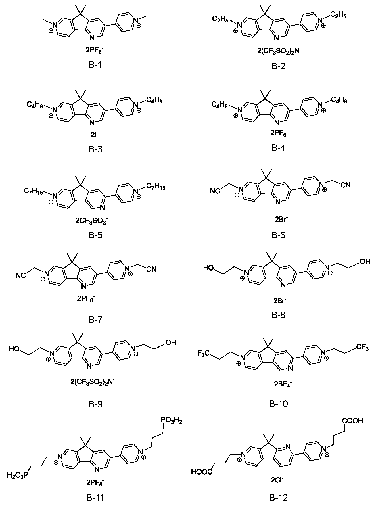
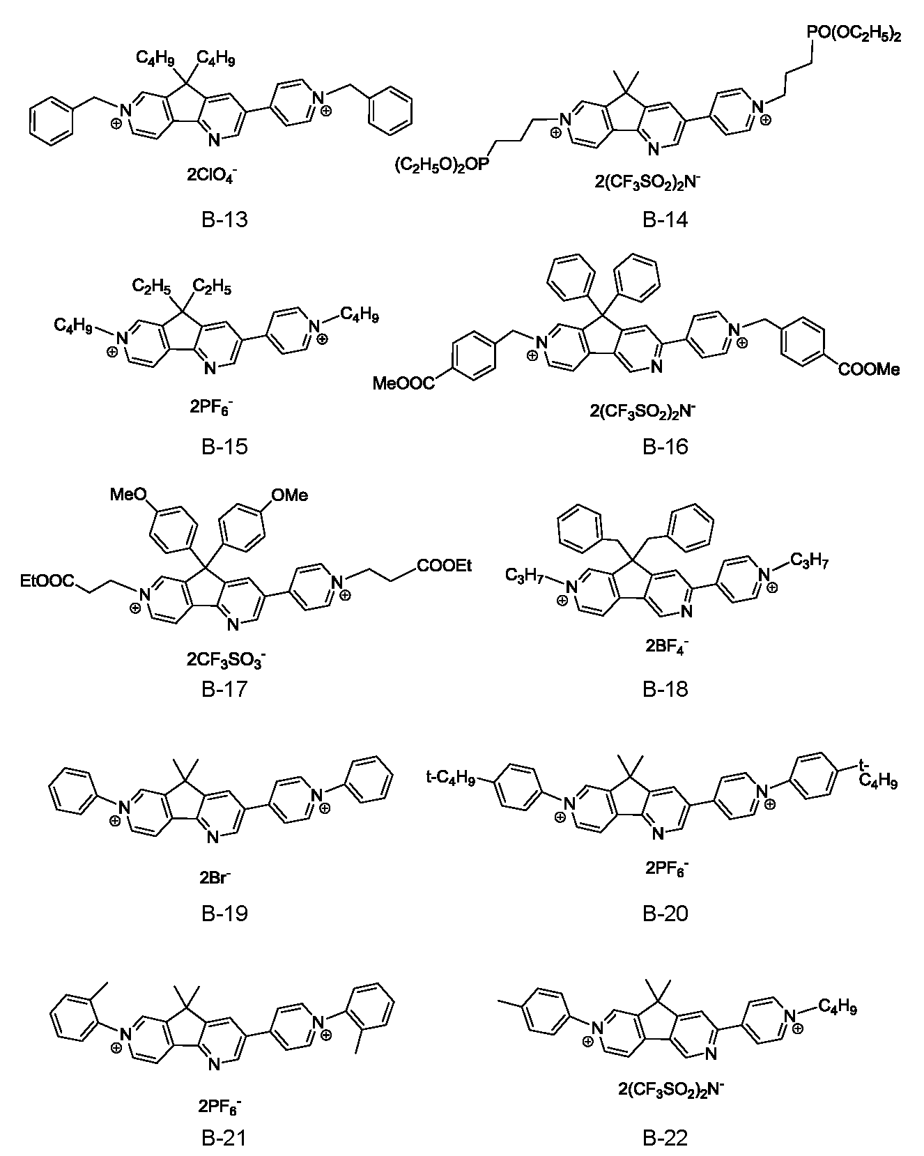
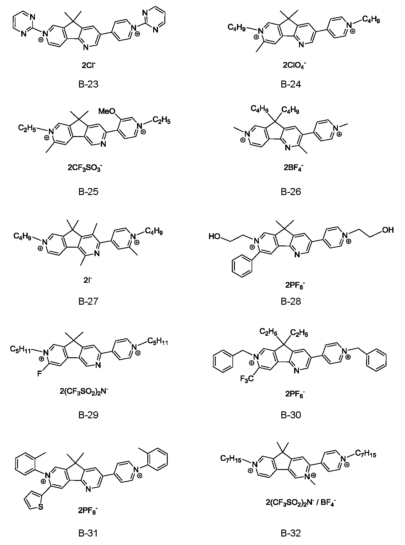
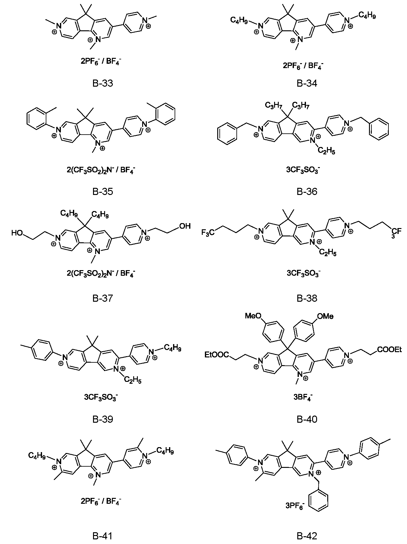
例示化合物のうちA群に示す化合物は、一般式[1]におけるY1乃至Y3が、いずれも炭素原子である化合物である。
例示化合物のうちB群に示す化合物は、一般式[1]におけるY1乃至Y3のうち、1つがN原子または(N+-L)(X-)で表され、残りの2つが炭素原子からなる構造である。
一方、C群に示す化合物は、一般式[1]におけるY1乃至Y3のうち、2つがN原子または(N+-L)(X-)で表され、残りの1つが炭素原子から構成される化学構造からなる化合物例である。
次に、本発明の一発明に係る有機化合物の構造に基づいた特性について説明する。一般式[1]で表される有機化合物は、還元状態で着色するカソード性のEC化合物である。すなわち、一般式[1]で表される有機化合物は、電気化学的な酸化還元反応が可逆的に進行することで、光学吸収の性質(呈色状態や光透過度)が変化する化合物である。
本発明の一実施形態に係る有機化合物は、一般式[1]の構造を有するため、着色時に450-540nmの波長の光を吸収することができる。
また、エレクトロクロミック素子に求められる特性の一つとして、低電圧駆動がある。低電圧駆動により消費電力が低減され、かつ長時間駆動や繰り返し耐久性が向上するからである。そして、低電圧駆動のためには、化合物のLUMO(最低空軌道)準位が低いことが好ましい。LUMO準位が低いとは、LUMO準位が深い、真空準位からより遠い、LUMOの絶対値が大きいということもできる。
本発明の一実施形態に係る一般式[1]で表されるカソード性EC化合物は、2つのピリジン環を連結する中央の芳香環がN原子を含んだヘテロ環から成る。そのため、電子密度が低くなり、LUMOが安定化(深く)なることにより電子が入れやすくなる、すなわち還元電位が正方向にシフトする。
この化学構造と還元電位の相関を比較するための例として、本発明の一実施形態に係る有機化合物(B-4、B-20、B-21)および(C-1、C-2、C-3)と、参考例化合物(Ref-1、Ref-2、Ref-3)について、分子軌道計算により検証した。

なお、化合物(B-4、B-20、B-21)は中央の芳香環のN原子が1個のピリジン環であり、化合物(C-1、C-2、C-3)は中央の芳香環のN原子が2個のピラジン環である。また、比較化合物(Ref-1、Ref-2、Ref-3)は中央の芳香環にN原子が含まれないベンゼン環であり、その他の化学構造は本発明の一実施形態に係る有機化合物(B-4、B-20、B-21)および(C-1、C-2、C-3)と同じである。分子軌道計算から求めた還元電位を下記表1から表3にまとめた。
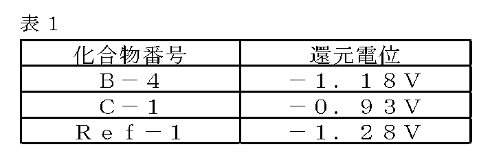
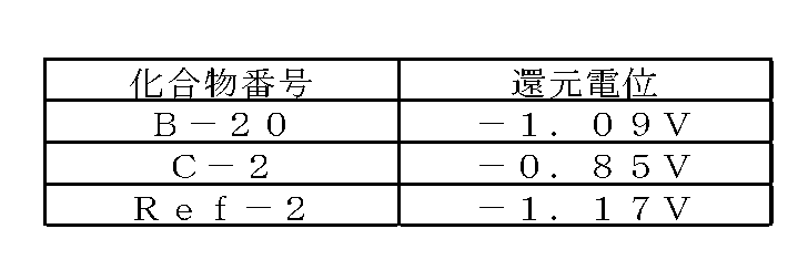

表1から表3に示すように、本発明の一実施形態に係る化合物(B-4、B-20、B-21)および(C-1、C-2、C-3)の還元電位は、いずれも参考例化合物(Ref-1、Ref-2、Ref-3)化合物の還元電位より正にシフトすることが確認された。参考化合物よりも、本発明に係る一実施形態に係る有機化合物の方が、EC素子の低電圧化に寄与することができる。
なお、分子軌道計算は、電子状態計算ソフトウェアであるGaussian03*Revision D.01を用いて基底状態の構造最適化計算を行ったものである。その際、量子化学計算法として、密度汎関数法(Density Functional Theory)を採用し、汎関数にはB3LYPを用いた。基底関数はGaussian 03, Revision D.01では6-31G*を用いた。
本計算を行うに当たり使用したプログラムは、 Gaussian 09, Revision D.01( M. J. Frisch, G. W. Trucks, H. B. Schlegel, G. E. Scuseria, M. A. Robb, J. R. Cheeseman, G. SCALMANI, V. Barone, B. Mennucci, G. A. Petersson, H. Nakatsuji, M. Caricato, X. Li, H. P. Hratchian, A. F. Izmaylov, J. Bloino, G. Zheng, J. L. Sonnenberg, M. Hada, M. Ehara, K. Toyota, R. Fukuda, J. Hasegawa, M. Ishida, T. Nakajima, Y. Honda, O. Kitao, H. Nakai, T. Vreven, J. A. Montgomery, Jr., J. E. Peralta, F. Ogliaro, M. Bearpark, J. J. Heyd, E. Brothers, K. N. Kudin, V. N. Staroverov, T. Keith, R. Kobayashi, J. Normand, K. Raghavachari, A. Rendell, J. C. Burant, S. S. Iyengar, J. Tomasi, M. Cossi, N. Rega, J. M. Millam, M. Klene, J. E. Knox, J. B. Cross, V. Bakken, C. Adamo, J. Jaramillo, R. Gomperts, R. E. Stratmann, O. Yazyev, A. J. Austin, R. Cammi, C. Pomelli, J. W. Ochterski, R. L. Martin, K. Morokuma, V. G. Zakrzewski, G. A. Voth, P. Salvador, J. J. Dannenberg, S. Dapprich, A. D. Daniels, O. Farkas, J. B. Foresman, J. V. Ortiz, J. Cioslowski, and D. J. Fox, Gaussian, Inc., Wallingford CT, 2013.)である。
本発明の一実施形態に係る有機化合物は、エレクトロクロミック素子のEC層として用いることができる。
以下、図面を参照しながら本実施形態に係るEC素子について説明する。
図1のEC素子は、一対の透明電極11と、この一対の電極の間に配置されている電解質と本発明に係るEC性有機化合物とを有するEC層12と、を有するEC素子である。一対の電極は、シール材13によって、電極間距離が一定となっている。このEC素子は、一対の電極が一対の透明基板10の間に配置されている。
EC層12は、本発明に係る有機化合物を有している。このEC層は、EC化合物からなる層と、電解質からなる層とを有していてもよい。また、EC化合物と電解質とを有する溶液としてEC層を設けてもよい。本実施形態に係るEC素子は、EC層が溶液層であるEC素子であることが好ましい。
次に、本実施形態に係るEC素子を構成する部材について説明する。
電解質としては、イオン解離性の塩であり、かつ溶媒に対して良好な溶解性、固体電解質においては高い相溶性を示すものであれば限定されない。中でも電子供与性を有する電解質が好ましい。これら電解質は、支持電解質と呼ぶこともできる。
電解質としては、例えば、各種のアルカリ金属塩、アルカリ土類金属塩などの無機イオン塩や4級アンモニウム塩や環状4級アンモニウム塩などがあげられる。
具体的にはLiClO4、LiSCN、LiBF4、LiAsF6、LiCF3SO3、LiPF6、LiI、NaI、NaSCN、NaClO4、NaBF4、NaAsF6、KSCN、KCl等のLi、Na、Kのアルカリ金属塩等や、(CH3)4NBF4、(C2H5)4NBF4、(n-C4H9)4NBF4、(n-C4H9)4NPF6、(C2H5)4NBr、(C2H5)4NClO4、(n-C4H9)4NClO4等の4級アンモニウム塩および環状4級アンモニウム塩等が挙げられる。
EC性有機化合物および電解質を溶かす溶媒としては、EC性有機化合物や電解質を溶解できるものであれば特に限定されないが、特に極性を有するものが好ましい。
具体的には水や、メタノール、エタノール、プロピレンカーボネート、エチレンカーボネート、ジメチルスルホキシド、ジメトキシエタン、γ-ブチロラクトン、γ-バレロラクトン、スルホラン、ジメチルホルムアミド、ジメトキシエタン、テトラヒドロフラン、アセトニトリル、プロピオンニトリル、3-メトキシプロピオンニトリル、ベンゾニトリル、ジメチルアセトアミド、メチルピロリジノン、ジオキソラン等の有機極性溶媒が挙げられる。これらは単独で用いてもよく、2種以上を併用してもよい。
さらに、上記EC媒体に、さらにポリマーやゲル化剤を含有させて粘稠性が高いもの若しくはゲル状としたもの等を用いることもできる。これらポリマーやゲル化剤は、増粘剤と呼ぶこともできる。増粘剤を有し、EC溶液の粘度を増すことで、有機化合物が会合体を形成しにくくなり、吸収スペクトルの温度依存性を低減することができる。したがって、EC溶液は、増粘剤を有することが好ましい。
EC溶液の粘度は、10から5000cPであってよく、50から1000cPであってよい。EC溶液の粘度は、150cP以下であってよく、好ましくは100cP以下、さらに好ましくは65cP以下である。また、EC溶液の粘度は、20cP以上であってよく、好ましくは50cP以上である。
増粘剤は、前記エレクトロクロミック層の重量を100wt%とした場合に、20wt%以下の重量比であってよい。好ましくは、1wt%以上15wt%以下であり、より好ましくは、5wt%以上10wt%以下である。
上記ポリマーとしては、特に限定されず、例えばポリアクリロニトリル、カルボキシメチルセルロース、ポリ塩化ビニル、ポリエチレンオキサイド、ポリプロピレンオキサイド、ポリウレタン、ポリアクリレート、ポリメタクリレート、ポリアミド、ポリアクリルアミド、ポリエステル、ナフィオン(登録商標)などが挙げられる。
次に、透明基板および透明電極について説明する。透明基板10としては、例えば、無色あるいは有色ガラス、強化ガラス等が用いられる他、無色あるいは有色の透明性樹脂が用いられる。なお、本実施形態において透明とは、可視光の透過率が70%以上の透過率であることを示す。
具体的には、ポリエチレンテレフタレート、ポリエチレンナフタレート、ポリノルボルネン、ポリアミド、ポリサルフォン、ポリエーテルサルフォン、ポリエーテルエーテルケトン、ポリフェニレンサルファイド、ポリカーボネート、ポリイミド、ポリメチルメタクリレート等が挙げられる。
電極材料11としては、例えば、酸化インジウムスズ合金(ITO)、フッ素ドープ酸化スズ(FTO)、酸化スズ(NESA)、酸化インジウム亜鉛(IZO)、酸化銀、酸化バナジウム、酸化モリブデン、金、銀、白金、銅、インジウム、クロムなどの金属や金属酸化物、多結晶シリコン、アモルファスシリコン等のシリコン系材料、カーボンブラック、グラファイト、グラッシーカーボン等の炭素材料などを挙げることができる。
また、ドーピング処理などで導電率を向上させた導電性ポリマー、例えば、ポリアニリン、ポリピロール、ポリチオフェン、ポリアセチレン、ポリパラフェニレン、ポリエチレンジオキシチオフェン(PEDOT)とポリスチレンスルホン酸の錯体なども好適に用いられる。
一対の電極間にEC層を保持するために、また、両電極間の距離を保つためにシール材13が好ましく用いられる。シール材13は、スペーサー材料を含有するなどして電極間の距離を保持する機能を有していてもよい。シール材13は一対の電極11の間に配置されており、本発明のEC性有機化合物を有する溶液12を収容するための空間を与えるものである。このシール材13としては、化学的に安定で、気体及び液体を透過しにくく、EC化合物の酸化還元反応を阻害しない材料であることが好ましい。具体的には、ガラスフリット等の無機材料、エポキシ系やアクリル系樹脂等の熱硬化または光硬化型材料、ポリイミド、ポリテトラフルオロエチレン、フッ素ゴム等を用いることができる。
本実施形態に係るEC素子は、一対の電極とスペーサーとによって、形成される液体注入口を有していてもよい。液体注入口からEC性有機化合物を有する組成物を封入したのちに、封止部材により注入口を覆い、さらに接着剤等で密閉することで素子とすることができる。封止部材は、接着剤とEC性有機化合物が接触しないように隔離する役割も担っている。
本実施形態に係るEC素子の形成方法は特に限定されず、一対の電極の間に設けた間隙に、真空注入法、大気注入法、メニスカス法等によって予め調製したEC性有機化合物を含有する液体12を注入する方法を用いることができる。一対の電極のそれぞれは、電極と基板とが一体となっている電極基板であってもよい。
本実施形態に係るEC素子1は、本発明に係る有機化合物と、この有機化合物とは別種の第2の有機化合物とを有してもよい。第2の有機化合物は、一種類でも複数種類でもよく、酸化状態で着色するアノード性EC化合物でも、還元状態で着色するカソード性EC化合物でも、その双方の性質を有する化合物であってもよい。本発明に係る有機化合物は還元状態において着色する化合物なので、第2の有機化合物は、酸化状態で着色するアノード性EC化合物であることが好ましい。
エレクトロクロミック層は、4種類以上のエレクトロクロミック化合物を有することで、吸収スペクトルを平坦に近づける構造であってよい。
酸化状態で着色するアノード性EC化合物とは、酸化状態における可視光の透過率が、還元状態における可視光の透過率よりも低い化合物である。可視光領域のいずれかの透過率が変化していればよく、可視光全域の透過率が変化していなくてもよい。
また第2の有機化合物に加えて、さらに第3の有機化合物を含んでいてもよい。本発明に係る有機化合物や、第2の有機化合物とは異なる波長域に着色吸収を有する第3の有機化合物を備えることにより、EC素子としての光吸収を幅広く制御することができる。この第3の有機化合物はアノード性EC化合物であってもカソード性EC化合物であってもよい。
他のEC化合物の消色時の吸収波長領域は、消色時は400nm以下が好ましい。消色時に高い透明性を有する素子を提供することができるためである。一方、着色時の吸収波長領域は400nm以上800nm以下の範囲が好ましく、より好ましくは400nm以上450nm以下、または600nm以上700nm以下である。
他のEC化合物を有することで、可視光領域の光を各波長で均一に吸収するEC素子とすることが好ましい。
本実施形態に係る他のEC化合物として、例えば、下記構造式の化合物があげられる。
酸化状態で着色する他のEC化合物としては、オリゴチオフェン類、5,10-ジヒドロ-5,10-ジメチルフェナジン、5,10-ジヒドロ-5,10-ジイソプロピルフェナジンなどのフェナジン系化合物、フェロセン、テトラ-t-ブチルフェロセン、チタノセンなどのメタロセン系化合物、N,N’,N,N’-テトラメチル-p-フェニレンジアミンなどのフェニレンジアミン系化合物、1-フェニル-2-ピラゾリンなどのピラゾリン系化合物などが挙げられる。
還元状態で着色する化合物としては、N,N’-ジヘプチルビピリジニウムジパークロレート、N,N’-ジヘプチルビピリジニウムジテトラフフオロボレート、N,N’-ジヘプチルビピリジニウムジヘキサフルオロホスフェート、N,N’-ジエチルビピリジニウムジパークロレート、N,N’-ジエチルビピリジニウムジテトラフルオロボレート、N,N’-ジエチルビピリジニウムジヘキサフルオロホスフェート、N,N’-ジベンジルビピリジニウムジパークロレート、N,N’-ジベンジルビピリジニウムジテトラフルオロボレート、N,N’-ジベンジルビピリジニウムジヘキサフルオロホスフェート、N,N’-ジフェニルビピリジニウムジパークロレート、N,N’-ジフェニルビピリジニウムジテトラフロロボレート、N,N’-ジフェニルビピリジニウムジヘキサフロロホスフェートなどのビオロゲン系化合物、2-エチルアントラキノン、2-t-ブチルアントラキノン、オクタメチルアントラキノンなどのアントラキノン系化合物、フェロセニウムテトラフルオロボレート、フェロセニウムヘキサフルオロホスフェートなどのフェロセニウム塩系化合物、スチリル化系化合物などが挙げられる。
本実施形態において、フェナジン系化合物とは、化学構造中に5,10-ジヒドロ-フェナジン骨格を含む化合物である。フェナジン系化合物は、5,10-ジヒドロフェナジンに置換基を有する化合物を含む。例えば、5,10-ジヒドロフェナジンの5、10位の水素原子が、メチル基、エチル基、プロピル基などのアルキル基、フェニル基等のアリール基に置換されてもよい。また、フェナジン系化合物は、5,10-ジヒドロフェナジンに炭素原子数1以上20以下のアルキル基を有する化合物であってよい。また、5,10-ジヒドロフェナジンに炭素原子数1以上20以下のアルコキシ基を有する化合物であってよい。また、5,10-ジヒドロフェナジンに炭素原子数4以上60以下のアリール基を有する化合物であってよい。他の化合物、例えばビオロゲン系化合物、についても同様である。
本実施形態に係るEC素子1が有するEC層12に含まれる化合物は、公知の方法により抽出し、分析することで、EC素子1に含まれていることを確認することができる。例えば、クロマトグラフィーにより抽出し、NMRで分析することが挙げられる。また、エレクトロクロミック層が固体である場合は、TOF-SIMSなどにより、分析することができる。
本実施形態に係るEC素子は消色時に高い透明性を有するとともに、着色時に高い光学濃度を与え、透過率を低くすることが可能であり、カメラ等の撮像素子への入射光量を大きく減光する際に好適に用いることができる。
本実施形態に係るEC素子1は、光学フィルタ、レンズユニット、撮像装置、窓材等に用いることができる。また、本実施形態に係るEC素子と、光反射面にEC素子を有する光反射部材と、を備えることで、エレクトロクロミックミラーとすることもできる。光反射部材は、電極や基板を兼ねてよい。
本発明の一実施形態に係る光学フィルタは、EC素子1とEC素子1に接続されている能動素子を有する。能動素子は、エレクトロクロミック素子を駆動し、エレクトロクロミック素子を通過する光の光量を調整する能動素子である。能動素子は、例えば、トランジスタやMIM素子が挙げられる。トランジスタは活性領域に、InGaZnOなどの酸化物半導体を有していてもよい。
光学フィルタは、本実施形態に係るEC素子1と、EC素子1に接続されている駆動装置とを有している。図2は、EC素子1の駆動装置20と、駆動装置20が駆動するEC素子1の一例を示す模式図である。本実施形態のEC素子1の駆動装置20は、駆動電源8、抵抗切替器9、および制御器7を有する。
駆動電源8は、EC層12に含まれるEC材料が電気化学反応を生じるのに必要な電圧をEC素子1に印加する。
制御器7によるEC素子の透過率の制御方法は、用いられる素子に適した方法が採用される。具体的には、所望の透過率の設定値に対して、予め規定されている条件をEC素子1に入力する方法や、透過率の設定値とEC素子1の透過率を比較して、設定値に合うように条件を選択して入力する方法が挙げられる。変化させるパラメータとしては、電圧、電流、デューティー比を挙げることができる。制御器7はEC素子1に対して、電圧制御方式であれば電圧を、電流制御方式であれば電流を、パルス幅変調方式であればデューティー比をそれぞれ増大または減少させることで、対応するEC素子の着色濃度を増大または減少し、結果として入射光を低減または増大することができる。
抵抗切替器9は、駆動電源8とEC素子1を含む閉回路中に、不示図の抵抗R1と抵抗R1よりも大きな抵抗R2とを切り替えて直列に接続するものである。抵抗R1の抵抗値としては、少なくとも素子閉回路の最も大きなインピーダンスよりも小さいことが好ましく、好ましくは10Ω以下である。抵抗R2の抵抗値としては、素子閉回路の最も大きなインピーダンスよりも大きいことが好ましく、好ましくは1MΩ以上である。なお、抵抗R2は空気であっても良い。この場合、厳密には閉回路は開回路となるが、空気を抵抗R2と見なすことで閉回路と考えることができる。制御器7は、抵抗切替器9に切替信号を送り、抵抗R1と抵抗R2のスイッチングを制御する。
本実施形態に係るレンズユニットは、複数のレンズと、EC素子1を有する光学フィルタとを有している。光学フィルタは、複数のレンズの間またはレンズの外側のいずれに設けられていてもよい。光学フィルタは、レンズの光軸上に設けられることが好ましい。
本実施形態の撮像装置は、光学フィルタと、この光学フィルタを通過した光を受光する受光素子と、を有する。
撮像装置とは、具体的には、カメラ、ビデオカメラ、カメラ付き携帯電話等が挙げられる。撮像装置は、受光素子を有する本体と、レンズを有するレンズユニットとが分離できる形態であってもよい。
ここで撮像装置が、本体と、レンズユニットとで分離できる場合は、撮像時に撮像装置とは別体の光学フィルタを用いる形態も本発明に含まれる。なお、係る場合、光学フィルタの配置位置としては、レンズユニットの外側、レンズユニットと受光素子との間、複数あるレンズの間(レンズユニットが複数のレンズを有する場合)等が挙げられる。
図3は、本実施形態の光学フィルタを用いた撮像装置100の構成の一例を説明する模式図である。
撮像装置100は、レンズユニット102と、撮像ユニット103と、を有する撮像装置である。
レンズユニット102は、光学フィルタ101と、複数のレンズ又はレンズ群を有する撮像光学系と、を有する。光学フィルタ101は、上述の本実施形態の光学フィルタである。
レンズユニット102は、例えば、図3Aにおいて、絞りより後でフォーカシングを行うリアフォーカス式のズームレンズを表している。物体側より順に正の屈折力の第1のレンズ群104、負の屈折力の第2のレンズ群105、正の屈折力の第3のレンズ群106、正の屈折力の第4のレンズ群107の4つのレンズ群を有する。第2のレンズ群105と第3のレンズ群106の間隔を変化させて変倍を行い、第4のレンズ群107の一部のレンズ群を移動させてフォーカスを行う。
レンズユニット102は、例えば、第2のレンズ群105と第3のレンズ群106との間に開口絞り108を有し、また、第3のレンズ群106と第4のレンズ群107との間に光学フィルタ101を有する。レンズユニットを通過する光は、各レンズ群104~107、絞り108および光学フィルタ101を通過するよう配置されており、開口絞り108および光学フィルタ101を用いた光量の調整を行うことができる。
レンズユニット102は、マウント部材(不図示)を介して撮像ユニット103に着脱可能に接続されている。
なお、本実施形態では、レンズユニット101内の第3のレンズ群106と第4のレンズ群107との間に光学フィルタ101が配置されているが、撮像装置100はこの構成に限定されない。例えば、光学フィルタ101は、開口絞り108の前(被写体側)あるいは後(撮像ユニット103側)のいずれにあってもよく、また、第1~第4のレンズ群104~107のいずれの前、後、レンズ群の間にあってもよい。なお、光学フィルタ101を光の収束する位置に配置すれば、光学フィルタ101の面積を小さくできるなどの利点がある。
また、レンズユニット102の構成も上述の構成に限定されず、適宜選択可能である。例えば、リアフォーカス式の他、絞りより前でフォーカシングを行うインナーフォーカス式であっても良く、その他方式であっても構わない。また、ズームレンズ以外にも魚眼レンズやマクロレンズなどの特殊レンズも適宜選択可能である。
撮像ユニット103は、ガラスブロック109と、受光素子110と、を有する。
ガラスブロック109は、ローパスフィルタやフェースプレートや色フィルタ等のガラスブロックである。
また、受光素子110は、レンズユニットを通過した光を受光するセンサ部であって、CCDやCMOS等の撮像素子が使用できる。また、フォトダイオードのような光センサであっても良く、光の強度あるいは波長の情報を取得し出力するものを適宜利用可能である。
図3Aのように、光学フィルタ101がレンズユニット102に組み込まれている場合、駆動装置はレンズユニット102内に配置されてもよく、レンズユニット102外に配置されてもよい。レンズユニット102外に配置される場合は、配線を通してレンズユニット102の内のEC素子1と駆動装置を接続し、駆動制御する。
また、上述の撮像装置100の構成では、光学フィルタ101がレンズユニット102の内部に配置されている。しかし、本発明はこの形態に限らず、光学フィルタ101は、撮像装置100内部の適当な箇所に配置され、受光素子110は光学フィルタ101を通過した光を受光するよう配置されていればよい。
図3Bは、光学フィルタが撮像装置に配置されている撮像装置の一例の模式図である。撮像ユニット103が光学フィルタ101を有している。図3Bにおいては、例えば光学フィルタ101は受光素子110の直前に配置されている。撮像装置自体が光学フィルタ101を内蔵する場合、接続されるレンズユニット102自体が光学フィルタ101を持たなくてもよいため、既存のレンズユニット102を用いた調光可能な撮像装置を構成することが可能となる。
本実施形態の撮像装置100は、光量調整と受光素子の組合せを有する製品に適用可能である。例えばカメラ、デジタルカメラ、ビデオカメラ、デジタルビデオカメラに使用可能であり、また、携帯電話やスマートフォン、PC、タブレットなど撮像装置を内蔵する製品にも適用できる。
また、本実施形態に係るEC素子1は、窓材に用いることもできる。図4Aは本実施形態に係るEC素子1を用いた窓を示す概観図であり、図4Bは図4AのX-X’断面図を示す模式である。
本発明の調光窓111は、EC素子1(光学フィルタ)と、それを挟持する透明板113と、全体を囲繞して一体化するフレーム112とから成る。光学フィルタは不示図の駆動装置を有しており、駆動装置はフレーム112内に一体化されていても良く、フレーム112外に配置され配線を通してEC素子1と接続されていても良い。
透明板113は光透過率が高い材料であれば特に限定されず、窓としての利用を考慮すればガラス素材であることが好ましい。
フレーム112は材質を問わないが、ポリカーボネート、アクリロニトリルブタジエンスチレン、ポリアルキレンフランジカルボキシレート、ポリ乳酸、ポリブタジエンテレフタレート等の樹脂、またはこれらの混合物を用いてよい。
フレームとは、光学フィルタの少なくとも一部を被覆し、一体化された形態を有するもの全般であってよい。
図4においてEC素子1は透明板113とは独立した構成部材であるが、例えば、EC素子1の透明基板10を透明板113と見なしても構わない。
係る調光窓は、例えば日中の太陽光の室内への入射量を調整する用途に適用できる。太陽の光量の他、熱量の調整にも適用できるため、室内の明るさや温度の制御に使用することが可能である。また、シャッターとして、室外から室内への眺望を遮断する用途にも適用可能である。このような調光窓は、建造物用のガラス窓の他に、自動車や電車、飛行機、船など乗り物の窓にも適用可能である。
また、本発明の一実施形態に係るエレクトロクロミック素子は、自動車等の移動体に設けられるエレクトロクロミックミラーに用いてもよい。エレクトロクロミックミラーは、エレクトロクロミック素子を投下した光を反射する光反射部材を有する。
このように、一般式[1]で表される有機化合物をEC層12に含むEC素子1を、光学フィルタ、レンズユニット、撮像装置、窓材等に用いることができる。本実施形態の光学フィルタ、レンズユニット、撮像装置、窓材のそれぞれは、一般式[1]で表される有機化合物単独、あるいは他の波長帯域の着色吸収を有するEC化合物と組み合わせることにより、様々な吸収色を提供することが可能となる。
また、本実施形態の撮像装置100によれば、光学フィルタ101を調光部材として用いることにより、調光量を一つのフィルタで適宜可変させることが可能となり、部材点数の削減や省スペース化といった利点がある。
以下、実施例により本発明をさらに具体的に説明していくが、本発明はこれらに限定されるものではない。
[実施例1]
<例示化合物A-19の合成>
<例示化合物A-19の合成>
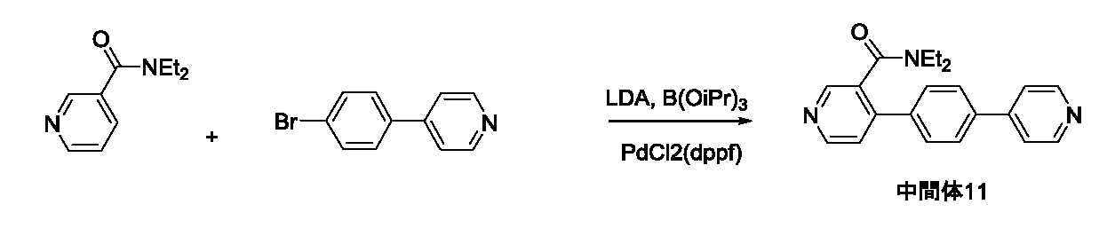
反応器にテトラヒドロフラン(8ml)、ジイソプロピルアミン(1.6ml、11mmol)を加え-70℃に冷却した。この溶液にゆっくりと1.6Mブチルリチウムヘキサン溶液(6.9ml、110mmol)滴下した後、0℃まで昇温し、LDA溶液を調整した。別途、N,N-ジエチルニコチンアミド(1.8g、10mmol)、ホウ酸トリイソプロピル(2.5ml、11mmol)、テトラヒドロフラン(8ml)を仕込み、-10℃まで冷却した。この溶液に、先に調整したLDA溶液をゆっくりと滴下し、室温で2時間撹拌を行った後、[1,1‘-ビス(ジフェニルホスフィノ)フェロセン]パラジウム(II)ジクロリドジクロロメタン付加物(0.17g、0.2mmol)、4-(4-ブロモフェニル)ピリジン(2.58g、11mmol)、テトラヒドロフラン(15ml)、リン酸カリウム(4.1g、25mmol)、水(15ml)を加え、60℃で14時間撹拌を行った。反応溶液を室温に放置した後、セライトろ過、酢酸エチルで抽出を行った。無水硫酸ナトリウムにて乾燥、濃縮し茶色固体を得た。これをカラム精製(溶離液:ヘキサン/酢酸エチル=1/2)し黄色の固体である中間体11(2.5g、収率74%)を得た。

反応器にテトラヒドロフラン(8ml)、ジイソプロピルアミン(1.3ml、9.1mmol)を加え-70℃に冷却した。この溶液にゆっくりと1.6Mブチルリチウムヘキサン溶液(5.7ml、9.1mmol)滴下した後、0℃まで昇温し、LDA溶液を調整した。この溶液に中間体11(2.5g、7.4mmol)のテトラヒドロフラン(10ml)溶液をゆっくりと滴下した後、室温に戻し、16時間撹拌を行った。飽和塩化アンモニウム溶液を加え、30分撹拌を行った後、ろ過により得られた結晶を水、メタノールで順次洗浄を行い灰色粉末の中間体12(1.3g、収率64%)を得た。
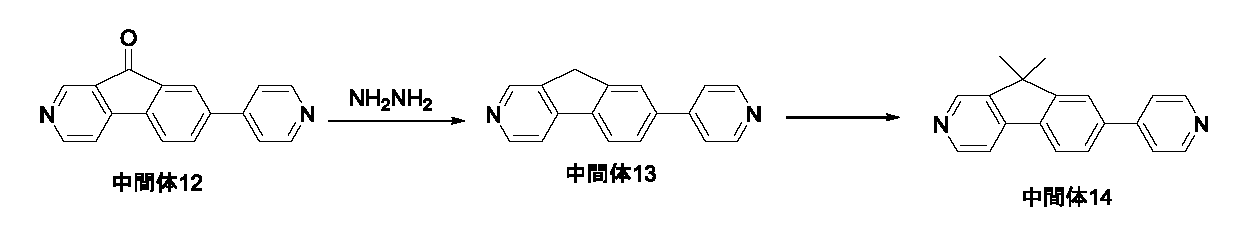
反応容器に中間体12(0.64g、2.5mmol)、ジエチレングリコール(6mL)、ヒドラジン一水和物(1.3ml,25mmol)を加え100℃で12時間加熱撹拌した。放冷後この溶液に水を加えた後、濃縮し固体を得た。これをカラム精製(溶離液:酢酸エチル/メタノール=10/1)し薄褐色の固体である中間体13(0.4g、収率65%)を得た。
反応容器に中間体13(0.4g、1.6mmol)、N,N-ジメチルホルムアミド(5mL)を加え氷浴で5℃に冷却した。この溶液にカリウムtert-ブトキシド(0.4g、3.4mmol)を加え同温で30分間撹拌後、N,N-ジメチルホルムアミド(5mL)に希釈したヨードメタン(0.2g、3.4mmol)を滴下した。同温で30分間撹拌後冷却バスを外し室温下で3時間撹拌した。反応液に飽和重曹水に加え、酢酸エチルにて抽出、有機層を合わせ、水、飽和食塩水で順次洗浄を行い、無水硫酸ナトリウムにて乾燥、濃縮し黒黄色固体を得た。これをカラム精製(溶離液:酢酸エチル/メタノール=10/1)しベージュ色の固体である中間体14(0.17g、収率39%)を得た。

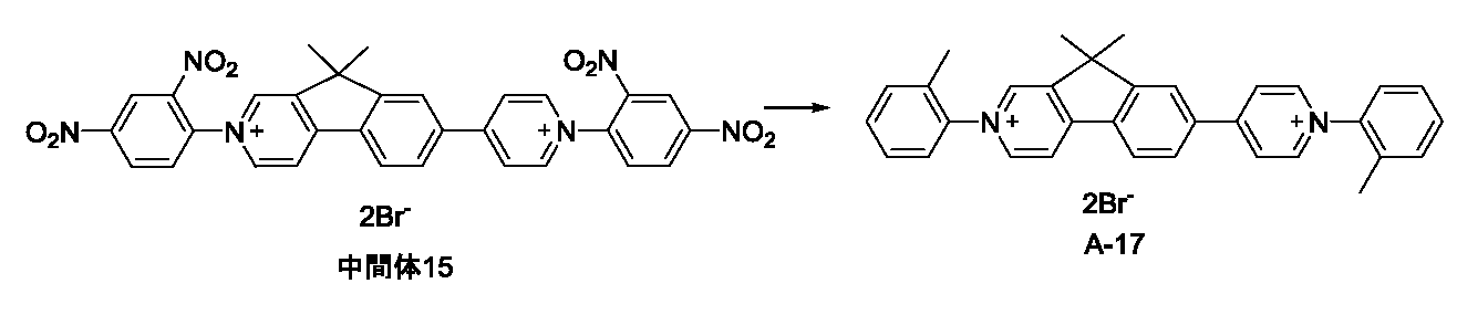
反応容器に中間体14(0.14g、0.5mmol)、2,4-ジニトロブロモベンゼン(0.36g、1.5mmol)、N‘,N’,-ジメチルホルムアミド10mlを反応容器に仕込み、100℃で24時間撹拌を行った。反応終了後、析出した結晶をろ過、アセトニトリルで洗浄し中間体15を0.29g(収率:75%)得た。

反応容器に中間体15(0.077g、0.1mmol)、4-t-ブチルアニリン(0.045g、0.3mmol)、エタノール10mlを反応容器に仕込み、加熱還流下8時間撹拌を行った。反応終了後、エタノールを真空除去した後、酢酸エチルを加え、沈殿を析出させた。沈殿をアセトニトリルで洗浄し例示化合物A-19を0.052g(収率:75%)得た。NMR測定によりこの化合物の構造を確認した。
1H NMR(CD3CN,500MHz) σ(ppm):9.12(s,1H),9.04(d,2H),8.92(d,1H),8.56(m,3H),8.45(d,1H),8.39(s,1H),8.23(m,1H),7.82(m,4H),7.73(m,4H),1.79(s,6H),1.44(s,9H),1.43(s,9H).
1H NMR(CD3CN,500MHz) σ(ppm):9.12(s,1H),9.04(d,2H),8.92(d,1H),8.56(m,3H),8.45(d,1H),8.39(s,1H),8.23(m,1H),7.82(m,4H),7.73(m,4H),1.79(s,6H),1.44(s,9H),1.43(s,9H).
[実施例2]
<例示化合物A-20の合成>
例示化合物A-19(0.035g、0.05mmol)を水に溶解させ、ビス(トリフルオロメタンスルホニル)イミドリチウム(0.29g、1mmol)を溶解した水溶液を滴下し、室温で3時間撹拌した後、ろ過し、得られた結晶を、エタノールで再結晶を行い、例示化合物A-20を0.051g(収率:92%)得た。NMR測定によりこの化合物の構造を確認した。
1H NMR(CD3CN,500MHz) σ(ppm):9.12(s,1H),9.04(d,2H),8.92(d,1H),8.56(m,3H),8.45(d,1H),8.39(s,1H),8.23(m,1H),7.82(m,4H),7.73(m,4H),1.79(s,6H),1.44(s,9H),1.43(s,9H).
[実施例3]
<例示化合物A-17の合成>
<例示化合物A-17の合成>
反応容器に中間体15(0.077g、0.1mmol)、o-トルイジン(0.064g、0.6mmol)、エタノール10mlを反応容器に仕込み、加熱還流下8時間撹拌を行った。反応終了後、エタノールを真空除去した後、酢酸エチルを加え、沈殿を析出させた。沈殿をアセトニトリルで洗浄し例示化合物A-17を0.042g(収率:68%)得た。NMR測定によりこの化合物の構造を確認した。
1H NMR(DMSO-d6,500MHz) σ(ppm):9.65(s,1H),9.40(d,2H),9.28(d,1H),8.96(d,1H),8.90(d,2H),8.77(s,1H),8.70(d,1H),8.51(d,1H),7.75-7.55(m,8H),2.23(s,6H),1.77(s,6H).
1H NMR(DMSO-d6,500MHz) σ(ppm):9.65(s,1H),9.40(d,2H),9.28(d,1H),8.96(d,1H),8.90(d,2H),8.77(s,1H),8.70(d,1H),8.51(d,1H),7.75-7.55(m,8H),2.23(s,6H),1.77(s,6H).
[実施例4]
<例示化合物A-18の合成>
例示化合物A-17(0.031g、0.05mmol)を水に溶解させ、ビス(トリフルオロメタンスルホニル)イミドリチウム(0.29g、1mmol)を溶解した水溶液を滴下し、室温で3時間撹拌した後、ろ過し、得られた結晶を、エタノールで再結晶を行い、例示化合物A-18を0.047g(収率:92%)得た。NMR測定によりこの化合物の構造を確認した。
1H NMR(CD3CN,500MHz) σ(ppm):8.97(s,1H),8.88(d,2H),8.76(d,1H),8.59(m,3H),8.48(d,1H),8.38(s,1H),8.23(m,1H),7.75-7.55(m,8H),2.24(s,6H),1.77(s,6H).
[実施例5]
<例示化合物B-3の合成>
<例示化合物B-3の合成>
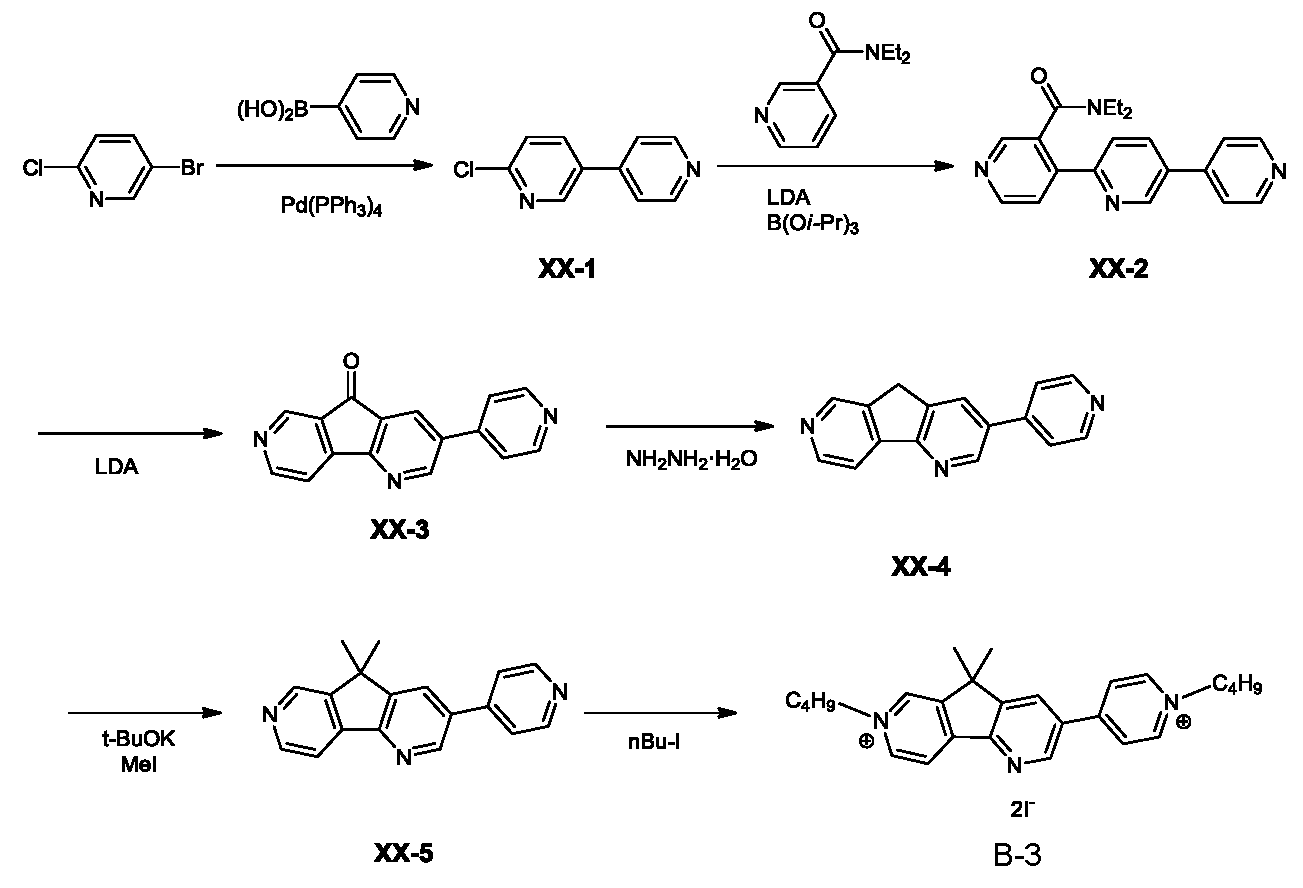
(1)XX-1の合成:1Lの反応容器で、5-ブロモ-2-クロロピリジン:19.24g(100mmol),4-ピリジルボロン酸:14.75g(120mmol)を、1,4-ジオキサン/純水(500ml/100ml)中混合し、窒素で溶存酸素を除去した。
次にPd(PPh3)4:1.16g(1.0mmol)および、リン酸カリウム:31.84g(150mmol)を窒素雰囲気下添加し、90℃にて17時間反応を行った。
反応溶液を室温に冷却後、水層を酢酸エチルで抽出し、シリカゲルクロマトグラフィー(移動相:ヘキサン/酢酸エチル)により分離精製し、XX-1を得た(7.99g、収率41.9%)。
(2)XX-2の合成:50ml反応器にテトラヒドロフラン(25ml)、ジイソプロピルアミン(4.7ml、33mmol)を加え-70℃に冷却した。この溶液にゆっくりと1.6Mブチルリチウムヘキサン溶液(21ml、33mmol)を滴下した後、0℃まで昇温し、LDA溶液を調製した。別途、N,N-ジエチルニコチンアミド(5.35g、30mmol)、ホウ酸トリイソプロピル(7.6ml、33mmol)、テトラヒドロフラン(25ml)を仕込み、-50℃まで冷却した。この溶液に、先に調製したLDA溶液をゆっくりと滴下し、0℃で2時間撹拌を行った後、減圧濃縮した。これに、XX-1(4.72g、30mmol)、リン酸カリウム(10.73g、75mmol)、窒素バブリングした1,4-ジオキサン/純水(150ml/45ml)を加え混合した。さらに、トリス(ジベンジリデンアセトン)ジパラジウム(550mg、0.6mmol)、0.6Mトリシクロヘキシルホスフィントルエン溶液(2.2ml、1.32mmol)を加え、90℃で21時間撹拌を行った。反応溶液を室温に放冷した後、酢酸エチルで抽出を行い、カラム精製(移動相:ヘキサン/酢酸エチル)により、薄緑色固体であるXX-2(4.29g、収率43%)を得た。
(3)XX-3の合成:反応器にテトラヒドロフラン(15ml)、ジイソプロピルアミン(2ml、14mmol)を加え、-70℃に冷却した。この溶液にゆっくりと1.6Mブチルリチウムヘキサン溶液(9ml、13mmol)滴下した後、0℃まで昇温し、LDA溶液を調製した。この溶液を-50℃に冷却し、XX-2(4.29g、12.9mmol)のテトラヒドロフラン(50ml)溶液をゆっくりと滴下した後、室温に戻し、4時間撹拌を行った。飽和塩化アンモニウム溶液を加えた後、ろ過により得られた結晶を水、メタノールで順次洗浄を行い薄緑色粉末のXX-3(2.7g、収率81%)を得た。
(4)XX-4の合成:反応容器にXX-3(2.73g、10.5mmol)、ジエチレングリコール(24mL)、ヒドラジン一水和物(5.2ml、105mmol)を加え150℃で12時間加熱撹拌した。放冷後この溶液に水を加え、析出した固体をろ過、アセトニトリルで洗浄することで、薄褐色の固体であるXX-4(1.80g、収率70%)を得た。
(5)XX-5の合成:反応容器にXX-4(736mg、3mmol)、N,N-ジメチルホルムアミド(10mL)を加え氷浴で5℃に冷却した。この溶液にカリウムtert-ブトキシド(707mg、6.3mmol)、ヨードメタン(0.39ml、6.3mmol)を滴下した。同温で30分間撹拌後、冷却バスを外し室温で3時間撹拌した。反応液に飽和重曹水を加え、酢酸エチルにて抽出し、カラム精製(移動相:ヘキサン/酢酸エチル)により、淡褐色固体のXX-5(345mg、収率42%)を得た。
(6)B-3の合成:反応容器にXX-5(147mg、0.54mmol)と1-ヨードブタン:594mg(3.2mmol)、アセトニトリル5mlとを加え、90℃にて加熱還流し20時間反応を行った。反応終了後、析出した結晶を濾過しアセトンで洗浄して例示化合物B-3を得た(265mg、収率76%)。
核磁気共鳴スペクトル(NMR)測定の測定により、得られた化合物の構造確認を行った。その結果、ピーク積分値の比がその構造と良く一致し、得られた化合物は例示化合物B-3であることを確認した。NMRスペクトルの測定結果を以下に示す。
1H NMR(DMSO-d6) δ(ppm):9.47(s,1H),9.49(d,1H),9.28(d,2H),9.17(d,1H),9.05(d,1H),8.77(d,2H),8.66(d,1H),4.66(t,4H),1.95(m,4H),1.73(s,6H),1.35(m,4H),0.93(t,6H).
1H NMR(DMSO-d6) δ(ppm):9.47(s,1H),9.49(d,1H),9.28(d,2H),9.17(d,1H),9.05(d,1H),8.77(d,2H),8.66(d,1H),4.66(t,4H),1.95(m,4H),1.73(s,6H),1.35(m,4H),0.93(t,6H).
[実施例6]
<例示化合物B-4の合成>

<例示化合物B-4の合成>
例示化合物B-3(261mg、0.41mmol)を水に溶解した。ヘキサフルオロリン酸アンモニウム320mgを溶解した水溶液を滴下し、室温で3時間撹拌を行った。析出した結晶をろ過、水、イソプロピルアルコール、ジエチルエーテルで順次で洗浄し、例示化合物B-4を235mg(収率:85%)得た。
NMR測定によりこの化合物の構造を確認した。
1H NMR(CD3CN) δ(ppm):9.27(d,1H),8.99(s,1H),8.82(d,2H),8.76(d,1H),8.61(d,1H),8.51(d,1H),8.43(d,2H),4.58(t,4H),2.06(m,4H),1.73(s,6H),1.43(m,4H),1.01(t,6H).
1H NMR(CD3CN) δ(ppm):9.27(d,1H),8.99(s,1H),8.82(d,2H),8.76(d,1H),8.61(d,1H),8.51(d,1H),8.43(d,2H),4.58(t,4H),2.06(m,4H),1.73(s,6H),1.43(m,4H),1.01(t,6H).
[実施例7]
<例示化合物B-34の合成>

<例示化合物B-34の合成>
反応容器に例示化合物B-4(205mg、0.30mmol)とジクロロメタン(6ml)を加え、さらにトリメチルオキソニウムテトラフルオロボレート(444mg、3.0mmol)を加えた後、室温で2日間撹拌した。析出した固体をろ過し、ジクロロメタン、メタノール、ジエチルエーテルで順次で洗浄し、例示化合物B-34を75mg(収率:30%)得た。
NMR測定によりこの化合物の構造を確認した。
1H NMR(CD3CN) δ(ppm):9.35(s,1H),9.26(s,2H),9.01-8.95(m,3H),8.76(d,1H),8.52(d,2H),4.84(s,3H),4.71(t,2H),4.66(t,2H),2.01(m,4H),1.82(s,6H),1.48(m,4H),1.04(t,6H).
1H NMR(CD3CN) δ(ppm):9.35(s,1H),9.26(s,2H),9.01-8.95(m,3H),8.76(d,1H),8.52(d,2H),4.84(s,3H),4.71(t,2H),4.66(t,2H),2.01(m,4H),1.82(s,6H),1.48(m,4H),1.04(t,6H).
[実施例8]
<例示化合物B-6の合成>

反応容器に、実施例5で合成したXX-5(104mg、0.38mmol)とブロモアセトニトリル(228mg、1.90mmol)、アセトニトリル4mlとを加え、90℃にて加熱還流し20時間反応を行った。反応終了後、析出した結晶を濾過し酢酸エチルで洗浄して例示化合物B-6を得た(140mg、収率72%)。
<例示化合物B-6の合成>
反応容器に、実施例5で合成したXX-5(104mg、0.38mmol)とブロモアセトニトリル(228mg、1.90mmol)、アセトニトリル4mlとを加え、90℃にて加熱還流し20時間反応を行った。反応終了後、析出した結晶を濾過し酢酸エチルで洗浄して例示化合物B-6を得た(140mg、収率72%)。
NMR測定によりこの化合物の構造を確認した。
1H NMR(DMSO-d6) δ(ppm):9.77(s,1H),9.54(d,1H),9.39(d,2H),9.26(d,1H),9.13(d,1H),8.88(d,2H),8.76(d,1H),6.08(s,2H),6.01(s,2H),1.73(s,6H).
1H NMR(DMSO-d6) δ(ppm):9.77(s,1H),9.54(d,1H),9.39(d,2H),9.26(d,1H),9.13(d,1H),8.88(d,2H),8.76(d,1H),6.08(s,2H),6.01(s,2H),1.73(s,6H).
[実施例9]
<例示化合物B-7の合成>

<例示化合物B-7の合成>
反応容器で例示化合物B-6(140mg、0.27mmol)を水10mlに溶解した。ヘキサフルオロリン酸アンモニウム160mgを溶解した水溶液を滴下し、室温で3時間撹拌を行った。析出した結晶をろ過、水、イソプロピルアルコール、ジエチルエーテルで順次で洗浄し、例示化合物B-7を120mg(収率:69%)得た。NMR測定によりこの化合物の構造を確認した。
1H NMR(CD3CN) δ(ppm):9.30(d,1H),9.08(s,1H),8.92(d,2H),8.87(d,1H),8.65(d,1H),8.59(d,1H),8.52(d,2H),5.65(s,2H),5.64(s,2H),1.73(s,6H).
1H NMR(CD3CN) δ(ppm):9.30(d,1H),9.08(s,1H),8.92(d,2H),8.87(d,1H),8.65(d,1H),8.59(d,1H),8.52(d,2H),5.65(s,2H),5.64(s,2H),1.73(s,6H).
[実施例10]
<例示化合物B-20の合成>

<例示化合物B-20の合成>
反応容器に、実施例1で合成したXX-5(150mg、0.55mmol)とビス(4-tert-ブチルフェニル)ヨードニウムヘキサフルオロホスフェート(1.13g、2.47mmol)、酢酸銅(II)一水和物(10.0mg、0.055mmol)、N,N-ジメチルホルムアミド(2.5mL)とを加え、100℃にて24時間反応を行った。反応終了後、減圧濃縮し、テトラブチルアンモニウムブロミド(1g)のアセトニトリル溶液(5ml)を加えた。析出した固体を濾過回収し、水10mlに溶解した。これにヘキサフルオロリン酸アンモニウム220mgを溶解した水溶液を滴下し、室温で3時間撹拌を行った。析出した結晶をろ過、水、イソプロピルアルコール、ジエチルエーテルで順次で洗浄し、例示化合物B-20を290mg(収率:64%)得た。
NMR測定によりこの化合物の構造を確認した。
1H NMR(CD3CN) δ(ppm):9.39(d,1H),9.23(s,1H),9.07(d,2H),8.99(d,1H),8.72(d,1H),8.65(d,1H),8.60(d,2H),7.83-7.70(m,8H),1.80(s,6H),1.43(s,9H),1.42(s,9H).
1H NMR(CD3CN) δ(ppm):9.39(d,1H),9.23(s,1H),9.07(d,2H),8.99(d,1H),8.72(d,1H),8.65(d,1H),8.60(d,2H),7.83-7.70(m,8H),1.80(s,6H),1.43(s,9H),1.42(s,9H).
[実施例11]
<エレクトロクロミック素子の作製及び特性評価>
電解質として過塩素酸テトラブチルアンモニウムを0.1Mの濃度で炭酸プロピレンに溶解させ、次いで実施例2の例示化合物A-20を40.0mMの濃度で溶解させ、EC媒体を得た。
<エレクトロクロミック素子の作製及び特性評価>
電解質として過塩素酸テトラブチルアンモニウムを0.1Mの濃度で炭酸プロピレンに溶解させ、次いで実施例2の例示化合物A-20を40.0mMの濃度で溶解させ、EC媒体を得た。
次いで一対の透明導電膜(ITO)付きのガラス基板の四方の端部に絶縁層(SiO2)を形成した。基板間隔を規定するPETフィルム(帝人デュポンフィルム社製メリネックスS(登録商標)、125μm厚)を一対の透明電極膜付きガラス基板の間に配置した。その後、EC媒体注入用の注入口を残してエポキシ系接着剤により基板と、PETフィルムを接着し、封止した。以上のように、注入口付き空セルを作製した。
次に前述の注入口より、上で得られたEC媒体を真空注入法により注入後、注入口をエポキシ系接着剤により封止し、EC素子とした。
作製直後の本EC素子は可視光領域全域にわたり、80%前後の透過率を示し、高い透明性を有していた。
この素子に電圧を2.0V印加すると、例示化合物A-20の還元種に由来する吸収(λmax=536nm)を示し、素子は着色した。さらに-0.5V印加すると消色した。この素子は着色状態と、消色状態と、を可逆的に変化できる。図5は、実施例10で作製した素子の紫外可視吸収スペクトルである。光源には、オーシャンオプティクス社のDH‐2000S重水素、ハロゲン光源を用いた。
[実施例12]
<エレクトロクロミック素子の作製及び特性評価>
実施例11において、例示化合物A-20の代わりに例示化合物A-18を使用した以外は、実施例11と同様の方法により素子を作製した。本実施例の素子に電圧を2.0V印加すると、例示化合物A-18の還元種に由来する吸収(λmax=520nm)を示し、素子は着色した。さらに-0.5V印加すると消色し、可逆的な着色及び消色した。この素子は着色状態と、消色状態と、を可逆的に変化できる。図6は、実施例12で作製した素子の紫外可視吸収スペクトルである。
<エレクトロクロミック素子の作製及び特性評価>
実施例11において、例示化合物A-20の代わりに例示化合物A-18を使用した以外は、実施例11と同様の方法により素子を作製した。本実施例の素子に電圧を2.0V印加すると、例示化合物A-18の還元種に由来する吸収(λmax=520nm)を示し、素子は着色した。さらに-0.5V印加すると消色し、可逆的な着色及び消色した。この素子は着色状態と、消色状態と、を可逆的に変化できる。図6は、実施例12で作製した素子の紫外可視吸収スペクトルである。
[実施例13および比較例1]
<エレクトロクロミック特性の評価>
例示化合物B-20について、酸化還元電位の測定、および透過率スペクトル測定を行った。
<エレクトロクロミック特性の評価>
例示化合物B-20について、酸化還元電位の測定、および透過率スペクトル測定を行った。
測定は、支持電解質としてのテトラブチルアンモニウムヘキサフルオロホスファートの炭酸プロピレン溶液(0.1mol/L)中に例示化合物B-20を溶解(2.0×10-3mol/L)した溶液を用いて行った。この溶液を、光路長1mmのガラスセル中に入れ、メッシュ状の白金電極(作用電極)とワイヤー状の白金電極(対向電極)を並べ、参照電極RE(Ag/Ag+)を配置して測定を行った。
酸化還元電位は、サイクリックボルタンメトリー(CV)により測定した。なお、還元電位の評価はフェロセンを基準物質として測定した。
透過率スペクトル測定は、溶液に対して、化合物の還元電位以上で定電位還元を行うことにより、メッシュ電極を通過する透過光を用いて行った。電圧の印加にはソーラートロン社製ポテンシオスタット(セルテスト1470E)を、分光測定にはオーシャンオプティクス社製分光器(USB2000-UV-VIS)を使用した。
CV測定の結果、例示化合物B-20の還元電位は-0.99Vであった。結果を表4にまとめた。
図7は、例示化合物B-20の消色状態および着色状態(還元状態)の透過率スペクトルである。例示化合物B-20は消色状態では可視光領域全体にわたって吸収を持たず、透明性が高い材料である。一方、還元着色時には可視域で透過率が変化し、その吸収ピークの波長λmaxは528nmであった。この還元着色状態は、酸化により再度無色透明に戻り、酸化還元に伴う可逆的なエレクトロクロミック特性が確認された。
一方比較例として、カソード性EC化合物Ref-2を使用した測定結果について述べる。
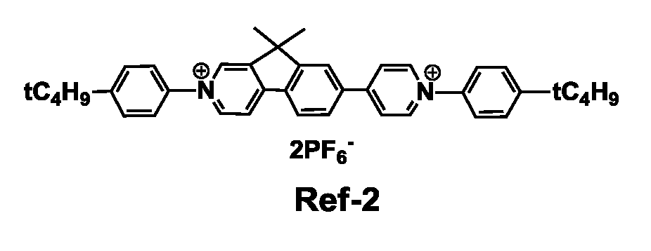
参考例のカソード性EC化合物Ref-2は、例示化合物B-20の中央のピリジン環がベンゼン環である以外は同じ化学構造の化合物である。Ref-2は、還元状態において、カソード性EC化合物B-20とほぼ同じ着色吸収波長を示す(λmax~536nm)が、還元電位は-1.14Vであり、例示化合物B-20より150mV負の還元電位を示した。結果を表4にまとめた。
[実施例14]
<エレクトロクロミック特性の評価>
例示化合物B-20の代わりに例示化合物B-7を用いた以外は、実施例13と同様の方法で測定を行った。結果を表4にまとめた。
<エレクトロクロミック特性の評価>
例示化合物B-20の代わりに例示化合物B-7を用いた以外は、実施例13と同様の方法で測定を行った。結果を表4にまとめた。
[実施例15]
<エレクトロクロミック特性の評価>
例示化合物B-20の代わりに例示化合物B-34を用いた以外は、実施例13と同様の方法で測定を行った。結果を表4にまとめた。
<エレクトロクロミック特性の評価>
例示化合物B-20の代わりに例示化合物B-34を用いた以外は、実施例13と同様の方法で測定を行った。結果を表4にまとめた。
[実施例16]
<エレクトロクロミック特性の評価>
例示化合物B-20の代わりに例示化合物B-4を用いた以外は、実施例13と同様の方法で測定を行った。結果を表4にまとめた。
<エレクトロクロミック特性の評価>
例示化合物B-20の代わりに例示化合物B-4を用いた以外は、実施例13と同様の方法で測定を行った。結果を表4にまとめた。
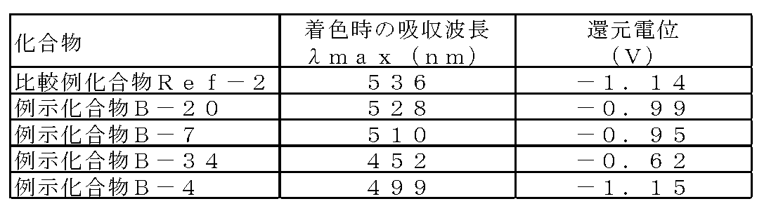
[実施例17]
<エレクトロクロミック素子の作製および特性評価>
カソード性EC材料として例示化合物B-20、アノード性EC材料として下記構造のW-1(5、10-ジイソプロピル-5、10-ジヒドロフェナジン)をそれぞれ100mMの濃度で炭酸プロピレンに溶解させ、さらに増粘剤としてポリメチルメタクリレート(PMMA)を5wt%添加し、EC溶液を調製した。
<エレクトロクロミック素子の作製および特性評価>
カソード性EC材料として例示化合物B-20、アノード性EC材料として下記構造のW-1(5、10-ジイソプロピル-5、10-ジヒドロフェナジン)をそれぞれ100mMの濃度で炭酸プロピレンに溶解させ、さらに増粘剤としてポリメチルメタクリレート(PMMA)を5wt%添加し、EC溶液を調製した。

次いで、インジウムドープ酸化スズ(ITO)膜が成膜されている透明導電性ガラスを2枚用意し、ITO膜同士が対向するように配置した。そして、2枚の透明導電性ガラスの外周を、粒径50μmのスペーサービーズを混合したエポキシ系シール材を用いて接着した。アノード性EC化合物と、カソード性EC化合物とを溶解させた溶液を透明導電性ガラスに予め形成した注入口から注入することで、2枚の透明導電性ガラスとシール材によって形成されている空間内に当該溶液を充填した。その後、UV硬化型シール剤で注入口を封止して、EC素子を得た。
このEC素子に、駆動電圧0.9Vを印加すると、例示化合物B-20の還元種に由来する吸収(λ~528nm)およびアノード性EC化合物W-1の酸化種に由来する吸収(λ~480nm)を示し、EC素子は着色した。EC素子は0Vを印加すると消色し、可逆的な着消色を示した。
本発明の一実施形態に係る有機化合物は、着色時に450-540nmの波長の光を吸収するカソード性のエレクトロクロミック化合物である。この領域の光を吸収するEC素子、それを用いた光学フィルタ、レンズユニットおよび撮像装置等に利用することができる。
本発明は上記実施の形態に制限されるものではなく、本発明の精神及び範囲から離脱することなく、様々な変更及び変形が可能である。従って、本発明の範囲を公にするために以下の請求項を添付する。
本願は、2018年6月28日提出の日本国特許出願特願2018-123695と2019年3月15日提出の日本国特許出願特願2019-048986と2019年4月25日提出の日本国特許出願特願2019-084741を基礎として優先権を主張するものであり、その記載内容の全てをここに援用する。
Claims (22)
- 下記一般式[1]で表されることを特徴とする有機化合物。

一般式[1]において、Z1およびZ2は置換基を有してもよいアルキル基、置換基を有してもよいアリール基および置換基を有してもよいアラルキル基からそれぞれ独立に選ばれる。
R11乃至R17は、水素原子または置換基からそれぞれ独立に選ばれる。前記置換基は、置換基を有してもよいアルキル基、置換基を有してもよいアルコキシ基、置換基を有してもよいアリール基、または置換基を有してもよい複素環基またはハロゲン原子のいずれかである。R16とR17は、互いに結合して環を形成してもよい。
R21およびR22は、水素原子または置換基からそれぞれ独立に選ばれる。前記置換基は、置換基を有してもよいアルキル基、置換基を有してもよいアリール基または置換基を有してもよいアラルキル基のいずれかである。
Y1乃至Y3は、炭素原子、N原子、または(N+-L)(X-)からそれぞれ独立に選ばれる。Lは置換基を有してもよいアルキル基、置換基を有してもよいアリール基、置換基を有してもよいアラルキル基のいずれかである。 - 前記Y1乃至Y3がいずれも、炭素原子であることを特徴とする請求項1に記載の有機化合物。
- 前記Y1およびY2がそれぞれ独立に、N原子または(N+-L)(X-)であり、Y3が炭素原子であることを特徴とする請求項1に記載の有機化合物。
- 前記Y1乃至Y3のいずれか1つがN原子または(N+-L)(X-)であり、他の2つが炭素原子であることを特徴とする請求項1に記載の有機化合物。
- 前記Y1がN原子または(N+-L)(X-)であり、他の2つが炭素原子であることを特徴とする請求項1に記載の有機化合物。
- Z1およびZ2が、前記アリール基であることを特徴とする請求項1乃至5のいずれか一項に記載の有機化合物。
- Z1およびZ2が、前記アリール基のうちのフェニル基であり、前記フェニル基は、アルキル基を置換基として有することを特徴とする請求項6に記載の有機化合物。
- 前記アルキル基は、前記一般式[1]の基本骨格に対して、パラ位に置換していることを特徴とする請求項7に記載の有機化合物。
- 前記アルキル基は、前記一般式[1]の基本骨格に対して、オルト位に置換していることを特徴とする請求項7に記載の有機化合物。
- 前記アルキル基は、炭素原子数1乃至8のアルキル基であることを特徴とする請求項8または9に記載の有機化合物。
- 一対の電極と、前記一対の電極の間に配置されているエレクトロクロミック層を有するエレクトロクロミック素子であって、
前記エレクトロクロミック層は、請求項1乃至10のいずれか一項に記載の有機化合物を含有することを特徴とするエレクトロクロミック素子。 - 前記エレクトロクロミック層は前記有機化合物とは別種の第2のエレクトロクロミック化合物をさらに有する請求項11に記載のエレクトロクロミック素子。
- 前記第2のエレクトロクロミック化合物は、酸化状態における可視光の透過率が還元状態における可視光の透過率よりも低い、アノード性EC化合物である請求項12に記載のエレクトロクロミック素子。
- 前記エレクトロクロミック層は、4種類以上のエレクトロクロミック化合物を有することを特徴とする請求項11乃至13のいずれか一項に記載のエレクトロクロミック素子。
- 前記4種類以上のエレクトロクロミック化合物には、ビオロゲン系化合物、フェナジン系化合物が含まれることを特徴とする請求項14に記載のエレクトロクロミック素子。
- 前記エレクトロクロミック層は、溶液層であることを特徴とする請求項11乃至15のいずれか一項に記載のエレクトロクロミック素子。
- 前記エレクトロクロミック層は、増粘剤をさらに有することを特徴とする請求項16に記載のエレクトロクロミック素子。
- 前記増粘剤の重量比が、前記エレクトロクロミック層の重量を100wt%とした場合に、20wt%以下であることを特徴とする請求項17に記載のエレクトロクロミック素子。
- 請求項11乃至18のいずれか一項に記載のエレクトロクロミック素子と、前記エレクトロクロミック素子に接続されている能動素子とを有することを特徴とする光学フィルタ。
- 請求項11乃至18のいずれか一項に記載のエレクトロクロミック素子と、前記エレクトロクロミック素子を通過した光を受光する受光素子とを有することを特徴とする撮像装置。
- 一対の透明基板と、前記一対の透明基板の間に配置されている請求項11乃至18のいずれか一項に記載のエレクトロクロミック素子と、前記エレクトロクロミック素子に接続されている能動素子と、を有することを特徴とする窓。
- 請求項11乃至18のいずれか一項に記載のエレクトロクロミック素子と、光反射面に前記エレクトロクロミック素子を有する光反射部材と、を備えることを特徴とするエレクトロクロミックミラー。
Priority Applications (1)
| Application Number | Priority Date | Filing Date | Title |
|---|---|---|---|
| US17/129,068 US11940704B2 (en) | 2018-06-28 | 2020-12-21 | Organic compound, and electrochromic element, optical filter, image pickup apparatus, window, and electrochromic mirror containing the same |
Applications Claiming Priority (6)
| Application Number | Priority Date | Filing Date | Title |
|---|---|---|---|
| JP2018123695 | 2018-06-28 | ||
| JP2018-123695 | 2018-06-28 | ||
| JP2019-048986 | 2019-03-15 | ||
| JP2019048986 | 2019-03-15 | ||
| JP2019-084741 | 2019-04-25 | ||
| JP2019084741A JP7446719B2 (ja) | 2018-06-28 | 2019-04-25 | 有機化合物およびそれを有するエレクトロクロミック素子、光学フィルタ、レンズユニット、撮像素子及び窓 |
Related Child Applications (1)
| Application Number | Title | Priority Date | Filing Date |
|---|---|---|---|
| US17/129,068 Continuation US11940704B2 (en) | 2018-06-28 | 2020-12-21 | Organic compound, and electrochromic element, optical filter, image pickup apparatus, window, and electrochromic mirror containing the same |
Publications (1)
| Publication Number | Publication Date |
|---|---|
| WO2020004085A1 true WO2020004085A1 (ja) | 2020-01-02 |
Family
ID=68986298
Family Applications (1)
| Application Number | Title | Priority Date | Filing Date |
|---|---|---|---|
| PCT/JP2019/023738 Ceased WO2020004085A1 (ja) | 2018-06-28 | 2019-06-14 | 有機化合物およびそれを有するエレクトロクロミック素子、光学フィルタ、レンズユニット、撮像素子及び窓 |
Country Status (1)
| Country | Link |
|---|---|
| WO (1) | WO2020004085A1 (ja) |
Citations (6)
| Publication number | Priority date | Publication date | Assignee | Title |
|---|---|---|---|---|
| JPS62135474A (ja) * | 1985-12-09 | 1987-06-18 | Tokuyama Soda Co Ltd | フオトクロミツク感光材料 |
| WO2016147543A1 (en) * | 2015-03-13 | 2016-09-22 | Ricoh Company, Ltd. | Electrochromic compound, electrochromic composition, electrochromic element, and electrochromic dimming element |
| WO2017005824A1 (en) * | 2015-07-08 | 2017-01-12 | Essilor International (Compagnie Generale D'optique) | Electrochromic compounds and optical articles containing them |
| WO2017154681A1 (ja) * | 2016-03-10 | 2017-09-14 | キヤノン株式会社 | 有機化合物、エレクトロクロミック素子、エレクトロクロミック装置、光学フィルタ、撮像装置、レンズユニット及び窓材 |
| JP2017197477A (ja) * | 2016-04-27 | 2017-11-02 | キヤノン株式会社 | 有機化合物、及びそれを有するエレクトロクロミック素子、光学フィルタ、レンズユニット、撮像装置、窓材 |
| JP2018024624A (ja) * | 2016-08-12 | 2018-02-15 | キヤノン株式会社 | 有機化合物及びそれを有するエレクトロクロミック素子、光学フィルム、レンズユニット、撮像装置 |
-
2019
- 2019-06-14 WO PCT/JP2019/023738 patent/WO2020004085A1/ja not_active Ceased
Patent Citations (6)
| Publication number | Priority date | Publication date | Assignee | Title |
|---|---|---|---|---|
| JPS62135474A (ja) * | 1985-12-09 | 1987-06-18 | Tokuyama Soda Co Ltd | フオトクロミツク感光材料 |
| WO2016147543A1 (en) * | 2015-03-13 | 2016-09-22 | Ricoh Company, Ltd. | Electrochromic compound, electrochromic composition, electrochromic element, and electrochromic dimming element |
| WO2017005824A1 (en) * | 2015-07-08 | 2017-01-12 | Essilor International (Compagnie Generale D'optique) | Electrochromic compounds and optical articles containing them |
| WO2017154681A1 (ja) * | 2016-03-10 | 2017-09-14 | キヤノン株式会社 | 有機化合物、エレクトロクロミック素子、エレクトロクロミック装置、光学フィルタ、撮像装置、レンズユニット及び窓材 |
| JP2017197477A (ja) * | 2016-04-27 | 2017-11-02 | キヤノン株式会社 | 有機化合物、及びそれを有するエレクトロクロミック素子、光学フィルタ、レンズユニット、撮像装置、窓材 |
| JP2018024624A (ja) * | 2016-08-12 | 2018-02-15 | キヤノン株式会社 | 有機化合物及びそれを有するエレクトロクロミック素子、光学フィルム、レンズユニット、撮像装置 |
Similar Documents
| Publication | Publication Date | Title |
|---|---|---|
| US11591513B2 (en) | Organic compound, electrochromic device, electrochromic apparatus, optical filter, image pickup apparatus, lens unit, and window member | |
| JP5932787B2 (ja) | エレクトロクロミック素子 | |
| JP6399835B2 (ja) | エレクトロクロミック組成物およびエレクトロクロミック素子 | |
| JP2015166338A (ja) | 有機化合物及びこれを用いたエレクトロクロミック素子 | |
| WO2017154681A1 (ja) | 有機化合物、エレクトロクロミック素子、エレクトロクロミック装置、光学フィルタ、撮像装置、レンズユニット及び窓材 | |
| US11319483B2 (en) | Organic compound, electrochromic element containing the same, optical filter, lens unit, imaging device, and window material | |
| JP6598693B2 (ja) | 有機化合物、それを有するエレクトロクロミック素子、光学フィルタ、レンズユニット、撮像装置、窓材 | |
| JP7541863B2 (ja) | 有機化合物及びエレクトロクロミック素子 | |
| JP6429575B2 (ja) | 新規有機化合物およびそれを有するエレクトロクロミック素子 | |
| JP2018024624A (ja) | 有機化合物及びそれを有するエレクトロクロミック素子、光学フィルム、レンズユニット、撮像装置 | |
| JP6053438B2 (ja) | 新規有機化合物およびそれを有するエレクトロクロミック素子 | |
| US11940704B2 (en) | Organic compound, and electrochromic element, optical filter, image pickup apparatus, window, and electrochromic mirror containing the same | |
| EP3521398B1 (en) | Organic compound and electrochromic element | |
| JP2017197477A (ja) | 有機化合物、及びそれを有するエレクトロクロミック素子、光学フィルタ、レンズユニット、撮像装置、窓材 | |
| JP6991731B2 (ja) | 有機化合物、エレクトロクロミック化合物、及びそれを有するエレクトロクロミック素子、光学フィルタ、レンズユニット、撮像装置、窓材 | |
| JP7166939B2 (ja) | 有機化合物及びエレクトロクロミック素子 | |
| JP2018135327A (ja) | 有機化合物、エレクトロクロミック素子、光学フィルタ、レンズユニット、撮像装置および窓材 | |
| JP7030632B2 (ja) | 有機化合物、有するエレクトロクロミック素子、光学フィルタ、撮像装置、窓およびエレクトロクロミックミラー | |
| WO2020004085A1 (ja) | 有機化合物およびそれを有するエレクトロクロミック素子、光学フィルタ、レンズユニット、撮像素子及び窓 | |
| JP2014156421A (ja) | 新規有機化合物、エレクトロクロミック素子、光学フィルタ、レンズユニット、撮像装置および窓材 | |
| US20230416222A1 (en) | Organic compound and electrochromic element | |
| JP6921590B2 (ja) | 有機化合物、およびそれを有するエレクトロクロミック素子、光学フィルタ、レンズユニット、撮像装置、窓材 | |
| EP3839007A1 (en) | Organic compound and electrochromic element | |
| JP2021011441A (ja) | 有機化合物、およびそれを有するエレクトロクロミック素子、光学フィルム、レンズユニット、撮像装置、窓材 | |
| JP2021109862A (ja) | 有機化合物及びエレクトロクロミック素子 |
Legal Events
| Date | Code | Title | Description |
|---|---|---|---|
| 121 | Ep: the epo has been informed by wipo that ep was designated in this application |
Ref document number: 19826696 Country of ref document: EP Kind code of ref document: A1 |
|
| NENP | Non-entry into the national phase |
Ref country code: DE |
|
| 122 | Ep: pct application non-entry in european phase |
Ref document number: 19826696 Country of ref document: EP Kind code of ref document: A1 |