WO2020004142A1 - 膜厚測定装置及び補正方法 - Google Patents
膜厚測定装置及び補正方法 Download PDFInfo
- Publication number
- WO2020004142A1 WO2020004142A1 PCT/JP2019/024088 JP2019024088W WO2020004142A1 WO 2020004142 A1 WO2020004142 A1 WO 2020004142A1 JP 2019024088 W JP2019024088 W JP 2019024088W WO 2020004142 A1 WO2020004142 A1 WO 2020004142A1
- Authority
- WO
- WIPO (PCT)
- Prior art keywords
- wafer
- distance
- reflection spectrum
- film thickness
- spectrum signal
- Prior art date
- Legal status (The legal status is an assumption and is not a legal conclusion. Google has not performed a legal analysis and makes no representation as to the accuracy of the status listed.)
- Ceased
Links
Images



Classifications
-
- G—PHYSICS
- G01—MEASURING; TESTING
- G01B—MEASURING LENGTH, THICKNESS OR SIMILAR LINEAR DIMENSIONS; MEASURING ANGLES; MEASURING AREAS; MEASURING IRREGULARITIES OF SURFACES OR CONTOURS
- G01B11/00—Measuring arrangements characterised by the use of optical techniques
- G01B11/02—Measuring arrangements characterised by the use of optical techniques for measuring length, width or thickness
- G01B11/06—Measuring arrangements characterised by the use of optical techniques for measuring length, width or thickness for measuring thickness ; e.g. of sheet material
- G01B11/0616—Measuring arrangements characterised by the use of optical techniques for measuring length, width or thickness for measuring thickness ; e.g. of sheet material of coating
-
- G—PHYSICS
- G01—MEASURING; TESTING
- G01B—MEASURING LENGTH, THICKNESS OR SIMILAR LINEAR DIMENSIONS; MEASURING ANGLES; MEASURING AREAS; MEASURING IRREGULARITIES OF SURFACES OR CONTOURS
- G01B11/00—Measuring arrangements characterised by the use of optical techniques
- G01B11/02—Measuring arrangements characterised by the use of optical techniques for measuring length, width or thickness
- G01B11/06—Measuring arrangements characterised by the use of optical techniques for measuring length, width or thickness for measuring thickness ; e.g. of sheet material
-
- G—PHYSICS
- G01—MEASURING; TESTING
- G01B—MEASURING LENGTH, THICKNESS OR SIMILAR LINEAR DIMENSIONS; MEASURING ANGLES; MEASURING AREAS; MEASURING IRREGULARITIES OF SURFACES OR CONTOURS
- G01B11/00—Measuring arrangements characterised by the use of optical techniques
- G01B11/02—Measuring arrangements characterised by the use of optical techniques for measuring length, width or thickness
- G01B11/06—Measuring arrangements characterised by the use of optical techniques for measuring length, width or thickness for measuring thickness ; e.g. of sheet material
- G01B11/0616—Measuring arrangements characterised by the use of optical techniques for measuring length, width or thickness for measuring thickness ; e.g. of sheet material of coating
- G01B11/0625—Measuring arrangements characterised by the use of optical techniques for measuring length, width or thickness for measuring thickness ; e.g. of sheet material of coating with measurement of absorption or reflection
-
- G—PHYSICS
- G01—MEASURING; TESTING
- G01B—MEASURING LENGTH, THICKNESS OR SIMILAR LINEAR DIMENSIONS; MEASURING ANGLES; MEASURING AREAS; MEASURING IRREGULARITIES OF SURFACES OR CONTOURS
- G01B21/00—Measuring arrangements or details thereof, where the measuring technique is not covered by the other groups of this subclass, unspecified or not relevant
- G01B21/02—Measuring arrangements or details thereof, where the measuring technique is not covered by the other groups of this subclass, unspecified or not relevant for measuring length, width, or thickness
- G01B21/04—Measuring arrangements or details thereof, where the measuring technique is not covered by the other groups of this subclass, unspecified or not relevant for measuring length, width, or thickness by measuring coordinates of points
- G01B21/042—Calibration or calibration artifacts
-
- G—PHYSICS
- G01—MEASURING; TESTING
- G01B—MEASURING LENGTH, THICKNESS OR SIMILAR LINEAR DIMENSIONS; MEASURING ANGLES; MEASURING AREAS; MEASURING IRREGULARITIES OF SURFACES OR CONTOURS
- G01B21/00—Measuring arrangements or details thereof, where the measuring technique is not covered by the other groups of this subclass, unspecified or not relevant
- G01B21/02—Measuring arrangements or details thereof, where the measuring technique is not covered by the other groups of this subclass, unspecified or not relevant for measuring length, width, or thickness
- G01B21/04—Measuring arrangements or details thereof, where the measuring technique is not covered by the other groups of this subclass, unspecified or not relevant for measuring length, width, or thickness by measuring coordinates of points
- G01B21/045—Correction of measurements
-
- G—PHYSICS
- G01—MEASURING; TESTING
- G01N—INVESTIGATING OR ANALYSING MATERIALS BY DETERMINING THEIR CHEMICAL OR PHYSICAL PROPERTIES
- G01N21/00—Investigating or analysing materials by the use of optical means, i.e. using sub-millimetre waves, infrared, visible or ultraviolet light
- G01N21/17—Systems in which incident light is modified in accordance with the properties of the material investigated
- G01N21/25—Colour; Spectral properties, i.e. comparison of effect of material on the light at two or more different wavelengths or wavelength bands
- G01N21/27—Colour; Spectral properties, i.e. comparison of effect of material on the light at two or more different wavelengths or wavelength bands using photo-electric detection ; circuits for computing concentration
-
- G—PHYSICS
- G01—MEASURING; TESTING
- G01N—INVESTIGATING OR ANALYSING MATERIALS BY DETERMINING THEIR CHEMICAL OR PHYSICAL PROPERTIES
- G01N21/00—Investigating or analysing materials by the use of optical means, i.e. using sub-millimetre waves, infrared, visible or ultraviolet light
- G01N21/17—Systems in which incident light is modified in accordance with the properties of the material investigated
- G01N21/47—Scattering, i.e. diffuse reflection
- G01N21/4738—Diffuse reflection, e.g. also for testing fluids, fibrous materials
Definitions
- the present disclosure relates to a film thickness measurement device and a correction method.
- film thickness measuring devices for measuring the film thickness of a wafer.
- the following patent document discloses a film thickness measurement device that irradiates a wafer surface with visible light and measures the film thickness using a reflection spectrum signal of reflected light detected by a light-collecting probe.
- the film thickness is compared with a reference reflection spectrum signal obtained from a reference wafer having a known film thickness (for example, a BareSi wafer), so that the measurement target is measured.
- the thickness of the wafer is calculated.
- the present disclosure provides a film thickness measurement apparatus and a correction method capable of calculating a film thickness even when a wafer to be measured is deformed.
- the film thickness measuring apparatus has, for example, the following configuration. That is, A reference reflection spectrum signal of the reflected light detected by the condensing probe at the reference position of the first wafer having a known film thickness, and a reflection of the reflected light detected by the condensing probe at each position other than the reference position.
- the present disclosure it is possible to provide a film thickness measurement apparatus and a correction method capable of calculating a film thickness even when a measurement target wafer is deformed.
- FIG. 3 is a diagram illustrating an example of a hardware configuration of a control unit of the film thickness measurement device.
- FIG. 3 is a diagram illustrating an example of a functional configuration of a reflection spectrum correction unit.
- 9 is a flowchart illustrating a flow of a reflection spectrum correction process performed by a reflection spectrum correction unit.
- FIG. 9 is a diagram illustrating a specific example of a process performed by a spectrum distribution acquisition unit in a calibration phase. It is a figure showing the example of the processing of the distance distribution acquisition part in the calibration phase. It is a figure showing the example of the processing of the relation calculation part in the calibration phase. It is a figure showing the example of processing of each part in a measurement phase. It is a figure which shows that measurement accuracy of the film thickness improved.
- a “wafer to be measured” (second wafer) refers to a wafer whose film thickness is unknown
- a “reference wafer” (first wafer) refers to a wafer whose film thickness is known.
- each “distance data” indicating the distance between the light-collecting probe that detects reflected light and each position of the wafer to be measured is constant, and It is assumed that it matches the "distance data” indicating the distance from the reference wafer.
- the difference in the reflection spectrum signal between the wafer to be measured and the reference wafer depends on the difference in the film thickness.
- a reflection spectrum signal at each position of the wafer to be measured (“target reflection spectrum signal”);
- the film thickness at each position is calculated by comparing with the reflection spectrum signal of the reference wafer (“reference reflection spectrum signal”).
- the difference in the reflection spectrum signal between the wafer to be measured and the reference wafer includes not only the difference in the film thickness but also the difference in the distance data.
- the reflection spectrum caused by the variation of the distance data is calculated in order to properly calculate the film thickness. It is configured to eliminate the influence on the signal.
- a deformed reference wafer is used (preferably, a reference wafer having a uniform film thickness is used). Then, the relationship in which the reflection spectrum signal fluctuates as the distance data fluctuates between a specific position on the reference wafer (“reference position”) and each position other than the reference position is approximated using a linear expression. I do.
- the value indicating the variation of the reflection spectrum signal is the “relative reflectance” between the reference reflection spectrum signal at the reference position and the reflection spectrum signal at each position other than the reference position. Is used.
- each relative reflectance corresponding to the distance data at each position of the wafer to be measured is calculated based on the approximate linear expression, and used for calculating the film thickness.
- the reference reflection spectrum signal is corrected using the calculated relative reflectance. Thereby, the corrected reference reflection spectrum signal (“corrected reference reflection spectrum signal”) is calculated.
- a reflection spectrum signal at each position of the wafer to be measured (“target reflection spectrum signal”); Calculate the film thickness at each position by comparing each corrected reference reflection spectrum signal corresponding to the distance data at each position on the wafer to be measured.
- the film thickness measuring apparatus According to the film thickness measuring apparatus according to each of the following embodiments, even when the wafer to be measured is deformed, it is possible to appropriately calculate the film thickness, and to improve the measurement accuracy of the film thickness measurement. Drops can be avoided.
- FIG. 1 is a schematic diagram showing the configuration of the film thickness measuring device, and shows a part of the components of the film thickness measuring device.
- the film thickness measuring apparatus 100 includes at least a light source unit 110, a light collecting probe 120, a distance sensor 130, a control unit 140, and a wafer chuck head 170.
- the light source unit 110 irradiates the wafer W mounted on the wafer chuck head 170 with visible light via the focusing probe 120.
- the light collecting probe 120 has an emission unit that emits visible light, and an incidence unit that receives light reflected by the surface of the wafer W.
- the reflected light that has entered the incident unit is transmitted to the control unit 140 as a reflected light signal.
- the wafer chuck head 170 is controlled to reciprocate in the direction of arrow 171 while rotating in any direction of arrow 172. Thereby, the light-collecting probe 120 can detect the reflected light at each position of the wafer W.
- the distance sensor 130 measures the distance between the light-collecting probe 120 (for example, the tip position of the light-collecting probe 120) and a desired point (position) on the wafer W, and outputs information on the measured distance (distance data). Output.
- the distance data measured at each position on the wafer W is transmitted to the control unit 140.
- the distance sensor 130 can measure the distance from the light-collecting probe 120 at every position on the wafer W where the reflected light is detected by the light-collecting probe 120.
- the control unit 140 has a reflection spectrum correction program and a film thickness calculation program installed therein, and by executing the programs, the control unit 140 includes the reflection spectrum correction unit 150 and the film thickness calculation unit 160. Function as
- the reflection spectrum correction unit 150 performs different processing in the calibration phase and the measurement phase.
- the relationship between the reflection spectrum signal and the film thickness is affected by the variation of the distance data. This is the phase of approximation.
- the distance data at each position on the wafer W fluctuates due to the deformation of the wafer W. Specifically, when the wafer W has been formed, the thickness fluctuates due to “warpage” of the wafer caused by the film stress.
- the distance data at each position of the wafer W indicates that, when the diameter of the wafer W is larger than the diameter of the wafer chuck head 170, as shown in FIG. ).
- the reflection spectrum signal is affected, which causes an error in calculating the film thickness on the surface of the wafer W. Therefore, in the calibration phase, using a reference wafer having a known film thickness and having a warp or sag, the relationship in which the reflection spectrum signal fluctuates with the fluctuation of the distance data is determined using a linear expression in advance. Approximate.
- a mirror plate for high reflection made of mirror quartz glass can be given.
- BareSi wafer a film in which a natural oxide film (about 10 nm in thickness) is formed on BareSi
- a film in which an Al 2 O 3 film (about 30 nm in thickness) is formed on BareSi (hereinafter, referred to as BareSi wafer), and the like can be given.
- the measurement phase is to input the distance data at each position of the wafer W (measurement target wafer) into the above-described linear expression and calculate each relative reflectance according to the distance data at each position of the measurement target wafer.
- the reflection spectrum correction unit 150 notifies the film thickness calculation unit 160 of the calculated corrected reference reflection spectrum signal or the comparison result between the target reflection spectrum signal and the corrected reference reflection spectrum signal.
- the corrected reference reflection spectrum signal used in the present embodiment fluctuates with respect to the distance data of the reference position in view of the fact that the distance data of the current position on the reference wafer fluctuates with respect to the reference position.
- a reference reflectance spectrum signal in which the change in reflectance of the minute is corrected.
- the target reflection spectrum signal refers to a reflection spectrum signal at the current position on the wafer to be measured.
- the film thickness calculation unit 160 uses the corrected reference reflection spectrum signal corresponding to the distance data at each position of the wafer W (wafer to be measured) notified from the reflection spectrum correction unit 150, and calculates the wafer W (to be measured). The film thickness at each position of the (wafer) is calculated. Alternatively, the film thickness calculation unit 160 uses the comparison result at each position of the wafer W (measurement target wafer) notified from the reflection spectrum correction unit 150 to calculate the film thickness at each position of the wafer W (measurement target wafer). Calculate the thickness.
- the reference reflection spectrum signal is corrected in accordance with the change in the distance data at each position on the wafer W.
- the reflection spectrum correction unit 150 can calculate a corrected reference reflection spectrum signal excluding the influence of the fluctuation of the distance data.
- the film thickness measuring apparatus 100 even when the wafer to be measured is deformed, the film thickness can be appropriately calculated using the corrected reference reflection spectrum signal. This makes it possible to avoid a decrease in the measurement accuracy of the film thickness measurement.
- FIG. 2 is a diagram illustrating an example of a hardware configuration of the control unit.
- the control unit 140 includes a CPU (Central Processing Unit) 201, a ROM (Read Only Memory) 202, and a RAM (Random Access Memory) 203.
- the CPU 201, the ROM 202, and the RAM 203 form a so-called computer.
- the control unit 140 includes an auxiliary storage device 204, a display device 205, an operation device 206, and an I / F (Interface) device 207.
- the hardware of the control unit 140 is mutually connected via the bus 210.
- the CPU 201 is an arithmetic device that executes various programs (for example, a reflection spectrum correction program, a film thickness calculation program, and the like) installed in the auxiliary storage device 204.
- the ROM 202 is a nonvolatile memory.
- the ROM 202 functions as a main storage device that stores various programs, data, and the like necessary for the CPU 201 to execute various programs installed in the auxiliary storage device 204.
- the ROM 202 functions as a main storage device that stores a boot program such as a BIOS (Basic Input / Output System) and an EFI (Extensible Firmware Interface).
- BIOS Basic Input / Output System
- EFI Extensible Firmware Interface
- the RAM 203 is a volatile memory such as a DRAM (Dynamic Random Access Memory) or an SRAM (Static Random Access Memory).
- the RAM 203 functions as a main storage device that provides a work area developed when the CPU 201 executes various programs installed in the auxiliary storage device 204.
- the auxiliary storage device 204 is an auxiliary storage device that stores various programs and information generated by executing the various programs.
- the display device 205 is a display device that displays the internal state of the control unit 140.
- the operation device 206 is an input device for an operator of the film thickness measurement device 100 to input various instructions to the film thickness measurement device 100.
- the I / F device 207 is a connection device that is connected to each device in the film thickness measuring device 100 and communicates with each device.
- FIG. 3 is a diagram illustrating an example of a functional configuration of the reflection spectrum correction unit.
- the reflection spectrum correction unit 150 includes a spectrum distribution acquisition unit 301, a distance distribution acquisition unit 302, a relationship calculation unit 303, a parameter calculation unit 304, and a correction unit 305.
- solid arrows indicate data flows in the calibration phase
- dotted arrows indicate data flows in the measurement phase.
- the spectrum distribution acquisition unit 301 is an example of a first calculation unit.
- the spectrum distribution acquiring unit 301 acquires reflected light signals at respective positions of the wafer W (a reference wafer (BareSi wafer in the case of the calibration phase)) detected by the light-collecting probe 120 in the calibration phase.
- the spectrum distribution acquisition unit 301 generates each reflected spectrum signal based on the reflected light signal at each position.
- the spectrum distribution acquisition unit 301 stores the reflection spectrum signal at the reference position (the center position of the wafer W) in the reference reflection spectrum signal storage unit 310 as the reference reflection spectrum signal.
- the spectrum distribution acquisition unit 301 extracts a peak value from the reflection spectrum signal at each position and calculates a relative value (relative reflectance (K)) with respect to the peak value extracted from the reference reflection spectrum signal. Further, the spectrum distribution acquisition unit 301 notifies the relative calculation unit 303 of the relative reflectance (K) at each position as “data D1”.
- the spectrum distribution acquisition unit 301 acquires the reflected light signal at each position of the wafer W (the measurement target wafer in the case of the measurement phase) detected by the light-collecting probe 120. Further, the spectrum distribution acquisition unit 301 generates each target reflection spectrum signal based on the reflected light signal at each position, and notifies the correction unit 305 of the signal.
- the distance distribution acquisition unit 302 is a distance indicating the distance between each position of the wafer W (reference wafer (BareSi wafer)) and the light-collecting probe 120 at the time of detecting the reflected light, transmitted from the distance sensor 130 in the calibration phase. Obtain data (G). Further, the distance distribution acquisition unit 302 notifies the relationship calculation unit 303 of the distance data (G) at each position of the wafer W (reference wafer (BareSi wafer)) as “data D2”.
- the distance distribution acquisition unit 302 indicates the distance between each position of the wafer W (wafer to be measured) and the light-condensing probe 120 when the reflected light is detected, which is transmitted from the distance sensor 130. Obtain data (G). Further, the distance distribution acquisition unit 302 notifies the parameter calculation unit 304 of distance data (G) at each position of the wafer W (measurement target wafer).
- Relationship calculation unit 303 is an example of a specification unit. In the calibration phase, the relation calculation unit 303 calculates a relational expression indicating the relation between the distance data (G) of the reference wafer (BareSi wafer) and the relative reflectance (K) based on the data D1 and the data D2. The relation calculation unit 303 notifies the parameter calculation unit 304 of a relational expression indicating the relation between the calculated distance data (G) and the relative reflectance (K) as “data D3”.
- the parameter calculator 304 is an example of a second calculator.
- the parameter calculation unit 304 holds the data D3 notified from the relation calculation unit 303 in the calibration phase.
- the parameter calculation unit 304 corresponds to the distance data (G) of each position of the wafer W (measurement target wafer) notified from the distance distribution acquisition unit 302 using the held data D3 in the measurement phase.
- Each relative reflectance (K) is calculated.
- the parameter calculation unit 304 notifies the correction unit 305 of the calculated relative reflectances (K).
- the correction unit 305 reads out the reference reflection spectrum signal from the reference reflection spectrum signal storage unit 310, and uses the relative reflectance (K) corresponding to the distance data at each position of the wafer W (the wafer to be measured). Then, the read reference reflection spectrum signal is corrected. Thereby, a corrected reference reflection spectrum signal is generated at each position of the wafer (wafer to be measured). Further, the correction unit 305 notifies the film thickness calculation unit 160 of the corrected reference reflection spectrum signal.
- the correction unit 305 may include a target reflection spectrum signal at each position of the wafer W (measurement target wafer), and a corrected reference reflection spectrum signal corresponding to the distance data at each position of the wafer W (measurement target wafer). And notifies the film thickness calculation unit 160 of the comparison result.
- FIG. 4 is a flowchart illustrating the flow of the reflection spectrum correction process performed by the reflection spectrum correction unit.
- the correction coefficient (Rk) of the absolute reflectance is calculated based on absolute spectrum data issued by NIST (National Institute of Standards and Technology) using a standard sample such as quartz glass, for example.
- step S401 the operator of the film thickness measuring apparatus 100 sets the wafer W (reference wafer (BareSi wafer)) on the wafer chuck head 170.
- wafer W reference wafer (BareSi wafer)
- step S402 the film thickness measuring apparatus 100 reciprocates in the direction of arrow 171 while rotating the wafer chuck head 170 in any direction of arrow 172.
- the focusing probe 120 detects reflected light at each position of the reference wafer (BareSi wafer).
- the spectrum distribution acquisition unit 301 calculates the relative reflectance (K) based on the peak value of the reflection spectrum signal at each position of the reference wafer (BareSi wafer), and outputs it as data D1.
- the distance sensor 130 measures the distance between each position of the reference wafer (BareSi wafer) and the light-collecting probe 120, and outputs the distance data to the control unit 140 (reflection spectrum correction unit 150). Further, the distance distribution acquisition unit 302 of the reflection spectrum correction unit 150 outputs the distance data (G) of each position as data D2.
- step S403 the relation calculation unit 303 calculates a relational expression indicating the relation between the distance data (G) and the relative reflectance (K), and notifies the parameter calculation unit 304 of the calculated relational expression as data D3.
- steps S401 to S403 are executed in the calibration phase.
- step S404 the operator of the film thickness measuring apparatus 100 sets the wafer to be measured on the wafer chuck head 170.
- step S405 the film thickness measuring apparatus 100 reciprocates in the direction of arrow 171 while rotating the wafer chuck head 170 in any direction of arrow 172.
- the light-collecting probe 120 detects reflected light at each position of the wafer to be measured.
- the spectrum distribution acquisition unit 301 notifies the correction unit 305 of the target reflection spectrum signal at each position of the wafer to be measured.
- the distance sensor 130 measures the distance between the respective positions of the wafer to be measured and the light-collecting probe 120, and outputs distance data to the control unit 140 (reflection spectrum correction unit 150). Further, the distance distribution acquiring section 302 of the reflection spectrum correcting section 150 notifies the parameter calculating section 304 of the distance data (G) of each position.
- step S ⁇ b> 406 the parameter calculation unit 304 uses the data D ⁇ b> 3 notified from the relationship calculation unit 303 in the calibration phase to correspond to the distance data at each position of the measurement target wafer notified from the distance distribution acquisition unit 302. Each relative reflectance (K) is calculated. Further, the parameter calculation unit 304 notifies the correction unit 305 of the relative reflectance (K) at each position.
- step S407 the correction unit 305 corrects the reference reflection spectrum signal using the relative reflectance (K) notified from the spectrum distribution acquisition unit 301 and corresponding to the distance data at each position of the measurement target wafer. Further, the correction unit 305 notifies the film thickness calculation unit 160 of the corrected reference reflection spectrum signal. As described above, steps S404 to S407 are executed in the measurement phase.
- the detection of the reflected light by the light-collecting probe 120 and the measurement of the distance by the distance sensor 130 are performed in parallel. Specifically, when the light collecting probe 120 detects reflected light reflected from a certain point (position) on the wafer, at the same time, the distance sensor 130 detects the distance between the point (position) and the light collecting probe 120. Is measured, and distance data of the measured distance is output. However, the detection of the reflected light by the light collecting probe 120 and the measurement of the distance by the distance sensor 130 do not always need to be performed completely simultaneously.
- the light-collecting probe 120 detects reflected light reflected from a first point (position) on a wafer and then detects reflected light reflected from a second point (position) on the wafer.
- the distance sensor 130 may measure a distance between the first point and the light collecting probe 120.
- the detection of the reflected light by the light collecting probe 120 and the measurement of the distance by the distance sensor 130 may be performed in different periods. For example, after the light-collecting probe 120 performs a process of detecting reflected light reflected from these positions at a plurality of points (positions) on the wafer, the distance sensor 130 collects light at these points (positions). The distance from the probe 120 may be measured. However, it is preferable that the distance measurement by the distance sensor 130 and the detection of the reflected light by the light-collecting probe 120 be performed in parallel because the processing time of the reflection spectrum correction processing can be shortened.
- FIG. 5 is a diagram illustrating a specific example of the processing of the reflection spectrum distribution acquisition unit in the calibration phase.
- reference numeral 510 denotes a state in which a reference wafer (BareSi wafer) mounted on the wafer chuck head 170 is viewed from the front (from directly above).
- the concentrically arranged points indicate respective positions on the BareSi wafer at which reflected light is detected by the light-collecting probe 120.
- the center position of the BareSi wafer among the positions of the BareSi wafer is a reference position.
- the light-collecting probe 120 detects reflected light at each of the 49 positions.
- the 49 positions are referred to as measurement points P1 to P49.
- the number of positions where the light-collecting probe 120 detects reflected light is not limited to 49 positions.
- the arrangement of the positions where the light collecting probe 120 detects the reflected light is not limited to the concentric shape.
- the light-collecting probe 120 detects the reflected light, so that the spectrum distribution acquisition unit 301 acquires BareSi reflection spectrum signals 520_1 to 520_49 at the positions of the measurement points P1 to P49.
- the spectrum distribution acquiring unit 301 extracts peak values from the BareSi reflection spectrum signals 520_1 to 520_49 at the respective positions of the measurement points P1 to P49. Further, the spectrum distribution acquisition unit 301 calculates a relative reflectance, which is a relative value to a peak value extracted from the BareSi reflection spectrum signal 520_1 at the reference position (measurement point P1), and generates data D1.
- the data D1 includes “measurement points”, “BareSi reflection spectrum peak values”, and “BareSi relative reflectance (K)” as information items.
- the “measurement point” stores information indicating each position where the reflected light is detected.
- the “BareSi reflection spectrum peak value” stores the peak value extracted from the BareSi reflection spectrum signal of the reflected light detected at the corresponding measurement point.
- “BareSi relative reflectance (K)” includes the relative reflectance of the peak value extracted from the BareSi reflection spectrum signal of the reflected light detected at the corresponding measurement point with respect to the peak value extracted from the BareSi reflection spectrum signal 520_1. Is stored.
- FIG. 6 is a diagram illustrating a specific example of the processing of the distance distribution acquisition unit in the calibration phase.
- reference numeral 510 denotes a state where the reference wafer (BareSi wafer) placed on the wafer chuck head 170 is viewed from the front (directly above). Points arranged concentrically indicate each position of the BareSi wafer at which distance data indicating the distance to the light-collecting probe 120 is measured by the distance sensor 130.
- the distance sensor 130 measures distance data indicating the distance from the light-collecting probe 120 at each of the 49 positions.
- the number of each position where the distance sensor 130 measures the distance data is not limited to 49 places.
- the arrangement of each position where the distance sensor 130 measures the distance data is not limited to the concentric shape.
- the number of the positions and the arrangement of the positions are the same as the number of the positions where the light-collecting probe 120 detects the reflected light and the arrangement of the positions.
- the distance distribution acquisition unit 302 acquires distance data between the light-collecting probe 120 and each position of the measurement points P1 to P49. Generate D2. As shown in FIG. 6, the data D2 includes “measurement points” and “BareSi distance data (G)” as information items. The “measurement point” stores information indicating each position at which distance data is measured. The “BareSi distance data (G)” stores the distance data measured at the corresponding measurement point.
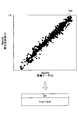
- FIG. 7 is a diagram illustrating a specific example of the processing of the relation calculation unit in the calibration phase.
- the horizontal axis represents BareSi distance data (G) acquired by the distance distribution acquisition unit 302, and the vertical axis represents BareSi relative reflectance (K) acquired by the spectrum distribution acquisition unit 301. ).
- the relation calculation unit 303 acquires data D1 and data D2, and sets a pair of BareSi distance data (G) and BareSi relative reflectance (K) measured at each of the measurement points P1 to P49. Are plotted at the positions corresponding to. Thereby, the graph 700 is generated.
- FIG. 8 is a diagram illustrating a specific example of the processing of each unit in the measurement phase.
- the spectrum distribution acquisition unit 301 acquires target reflection spectrum signals 810_1 to 810_49 of the reflected light detected by the light-collecting probe 120 at the measurement points P1 to P49 of the wafer to be measured. . Further, the spectrum distribution acquisition unit 301 notifies the correction unit 305 of the acquired target reflection spectrum signals 810_1 to 810_49.
- the distance distribution acquisition unit 302 outputs the target distance data (the distance between the light-collecting probes 120 measured by the distance sensor 130 at the measurement points P1 to P49 on the measurement target wafer, respectively). G) is notified to the parameter calculation unit 304 as distance data 820.
- the correction unit 305 subtracts the dark signal component from the target reflection spectrum signals 810_1 to 810_49 at each position of the measurement target wafer detected at each of the measurement points P1 to P49 notified from the spectrum distribution acquisition unit 301.
- the first calculation result is obtained by multiplying the subtraction result by the absolute reflectance correction coefficient Rk.
- the intensity of the target reflection spectrum signal is “Spectrum_sample” and the intensity of the dark signal is “Spectrum_dark”.
- the dark signal is a signal detected by the light collecting probe 120 in a state where the light source unit 110 does not emit visible light.
- the correction unit 305 multiplies the reference reflection spectrum signal 830 at the reference position of the reference wafer (BareSi wafer) by the corresponding relative reflectance (K), and then subtracts the dark signal component to obtain a second signal.
- a calculation result (corrected reference reflection spectrum signal) is obtained.
- the intensity of the reference reflection spectrum signal is “Spectrum_BareSi” and the intensity of the dark signal is “Spectrum_dark”.
- the correction unit 305 divides the first calculation result by the second calculation result, thereby obtaining the intensities of the target reflection spectrum signals 810_1 to 810_49 measured at the respective measurement points P1 to P49 and the corresponding corrected reference values.
- the result of comparison with the intensity of the reflection spectrum signal is obtained.
- the comparison result is “Spectrum_Cal”.
- the correction unit 305 notifies the film thickness calculation unit 160 of the intensity of the corrected reference reflection spectrum signal (“K * Spectrum_BareSi”) or the comparison result (“Spectrum_Cal”).
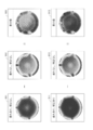
- FIG. 9 is a diagram showing that the measurement accuracy of the film thickness has been improved, and shows the result of measurement using general ellipsometry.
- a film thickness measurement result 901 is obtained by detecting reflected light in a state where the outer peripheral portion of the wafer to be measured is hung, and comparing the target reflected spectrum signal of the detected reflected light with the reference reflected spectrum signal. The result of calculating the film thickness is shown.
- the film thickness measurement result 902 indicates that the reflected light is detected in a state where the outer peripheral portion of the wafer to be measured does not hang down, and the target reflected spectrum signal of the detected reflected light is compared with the reference reflected spectrum signal. Shows the result of calculating the film thickness. By keeping the wafer to be measured in a state where there is no warpage or sagging, a film thickness measurement result 902 is obtained.
- a difference distribution 903 indicates a difference value (error in film thickness measurement) between the film thickness measurement result 901 and the film thickness measurement result 902. Specifically, FIG. 9 shows that the darker the color, the smaller the difference value, and the lighter the color, the larger the difference value. In the case of the difference distribution 903, the influence of the drooping of the outer peripheral portion of the wafer to be measured appears as an error in the film thickness measurement (the difference value is large).
- the film thickness measurement result 911 detects the reflected light in a state where the outer peripheral portion of the wafer to be measured hangs down, and compares the target reflection spectrum signal of the detected reflected light with the corrected reference reflection spectrum signal. This shows the result of calculating the film thickness.
- the film thickness measurement result 912 indicates that the reflected light is detected in a state where the outer peripheral portion of the measurement target wafer does not hang down, and the target reflection spectrum signal of the detected reflected light is compared with the reference reflection spectrum signal. This shows the result of calculating the film thickness.
- a difference distribution 913 indicates a difference value (error of the film thickness measurement) between the film thickness measurement result 911 and the film thickness measurement result 912.
- FIG. 9 shows that the darker the color, the smaller the difference value, and the lighter the color, the larger the difference value.
- the difference distribution 913 the effect of the outer peripheral portion of the wafer to be measured being drooped is eliminated, and the difference value is smaller as a whole compared with the difference distribution 903 (the error in the film thickness measurement is smaller. There).
- the corrected reference reflection spectrum signal when calculating the film thickness, it is possible to appropriately calculate the film thickness even when the outer peripheral portion of the wafer to be measured is sagging. In addition, a decrease in the measurement accuracy of the film thickness measurement can be avoided.
- the film thickness measuring apparatus has a reflection spectrum correction unit, and the reflection spectrum correction unit A reference reflection spectrum signal of the reflected light detected by the condensing probe at the reference position of the reference wafer whose thickness is known, and each reflection of the reflected light detected by the condensing probe at each position other than the reference position
- the relative reflectance of each of the spectral signals is calculated.
- a relationship between each relative reflectance and each distance data indicating a distance between each position of the reference wafer and the light-collecting probe is specified, and a linear expression is calculated.
- each relative reflectance corresponding to each distance data indicating the distance between each position of the wafer to be measured and the light-collecting probe calculates each relative reflectance corresponding to each distance data indicating the distance between each position of the wafer to be measured and the light-collecting probe.
- the reference reflection spectrum signal is corrected based on each relative reflectance calculated based on a linear expression.
- the film thickness measurement apparatus According to the film thickness measurement apparatus according to the first embodiment, even when the wafer to be measured is deformed, it is possible to appropriately calculate the film thickness, and to improve the measurement accuracy of the film thickness measurement. Drops can be avoided.
- each relative reflectance is calculated based on the peak value of the reflection spectrum signal obtained from the fluctuation range of the 49-point distance data due to the warpage or sagging of the reference wafer, and each calculated relative reflectance is calculated.
- the description has been made assuming that the relational expression is calculated using the relative reflectance.
- the method of calculating the relational expression is not limited to this.
- the peak value of the reflection spectrum signal is predicted, and the relational expression is calculated including the relative reflectance calculated based on the predicted peak value. It may be configured as follows.
- the reflected light is detected by using the deformed reference wafer.
- the method of detecting the reflected light is not limited to this.
- the reflected light may be detected while changing the distance between the focusing probe 120 and the reference wafer.
- the range of variation of the distance data can be expanded as compared with the case where a deformed reference wafer is used.
- a reference reflection spectrum signal is prepared in advance, and in the measurement phase, each time the distance data of each position of the measurement target wafer is measured, the corresponding relative reflectance is calculated. Calculated and multiplied by the reference reflection spectrum signal.
- a plurality of corrected reference reflection spectrum signals obtained by previously multiplying the reference reflection spectrum signal by the relative reflectance corresponding to each distance data may be prepared in the calibration phase. Then, in the measurement phase, every time the distance data is measured, the corresponding corrected reference reflection spectrum signal may be read.
- FIG. 8 shows the case where the correction unit 305 notifies the film thickness calculation unit 160 of the comparison result between the target reflection spectrum signal and the corrected reference reflection spectrum signal.
- the correction unit 305 may be configured to notify the corrected reference reflection spectrum signal to the film thickness calculation unit 160 and to compare the corrected reference reflection spectrum signal with the target reflection spectrum signal.
- the present invention is not limited to the configuration shown here, such as a combination of the configuration described in the above embodiment with other elements. These points can be changed without departing from the spirit of the present invention, and can be appropriately determined according to the application form.
- film thickness measuring device 110 light source unit 120: focusing probe 130: distance sensor 140: control unit 150: reflection spectrum correction unit 160: film thickness calculation unit 170: wafer chuck head 301: spectrum distribution acquisition unit 302: distance distribution Acquisition unit 303: Relation calculation unit 304: Parameter calculation unit 305: Correction unit
Landscapes
- Physics & Mathematics (AREA)
- General Physics & Mathematics (AREA)
- Health & Medical Sciences (AREA)
- Life Sciences & Earth Sciences (AREA)
- Chemical & Material Sciences (AREA)
- Analytical Chemistry (AREA)
- Biochemistry (AREA)
- General Health & Medical Sciences (AREA)
- Immunology (AREA)
- Pathology (AREA)
- Engineering & Computer Science (AREA)
- Mathematical Physics (AREA)
- Theoretical Computer Science (AREA)
- Spectroscopy & Molecular Physics (AREA)
- Length Measuring Devices By Optical Means (AREA)
- Testing Or Measuring Of Semiconductors Or The Like (AREA)
- Extrusion Moulding Of Plastics Or The Like (AREA)
Abstract
Description
膜厚が既知の第1ウェハの基準位置において、集光プローブにより検出された反射光の基準反射スペクトル信号と、基準位置以外の各位置において、該集光プローブにより検出された反射光の各反射スペクトル信号と、の各相対反射率を算出する第1算出部と、
前記第1算出部により算出された各相対反射率と、前記第1ウェハの各位置と前記集光プローブとの間の距離を示す各距離データと、の関係を特定する特定部と、
前記特定部により特定された関係に基づき、測定対象の第2ウェハの各位置と前記集光プローブとの間の距離を示す各距離データに対応する各相対反射率を算出する第2算出部と、
前記第2ウェハの各位置における膜厚を算出する際に、前記第2算出部により算出された各相対反射率に基づき、前記基準反射スペクトル信号を補正する補正部とを有する。
・測定対象のウェハの各位置における反射スペクトル信号(「対象反射スペクトル信号」)と、
・基準ウェハの反射スペクトル信号(「基準反射スペクトル信号」)と
を対比することで、各位置における膜厚を算出している。ここで、一般的な膜厚測定装置の場合、例えば、基準ウェハの中央の1点を代表値として取得し、当該点の膜厚が既知であることが前提となる。
・測定対象のウェハの各位置における反射スペクトル信号(「対象反射スペクトル信号」)と、
・測定対象のウェハの各位置の距離データに対応する各補正済み基準反射スペクトル信号と
を対比することで、各位置における膜厚を算出する。
<膜厚測定装置の構成>
図1は、膜厚測定装置の構成を示す模式図であり、膜厚測定装置が有する各構成のうちの一部の構成を抜粋して示している。図1に示すように、膜厚測定装置100は、少なくとも、光源部110と、集光プローブ120と、距離センサ130と、制御部140と、ウェハチャックヘッド170とを有する。
次に、制御部140のハードウェア構成について説明する。図2は、制御部のハードウェア構成の一例を示す図である。図2に示すように、制御部140は、CPU(Central Processing Unit)201、ROM(Read Only Memory)202、RAM(Random Access Memory)203を有する。CPU201、ROM202、RAM203は、いわゆるコンピュータを形成する。
次に、反射スペクトル補正プログラムが実行されることで実現される、反射スペクトル補正部150の機能構成の詳細について説明する。
次に、反射スペクトル補正部150による反射スペクトル補正処理の流れについて説明する。図4は、反射スペクトル補正部による反射スペクトル補正処理の流れを示すフローチャートである。なお、図4に示す反射スペクトル補正処理を開始するにあたり、反射スペクトル補正部150では、絶対反射率の補正係数(Rk)の算出が完了しているものとする。絶対反射率の補正係数(Rk)は、例えば、石英ガラスなどの標準サンプルを用いて、NIST(アメリカ国立標準技術研究所)等で発行された絶対スペクトルのデータをもとに行われる。
次に、反射スペクトル補正部150の各部(スペクトル分布取得部301、距離分布取得部302、関係算出部303)の校正フェーズでの処理の具体例について説明する。
はじめに、スペクトル分布取得部301の校正フェーズでの処理の具体例について説明する。図5は、校正フェーズにおける反射スペクトル分布取得部の処理の具体例を示す図である。
次に、距離分布取得部302の校正フェーズでの処理の具体例について説明する。図6は、校正フェーズにおける距離分布取得部の処理の具体例を示す図である。
次に、関係算出部303の校正フェーズでの処理の具体例について説明する。図7は、校正フェーズにおける関係算出部の処理の具体例を示す図である。
次に、反射スペクトル補正部150の各部の測定フェーズでの処理の具体例について説明する。図8は、測定フェーズにおける各部の処理の具体例を示す図である。
次に、補正済み基準反射スペクトル信号を用いて膜厚を算出した場合の効果について、図9を用いて説明する。図9は、膜厚の測定精度が向上したことを示す図であり、一般的なエリプソメトリを使用して計測した結果を示している。
以上の説明から明らかなように、第1の実施形態に係る膜厚測定装置は、反射スペクトル補正部を有しており、当該反射スペクトル補正部は、
・膜厚が既知の基準ウェハの基準位置において、集光プローブにより検出された反射光の基準反射スペクトル信号と、基準位置以外の各位置において、該集光プローブにより検出された反射光の各反射スペクトル信号と、の各相対反射率を算出する。
・各相対反射率と、基準ウェハの各位置と集光プローブとの間の距離を示す各距離データとの関係を特定し、一次式を算出する。
・一次式に基づき、測定対象のウェハの各位置と集光プローブとの間の距離を示す各距離データに対応する各相対反射率を算出する。
・測定対象のウェハの各位置における膜厚を算出する際に、一次式に基づいて算出された各相対反射率に基づき、基準反射スペクトル信号を補正する。
上記第1の実施形態では、基準ウェハの反りや垂れに伴う49点分の距離データの変動範囲から得られた、反射スペクトル信号のピーク値に基づいて各相対反射率を算出し、算出した各相対反射率を用いて、関係式を算出するものとして説明した。
110 :光源部
120 :集光プローブ
130 :距離センサ
140 :制御部
150 :反射スペクトル補正部
160 :膜厚算出部
170 :ウェハチャックヘッド
301 :スペクトル分布取得部
302 :距離分布取得部
303 :関係算出部
304 :パラメータ算出部
305 :補正部
Claims (7)
- 膜厚が既知の第1ウェハの基準位置において、集光プローブにより検出された反射光の基準反射スペクトル信号と、基準位置以外の各位置において、該集光プローブにより検出された反射光の各反射スペクトル信号と、の各相対反射率を算出する第1算出部と、
前記第1算出部により算出された各相対反射率と、前記第1ウェハの各位置と前記集光プローブとの間の距離を示す各距離データと、の関係を特定する特定部と、
前記特定部により特定された関係に基づき、測定対象の第2ウェハの各位置と前記集光プローブとの間の距離を示す各距離データに対応する各相対反射率を算出する第2算出部と、
前記第2ウェハの各位置における膜厚を算出する際に、前記第2算出部により算出された各相対反射率に基づき、前記基準反射スペクトル信号を補正する補正部と
を有する膜厚測定装置。 - 前記第1算出部は、
前記第1ウェハの基準位置において、集光プローブにより検出された反射光の基準反射スペクトル信号から抽出したピーク値と、前記基準位置以外の各位置において、前記集光プローブにより検出された反射光の反射スペクトル信号から抽出したピーク値と、を用いて前記各相対反射率を算出する、請求項1に記載の膜厚測定装置。 - 前記特定部は、
前記第1算出部により算出された各相対反射率と、前記第1ウェハの各位置の前記集光プローブとの間の距離を示す各距離データとの関係を、一次式で近似する、請求項2に記載の膜厚測定装置。 - 前記補正部は、
前記基準反射スペクトル信号に、算出した前記各相対反射率を乗算することで、各補正済み基準反射スペクトル信号を算出し、
前記第2ウェハの各位置において、前記集光プローブにより検出された反射光の各対象反射スペクトル信号と、前記各補正済み基準反射スペクトル信号とを対比することで対比結果を算出し、前記第2ウェハの各位置における膜厚を算出する際に用いる、請求項1に記載の膜厚測定装置。 - さらに、ウェハ上の所望の点と前記集光プローブとの間の距離を測定するための距離センサを有し、
前記第1ウェハの各位置と前記集光プローブとの間の距離を示す各距離データと、前記第2ウェハの各位置と前記集光プローブとの間の距離を示す各距離データは、前記距離センサによって取得される、
請求項1ないし4のいずれか一項に記載の膜厚測定装置。 - 前記集光プローブによる反射光の検出と前記距離センサによる距離の測定は並行して実行される、
請求項5に記載の膜厚測定装置。 - 膜厚が既知の第1ウェハの基準位置において、集光プローブにより検出された反射光の基準反射スペクトル信号と、基準位置以外の各位置において、該集光プローブにより検出された反射光の各反射スペクトル信号と、の各相対反射率を算出する第1算出工程と、
前記第1算出工程において算出された各相対反射率と、前記第1ウェハの各位置と前記集光プローブとの間の距離を示す各距離データと、の関係を特定する特定工程と、
前記特定工程において特定された関係に基づき、測定対象の第2ウェハの各位置と前記集光プローブとの間の距離を示す各距離データに対応する各相対反射率を算出する第2算出工程と、
前記第2ウェハの各位置における膜厚を算出する際に、前記第2算出工程において算出された各相対反射率に基づき、前記基準反射スペクトル信号を補正する補正工程と
を有する補正方法。
Priority Applications (4)
| Application Number | Priority Date | Filing Date | Title |
|---|---|---|---|
| US17/253,752 US11226191B2 (en) | 2018-06-27 | 2019-06-18 | Film thickness measurement device and correction method |
| CN201980041067.0A CN112334731B (zh) | 2018-06-27 | 2019-06-18 | 膜厚测定装置及校正方法 |
| JP2020527427A JP7118148B2 (ja) | 2018-06-27 | 2019-06-18 | 膜厚測定装置及び補正方法 |
| KR1020207036335A KR102690757B1 (ko) | 2018-06-27 | 2019-06-18 | 막두께 측정 장치 및 보정 방법 |
Applications Claiming Priority (2)
| Application Number | Priority Date | Filing Date | Title |
|---|---|---|---|
| JP2018122148 | 2018-06-27 | ||
| JP2018-122148 | 2018-06-27 |
Publications (1)
| Publication Number | Publication Date |
|---|---|
| WO2020004142A1 true WO2020004142A1 (ja) | 2020-01-02 |
Family
ID=68986541
Family Applications (1)
| Application Number | Title | Priority Date | Filing Date |
|---|---|---|---|
| PCT/JP2019/024088 Ceased WO2020004142A1 (ja) | 2018-06-27 | 2019-06-18 | 膜厚測定装置及び補正方法 |
Country Status (6)
| Country | Link |
|---|---|
| US (1) | US11226191B2 (ja) |
| JP (1) | JP7118148B2 (ja) |
| KR (1) | KR102690757B1 (ja) |
| CN (1) | CN112334731B (ja) |
| TW (1) | TWI807057B (ja) |
| WO (1) | WO2020004142A1 (ja) |
Cited By (2)
| Publication number | Priority date | Publication date | Assignee | Title |
|---|---|---|---|---|
| CN112556590A (zh) * | 2020-12-04 | 2021-03-26 | 北京中电科电子装备有限公司 | 一种晶圆测量装置、厚度测量方法及厚度测量装置 |
| JP2021144022A (ja) * | 2020-03-10 | 2021-09-24 | 東京エレクトロン株式会社 | 膜厚測定装置および膜厚測定方法、ならびに成膜システムおよび成膜方法 |
Families Citing this family (5)
| Publication number | Priority date | Publication date | Assignee | Title |
|---|---|---|---|---|
| CA2875522A1 (en) | 2002-08-20 | 2004-03-04 | Philera New Zealand Limited | Dosage forms and related therapies |
| KR20230056667A (ko) * | 2020-09-01 | 2023-04-27 | 오츠카덴시가부시끼가이샤 | 광학 측정 시스템, 광학 측정 방법 및 측정 프로그램 |
| CN118794359A (zh) * | 2024-09-14 | 2024-10-18 | 无锡卓海科技股份有限公司 | 一种薄膜层厚度测量方法及测量装置 |
| CN119537350B (zh) * | 2025-01-22 | 2025-07-18 | 北京特思迪半导体设备有限公司 | 单波长光束测厚参考数据库建立方法、测量方法及设备 |
| CN119501801B (zh) * | 2025-01-22 | 2025-04-25 | 北京特思迪半导体设备有限公司 | 用于晶圆薄膜抛光过程的厚度测量方法及设备 |
Citations (6)
| Publication number | Priority date | Publication date | Assignee | Title |
|---|---|---|---|---|
| JPH01124703A (ja) * | 1987-11-09 | 1989-05-17 | Kawasaki Steel Corp | 膜特性の非接触測定方法及び装置 |
| JP2000352505A (ja) * | 1999-04-05 | 2000-12-19 | Toshiba Corp | 膜厚測定方法および装置、薄膜処理装置並びに半導体装置の製造方法 |
| JP2003106816A (ja) * | 2001-10-01 | 2003-04-09 | Dainippon Printing Co Ltd | 膜厚測定方法及び装置 |
| JP2004205242A (ja) * | 2002-12-24 | 2004-07-22 | Sharp Corp | 膜厚測定装置およびこれを用いた電子部品の製造方法 |
| JP2005032740A (ja) * | 2003-07-07 | 2005-02-03 | Dainippon Screen Mfg Co Ltd | 膜形成装置および膜形成方法 |
| US20120026492A1 (en) * | 2010-07-30 | 2012-02-02 | Jimin Zhang | Detection of layer clearing using spectral monitoring |
Family Cites Families (14)
| Publication number | Priority date | Publication date | Assignee | Title |
|---|---|---|---|---|
| JP3625761B2 (ja) * | 2000-11-06 | 2005-03-02 | 東京エレクトロン株式会社 | 膜厚測定装置及びその方法 |
| JP3941432B2 (ja) | 2001-08-01 | 2007-07-04 | 凸版印刷株式会社 | 膜厚測定方法 |
| JP3962648B2 (ja) * | 2002-07-30 | 2007-08-22 | キヤノン株式会社 | ディストーション計測方法と露光装置 |
| JP4222927B2 (ja) * | 2002-09-20 | 2009-02-12 | エーエスエムエル ネザーランズ ビー.ブイ. | 少なくとも2波長を使用するリソグラフィ装置用アライメント・システム |
| JP4597946B2 (ja) | 2006-06-12 | 2010-12-15 | シャープ株式会社 | 端部傾斜角測定方法、起伏を有する被検査物の検査方法および検査装置 |
| US8679019B2 (en) | 2007-12-03 | 2014-03-25 | Bone Index Finland Oy | Method for measuring of thicknesses of materials using an ultrasound technique |
| JP5035904B2 (ja) | 2008-02-13 | 2012-09-26 | 国立大学法人名古屋大学 | 膜厚分布測定装置 |
| JP2013032981A (ja) * | 2011-08-02 | 2013-02-14 | Otsuka Denshi Co Ltd | 膜厚測定装置 |
| JP5660026B2 (ja) * | 2011-12-28 | 2015-01-28 | 信越半導体株式会社 | 膜厚分布測定方法 |
| CN103575223B (zh) * | 2012-08-09 | 2016-09-21 | 北京智朗芯光科技有限公司 | 利用反射光谱测量硅基太阳能电池增透膜的方法 |
| WO2014046156A1 (ja) * | 2012-09-24 | 2014-03-27 | コニカミノルタ株式会社 | 分子間相互作用の測定方法、光学膜厚測定方法、並びに測定システム及び測定プログラム |
| CN104567598A (zh) * | 2014-12-31 | 2015-04-29 | 彩虹(合肥)液晶玻璃有限公司 | 液晶基板玻璃成型出炉跑偏量测量装置及测量处理方法 |
| WO2017141299A1 (ja) * | 2016-02-15 | 2017-08-24 | 信越半導体株式会社 | 膜厚分布測定方法 |
| CN108225213B (zh) * | 2018-01-19 | 2019-12-17 | 北京理工大学 | 自由曲面非接触降维误差分离检测方法与装置 |
-
2019
- 2019-06-18 WO PCT/JP2019/024088 patent/WO2020004142A1/ja not_active Ceased
- 2019-06-18 KR KR1020207036335A patent/KR102690757B1/ko active Active
- 2019-06-18 US US17/253,752 patent/US11226191B2/en active Active
- 2019-06-18 JP JP2020527427A patent/JP7118148B2/ja active Active
- 2019-06-18 CN CN201980041067.0A patent/CN112334731B/zh active Active
- 2019-06-24 TW TW108121969A patent/TWI807057B/zh active
Patent Citations (6)
| Publication number | Priority date | Publication date | Assignee | Title |
|---|---|---|---|---|
| JPH01124703A (ja) * | 1987-11-09 | 1989-05-17 | Kawasaki Steel Corp | 膜特性の非接触測定方法及び装置 |
| JP2000352505A (ja) * | 1999-04-05 | 2000-12-19 | Toshiba Corp | 膜厚測定方法および装置、薄膜処理装置並びに半導体装置の製造方法 |
| JP2003106816A (ja) * | 2001-10-01 | 2003-04-09 | Dainippon Printing Co Ltd | 膜厚測定方法及び装置 |
| JP2004205242A (ja) * | 2002-12-24 | 2004-07-22 | Sharp Corp | 膜厚測定装置およびこれを用いた電子部品の製造方法 |
| JP2005032740A (ja) * | 2003-07-07 | 2005-02-03 | Dainippon Screen Mfg Co Ltd | 膜形成装置および膜形成方法 |
| US20120026492A1 (en) * | 2010-07-30 | 2012-02-02 | Jimin Zhang | Detection of layer clearing using spectral monitoring |
Cited By (3)
| Publication number | Priority date | Publication date | Assignee | Title |
|---|---|---|---|---|
| JP2021144022A (ja) * | 2020-03-10 | 2021-09-24 | 東京エレクトロン株式会社 | 膜厚測定装置および膜厚測定方法、ならびに成膜システムおよび成膜方法 |
| JP7523318B2 (ja) | 2020-03-10 | 2024-07-26 | 東京エレクトロン株式会社 | 膜厚測定装置および膜厚測定方法、ならびに成膜システムおよび成膜方法 |
| CN112556590A (zh) * | 2020-12-04 | 2021-03-26 | 北京中电科电子装备有限公司 | 一种晶圆测量装置、厚度测量方法及厚度测量装置 |
Also Published As
| Publication number | Publication date |
|---|---|
| TWI807057B (zh) | 2023-07-01 |
| TW202014668A (zh) | 2020-04-16 |
| JP7118148B2 (ja) | 2022-08-15 |
| CN112334731B (zh) | 2022-09-02 |
| KR102690757B1 (ko) | 2024-07-31 |
| US11226191B2 (en) | 2022-01-18 |
| JPWO2020004142A1 (ja) | 2021-06-24 |
| US20210270597A1 (en) | 2021-09-02 |
| KR20210024468A (ko) | 2021-03-05 |
| CN112334731A (zh) | 2021-02-05 |
Similar Documents
| Publication | Publication Date | Title |
|---|---|---|
| JP7118148B2 (ja) | 膜厚測定装置及び補正方法 | |
| JP4279322B2 (ja) | 波長選択方法、膜厚計測方法、膜厚計測装置、及び薄膜シリコン系デバイスの製造システム | |
| US6384408B1 (en) | Calibration of a scanning electron microscope | |
| US11460783B2 (en) | System and method for focus control in extreme ultraviolet lithography systems using a focus-sensitive metrology target | |
| CN110455417B (zh) | 针对红外光学系统杂散辐射的定量测量误差校正方法 | |
| CN110082074A (zh) | 一种干涉波前检测中剔除平面反射镜引入的系统误差的方法 | |
| CN116105875B (zh) | 基于背景辐射校正的偏振遥感器短波红外波段定标方法 | |
| CN113175883A (zh) | 一种光谱共焦测量系统的光源归一化处理方法 | |
| US7015447B2 (en) | Illuminance calibrating method of illuminator, illuminance calibration controller of illuminator, illuminance calibrating program of illuminator, recording medium storing the program and measuring tool | |
| KR102174505B1 (ko) | 기울기 보정기능을 갖는 필름 두께 측정시스템 | |
| CN110849827B (zh) | 中阶梯光谱仪的光谱定标方法、装置、设备及存储介质 | |
| CN116256069B (zh) | 一种双波长温度测量系统定标方法 | |
| US20240240933A1 (en) | Film thickness measurement device and film thickness measurement method | |
| CN114688964B (zh) | 关键尺寸测量校正方法、系统及计算机可读存储介质 | |
| JP5833963B2 (ja) | 明暗検査装置、明暗検査方法 | |
| JP2016003962A (ja) | 測定方法、測定装置、およびプログラム | |
| US12442774B2 (en) | Substrate inspecting apparatus and operating method thereof | |
| US20230169643A1 (en) | Monitoring of deposited or etched film thickness using image-based mass distribution metrology | |
| JP7415676B2 (ja) | 輝度計状態判定システム、輝度計状態判定装置及びプログラム | |
| JP2007057497A (ja) | 蛍光体膜厚検査システム及び蛍光体膜厚検査方法 | |
| JP2010112819A (ja) | 斜入射干渉計における測定感度の校正方法 | |
| JP2001056253A (ja) | 温度測定方法及び温度測定装置 | |
| JP2009270847A (ja) | 反射率測定装置および反射率測定方法 | |
| US10571391B2 (en) | Method for adjusting a measuring device | |
| CN119666870A (zh) | 缺陷检测设备的校准方法、装置、校准设备、产品及介质 |
Legal Events
| Date | Code | Title | Description |
|---|---|---|---|
| 121 | Ep: the epo has been informed by wipo that ep was designated in this application |
Ref document number: 19827090 Country of ref document: EP Kind code of ref document: A1 |
|
| ENP | Entry into the national phase |
Ref document number: 2020527427 Country of ref document: JP Kind code of ref document: A |
|
| ENP | Entry into the national phase |
Ref document number: 20207036335 Country of ref document: KR Kind code of ref document: A |
|
| NENP | Non-entry into the national phase |
Ref country code: DE |
|
| 122 | Ep: pct application non-entry in european phase |
Ref document number: 19827090 Country of ref document: EP Kind code of ref document: A1 |