WO2020004340A1 - Multiplexeur - Google Patents
Multiplexeur Download PDFInfo
- Publication number
- WO2020004340A1 WO2020004340A1 PCT/JP2019/024981 JP2019024981W WO2020004340A1 WO 2020004340 A1 WO2020004340 A1 WO 2020004340A1 JP 2019024981 W JP2019024981 W JP 2019024981W WO 2020004340 A1 WO2020004340 A1 WO 2020004340A1
- Authority
- WO
- WIPO (PCT)
- Prior art keywords
- filter
- phase
- phase circuit
- pass band
- impedance
- Prior art date
- Legal status (The legal status is an assumption and is not a legal conclusion. Google has not performed a legal analysis and makes no representation as to the accuracy of the status listed.)
- Ceased
Links
Images






Classifications
-
- H—ELECTRICITY
- H03—ELECTRONIC CIRCUITRY
- H03H—IMPEDANCE NETWORKS, e.g. RESONANT CIRCUITS; RESONATORS
- H03H9/00—Networks comprising electromechanical or electro-acoustic elements; Electromechanical resonators
- H03H9/74—Multiple-port networks for connecting several sources or loads, working on the same frequency or frequency band, to a common load or source
- H03H9/76—Networks using surface acoustic waves
-
- H—ELECTRICITY
- H03—ELECTRONIC CIRCUITRY
- H03H—IMPEDANCE NETWORKS, e.g. RESONANT CIRCUITS; RESONATORS
- H03H7/00—Multiple-port networks comprising only passive electrical elements as network components
- H03H7/01—Frequency selective two-port networks
- H03H7/0138—Electrical filters or coupling circuits
-
- H—ELECTRICITY
- H03—ELECTRONIC CIRCUITRY
- H03H—IMPEDANCE NETWORKS, e.g. RESONANT CIRCUITS; RESONATORS
- H03H7/00—Multiple-port networks comprising only passive electrical elements as network components
- H03H7/18—Networks for phase shifting
-
- H—ELECTRICITY
- H03—ELECTRONIC CIRCUITRY
- H03H—IMPEDANCE NETWORKS, e.g. RESONANT CIRCUITS; RESONATORS
- H03H9/00—Networks comprising electromechanical or electro-acoustic elements; Electromechanical resonators
- H03H9/70—Multiple-port networks for connecting several sources or loads, working on different frequencies or frequency bands, to a common load or source
- H03H9/72—Networks using surface acoustic waves
-
- H—ELECTRICITY
- H04—ELECTRIC COMMUNICATION TECHNIQUE
- H04B—TRANSMISSION
- H04B1/00—Details of transmission systems, not covered by a single one of groups H04B3/00 - H04B13/00; Details of transmission systems not characterised by the medium used for transmission
- H04B1/005—Details of transmission systems, not covered by a single one of groups H04B3/00 - H04B13/00; Details of transmission systems not characterised by the medium used for transmission adapting radio receivers, transmitters andtransceivers for operation on two or more bands, i.e. frequency ranges
- H04B1/0053—Details of transmission systems, not covered by a single one of groups H04B3/00 - H04B13/00; Details of transmission systems not characterised by the medium used for transmission adapting radio receivers, transmitters andtransceivers for operation on two or more bands, i.e. frequency ranges with common antenna for more than one band
- H04B1/0057—Details of transmission systems, not covered by a single one of groups H04B3/00 - H04B13/00; Details of transmission systems not characterised by the medium used for transmission adapting radio receivers, transmitters andtransceivers for operation on two or more bands, i.e. frequency ranges with common antenna for more than one band using diplexing or multiplexing filters for selecting the desired band
-
- H—ELECTRICITY
- H03—ELECTRONIC CIRCUITRY
- H03H—IMPEDANCE NETWORKS, e.g. RESONANT CIRCUITS; RESONATORS
- H03H7/00—Multiple-port networks comprising only passive electrical elements as network components
- H03H7/46—Networks for connecting several sources or loads, working on different frequencies or frequency bands, to a common load or source
Definitions
- the present disclosure relates to a multiplexer, and more specifically, to a configuration of a multiplexer that reduces the influence of an unnecessary wave (spurious) generated in a filter.
- multi-band communication for performing communication using radio waves in a plurality of frequency bands has been promoted in mobile terminals such as mobile phones and smartphones.
- a multiplexer for dividing a high-frequency signal transmitted and received by one antenna into signals in a plurality of frequency bands is mounted.
- Patent Document 1 JP-A-2013-62556 discloses a multiplexer including a plurality of band-pass filters having different pass bands.
- Patent Document 1 discloses a configuration in which a duplexer in which two filters (F1 and F2) are connected in parallel and another filter are connected in parallel to an antenna terminal via a matching circuit. In each filter, the matching circuit is adjusted such that the impedance phase in the pass band of the other filter is open when viewed from the antenna terminal.
- a sudden phase change occurs due to the influence of external noise or the like, and an unnecessary wave (spurious) which is a frequency signal component other than a predetermined frequency may be generated.
- an unnecessary wave which is a frequency signal component other than a predetermined frequency
- the influence of the spurious generated in the filter A is transmitted to the filter B, which may lead to deterioration of the pass characteristic of the filter B. is there.
- the present disclosure has been made in order to solve such a problem, and an object of the present disclosure is to provide a multiplexer including a plurality of band-pass filters having different pass bands from each other in order to suppress the deterioration of the pass characteristics due to generation of spurious. It is to suppress.
- a multiplexer includes an antenna terminal, first to third filters, and first and second phase circuits configured to adjust phases of passing signals.
- the first filter has a first pass band and is connected to an antenna terminal.
- the second filter has a second pass band and is connected to the antenna terminal via the first phase circuit.
- the second filter generates an unnecessary wave in the first pass band.
- the third filter has a third pass band, and is connected to a connection node between the first phase circuit and the second filter via the second phase circuit.
- the first phase circuit adjusts the phase so that the impedance of the first pass band at the antenna terminal is in an open state.
- the second phase circuit adjusts the phase so that the impedance of the first pass band at the connection node is in a short state.
- the second filter in which spurious is generated in the first pass band is connected to the first filter via the first phase circuit adjusted so that the impedance of the first pass band is in an open state.
- it is connected to the third filter via a second phase circuit adjusted so that the impedance of the first pass band is in a short-circuit state. Therefore, the spurious generated in the second filter is not transmitted to the first filter having the first pass band, but is transmitted to the third filter. Therefore, it is possible to prevent the pass characteristics of the first filter from being deteriorated due to the influence of spurious components generated in the second filter.
- FIG. 3 is a schematic circuit diagram of a multiplexer according to an embodiment. It is a figure for explaining generation of a spurious.
- FIG. 9 is a diagram for explaining a phase change by a second phase circuit.
- FIG. 9 is a diagram for explaining the phases of the second filter and the third filter at the junction of the second filter and the third filter.
- FIG. 4 is a diagram illustrating an example of a second phase circuit.
- FIG. 4 is a diagram for explaining a phase change by a first phase circuit.
- FIG. 3 is a diagram illustrating an example of a first phase circuit.
- FIG. 7 is a diagram for explaining an influence of a spurious generated by a second filter on a first filter due to the presence or absence of a phase circuit;
- FIG. 9 is a diagram for explaining a relationship between a spurious level generated in a second filter and an adjustment range of a second phase circuit.
- FIG. 7 is a diagram illustrating an example of an adjustment range of a second phase circuit with respect
- FIG. 1 is a schematic circuit diagram of a multiplexer 1 according to the present embodiment.
- multiplexer 1 includes an antenna terminal T0 to which antenna ANT is connected, filters 10 to 30, phase circuits 40 and 45, and output terminals T1 to T3.
- the filters 10 to 30 are band-pass filters having different pass bands.
- a surface acoustic wave (Surface Acoustic Wave) (SAW) filter or a bulk acoustic wave (Bulk Acoustic Wave) (BAW) filter can be used.
- the filter 10 (first filter) has a pass band BW1 (first pass band), the filter 20 (second filter) has a pass band BW2 (second pass band), and the filter 30 (third filter) It has a pass band BW3 (third pass band).
- the pass band of each filter can be set arbitrarily.
- the pass band BW1 is located at the lowest frequency band, and the pass band BW3 is located at the highest frequency.
- Band, and the passband BW2 is set so as to be located in an intermediate frequency band.
- the filter 10 is connected to the antenna terminal T0, and allows the signal in the pass band BW1 of the high-frequency signal received by the antenna ANT to pass to the output terminal T1.
- the filter 20 is connected to the antenna terminal T0 via the phase circuit 40 (first phase circuit).
- the filter 20 allows the signal in the pass band BW2 among the high-frequency signals received by the antenna ANT to pass to the output terminal T2.
- the filter 30 is connected to a connection node JP2 between the phase circuit 40 and the filter 20 via the phase circuit 45 (second phase circuit).
- the filter 30 allows the signal in the pass band BW3 of the high-frequency signal received by the antenna ANT to pass to the output terminal T3.
- the multiplexer 1 has a configuration in which the filters 20 and 30 connected in parallel via the phase circuit 45 are connected in parallel with the filter 10 via the phase circuit 40.
- the phase circuits 40 and 45 are circuits for adjusting the phase of the high-frequency signal passing therethrough.
- the phase circuit 40 passes the filter 10 such that the impedance of the passband (passband BW1) of the filter 10 at the connection node JP1 (that is, the antenna terminal T0) between the filter 10 and the duplexer is open. Adjust the signal phase.
- the phase circuit 45 adjusts the phase of the pass signal so that the impedance of the pass band BW1 at the connection node JP2 is in a short-circuit state.
- the “open state” of the impedance means a high impedance state, and indicates a state in which the phase is near the left end (around ⁇ 180 °) in the Smith chart. .
- the “open state” does not necessarily mean that the impedance is infinite.
- the “short state” in the impedance means a low impedance state in which the impedance is close to 0 ⁇ , and indicates a state in which the phase is near the right end (near 0 °) in the Smith chart.
- each filter when viewed from the antenna terminal T0, each filter is in a short-circuit state with respect to a signal having a frequency corresponding to its own pass band, and is in a short-circuit state with respect to a signal having a frequency other than the pass band. Is set to the open state.
- an unnecessary wave (spurious) having a frequency other than its own pass band may occur due to the influence of noise or the like. If the frequency of this spurious is included in the pass band of another filter, it may affect the pass characteristics of the other filter.
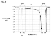
- FIG. 2 is a diagram for explaining the generation of spurious components, and shows an example in which spurious components having a frequency within the pass band BW1 of the filter 10 are generated in the filter 20 having the configuration shown in FIG. More specifically, in FIG. 2, the horizontal axis represents frequency, and the vertical axis represents reflection loss (return loss) of the filter 20 at the antenna terminal T0.
- the impedance is low and the return loss is large, and the signal in the pass band BW2 is passed with low loss. It is supposed to.
- the return loss should be low originally, but the return loss is slightly large at the frequency fa due to the influence of spurious.
- the spurious generated in the filter 20 is transmitted to the filter 10 through the connection node JP1 as indicated by a broken line arrow RT in FIG. Will be done. Since the spurious frequency is within the pass band BW1 of the filter 10, the spurious passes through the filter 10 and is output from the output terminal T1, and as a result, the pass characteristic of the filter 10 is deteriorated.
- the phase is adjusted by phase circuit 40 so that the impedance of passband BW1 at antenna terminal T0 (that is, connection node JP1) is in an open state.
- the phase is adjusted so that the impedance of the pass band BW1 in is short-circuited.
- the impedance of the pass band BW1 of the phase circuit 40 since the impedance of the pass band BW1 of the phase circuit 40 is in an open state, the signal of the pass band BW1 in the high frequency signal received by the antenna ANT does not flow to the filters 20 and 30, but flows to the filter 10. . As a result, it is possible to suppress a decrease in the pass characteristics of the filter 10.
- FIG. 3 is a diagram for explaining the phase of the pass band BW1 of the filter 30 after passing through the phase circuit 45.
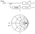
- the phase circuit 45 is adjusted so that the impedance of the filter 10 with respect to the pass band BW1 is in a short-circuit state. Therefore, in the Smith chart of FIG. The impedance is located near the area AR1) in the drawing.
- FIG. 4 illustrates the phase of the signal in the passband BW1 when the filters 20 and 30 are viewed from the connection node JP2 when the filters 20 and 30 are connected (FIG. 4A).
- FIG. In this case, the connection node JP2 is directly connected to the filter 20, and the phase of the phase circuit 45 is adjusted so that the impedance of the pass band BW1 is in a short-circuit state. Therefore, when the filters 20 and 30 are viewed from the connection node JP2, the impedance of the pass band BW1 is short-circuited as a whole, and as shown in FIG. The impedance is located near (the area AR1 in the figure).
- FIG. 5 is a diagram showing an example of a specific circuit configuration for realizing the phase circuit 45.
- the phase circuit 45 includes a delay line 60 (FIG. 5A), a series inductor L1 (FIG. 5B), a parallel capacitor C1 (FIG. 5C), and a combination of the series inductor L1 and the parallel capacitor C1. Any of the combinations (FIG. 5D) can be applied.
- FIG. 5A shows an example in which the delay line 60 is applied as the phase circuit 45.
- the delay line moves the impedance clockwise along a circle (equal SWR circle) centered on the center of the Smith chart. Therefore, by adjusting the length of the delay line, the impedance can be made closer to the short-circuited region AR2 in FIG. 4B.
- a series inductor L1 can be applied as shown in FIG.
- the series inductor moves the impedance clockwise along a circle (equiresistance circle) that touches the right end of the Smith chart. Therefore, by adjusting the inductance of the series inductor L1, the impedance can be brought closer to the short-circuited area AR2 in FIG. 4B.
- a parallel capacitor C1 can be applied as shown in FIG.
- the parallel capacitor moves the impedance clockwise along a circle (equiconductance circle) tangent to the left end of the Smith chart. Therefore, by adjusting the capacitance of the parallel capacitor C1, the impedance can be made closer to the short-circuited area AR2 in FIG. 4B.
- FIG. 5D shows an example in which the above-described series inductor L1 and parallel capacitor C1 are combined.
- the phase is adjusted only with the series inductor or only the parallel capacitor, it may not be possible to approach the short-circuit state sufficiently, or the element size of the inductor and capacitor used may need to be increased. May occur.
- the delay line 60 may be further combined in addition to the series inductor L1 and the parallel capacitor C1.
- FIG. 6 is a diagram for explaining the phase of the pass band BW1 of the filters 20 and 30 after passing through the phase circuit 40. That is, as shown in FIG. 6A, when the filters 20 and 30 are viewed from the connection node JP1, the impedance of the signal in the pass band BW1 is described. As described above, the phase circuit 40 is adjusted so that the impedance of the filter 10 with respect to the pass band BW1 is in an open state. Therefore, in the Smith chart of FIG. The impedance is located near the area AR3) in the drawing. As a result, spurious components having a frequency within the pass band BW1 generated by the filter 20 cannot pass through the phase circuit 40 but flow through the low impedance phase circuit 45 to the filter 30 side. Therefore, it is possible to prevent the spurious generated in the filter 20 from being transmitted to the filter 10.
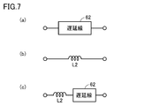
- FIG. 7 is a diagram showing an example of a specific circuit configuration for implementing the phase circuit 40.
- a delay line 62 (FIG. 7A), a series inductor L2 (FIG. 7B), and a combination of the delay line 62 and the series inductor L2 (FIG. 7C) are applied.
- the use of the delay line causes the impedance to move clockwise along the equal SWR circle
- the use of the series inductor causes the impedance to move clockwise along the equal resistance circle. Therefore, when the initial impedance is the capacitive impedance located in the lower half of the Smith chart, the phase is changed more greatly than in the case of the short-circuit state shown in FIG.
- the inductance of the series inductor L2 used for the phase circuit 40 is made larger than the inductance of the series inductor L1 used for the phase circuit 45.
- FIG. 8 is a diagram for explaining the influence of the presence or absence of the phase circuits 40 and 45 on the filter 10 due to the spurious generated in the filter 20. Specifically, FIG. 8 compares the insertion loss of the filter 10 in the case of the multiplexer (comparative example) not using the phase circuits 40 and 45 with the insertion loss of the filter 10 in the case of the multiplexer 1 of the present embodiment. This is a simulation result.
- a broken line LN2 indicates the insertion loss in the case of the comparative example
- a solid line LN3 indicates the insertion loss in the case of the present embodiment.
- FIG. 9 is a diagram for explaining the relationship between the level of spurious generated by the filter 20 and the adjustment range of the phase circuit 45.
- the horizontal axis of FIG. 9 shows the phase after passing through the phase circuit 45, and the vertical axis shows the return loss of the filters 20, 30 when the filters 20, 30 are viewed from the connection node JP1.
- Lines LN10 to LN50 show the case where the return loss of spurious (ripple) generated in the filter 20 is 1 dB, 3 dB, 5 dB, 10 dB, and 30 dB, respectively.
- the spurious level increases as the decibel value of the return loss increases.
- the allowable value of the return loss is set to 1 dB (line ALW), and the state in which the return loss is smaller than the allowable value (that is, the upper side of the line ALW in FIG. 9) is affected by the spurious effect on the filter 10. Has been reduced.
- the spurious return loss is as small as 1 dB (line LN10)
- the phase is adjusted within the range of ⁇ 235 ° or more and less than ⁇ 15 ° using the phase circuit 45, the filter 10 due to the spurious generated in the filter 20 can be obtained. It has been shown that the effect on the water can be reduced to an acceptable range.
- phase circuit 45 When the return loss of spurious is as large as 30 dB (line LN50), in order to reduce the influence of spurious to an allowable range, the phase is adjusted by the phase circuit 45 to a narrower range from -200 ° to less than -155 °. Has been shown to be necessary.
- the adjustment range of the phase by the phase circuit 45 decreases.
- the spurious level increases, it is necessary to adjust the phase to a greater extent in order to reduce the influence of the spurious to an allowable range.
- FIG. 10 is a diagram showing an example of an adjustment range of the phase circuit 45 with respect to a spurious level.
- the adjustment range is determined based on the result of the simulation shown in FIG.
- phase circuit 45 causes the return loss to be ⁇ 200 ° or more and less than ⁇ 155 °.
- the influence of spurious on the filter 10 can be reduced to an allowable range.
- the phase adjustment range of the phase circuit 45 is -205 ° or more and less than -145 °.
- the phase adjustment range of the phase circuit 45 is ⁇ 210 ° or more and less than ⁇ 130 °.
- the phase adjustment range of the phase circuit 45 is -215 ° or more and less than -105 °.
- phase circuit 60, 62 delay line, ALW, LN1, LN10 to LN50 line, ANT antenna, AR1 to AR3 region, BW1 to BW3 pass band, C1 capacitor, JP1, JP2 connection node, L1, L2 series inductor, T0 antenna terminal, T1 to T3 output terminal.
Landscapes
- Physics & Mathematics (AREA)
- Acoustics & Sound (AREA)
- Engineering & Computer Science (AREA)
- Computer Networks & Wireless Communication (AREA)
- Signal Processing (AREA)
- Control Of Motors That Do Not Use Commutators (AREA)
- Surface Acoustic Wave Elements And Circuit Networks Thereof (AREA)
- Transceivers (AREA)
Abstract
La présente invention concerne un multiplexeur (1) qui comprend une première borne d'antenne (ANT), des filtres (10S30) qui ont des bandes passantes différentes, et des circuits de phase (40, 45) qui règlent les phases de signaux de passage. Le filtre (10) est connecté à la borne d'antenne (ANT). Un second filtre (20) est connecté à la borne d'antenne (ANT) par l'intermédiaire d'un circuit de phase (40). Le filtre (30) est connecté à un point de jonction (JP2) par l'intermédiaire d'un circuit de phase (45). Des ondes non nécessaires se produisent au niveau du filtre (20) dans une première bande passante de filtre (10). Le circuit de phase (40) effectue un réglage de phase de telle sorte que l'impédance au niveau de la borne d'antenne (ANT) pour la première bande passante soit dans un état ouvert. Le circuit de phase (45) effectue un réglage de phase de telle sorte que l'impédance au niveau du point de jonction (JP2) pour la première bande passante soit dans un état court-circuité.
Priority Applications (2)
| Application Number | Priority Date | Filing Date | Title |
|---|---|---|---|
| CN201980043301.3A CN112335177B (zh) | 2018-06-29 | 2019-06-24 | 多工器 |
| US17/108,042 US11444594B2 (en) | 2018-06-29 | 2020-12-01 | Multiplexer |
Applications Claiming Priority (2)
| Application Number | Priority Date | Filing Date | Title |
|---|---|---|---|
| JP2018124079 | 2018-06-29 | ||
| JP2018-124079 | 2018-06-29 |
Related Child Applications (1)
| Application Number | Title | Priority Date | Filing Date |
|---|---|---|---|
| US17/108,042 Continuation US11444594B2 (en) | 2018-06-29 | 2020-12-01 | Multiplexer |
Publications (1)
| Publication Number | Publication Date |
|---|---|
| WO2020004340A1 true WO2020004340A1 (fr) | 2020-01-02 |
Family
ID=68987078
Family Applications (1)
| Application Number | Title | Priority Date | Filing Date |
|---|---|---|---|
| PCT/JP2019/024981 Ceased WO2020004340A1 (fr) | 2018-06-29 | 2019-06-24 | Multiplexeur |
Country Status (3)
| Country | Link |
|---|---|
| US (1) | US11444594B2 (fr) |
| CN (1) | CN112335177B (fr) |
| WO (1) | WO2020004340A1 (fr) |
Cited By (1)
| Publication number | Priority date | Publication date | Assignee | Title |
|---|---|---|---|---|
| CN113506963A (zh) * | 2021-06-09 | 2021-10-15 | 电子科技大学 | 一种基于vo2的多功能滤波器 |
Families Citing this family (1)
| Publication number | Priority date | Publication date | Assignee | Title |
|---|---|---|---|---|
| US11588506B2 (en) * | 2020-04-05 | 2023-02-21 | Skyworks Solutions, Inc. | Architectures having bridge combiners and multiplexers |
Citations (3)
| Publication number | Priority date | Publication date | Assignee | Title |
|---|---|---|---|---|
| JP2007266897A (ja) * | 2006-03-28 | 2007-10-11 | Kyocera Corp | 分波器 |
| JP2009033733A (ja) * | 2007-06-29 | 2009-02-12 | Nippon Dempa Kogyo Co Ltd | アンテナ分波器 |
| JP2018019392A (ja) * | 2016-07-15 | 2018-02-01 | 株式会社村田製作所 | 高周波フロントエンド回路および通信装置 |
Family Cites Families (6)
| Publication number | Priority date | Publication date | Assignee | Title |
|---|---|---|---|---|
| CN100530958C (zh) * | 2003-10-16 | 2009-08-19 | 京瓷株式会社 | 复合型分波电路、用其的芯片零件、高频模块及无线通信设备 |
| DE102004053319A1 (de) * | 2004-11-04 | 2006-05-11 | Epcos Ag | Frequenzweiche |
| JP4842245B2 (ja) * | 2007-11-21 | 2011-12-21 | 株式会社ヨコオ | トリプレクサ回路 |
| JP2013062556A (ja) | 2010-01-13 | 2013-04-04 | Murata Mfg Co Ltd | マルチプレクサ |
| GB2526197B (en) | 2014-04-11 | 2020-11-18 | Skyworks Solutions Inc | Circuits and methods related to radio-frequency receivers having carrier aggregation |
| US9998097B2 (en) | 2016-07-15 | 2018-06-12 | Murata Manufacturing Co., Ltd. | Radio-frequency front-end circuit and communication device |
-
2019
- 2019-06-24 WO PCT/JP2019/024981 patent/WO2020004340A1/fr not_active Ceased
- 2019-06-24 CN CN201980043301.3A patent/CN112335177B/zh active Active
-
2020
- 2020-12-01 US US17/108,042 patent/US11444594B2/en active Active
Patent Citations (3)
| Publication number | Priority date | Publication date | Assignee | Title |
|---|---|---|---|---|
| JP2007266897A (ja) * | 2006-03-28 | 2007-10-11 | Kyocera Corp | 分波器 |
| JP2009033733A (ja) * | 2007-06-29 | 2009-02-12 | Nippon Dempa Kogyo Co Ltd | アンテナ分波器 |
| JP2018019392A (ja) * | 2016-07-15 | 2018-02-01 | 株式会社村田製作所 | 高周波フロントエンド回路および通信装置 |
Cited By (2)
| Publication number | Priority date | Publication date | Assignee | Title |
|---|---|---|---|---|
| CN113506963A (zh) * | 2021-06-09 | 2021-10-15 | 电子科技大学 | 一种基于vo2的多功能滤波器 |
| CN113506963B (zh) * | 2021-06-09 | 2022-07-29 | 电子科技大学 | 一种基于vo2的多功能滤波器 |
Also Published As
| Publication number | Publication date |
|---|---|
| US11444594B2 (en) | 2022-09-13 |
| CN112335177B (zh) | 2021-11-26 |
| CN112335177A (zh) | 2021-02-05 |
| US20210083642A1 (en) | 2021-03-18 |
Similar Documents
| Publication | Publication Date | Title |
|---|---|---|
| US9509279B2 (en) | Elastic wave filter with magnetically coupled LC parallel resonance circuits | |
| US10148297B2 (en) | Splitter | |
| US10224899B2 (en) | High-frequency filter, front-end circuit, and communication device | |
| KR20190112114A (ko) | 멀티플렉서, 고주파 프론트 엔드 회로 및 통신 장치 | |
| JP2009130831A (ja) | チューナブルフィルタ | |
| US9780760B2 (en) | Variable filter circuit and wireless communication apparatus | |
| US20140354512A1 (en) | Tunable filter device | |
| US9419582B2 (en) | Filter device and duplexer | |
| WO2020004340A1 (fr) | Multiplexeur | |
| KR101443963B1 (ko) | 전자 부품 | |
| JPWO2015119179A1 (ja) | 可変フィルタ回路および無線通信装置 | |
| US11290076B2 (en) | Amplifier circuit, front-end circuit, and receiver circuit | |
| JP2005295316A (ja) | リングフィルタ及びそれを用いた広帯域の帯域通過フィルタ | |
| WO2018159205A1 (fr) | Dispositif formant filtre, multiplexeur, circuit frontal à haute fréquence et appareil de communication | |
| CN112217494A (zh) | 发送滤波器电路以及复合滤波器装置 | |
| JP2021010062A (ja) | エクストラクタ | |
| CN114244312A (zh) | 一种fbar滤波器电路结构 | |
| US12040780B2 (en) | Band-stop filter and multi-frequency band-stop filter | |
| US12431854B2 (en) | Composite acoustic wave filter device | |
| JP2007209024A (ja) | 弾性表面波フィルタ | |
| WO2022227347A1 (fr) | Filtre coupe-bande et filtre coupe-bande multifréquence | |
| US20230283260A1 (en) | Notch filter and multi-frequency notch filter | |
| KR101643582B1 (ko) | If 대역 통과 필터 | |
| KR200393866Y1 (ko) | 주파수 대역 편파 감쇄기 | |
| KR20230040194A (ko) | 광대역 필터 |
Legal Events
| Date | Code | Title | Description |
|---|---|---|---|
| 121 | Ep: the epo has been informed by wipo that ep was designated in this application |
Ref document number: 19826823 Country of ref document: EP Kind code of ref document: A1 |
|
| NENP | Non-entry into the national phase |
Ref country code: DE |
|
| 122 | Ep: pct application non-entry in european phase |
Ref document number: 19826823 Country of ref document: EP Kind code of ref document: A1 |
|
| NENP | Non-entry into the national phase |
Ref country code: JP |