WO2020004459A1 - Electronic element mounting substrate, electronic device, and electronic module - Google Patents
Electronic element mounting substrate, electronic device, and electronic module Download PDFInfo
- Publication number
- WO2020004459A1 WO2020004459A1 PCT/JP2019/025369 JP2019025369W WO2020004459A1 WO 2020004459 A1 WO2020004459 A1 WO 2020004459A1 JP 2019025369 W JP2019025369 W JP 2019025369W WO 2020004459 A1 WO2020004459 A1 WO 2020004459A1
- Authority
- WO
- WIPO (PCT)
- Prior art keywords
- substrate
- electronic element
- main surface
- view
- electronic
- Prior art date
- Legal status (The legal status is an assumption and is not a legal conclusion. Google has not performed a legal analysis and makes no representation as to the accuracy of the status listed.)
- Ceased
Links
Images


Classifications
-
- H—ELECTRICITY
- H10—SEMICONDUCTOR DEVICES; ELECTRIC SOLID-STATE DEVICES NOT OTHERWISE PROVIDED FOR
- H10W—GENERIC PACKAGES, INTERCONNECTIONS, CONNECTORS OR OTHER CONSTRUCTIONAL DETAILS OF DEVICES COVERED BY CLASS H10
- H10W40/00—Arrangements for thermal protection or thermal control
- H10W40/20—Arrangements for cooling
- H10W40/22—Arrangements for cooling characterised by their shape, e.g. having conical or cylindrical projections
- H10W40/226—Arrangements for cooling characterised by their shape, e.g. having conical or cylindrical projections characterised by projecting parts, e.g. fins to increase surface area
- H10W40/228—Arrangements for cooling characterised by their shape, e.g. having conical or cylindrical projections characterised by projecting parts, e.g. fins to increase surface area the projecting parts being wire-shaped or pin-shaped
-
- H—ELECTRICITY
- H10—SEMICONDUCTOR DEVICES; ELECTRIC SOLID-STATE DEVICES NOT OTHERWISE PROVIDED FOR
- H10W—GENERIC PACKAGES, INTERCONNECTIONS, CONNECTORS OR OTHER CONSTRUCTIONAL DETAILS OF DEVICES COVERED BY CLASS H10
- H10W40/00—Arrangements for thermal protection or thermal control
- H10W40/20—Arrangements for cooling
- H10W40/22—Arrangements for cooling characterised by their shape, e.g. having conical or cylindrical projections
-
- H—ELECTRICITY
- H05—ELECTRIC TECHNIQUES NOT OTHERWISE PROVIDED FOR
- H05K—PRINTED CIRCUITS; CASINGS OR CONSTRUCTIONAL DETAILS OF ELECTRIC APPARATUS; MANUFACTURE OF ASSEMBLAGES OF ELECTRICAL COMPONENTS
- H05K1/00—Printed circuits
- H05K1/02—Details
- H05K1/03—Use of materials for the substrate
- H05K1/0306—Inorganic insulating substrates, e.g. ceramic, glass
-
- H—ELECTRICITY
- H10—SEMICONDUCTOR DEVICES; ELECTRIC SOLID-STATE DEVICES NOT OTHERWISE PROVIDED FOR
- H10W—GENERIC PACKAGES, INTERCONNECTIONS, CONNECTORS OR OTHER CONSTRUCTIONAL DETAILS OF DEVICES COVERED BY CLASS H10
- H10W40/00—Arrangements for thermal protection or thermal control
- H10W40/20—Arrangements for cooling
- H10W40/25—Arrangements for cooling characterised by their materials
-
- H—ELECTRICITY
- H10—SEMICONDUCTOR DEVICES; ELECTRIC SOLID-STATE DEVICES NOT OTHERWISE PROVIDED FOR
- H10W—GENERIC PACKAGES, INTERCONNECTIONS, CONNECTORS OR OTHER CONSTRUCTIONAL DETAILS OF DEVICES COVERED BY CLASS H10
- H10W70/00—Package substrates; Interposers; Redistribution layers [RDL]
- H10W70/60—Insulating or insulated package substrates; Interposers; Redistribution layers
- H10W70/611—Insulating or insulated package substrates; Interposers; Redistribution layers for connecting multiple chips together
-
- H—ELECTRICITY
- H10—SEMICONDUCTOR DEVICES; ELECTRIC SOLID-STATE DEVICES NOT OTHERWISE PROVIDED FOR
- H10W—GENERIC PACKAGES, INTERCONNECTIONS, CONNECTORS OR OTHER CONSTRUCTIONAL DETAILS OF DEVICES COVERED BY CLASS H10
- H10W70/00—Package substrates; Interposers; Redistribution layers [RDL]
- H10W70/60—Insulating or insulated package substrates; Interposers; Redistribution layers
- H10W70/62—Insulating or insulated package substrates; Interposers; Redistribution layers characterised by their interconnections
- H10W70/63—Vias, e.g. via plugs
- H10W70/635—Through-vias
-
- H—ELECTRICITY
- H10—SEMICONDUCTOR DEVICES; ELECTRIC SOLID-STATE DEVICES NOT OTHERWISE PROVIDED FOR
- H10W—GENERIC PACKAGES, INTERCONNECTIONS, CONNECTORS OR OTHER CONSTRUCTIONAL DETAILS OF DEVICES COVERED BY CLASS H10
- H10W70/00—Package substrates; Interposers; Redistribution layers [RDL]
- H10W70/60—Insulating or insulated package substrates; Interposers; Redistribution layers
- H10W70/67—Insulating or insulated package substrates; Interposers; Redistribution layers characterised by their insulating layers or insulating parts
- H10W70/68—Shapes or dispositions thereof
-
- H—ELECTRICITY
- H10—SEMICONDUCTOR DEVICES; ELECTRIC SOLID-STATE DEVICES NOT OTHERWISE PROVIDED FOR
- H10W—GENERIC PACKAGES, INTERCONNECTIONS, CONNECTORS OR OTHER CONSTRUCTIONAL DETAILS OF DEVICES COVERED BY CLASS H10
- H10W70/00—Package substrates; Interposers; Redistribution layers [RDL]
- H10W70/60—Insulating or insulated package substrates; Interposers; Redistribution layers
- H10W70/67—Insulating or insulated package substrates; Interposers; Redistribution layers characterised by their insulating layers or insulating parts
- H10W70/69—Insulating materials thereof
- H10W70/692—Ceramics or glasses
-
- H—ELECTRICITY
- H10—SEMICONDUCTOR DEVICES; ELECTRIC SOLID-STATE DEVICES NOT OTHERWISE PROVIDED FOR
- H10W—GENERIC PACKAGES, INTERCONNECTIONS, CONNECTORS OR OTHER CONSTRUCTIONAL DETAILS OF DEVICES COVERED BY CLASS H10
- H10W90/00—Package configurations
- H10W90/401—Package configurations characterised by multiple insulating or insulated package substrates, interposers or RDLs
-
- H—ELECTRICITY
- H05—ELECTRIC TECHNIQUES NOT OTHERWISE PROVIDED FOR
- H05K—PRINTED CIRCUITS; CASINGS OR CONSTRUCTIONAL DETAILS OF ELECTRIC APPARATUS; MANUFACTURE OF ASSEMBLAGES OF ELECTRICAL COMPONENTS
- H05K1/00—Printed circuits
- H05K1/02—Details
- H05K1/0201—Thermal arrangements, e.g. for cooling, heating or preventing overheating
- H05K1/0203—Cooling of mounted components
- H05K1/0204—Cooling of mounted components using means for thermal conduction connection in the thickness direction of the substrate
-
- H—ELECTRICITY
- H05—ELECTRIC TECHNIQUES NOT OTHERWISE PROVIDED FOR
- H05K—PRINTED CIRCUITS; CASINGS OR CONSTRUCTIONAL DETAILS OF ELECTRIC APPARATUS; MANUFACTURE OF ASSEMBLAGES OF ELECTRICAL COMPONENTS
- H05K1/00—Printed circuits
- H05K1/02—Details
- H05K1/03—Use of materials for the substrate
-
- H—ELECTRICITY
- H05—ELECTRIC TECHNIQUES NOT OTHERWISE PROVIDED FOR
- H05K—PRINTED CIRCUITS; CASINGS OR CONSTRUCTIONAL DETAILS OF ELECTRIC APPARATUS; MANUFACTURE OF ASSEMBLAGES OF ELECTRICAL COMPONENTS
- H05K1/00—Printed circuits
- H05K1/02—Details
- H05K1/11—Printed elements for providing electric connections to or between printed circuits
- H05K1/111—Pads for surface mounting, e.g. lay-out
- H05K1/112—Pads for surface mounting, e.g. lay-out directly combined with via connections
- H05K1/113—Via provided in pad; Pad over filled via
-
- H—ELECTRICITY
- H05—ELECTRIC TECHNIQUES NOT OTHERWISE PROVIDED FOR
- H05K—PRINTED CIRCUITS; CASINGS OR CONSTRUCTIONAL DETAILS OF ELECTRIC APPARATUS; MANUFACTURE OF ASSEMBLAGES OF ELECTRICAL COMPONENTS
- H05K2201/00—Indexing scheme relating to printed circuits covered by H05K1/00
- H05K2201/03—Conductive materials
- H05K2201/032—Materials
- H05K2201/0323—Carbon
-
- H—ELECTRICITY
- H05—ELECTRIC TECHNIQUES NOT OTHERWISE PROVIDED FOR
- H05K—PRINTED CIRCUITS; CASINGS OR CONSTRUCTIONAL DETAILS OF ELECTRIC APPARATUS; MANUFACTURE OF ASSEMBLAGES OF ELECTRICAL COMPONENTS
- H05K2201/00—Indexing scheme relating to printed circuits covered by H05K1/00
- H05K2201/09—Shape and layout
- H05K2201/09209—Shape and layout details of conductors
- H05K2201/095—Conductive through-holes or vias
- H05K2201/09618—Via fence, i.e. one-dimensional array of vias
-
- H—ELECTRICITY
- H05—ELECTRIC TECHNIQUES NOT OTHERWISE PROVIDED FOR
- H05K—PRINTED CIRCUITS; CASINGS OR CONSTRUCTIONAL DETAILS OF ELECTRIC APPARATUS; MANUFACTURE OF ASSEMBLAGES OF ELECTRICAL COMPONENTS
- H05K2201/00—Indexing scheme relating to printed circuits covered by H05K1/00
- H05K2201/10—Details of components or other objects attached to or integrated in a printed circuit board
- H05K2201/10007—Types of components
- H05K2201/10106—Light emitting diode [LED]
-
- H—ELECTRICITY
- H05—ELECTRIC TECHNIQUES NOT OTHERWISE PROVIDED FOR
- H05K—PRINTED CIRCUITS; CASINGS OR CONSTRUCTIONAL DETAILS OF ELECTRIC APPARATUS; MANUFACTURE OF ASSEMBLAGES OF ELECTRICAL COMPONENTS
- H05K2201/00—Indexing scheme relating to printed circuits covered by H05K1/00
- H05K2201/10—Details of components or other objects attached to or integrated in a printed circuit board
- H05K2201/10007—Types of components
- H05K2201/10151—Sensor
-
- H—ELECTRICITY
- H05—ELECTRIC TECHNIQUES NOT OTHERWISE PROVIDED FOR
- H05K—PRINTED CIRCUITS; CASINGS OR CONSTRUCTIONAL DETAILS OF ELECTRIC APPARATUS; MANUFACTURE OF ASSEMBLAGES OF ELECTRICAL COMPONENTS
- H05K2201/00—Indexing scheme relating to printed circuits covered by H05K1/00
- H05K2201/10—Details of components or other objects attached to or integrated in a printed circuit board
- H05K2201/10227—Other objects, e.g. metallic pieces
- H05K2201/10416—Metallic blocks or heatsinks completely inserted in a PCB
-
- H—ELECTRICITY
- H10—SEMICONDUCTOR DEVICES; ELECTRIC SOLID-STATE DEVICES NOT OTHERWISE PROVIDED FOR
- H10H—INORGANIC LIGHT-EMITTING SEMICONDUCTOR DEVICES HAVING POTENTIAL BARRIERS
- H10H20/00—Individual inorganic light-emitting semiconductor devices having potential barriers, e.g. light-emitting diodes [LED]
- H10H20/80—Constructional details
- H10H20/85—Packages
- H10H20/857—Interconnections, e.g. lead-frames, bond wires or solder balls
-
- H—ELECTRICITY
- H10—SEMICONDUCTOR DEVICES; ELECTRIC SOLID-STATE DEVICES NOT OTHERWISE PROVIDED FOR
- H10H—INORGANIC LIGHT-EMITTING SEMICONDUCTOR DEVICES HAVING POTENTIAL BARRIERS
- H10H20/00—Individual inorganic light-emitting semiconductor devices having potential barriers, e.g. light-emitting diodes [LED]
- H10H20/80—Constructional details
- H10H20/85—Packages
- H10H20/858—Means for heat extraction or cooling
-
- H—ELECTRICITY
- H10—SEMICONDUCTOR DEVICES; ELECTRIC SOLID-STATE DEVICES NOT OTHERWISE PROVIDED FOR
- H10W—GENERIC PACKAGES, INTERCONNECTIONS, CONNECTORS OR OTHER CONSTRUCTIONAL DETAILS OF DEVICES COVERED BY CLASS H10
- H10W72/00—Interconnections or connectors in packages
- H10W72/071—Connecting or disconnecting
- H10W72/073—Connecting or disconnecting of die-attach connectors
- H10W72/07331—Connecting techniques
- H10W72/07336—Soldering or alloying
-
- H—ELECTRICITY
- H10—SEMICONDUCTOR DEVICES; ELECTRIC SOLID-STATE DEVICES NOT OTHERWISE PROVIDED FOR
- H10W—GENERIC PACKAGES, INTERCONNECTIONS, CONNECTORS OR OTHER CONSTRUCTIONAL DETAILS OF DEVICES COVERED BY CLASS H10
- H10W72/00—Interconnections or connectors in packages
- H10W72/071—Connecting or disconnecting
- H10W72/075—Connecting or disconnecting of bond wires
- H10W72/07541—Controlling the environment, e.g. atmosphere composition or temperature
- H10W72/07554—Controlling the environment, e.g. atmosphere composition or temperature changes in dispositions
-
- H—ELECTRICITY
- H10—SEMICONDUCTOR DEVICES; ELECTRIC SOLID-STATE DEVICES NOT OTHERWISE PROVIDED FOR
- H10W—GENERIC PACKAGES, INTERCONNECTIONS, CONNECTORS OR OTHER CONSTRUCTIONAL DETAILS OF DEVICES COVERED BY CLASS H10
- H10W72/00—Interconnections or connectors in packages
- H10W72/30—Die-attach connectors
- H10W72/351—Materials of die-attach connectors
- H10W72/352—Materials of die-attach connectors comprising metals or metalloids, e.g. solders
-
- H—ELECTRICITY
- H10—SEMICONDUCTOR DEVICES; ELECTRIC SOLID-STATE DEVICES NOT OTHERWISE PROVIDED FOR
- H10W—GENERIC PACKAGES, INTERCONNECTIONS, CONNECTORS OR OTHER CONSTRUCTIONAL DETAILS OF DEVICES COVERED BY CLASS H10
- H10W72/00—Interconnections or connectors in packages
- H10W72/851—Dispositions of multiple connectors or interconnections
- H10W72/874—On different surfaces
- H10W72/884—Die-attach connectors and bond wires
-
- H—ELECTRICITY
- H10—SEMICONDUCTOR DEVICES; ELECTRIC SOLID-STATE DEVICES NOT OTHERWISE PROVIDED FOR
- H10W—GENERIC PACKAGES, INTERCONNECTIONS, CONNECTORS OR OTHER CONSTRUCTIONAL DETAILS OF DEVICES COVERED BY CLASS H10
- H10W90/00—Package configurations
- H10W90/701—Package configurations characterised by the relative positions of pads or connectors relative to package parts
- H10W90/751—Package configurations characterised by the relative positions of pads or connectors relative to package parts of bond wires
- H10W90/753—Package configurations characterised by the relative positions of pads or connectors relative to package parts of bond wires between laterally-adjacent chips
-
- H—ELECTRICITY
- H10—SEMICONDUCTOR DEVICES; ELECTRIC SOLID-STATE DEVICES NOT OTHERWISE PROVIDED FOR
- H10W—GENERIC PACKAGES, INTERCONNECTIONS, CONNECTORS OR OTHER CONSTRUCTIONAL DETAILS OF DEVICES COVERED BY CLASS H10
- H10W90/00—Package configurations
- H10W90/701—Package configurations characterised by the relative positions of pads or connectors relative to package parts
- H10W90/751—Package configurations characterised by the relative positions of pads or connectors relative to package parts of bond wires
- H10W90/754—Package configurations characterised by the relative positions of pads or connectors relative to package parts of bond wires between a chip and a stacked insulating package substrate, interposer or RDL
Definitions
- the present invention relates to an electronic element mounting substrate, an electronic device, and an electronic module.
- an electronic element mounting substrate includes an insulating substrate having a first main surface, a second main surface, and side surfaces, an electronic element mounting portion and a wiring layer located on the first main surface of the insulating substrate.
- the electronic element is mounted on a mounting portion of the electronic element, and then mounted on an electronic element housing package to form an electronic device (see Japanese Patent Application Laid-Open No. 2013-175508).
- An electronic element mounting substrate includes a first substrate having a first main surface and a second main surface located on a side opposite to the first main surface, and a first substrate located inside the first substrate in plan view.
- a second substrate made of a carbon material and having a third main surface located on the first main surface side in a thickness direction and a fourth main surface located on the opposite side to the third main surface;
- the heat conduction in the direction perpendicular to the direction in which the plurality of via conductors are located with the second substrate interposed therebetween is greater than the heat conduction.
- An electronic device includes an electronic element mounting substrate configured as described above, an electronic element mounted on the mounting portion of the electronic element mounting substrate, and a wiring board or an electronic element mounted with the electronic element mounting substrate. And a storage package.
- the electronic module according to the present disclosure includes the electronic device having the above configuration, and a module substrate to which the electronic device is connected.
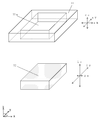
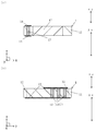
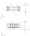
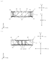
- FIG. 2A is a top view illustrating the electronic element mounting substrate according to the first embodiment
- FIG. 2B is a bottom view of FIG.
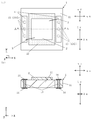
- FIG. 2 is an exploded perspective view of a first substrate and a second substrate of the electronic element mounting substrate shown in FIG. 1.
- FIG. 2 is a vertical cross-sectional view taken along line AA of the electronic element mounting substrate shown in FIG. 1A is a top view showing a state where an electronic element is mounted on the electronic element mounting substrate shown in FIG. 1A
- FIG. 2B is a longitudinal sectional view taken along line AA of FIG. is there.
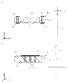
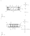
- (A) is a top view which shows the electronic element mounting substrate in 2nd Embodiment
- (b) is a bottom view of (a).
- FIG. 1 is a top view illustrating the electronic element mounting substrate according to the first embodiment
- FIG. 2B is a bottom view of FIG.
- FIG. 2 is an exploded perspective view of a first substrate and a second substrate of the electronic element mounting substrate shown in FIG.
- FIG. 5 is an exploded perspective view of a first substrate and a second substrate of the electronic element mounting substrate shown in FIG. 4.
- 5A is a vertical cross-sectional view taken along line AA of the electronic element mounting substrate shown in FIG. 5A
- FIG. 5B is an electronic element mounting substrate shown in FIG. 3 is a vertical sectional view taken along line BB of FIG. 5A
- FIG. 5B is a longitudinal sectional view taken along line AA in FIG. is there.
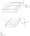
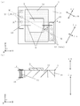
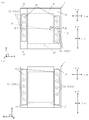
- (A) is a top view which shows the electronic element mounting substrate in 3rd Embodiment
- (b) is a bottom view of (a).
- FIG. 10 is an exploded perspective view of a first substrate and a second substrate of the electronic element mounting substrate shown in FIG. 9.
- 9A is a vertical cross-sectional view taken along line AA of the electronic element mounting substrate shown in FIG. 9A
- FIG. 9B is an electronic element mounting substrate shown in FIG. 9A.
- 3 is a vertical sectional view taken along line BB of FIG. 9A is a top view showing a state in which an electronic element is mounted on the electronic element mounting substrate shown in FIG. 9A
- FIG. 9B is a longitudinal sectional view taken along line AA in FIG. is there.
- (A) and (b) are top views showing another example of a state where an electronic element is mounted on the electronic element mounting substrate shown in FIG. 9 (a).
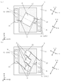
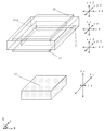
- FIG. 15 is an exploded perspective view of a first substrate, a third substrate, a fourth substrate, and a second substrate of the electronic element mounting substrate shown in FIG. 14A is a vertical cross-sectional view taken along line AA of the electronic element mounting substrate shown in FIG. 14A
- FIG. 14B is an electronic element mounting substrate shown in FIG. 14A.
- 3 is a vertical sectional view taken along line BB of FIG.
- (A) is a top view which shows the other example of the electronic element mounting board
- (b) is a bottom view of (a).
- FIG. 15 is an exploded perspective view of a first substrate, a third substrate, a fourth substrate, and a second substrate of the electronic element mounting substrate shown in FIG. 14A is a vertical cross-sectional view taken along line AA of the electronic element mounting substrate shown in FIG. 14A
- FIG. 14B is an electronic element mounting substrate shown in FIG. 14A.
- 3 is a vertical sectional view taken along line BB of
- FIG. 18 is an exploded perspective view of a first substrate, a third substrate, a fourth substrate, and a second substrate of the electronic element mounting substrate shown in FIG. 17A is a longitudinal sectional view taken along line AA of the electronic element mounting substrate shown in FIG. 17A
- FIG. 17B is an electronic element mounting substrate shown in FIG. 3 is a vertical sectional view taken along line BB of FIG.
- (A) is a top view which shows the other example of the electronic element mounting board
- (b) is a bottom view of (a).
- 20A is a vertical cross-sectional view taken along line AA of the electronic element mounting substrate shown in FIG. 20A
- FIG. 20B is an electronic element mounting substrate shown in FIG. 3 is a vertical sectional view taken along line BB of FIG.
- the electronic element mounting substrate 1 includes a first substrate 11 and a second substrate 12, as in the examples shown in FIGS.
- the electronic device includes, for example, a substrate 1 for an electronic element or the like, an electronic element 2 mounted on a mounting portion of the electronic element mounting substrate 1, and a wiring board on which the electronic element mounting substrate 1 is mounted.
- the electronic device is connected, for example, to a connection pad on a module substrate constituting the electronic module using a bonding material.
- the electronic element mounting substrate 1 includes a first substrate 11 having a first main surface and a second main surface opposite to the first main surface, and a first substrate 11 inside the first substrate 11 in plan view.
- a second substrate 12 that is located is made of a carbon material, and has a third main surface located on the first main surface side in the thickness direction and a fourth main surface located on the opposite side to the third main surface; It has a plurality of via conductors 13 located on the first substrate 11 with the second substrate 12 interposed therebetween.
- the second substrate 12 is formed by a plurality of via conductors 13 due to heat conduction in a direction (x direction in FIGS. 1 to 4) in which the plurality of via conductors 13 are located across the second substrate 12.
- the heat conduction is large in a direction perpendicular to the direction interposed between them (the y direction in FIGS. 1 to 4).
- the conductor layers 14 are provided on the first main surface and the second main surface of the first substrate 11, and are connected to both ends of the via conductor 13. 1 to 4, the electronic element 2 is mounted on an xy plane in a virtual xyz space.
- the upward direction refers to the positive direction of the virtual z-axis.
- the outer surface of the first substrate 11 and the inner surface of the through-hole 11 a which are invisible in a perspective view, are indicated by dotted lines in the first substrate 11.
- the second substrate 12 is shaded in the examples shown in FIGS. 1, 2, and 4A.
- a portion where the side surface of the via conductor 13 and the conductor layer 14 overlap with each other is indicated by a dotted line in plan view.
- the first substrate 11 has a first main surface (upper surface in FIGS. 1 to 4) and a second main surface (lower surface in FIGS. 1 to 4).
- the first main surface and the second main surface are located on opposite sides.
- the first substrate 11 is formed of a single layer or a plurality of insulating layers, and is a rectangular plate having two pairs of opposing sides (four sides) with respect to each of the first main surface and the second main surface in plan view. Shape.
- the first substrate 11 functions as a support for supporting the electronic element 2 and the second substrate 12.
- the first substrate 11 for example, ceramics such as an aluminum oxide sintered body (alumina ceramics), an aluminum nitride sintered body, a mullite sintered body, or a glass ceramic sintered body can be used.
- the first substrate 11 is, for example, an aluminum nitride sintered body
- the first substrate 11 is suitable for a raw material powder such as aluminum nitride (AlN), erbium oxide (Er 2 O 3 ), yttrium oxide (Y 2 O 3 ).
- An organic binder and a solvent are added and mixed to produce a slurry.
- the above-mentioned slurry is formed into a sheet by employing a conventionally known doctor blade method, calender roll method, or the like to produce a ceramic green sheet. If necessary, a plurality of ceramic green sheets are laminated and fired at a high temperature (about 1800 ° C.), whereby the first substrate 11 including a single layer or a plurality of insulating layers is manufactured.
- the second substrate 12 has a third main surface (upper surface in FIGS. 1 to 4) and a fourth main surface (lower surface in FIGS. 1 to 4) located on the first main surface side of the first substrate 11. I have.
- the third main surface and the fourth main surface are located on opposite sides of each other.
- the second substrate 12 is located inside the first substrate 11, as in the examples shown in FIGS.
- the second substrate 12 has a mounting portion for mounting the electronic element 2 on the third main surface, and functions as a support for supporting the electronic element 2.
- the second substrate 12 is made of, for example, a carbon material, and is formed as a structure in which graphene in which six-membered rings are connected by a covalent bond is laminated. Each surface is made of a material joined by van der Waals force.
- the via conductor 13 is provided in the thickness direction of the first substrate 11.
- the via conductor 13 is provided so as to penetrate the first main surface and the second main surface of the first substrate 11 in the examples shown in FIGS.
- the conductor layers 14 are provided on the first main surface and the second main surface of the first substrate 11, and are connected to both ends of the via conductor 13.
- the plurality of via conductors 13 are located on the first substrate 11 with the second substrate 12 interposed therebetween in plan view.
- the direction in which the plurality of via conductors 13 are located with the second substrate 12 interposed therebetween is the x direction in the examples shown in FIGS.
- the via conductor 13 and the conductor layer 14 are for electrically connecting, for example, the electronic element 2 and a wiring conductor of a wiring board.
- the conductor layer 14 is used as a connection portion of the connection member 3 such as a bonding wire and a connection portion with a wiring conductor of a wiring board.
- the via conductor 13 and the conductor layer 14 generate heat when a current is applied to operate the electronic element 2.
- the via conductor 13 and the conductor layer 14 are, for example, metal powder metalized mainly containing tungsten (W), molybdenum (Mo), manganese (Mn), silver (Ag) or copper (Cu).
- W tungsten
- Mo molybdenum
- Mn manganese
- Ag silver
- Cu copper
- the first substrate 11 is made of an aluminum nitride sintered body
- a metallized paste obtained by adding a suitable organic binder and a solvent to a high melting point metal powder such as W, Mo or Mn is mixed.
- the ceramic green sheet for the first substrate 11 is formed by printing and applying a predetermined pattern in advance by a screen printing method and firing the ceramic green sheet for the first substrate 11 at the same time.
- the via conductor 13 is formed, for example, by forming a through-hole of a through conductor in a ceramic green sheet for the first substrate 11 by a processing method such as punching by a mold or punching or laser processing.
- the metallized paste is printed and applied by a printing means such as a screen printing method, filled, and fired together with the ceramic green sheet for the first substrate 11.
- the conductor layer 14 is formed, for example, by printing and applying a metallized paste for the conductor layer 14 to a predetermined region of the surface of the ceramic green sheet for the first substrate 11 by the above-described printing means, and firing the paste together with the ceramic green sheet for the first substrate 11. It is formed by doing.
- the metallized paste is prepared by adding an appropriate solvent and binder to the above-mentioned metal powder and kneading the mixture to adjust the viscosity to an appropriate level.
- glass powder and ceramic powder may be included.
- a metal plating layer is applied to the surface of the conductor layer 14 exposed from the first substrate 11 by an electroplating method or an electroless plating method.
- the metal plating layer is made of a metal such as nickel, copper, gold or silver which has excellent corrosion resistance and connection member connection properties.
- a nickel plating layer having a thickness of about 0.5 to 5 ⁇ m and a gold plating layer having a thickness of about 0.1 to 3 ⁇ m are provided. Are sequentially applied. With the metal plating layer, corrosion of the conductor layer 14 can be effectively suppressed, and the conductor layer 14 is connected to the connection member 3 such as a bonding wire, and the conductor layer 14 is connected to the connection member 3 formed on the module substrate. Bonding with the connection pad 41 can be strengthened.
- the metal plating layer is not limited to the nickel plating layer / gold plating layer, but may be another metal plating layer including a nickel plating layer / palladium plating layer / gold plating layer.
- the first substrate 11 is preferably made of an aluminum nitride sintered body having excellent thermal conductivity.
- the first substrate 11 and the second substrate 12 are bonded to each other by bonding the inner surface of the through hole 11a of the first substrate 11 and the outer surface of the second substrate 12 with an active brazing material such as a TiCuAg alloy or TiSnAgCu. You.
- the bonding material is disposed between the first substrate 11 and the second substrate 12 with a thickness of about 10 ⁇ m.
- the first substrate 11 has a square shape in a plan view, and has a square through hole 11a penetrating the first main surface and the second main surface in a plan view.
- the first substrate 11 may have a frame shape.
- the second substrate 12 has a square shape in plan view.
- the square shape is a square shape such as a square shape and a rectangular shape.
- the first substrate 11 and the second substrate 12 are square in plan view, and a square composite substrate is formed.
- the substrate thickness T1 of the first substrate 11 is, for example, about 100 ⁇ m to 2000 ⁇ m
- the substrate thickness T2 of the second substrate 12 is, for example, about 100 ⁇ m to 2000 ⁇ m.
- the thickness T1 of the first substrate 11 and the thickness T2 of the second substrate 12 are formed to be substantially the same (0.9T1 ⁇ T2 ⁇ 1.1T1).
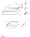
- the thermal conductivity ⁇ of the first substrate 11 is substantially constant in the x direction and the y direction in the plane direction, and the z direction in the thickness direction of the first substrate 11 is also constant in the plane direction.
- Direction and the y direction ( ⁇ x ⁇ ⁇ y ⁇ ⁇ z).
- a substrate having a thermal conductivity ⁇ of about 100 to 200 W / m ⁇ K is used as the first substrate 11.
- the thermal conductivity ⁇ of the second substrate 12 differs in magnitude between the x direction and the y direction in the plane direction.
- the thermal conductivity ⁇ of the second substrate 12 the y direction in the plane direction and the z direction in the thickness direction are equivalent, and the x direction in the plane direction is different.
- the relationship between the thermal conductivity ⁇ x, ⁇ y, and ⁇ z in each direction of the second substrate 12 shown in FIG. 2 is “thermal conductivity ⁇ y ⁇ thermal conductivity ⁇ z >> thermal conductivity ⁇ x”.
- the thermal conductivity ⁇ y and the thermal conductivity ⁇ z of the second substrate 12 are about 1000 W / m ⁇ K, and the thermal conductivity ⁇ x of the second substrate 12 is about 4 W / m ⁇ K.
- some of the thermal conductivity ⁇ x, ⁇ y, ⁇ z, ⁇ x, ⁇ y, ⁇ z are omitted.
- the electronic device can be manufactured by mounting the electronic element 2 on the mounting portion of the second substrate 12 of the electronic element mounting substrate 1.
- the electronic element 2 is located on the mounting portion of the second substrate 12 so as to be sandwiched between the via conductors 13 as in the example shown in FIG.
- the electronic device may be manufactured by mounting the electronic element mounting substrate 1 on which the electronic element 2 is mounted on a wiring board or an electronic element mounting package.
- the electronic element 2 mounted on the electronic element mounting substrate 1 is, for example, a light emitting element such as an LD (Laser Diode) or an LED (Light Emitting Diode) or a light receiving element such as a PD (Photo Diode).
- the electrode of the electronic element 2 and the conductor layer 14 are connected via the connection member 3 such as a bonding wire.
- the connection member 3 such as a bonding wire.
- the wiring substrate or the electronic element mounting package uses, for example, an insulating base made of ceramics or the like, like the first substrate 11. And has a wiring conductor on the surface.
- the conductor layer 14 of the electronic element mounting board 1 and the wiring conductor of the wiring board or the electronic element mounting package are electrically connected. Connected to.
- the first substrate 11 having the first main surface and the second main surface opposite to the first main surface, and the first substrate 11 in plan view.
- a second substrate 12 which is located inside, is made of a carbon material, has a third main surface located on the first main surface side in the thickness direction, and has a fourth main surface located on the opposite side to the third main surface;
- the heat conduction in the direction perpendicular to the direction in which the plurality of via conductors 13 are located with the second substrate 12 interposed therebetween is greater than the heat conduction in the direction located at.
- the via conductor 13 when the via conductor 13 generates heat during operation of the electronic device, the heat transmitted from the via conductor 13 to the second substrate 12 is applied to the second substrate 12 over the entire thickness (z direction) of the via conductor 13. From the outer edge, a plurality of via conductors 13 are transmitted along the outer edge of the first substrate 11 in a direction perpendicular to the direction positioned across the second substrate 12, and heat transfer from the via conductor 13 to the electronic element 2 is performed. Is suppressed, the heat of the via conductor 13 is satisfactorily radiated, and a decrease in the output of the electronic element 2 can be suppressed.
- a decrease in output of the light emitting element can be suppressed, and an electronic element mounting substrate capable of emitting light from the light emitting element satisfactorily can be obtained.
- the heat of the electronic element 2 is transmitted in a direction perpendicular to the direction in which the plurality of via conductors 13 of the second substrate 12 are positioned across the second substrate 12 and in the thickness direction of the second substrate 12. 2 can be satisfactorily radiated, and a decrease in the output of the electronic element 2 can be suppressed.
- the electronic device mounting substrate 1 having the above configuration and the electronic device 2 mounted on the mounting portion of the electronic device mounting substrate 1 have long-term reliability. An excellent electronic device can be obtained.
- the electronic device of the present embodiment is connected to the conductor layer of the electronic element mounting substrate 1 and the connection pad of the module substrate via a bonding material such as solder, thereby forming an electronic module, and connecting the electronic element 2 and the module substrate.
- the pads are electrically connected.
- the electronic device When the electronic device has a wiring board or an electronic element storage package on which the electronic element mounting board 1 is mounted, the wiring conductors of the wiring board or the electronic element storage package and the connection pads of the module substrate are provided. It is connected via a bonding material such as solder to form an electronic module. As described above, the electronic element 2 is electrically connected to the connection pads of the module substrate.
- the electronic device having the above configuration and the module substrate to which the electronic device is connected have excellent long-term reliability.
- the second substrate 12 has a thickness direction more than a direction perpendicular to the thickness direction.
- the heat conduction of the via conductor 13 is large ( ⁇ z >> ⁇ x)
- the heat of the via conductor 13 transmitted to the second substrate 12 is difficult to stay inside the second substrate 12, and the thickness of the via conductor 13 (z direction)
- a plurality of via conductors 13 are transmitted from the outer edge of the second substrate 12 along the outer edge of the first substrate 11 in a direction perpendicular to the direction in which the second substrate 12 is interposed.
- the heat transfer from 13 to the electronic element 2 is suppressed, the heat of the via conductor 13 is radiated well, and the output of the electronic element 2 can be prevented from lowering.
- the via conductor 13 provided inside the first substrate 11 and the conductor layer 14 provided on the first main surface and the second main surface of the first substrate 11 are formed by the cofire method in the above-described example.
- the conductor 13 and the conductor layer 14 may be formed by a conventionally known thin film method and plating method.
- the conductor layer 14 provided on the first main surface or the second main surface of the first substrate 11 may be a conductor layer 14 using a conventionally known post-fire method or the like.
- the via conductor 13 and the conductor layer 14 are formed by a thin film layer and a plating method, the first substrate 11 and the second substrate 12 are joined with a joining material to produce a composite substrate.
- the electronic element mounting substrate 1 is favorably formed.
- the electronic element mounting substrate 1 according to the second embodiment is different from the electronic element mounting substrate 1 according to the above-described embodiment in that, in plan view, the plurality of via conductors 13 allow the second substrate 12 to have high heat conduction. This is a point that continues in the direction (the y direction in FIGS. 5 to 8). In FIG. 7B, the outer edge of the second substrate 12 is indicated by a dotted line for the sake of convenience in order to show the positional relationship between the first substrate 11 and the second substrate 12.
- a via conductor group 13G is formed by connecting at least two or more via conductors 13 in a direction in which the heat conduction of the second substrate 12 is large in a plan view. .
- three via conductors 13 are respectively connected in a direction in which the heat conduction of the second substrate 12 is large, and are located on the first substrate 11 with the second substrate 12 interposed therebetween.
- a plurality of via conductor groups 13G in the electronic element mounting substrate 1 according to the second embodiment, the second substrate 12 has a direction in which a plurality of via conductor groups 13G are located across the second substrate 12 in a plan view (x direction in FIGS. 5 to 8).
- the heat conduction in the direction perpendicular to the direction in which the plurality of via conductor groups 13G interpose the second substrate 12 is larger than the heat conduction ( ⁇ y ⁇ ⁇ z >>). ⁇ x).
- the electronic element 2 is located on the mounting portion of the second substrate 12 so as to be sandwiched by a via conductor group 13G including a plurality of via conductors 13, as in the example shown in FIG.
- the outer surface of the first substrate 11 and the inner surface of the through hole 11a, which are invisible in a perspective view, are indicated by dotted lines in the example shown in FIG.
- the second substrate 12 is shaded in the examples shown in FIGS. 5, 6, and 8A.
- a portion where the side surface of the via conductor 13 and the conductor layer 14 overlap with each other is indicated by a dotted line in plan view.
- the heat transmitted from the via conductor 13 to the second substrate 12 is equal to the thickness of the via conductor 13.
- a plurality of via conductors 13 located along the outer edge of the first substrate 11 are transmitted from the outer edge of the second substrate 12 in a direction perpendicular to the direction in which the second substrate 12 is sandwiched.
- a decrease in output of the light emitting element can be suppressed, and an electronic element mounting substrate capable of emitting light from the light emitting element satisfactorily can be obtained.
- the heat of the electronic element 2 is transmitted to the second substrate 12 in a direction perpendicular to the direction in which the plurality of via conductors 13 are positioned across the second substrate 12 and in a thickness direction of the second substrate 12.
- the heat of the element 2 can be satisfactorily radiated, and a decrease in the output of the electronic element 2 can be suppressed.
- the plurality of via conductors 13 are continuous in the direction in which the thermal conductivity of the second substrate 12 is large in plan view, and each via conductor in the plurality of via conductors 13 is formed.
- the heat of the conductor 13 hardly stays on the first substrate 11, and the heat of the via conductor 13 transmitted to the second substrate 12 increases from the outer edge of the second substrate 12 over the entire thickness (z direction) of the via conductor 13.
- the plurality of via conductors 13 located along the outer edge of the first substrate 11 are transmitted in a direction perpendicular to the direction located across the second substrate 12, so that heat transfer from the via conductor 13 to the electronic element 2 is suppressed.
- the heat of the via conductor 13 can be satisfactorily radiated, and the output of the electronic element 2 can be effectively prevented from lowering.
- the first substrate 11 has a square shape in a plan view, and has a square through hole 11a penetrating the first main surface and the second main surface in a plan view.
- the first substrate 11 may have a frame shape.
- the second substrate 12 has a square shape in plan view.
- the square shape is a square shape such as a square shape and a rectangular shape.
- the first substrate 11 and the second substrate 12 are square in plan view, and a square composite substrate is formed.
- the plurality of via conductors 13 located in the same direction are transmitted equally in a direction perpendicular to the direction located across the second substrate 12, heat transfer from the via conductor 13 to the electronic element 2 is suppressed, and Heat can be satisfactorily radiated, and a decrease in the output of the electronic element 2 can be effectively suppressed.
- the second substrate 12 has a rectangular shape in plan view and the plurality of via conductors 13 (via conductor group 13G) are connected along opposing sides of the second substrate 12, the plurality of via conductors 13
- the heat of each via conductor 13 in the (via conductor group 13G) is easily transmitted to the second substrate 12 equally, and the heat of the via conductor group 13 transmitted to the second substrate 12 is reduced by the thickness of the via conductor 13 (z direction).
- a plurality of via conductors 13 located along the outer edge of the first substrate 11 are transmitted from the outer edge of the second substrate 12 in a direction perpendicular to the direction located across the second substrate 12,
- the heat transfer from the via conductor 13 to the electronic element 2 is suppressed, the heat of the via conductor 13 is satisfactorily radiated, and the decrease in the output of the electronic element 2 can be effectively suppressed.
- both ends of the second substrate 12 in the direction in which the heat conduction of the second substrate 12 is large are, as in the example shown in FIG.
- the via conductor 13 is located outside the via conductor 13 located at the end, the heat transmitted from the via conductor 13 to the second substrate 12 is transferred to the second substrate 12 in the direction in which the heat conduction of the second substrate 12 is large.
- the heat transfer from the end to the electronic element 2 is suppressed, and a decrease in the output of the electronic element 2 can be suppressed.
- the first substrate 11 is perpendicular to the direction in which the plurality of via conductors 13 located along the outer edge of the first substrate 11 sandwich the second substrate 12.
- the auxiliary layer 15 is connected to the wiring conductor of the wiring board or the package for housing the electronic element, or to the connection pad of the module substrate, and the heat transmitted to the first substrate 11 is connected. Is transferred to the wiring board, the package for accommodating the electronic element, or the substrate for the module, thereby radiating the heat satisfactorily and effectively preventing the output of the electronic element 2 from being reduced.
- the electronic element mounting substrate 1 of the second embodiment can be manufactured using the same manufacturing method as the electronic element mounting substrate 1 of the above-described embodiment.
- the electronic device mounting board 1 according to the third embodiment is different from the electronic element mounting board 1 according to the above-described embodiment in that the opposing sides of the second substrate 12 and the plurality of via conductors 13 are different from each other. Is a point that intersects obliquely with the direction located across the. In FIG. 11B, the outer edge of the second substrate 12 is indicated by a dotted line for convenience to show the positional relationship between the first substrate 11 and the second substrate 12.
- the electronic element mounting substrate 1 according to the third embodiment forms a via conductor group 13G by connecting two or more via conductors 13 in a plan view. Has formed. 9 to 12, in plan view, three via conductors 13 are continuous, and have two via conductor groups 13G located on the first substrate 11 with the second substrate 12 interposed therebetween.
- the opposite side of the second substrate 12 obliquely intersects with the direction in which the plurality of via conductors 13 are located across the second substrate 12 means that the opposite side is located on the first substrate 11 across the second substrate 12. This indicates that the virtual straight line NN passing through the via conductor 13 and the opposite side of the second substrate 12 obliquely intersect.
- the two via conductor groups 13G located on the first substrate 11 with the second substrate 12 interposed therebetween include the first substrate 11, the second substrate 12, and the electronic element as shown in the examples shown in FIGS. They are arranged symmetrically with respect to the center of the mounting substrate 1.
- the via conductor 13 is a via conductor group 13G
- a virtual straight line NN passing through the center of the via conductor group 13G located on the first substrate 11 with the second substrate 12 interposed therebetween, and an opposite side of the second substrate 12 Indicate that they intersect at an angle.
- the plurality of via conductor groups 13G are located across the second substrate 12 due to heat conduction in the direction in which the plurality of via conductor groups 13G are located across the second substrate 12.
- the heat conduction in the direction perpendicular to the direction is larger ( ⁇ y ⁇ ⁇ z >> ⁇ x). That is, from the direction of a virtual straight line passing through the via conductor 13 (the center of the via conductor group 13G) located on the first substrate 11 with the second substrate 12 interposed therebetween, the via conductor 13 (via conductor group 13G) located on the first substrate 11 is viewed. (Center of the center line), the heat conduction in the direction perpendicular to the direction of the imaginary straight line passing through the center line is large ( ⁇ yz ⁇ z >> ⁇ x).
- the outer surface of the first substrate 11 and the inner surface of the through hole 11 a which are invisible in a perspective view, are indicated by dotted lines in the first substrate 11.
- the second substrate 12 is shaded in the examples shown in FIGS. 9, 10, and 12A.
- a portion where the side surface of the via conductor 13 and the conductor layer 14 overlap in a plan view is indicated by a dotted line.
- the heat transmitted from the via conductor 13 to the second substrate 12 is equal to the thickness of the via conductor 13.
- a plurality of via conductors 13 located along the outer edge of the first substrate 11 are transmitted from the outer edge of the second substrate 12 in a direction perpendicular to the direction in which the second substrate 12 is sandwiched.
- the heat transmitted to the second substrate 12 is transmitted well in a direction perpendicular to a direction of a virtual straight line passing through the via conductor 13 (the center of the via conductor group 13G) located on the first substrate 11, so that the via conductor group 13G, the heat of the adjacent via conductor 13 is transferred well, the heat transfer from the via conductor 13 to the electronic element 2 is suppressed, the heat of the via conductor 13 is radiated well, and the output of the electronic element 2 is reduced. Can be suppressed.
- a decrease in output of the light emitting element can be suppressed, and an electronic element mounting substrate capable of emitting light from the light emitting element satisfactorily can be obtained.
- the first substrate 11 has a square shape in a plan view, and has a square through hole 11a penetrating the first main surface and the second main surface in a plan view.
- the first substrate 11 may have a frame shape.
- the second substrate 12 has a square shape in plan view.
- the square shape is a square shape such as a square shape and a rectangular shape.
- the first substrate 11 and the second substrate 12 are square in plan view, and a square composite substrate is formed.
- the angle ⁇ between a virtual straight line passing through the via conductor 13 (the center of the via conductor group 13G) located on the first substrate 11 with the second substrate 12 interposed therebetween and the side of the second substrate 12 is 10 to 80 degrees. There may be.
- the outer side of the electronic element 2 is aligned with the direction of a virtual straight line NN passing through the via conductor 13 (the center of the via conductor group 13G) located on the first substrate 11.
- the heat transmitted from the plurality of via conductors 13 to the second substrate 12 is separated from the electronic element 2 and easily transmitted, so that the heat transfer from the via conductor 13 to the electronic element 2 is suppressed, The heat of the conductor 13 can be satisfactorily radiated and the output of the electronic element 2 can be prevented from lowering.
- each of the electronic elements 2 moves in the direction of a virtual straight line NN passing through the via conductors 13 (centers of the via conductor group 13G) located on the first substrate 11.
- the via conductors 13 centers of the via conductor group 13G located on the first substrate 11.
- a light-emitting element is used as the electronic element 2
- the electronic element mounting substrate 1 of the third embodiment can be manufactured using the same manufacturing method as the electronic element mounting substrate 1 of the above-described embodiment.
- the electronic device mounting substrate 1 of the fourth embodiment differs from the electronic device mounting substrate 1 of the above-described embodiment in that the third main surface or the fourth main surface of the second substrate 12 is provided with another substrate ( It has a third substrate 16 and a fourth substrate 17).
- the outer edge of the second substrate 12 is indicated by a dotted line for convenience to show the positional relationship between the first substrate 11 and the second substrate 12.
- a region of the main surface (the upper surface in FIGS. 14 to 16) of the third substrate 16 that overlaps the second substrate 12 is used as a mounting portion for the electronic device 2.
- the outer surface of the first substrate 11 and the inner surface of the through hole 11a, which are invisible in a perspective view, are indicated by dotted lines.
- the second substrate 12 is shaded in the example shown in FIG.
- the portions where the side surface of the second substrate 12, the side surface of the via conductor 13, and the conductor layer 14 overlap each other are shown by dotted lines in plan perspective.
- the heat transmitted from the via conductor 13 to the second substrate 12 is equal to the thickness of the via conductor 13.
- a plurality of via conductors 13 located along the outer edge of the first substrate 11 are transmitted from the outer edge of the second substrate 12 in a direction perpendicular to the direction in which the second substrate 12 is sandwiched.
- the conductor layer 14 is formed large on the main surface (the lower surface in FIGS. 14 to 16) of the fourth substrate 17 as in the examples shown in FIGS. 14 to 16, the wiring of the wiring board or the package for housing the electronic element is formed.
- the connection with the conductor or the connection pad of the module substrate can be made good, and the heat of the electronic element 2 can be satisfactorily transferred to the wiring board, the package for housing the electronic element, or the module substrate.
- a decrease in output of the light emitting element can be suppressed, and an electronic element mounting substrate capable of emitting light from the light emitting element satisfactorily can be obtained.
- the first substrate 11 has a rectangular shape in plan view, and has a rectangular through hole 11 penetrating the first main surface and the second main surface in plan perspective. Note that the first substrate 11 may have a frame shape.
- the second substrate 12 has a square shape in plan view.
- the third substrate 16 has a square shape in plan view.
- the fourth substrate 17 has a square shape in plan view.
- the inner surface of the through hole 11a of the first substrate 11 is bonded to the side surface of the second substrate 12, and the third main surface of the second substrate 12 and the third substrate 16, and the fourth main surface of the second substrate 12 and the fourth substrate By bonding the composite substrate 17 with the substrate 17, a square composite substrate is formed.
- first main surface of the first substrate 11 may be bonded to the third substrate 16, and the second main surface of the first substrate 11 may be bonded to the fourth substrate 17.
- the square shape is a square shape such as a square shape and a rectangular shape.
- the first substrate 11 and the second substrate 12 are square in plan view, and a square composite substrate is formed.
- the third substrate 16 and the fourth substrate 17 can be manufactured by the same material and method as the first substrate 11 described above.
- the thermal conductivity ⁇ 2 of the third substrate 16 and the fourth substrate 17 is substantially constant in the x direction and the y direction in the plane direction, and also in the z direction in the thickness direction of the fourth substrate 14. It is equivalent to the x direction and the y direction in the plane direction ( ⁇ x2 ⁇ ⁇ y2 ⁇ ⁇ z2).
- a substrate having a thermal conductivity ⁇ 2 of about 100 to 200 W / m ⁇ K is used as the first substrate 16.
- the first substrate 11 and the second substrate 12 are located between the third substrate 16 and the fourth substrate 17, the mounting of electronic elements due to the difference in thermal expansion between the first substrate 11 and the second substrate 12 Distortion of the electronic substrate 1 is suppressed, and displacement of the electronic element 2 or distortion of the electronic element mounting substrate 1 is suppressed, so that light can be easily emitted favorably.
- the third substrate 16 and the fourth substrate 17 use an insulator of substantially the same material as the first substrate 11, that is, for example, as the first substrate 11, a 150 W / m ⁇ K aluminum nitride material is used.
- a 150 W / m ⁇ K aluminum nitride material is used as the third substrate 16 and the fourth substrate 17, the distortion of the electronic element mounting substrate 1 is more effectively achieved. , It is possible to favorably emit light.
- the thickness T3 of the third substrate 16 is, for example, about 50 ⁇ m to 500 ⁇ m.
- the thickness T4 of the fourth substrate 17 is, for example, about 50 ⁇ m to 500 ⁇ m.
- the electronic element can be more effectively used.
- the thickness of the third substrate T3 is 100 ⁇ m
- the thickness of the fourth substrate 17 may be 100 ⁇ m (90 ⁇ m to 110 ⁇ m).
- the thickness T3 of the third substrate 16 is smaller than the thickness T1 of the first substrate 11 and the thickness T2 of the second substrate 12, and the thickness T4 of the fourth substrate 17 is the thickness T1 of the first substrate 11 and the second substrate 12.
- the thickness is smaller than the thickness T2 of the substrate 12
- the heat of the electronic element 2 can be satisfactorily transferred to the wiring board, the package for accommodating the electronic element, or the module substrate. By suppressing the distortion, it is possible to favorably emit light.
- the first substrate 11 has a square frame shape
- the second substrate 12, the third substrate 16, and the fourth substrate 17 have a rectangular shape.
- a rectangular composite substrate is formed.
- the third substrate 16 and the fourth substrate 17 are also provided with the via conductor 13 and the conductor layer.
- the via conductor 13 and the conductor layer 14 may be formed by a conventionally known thin film method and plating method.
- a through-hole serving as the via conductor 13 may be formed in the composite substrate, and the via conductor 13 and the conductor layer 14 may be formed.
- the third substrate 16 or the fourth substrate 17 is, as shown in FIGS. 17 to 19, a third main surface and a fourth main surface of the second substrate 12 and a first main surface of the first substrate 11.
- the inner surface of the first substrate 11 may be disposed so as to cover the inner edge of the first substrate 11 and the inner surface of the second substrate, as shown in FIGS. 12, the fourth substrate 17 covers the second main surface of the first substrate 11 and the fourth main surface of the second substrate 12, and the conductor layer 14 provided on the first substrate 11 is exposed. It is also possible to adopt a configuration in which a through portion is provided on the third substrate 16 and the fourth substrate 17.
- the electronic element mounting substrate 1 of the fourth embodiment can be manufactured using the same manufacturing method as the electronic element mounting substrate 1 of the above-described embodiment.
- the present disclosure is not limited to the above-described embodiments, and various modifications are possible.
- the composite substrate has a square shape having a notch or a chamfer at a corner of the composite substrate. No problem.
- the third substrate 16 is disposed on the third main surface of the second substrate 12.
- the fourth substrate 17 may be arranged on the fourth main surface of the second substrate 12.
- the electronic element mounting substrate 1 may be a combination of the element mounting substrates 1 of the first to fourth embodiments.
- the opposite side of the second substrate 12 and the plurality of via conductors 13 The direction located across the substrate 12 may intersect obliquely.
Landscapes
- Engineering & Computer Science (AREA)
- Chemical & Material Sciences (AREA)
- Ceramic Engineering (AREA)
- Inorganic Chemistry (AREA)
- Microelectronics & Electronic Packaging (AREA)
- Structure Of Printed Boards (AREA)
- Cooling Or The Like Of Semiconductors Or Solid State Devices (AREA)
- Led Device Packages (AREA)
- Semiconductor Lasers (AREA)
- Production Of Multi-Layered Print Wiring Board (AREA)
Abstract
Description
本発明は、電子素子搭載用基板、電子装置および電子モジュールに関するものである。 The present invention relates to an electronic element mounting substrate, an electronic device, and an electronic module.
従来、電子素子搭載用基板は、第1主面と第2主面と側面とを有する絶縁基板と、絶縁基板の第1主面に位置した電子素子の搭載部および配線層とを有している。電子素子搭載用基板において、電子素子の搭載部に電子素子を搭載した後、電子素子収納用パッケージに搭載されて電子装置となる(特開2013-175508号公報参照。)。 2. Description of the Related Art Conventionally, an electronic element mounting substrate includes an insulating substrate having a first main surface, a second main surface, and side surfaces, an electronic element mounting portion and a wiring layer located on the first main surface of the insulating substrate. I have. In the electronic element mounting substrate, the electronic element is mounted on a mounting portion of the electronic element, and then mounted on an electronic element housing package to form an electronic device (see Japanese Patent Application Laid-Open No. 2013-175508).
本開示の電子素子搭載用基板は、第1主面および該第1主面と反対側に位置する第2主面を有した第1基板と、平面視で該第1基板の内側に位置し、炭素材料からなり、厚み方向における前記第1主面側に位置した第3主面および該第3主面と反対側に位置する第4主面を有する第2基板と、平面視において、該第2基板を挟んで前記第1基板に位置した複数のビア導体とを有しており、平面視において、前記第2基板は、前記複数のビア導体が前記第2基板を挟んで位置した方向の熱伝導より前記複数のビア導体が前記第2基板を挟んで位置した方向に垂直に交わる方向の熱伝導が大きい。 An electronic element mounting substrate according to an embodiment of the present disclosure includes a first substrate having a first main surface and a second main surface located on a side opposite to the first main surface, and a first substrate located inside the first substrate in plan view. A second substrate made of a carbon material and having a third main surface located on the first main surface side in a thickness direction and a fourth main surface located on the opposite side to the third main surface; And a plurality of via conductors located on the first substrate with the second substrate interposed therebetween, and in a plan view, the second substrate has a direction in which the plurality of via conductors are located with the second substrate interposed therebetween. The heat conduction in the direction perpendicular to the direction in which the plurality of via conductors are located with the second substrate interposed therebetween is greater than the heat conduction.
本開示の電子装置は、上記構成の電子素子搭載用基板と、該電子素子搭載用基板の前記搭載部に搭載された電子素子と、前記電子素子搭載用基板が搭載された配線基板または電子素子収納用パッケージとを有している。 An electronic device according to an embodiment of the present disclosure includes an electronic element mounting substrate configured as described above, an electronic element mounted on the mounting portion of the electronic element mounting substrate, and a wiring board or an electronic element mounted with the electronic element mounting substrate. And a storage package.
本開示の電子モジュールは、上記構成の電子装置と、該電子装置が接続されたモジュール用基板とを有する。 電子 The electronic module according to the present disclosure includes the electronic device having the above configuration, and a module substrate to which the electronic device is connected.
本開示のいくつかの例示的な実施形態について、添付の図面を参照しつつ説明する。 Some exemplary embodiments of the present disclosure will be described with reference to the accompanying drawings.
(第1の実施形態)
本開示の第1の実施形態における電子素子搭載用基板1は、図1~図4に示された例のように、第1基板11と第2基板12とを含んでいる。電子装置は、例えば、電子素子等用基板1と、電子素子搭載用基板1の搭載部に搭載された電子素子2と、電子素子搭載用基板1が搭載された配線基板とを含んでいる。電子装置は、例えば、電子モジュールを構成するモジュール用基板上の接続パッドに接合材を用いて接続される。
(1st Embodiment)
The electronic
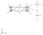
本実施形態における電子素子搭載用基板1は、第1主面および第1主面と反対側に位置する第2主面を有した第1基板11と、平面視で第1基板11の内側に位置し、炭素材料からなり、厚み方向における第1主面側に位置した第3主面および第3主面と反対側に位置する第4主面を有する第2基板12と、平面視において、第2基板12を挟んで第1基板11に位置した複数のビア導体13とを有している。平面視において、第2基板12は、複数のビア導体13が第2基板12を挟んで位置した方向(図1~図4ではx方向)の熱伝導より複数のビア導体13が第2基板12を挟んで位置した方向に垂直に交わる方向(図1~図4ではy方向)の熱伝導が大きい。導体層14は、第1基板11の第1主面および第2主面に設けられており、ビア導体13の両端部に接続している。図1~図4において、電子素子2は仮想のxyz空間におけるxy平面に実装されている。図1~図4において、上方向とは、仮想のz軸の正方向のことをいう。なお、以下の説明における上下の区別は便宜的なものであり、実際に電子素子搭載用基板1等が使用される際の上下を限定するものではない。
The electronic
第1基板11は、図2に示す例において、斜視にて不可視となる第1基板11の外面および貫通穴11aの内面とを点線にて示している。第2基板12は、図1、図2、図4(a)に示す例において、網掛けにて示している。図1および図4(a)に示す例において、平面視において、ビア導体13の側面と導体層14とが重なる部分を点線にて示している。
In the example shown in FIG. 2, the outer surface of the
第1基板11は、第1主面(図1~図4では上面)および第2主面(図1~図4では下面)を有している。第1主面と第2主面とは互いに反対側に位置している。第1基板11は、単層または複数の絶縁層からなり、平面視において、第1主面および第2主面のそれぞれに対して二組の対向する辺(4辺)を有した方形の板状の形状を有している。第1基板11は、電子素子2および第2基板12を支持するための支持体として機能される。
The
第1基板11は、例えば、酸化アルミニウム質焼結体(アルミナセラミックス),窒化アルミニウム質焼結体,ムライト質焼結体またはガラスセラミックス焼結体等のセラミックスを用いることができる。第1基板11は、例えば窒化アルミニウム質焼結体である場合であれば、窒化アルミニウム(AlN),酸化エルビニウム(Er2O3)、酸化イットリウム(Y2O3)等の原料粉末に適当な有機バインダーおよび溶剤等を添加混合して泥漿物を作製する。上記の泥漿物を、従来周知のドクターブレード法またはカレンダーロール法等を採用してシート状に成形することによってセラミックグリーンシートを作製する。必要に応じて、セラミックグリーンシートを複数枚積層し、高温(約1800℃)で焼成することによって、単層または複数の絶縁層からなる第1基板11が製作される。
For the
第2基板12は、第1基板11の第1主面側に位置した第3主面(図1~図4では上面)および第4主面(図1~図4では下面)を有している。第3主面と第4主面とは互いに反対側に位置している。第2基板12は、図1~図4に示される例のように、第1基板11の内側に位置している。第2基板12は、第3主面に電子素子2を搭載する搭載部を有しており、電子素子2を支持するための支持体として機能される。
The
第2基板12は、例えば、炭素材料からなり、六員環が共有結合でつながったグラフェンが積層した構造体として形成される。各面がファンデルワールス力で結合された材料である。
The
ビア導体13は、第1基板11の厚み方向に設けられている。ビア導体13は、図1~図4に示す例において、第1基板11の第1主面と第2主面とを貫通して設けている。導体層14は、第1基板11の第1主面および第2主面に設けられており、ビア導体13の両端部に接続している。
The via
また、複数のビア導体13は、平面視において、第2基板12を挟んで第1基板11に位置している。複数のビア導体13が第2基板12を挟んで位置した方向とは、図1~図4に示す例において、x方向である。
The plurality of via
ビア導体13および導体層14は、例えば、電子素子2と配線基板の配線導体とを電気的に接続するためのものである。また、導体層14は、ボンディングワイヤ等の接続部材3の接続部、配線基板の配線導体との接続部として用いられる。ビア導体13および導体層14は、電子素子2を作動させるために電流を印加した際に発熱する。
The via
ビア導体13および導体層14は、例えばタングステン(W),モリブデン(Mo),マンガン(Mn),銀(Ag)または銅(Cu)等を主成分とする金属粉末メタライズである。例えば、第1基板11が窒化アルミニウム質焼結体から成る場合であれば、W,MoまたはMn等の高融点金属粉末に適当な有機バインダーおよび溶媒等を添加混合して得たメタライズペーストを、第1基板11用のセラミックグリーンシートに予めスクリーン印刷法によって所定のパターンに印刷塗布して、第1基板11用のセラミックグリーンシートと同時に焼成することによって、形成される。ビア導体13は、例えば、第1基板11用のセラミックグリーンシートに金型またはパンチングによる打ち抜き加工またはレーザー加工等の加工方法によって貫通導体の貫通孔を形成し、上記の貫通孔にビア導体13用のメタライズペーストをスクリーン印刷法等の印刷手段によって印刷塗布して充填しておき、第1基板11用のセラミックグリーンシートとともに焼成することによって形成される。導体層14は、例えば、第1基板11用のセラミックグリーンシートの表面の所定の領域に導体層14用のメタライズペーストを上記印刷手段によって印刷塗布し、第1基板11用のセラミックグリーンシートとともに焼成することによって形成される。メタライズペーストは、上述の金属粉末に適当な溶剤およびバインダーを加えて混練することによって、適度な粘度に調整して作製される。なお、第1基板11との接合強度を高めるために、ガラス粉末、セラミック粉末を含んでいても構わない。
The via
導体層14の第1基板11から露出する表面には、電気めっき法または無電解めっき法によって金属めっき層が被着される。金属めっき層は、ニッケル,銅,金または銀等の耐食性および接続部材接続性に優れる金属から成るものであり、例えば厚さ0.5~5μm程度のニッケルめっき層と0.1~3μm程度の金めっき層とが順次被着される。金属めっき層によって、導体層14が腐食することを効果的に抑制できるとともに、導体層14とボンディングワイヤ等の接続部材3との接合、ならびに導体層14とモジュール用基板に形成された接続用の接続パッド41との接合を強固にできる。
金属 A metal plating layer is applied to the surface of the
また、金属めっき層は、ニッケルめっき層/金めっき層に限られるものではなく、ニッケルめっき層/パラジウムめっき層/金めっき層等を含むその他の金属めっき層であっても構わない。 The metal plating layer is not limited to the nickel plating layer / gold plating layer, but may be another metal plating layer including a nickel plating layer / palladium plating layer / gold plating layer.
第1基板11は、熱伝導率に優れた窒化アルミニウム質焼結体が好適に用いられる。第1基板11と第2基板12とは、第1基板11の貫通穴11aの内面と第2基板12の外面とが、例えば、TiCuAg合金、TiSnAgCu等の活性ろう材からなる接合材により接着される。接合材は、第1基板11と第2基板12との間に10μm程度の厚みに配置される。
1 The
第1基板11は、平面視にて、方形状をしており、平面視にて、第1主面および第2主面を貫通する方形状の貫通穴11aを有している。なお、第1基板11は枠状となっていてもよい。第2基板12は、平面視にて方形状をしている。第1基板11の貫通穴11aの内面と2基板12の側面とを接着することにより、方形状の複合基板が形成される。なお、方形状とは、正方形状、長方形状等の四角形状である。図1~図4に示す例において、平面視にて、第1基板11および第2基板12は正方形状をしており、正方形状の複合基板が形成される。
The
第1基板11の基板厚みT1は、例えば、100μm~2000μm程度であり、第2基板12の基板厚みT2は、例えば、100μm~2000μm程度である。第1基板11の厚みT1と第2基板12の厚みT2とは、同程度の厚みに形成される(0.9T1≦T2≦1.1T1)。
The substrate thickness T1 of the
第1基板11の熱伝導率κは、図2に示す例のように、平面方向におけるx方向とy方向とで略一定であり、第1基板11の厚み方向におけるz方向も平面方向におけるx方向とy方向と同等である(κx≒κy≒κz)。例えば、第1基板11として、窒化アルミニウム質焼結体が用いられる場合、第1基板11は、100~200W/m・K程度の熱伝導率κである基板が用いられる。
2, the thermal conductivity κ of the
第2基板12の熱伝導率λは、平面方向におけるx方向とy方向とで大きさが異なっている。第2基板12の熱伝導率λは、平面方向におけるy方向と厚み方向におけるz方向とが同等であり、平面方向におけるx方向が異なっている。図2に示す、第2基板12のそれぞれの方向における熱伝導率λx、λy、λzの関係は、「熱伝導率λy≒熱伝導率λz>>熱伝導率λx」である。例えば、第2基板12の熱伝導率λyおよび熱伝導率λzは、1000W/m・K程度であり、第2基板12の熱伝導率λxは、4W/m・K程度である。なお、本実施形態の図および後述する実施形態の図において、便宜上、熱伝導率κx、κy、κz、λx、λy、λzのいずれかを省略したものを含んでいる。
熱 The thermal conductivity λ of the
電子素子搭載用基板1の第2基板12の搭載部上に、電子素子2を搭載することによって、電子装置を作製することができる。電子素子2は、図4に示す例のように、ビア導体13に挟まれるように第2基板12の搭載部上に位置する。なお、電子素子2を搭載した電子素子搭載用基板1を配線基板もしくは電子素子搭載用パッケージに搭載することによって電子装置を作製する場合であっても構わない。電子素子搭載用基板1に搭載される電子素子2は、例えばLD(Laser Diode)、LED(Light Emitting Diode)等の発光素子、PD(Photo Diode)等の受光素子である。例えば、電子素子2は、Au-Sn等の接合材によって、第2基板12の搭載部上に固定された後、ボンディングワイヤ等の接続部材3を介して電子素子2の電極と導体層14とが電気的に接続されることによって電子素子搭載用基板1に搭載される。電子素子搭載用基板1が搭載される配線基板もしくは電子素子搭載用パッケージを用いる場合、配線基板または電子素子搭載用パッケージは、例えば、第1基板11と同様に、セラミックス等からなる絶縁基体を用いることができ、表面に配線導体を有している。そして、電子素子搭載用基板1が搭載される配線基板もしくは電子素子搭載用パッケージを用いる場合、電子素子搭載用基板1の導体層14と配線基板もしくは電子素子搭載用パッケージの配線導体とが電気的に接続される。
電子 The electronic device can be manufactured by mounting the
本実施形態の電子素子搭載用基板1によれば、第1主面および第1主面と反対側に位置する第2主面を有した第1基板11と、平面視で第1基板11の内側に位置し、炭素材料からなり、厚み方向における第1主面側に位置した第3主面および第3主面と反対側に位置する第4主面を有する第2基板12と、平面視において、第2基板12を挟んで第1基板11に位置した複数のビア導体13とを有しており、平面視において、第2基板12は、複数のビア導体13が第2基板12を挟んで位置した方向の熱伝導より複数のビア導体13が第2基板12を挟んで位置した方向に垂直に交わる方向の熱伝導が大きい。上記構成により、例えば電子装置の作動時にビア導体13が発熱した場合に、ビア導体13から第2基板12に伝わった熱は、ビア導体13の厚み(z方向)全体において、第2基板12の外縁部から、第1基板11の外縁に沿って複数のビア導体13が第2基板12を挟んで位置した方向に垂直に交わる方向に伝わるものとなり、ビア導体13から電子素子2への伝熱が抑制され、ビア導体13の熱を良好に放熱し、電子素子2の出力が低下することを抑制することができる。
According to the electronic
また、電子素子2として発光素子を用いる場合、発光素子の出力が低下することを抑制し、発光素子を良好に発光することができる電子素子搭載用基板とすることができる。
In the case where a light emitting element is used as the
また、電子素子2の熱は、第2基板12の複数のビア導体13が第2基板12を挟んで位置した方向に垂直に交わる方向および第2基板12の厚み方向に伝わるものとなり、電子素子2の熱を良好に放熱し、電子素子2の出力が低下することを抑制することができる。
The heat of the
本実施形態の電子装置によれば、上記構成の電子素子搭載用基板1と、電子素子搭載用基板1の搭載部に搭載された電子素子2とを有していることによって、長期信頼性に優れた電子装置とすることができる。
According to the electronic device of the present embodiment, the electronic
本実施形態の電子装置が、電子素子搭載用基板1の導体層とモジュール用基板の接続パッドに半田等の接合材を介して接続されて、電子モジュールとなり、電子素子2とモジュール用基板の接続パッドとが電気的に接続される。
The electronic device of the present embodiment is connected to the conductor layer of the electronic
また、電子装置が、電子素子搭載用基板1が搭載された配線基板または電子素子収納用パッケージを有している場合、配線基板または電子素子収納用パッケージの配線導体とモジュール用基板の接続パッドに半田等の接合材を介して接続されて、電子モジュールとなる。上記により、電子素子2とモジュール用基板の接続パッドとが電気的に接続される。
When the electronic device has a wiring board or an electronic element storage package on which the electronic
本実施形態の電子モジュールによれば、上記構成の電子装置と、電子装置が接続されたモジュール用基板とを有することによって、長期信頼性に優れたものとすることができる。 According to the electronic module of the present embodiment, the electronic device having the above configuration and the module substrate to which the electronic device is connected have excellent long-term reliability.
また、平面視で複数のビア導体13が第2基板12を挟んで位置した方向(図1ではx方向)の縦断面視において、第2基板12は、厚み方向に垂直に交わる方向より厚み方向の熱伝導が大きくなっている(λz>>λx)と、第2基板12に伝わったビア導体13の熱は、第2基板12の内部に留まりにくいものとなり、ビア導体13の厚み(z方向)全体において、第2基板12の外縁部から、第1基板11の外縁に沿って複数のビア導体13が第2基板12を挟んで位置した方向に垂直に交わる方向に伝わるものとなり、ビア導体13から電子素子2への伝熱が抑制され、ビア導体13の熱を良好に放熱し、電子素子2の出力が低下することを抑制することができる。
Further, in a vertical sectional view in a direction (x direction in FIG. 1) in which the plurality of via
第1基板11の内部に設けたビア導体13および第1基板11の第1主面および第2主面に設けた導体層14は、上述の例では、コファイア法により形成しているが、ビア導体13および導体層14は、従来周知の薄膜法およびめっき法により形成しても構わない。また、第1基板11の第1主面または第2主面に設けた導体層14は、従来周知のポストファイア法等を用いた導体層14であっても構わない。
The via
ビア導体13および導体層14が薄膜層およびめっき法からなる場合は、第1基板11と第2基板12とを接合材により接合して複合基板を製作した後、第1基板11にビア導体13および導体層14を設けることで、電子素子搭載用基板1が良好に形成される。
When the via
(第2の実施形態)
次に、本開示の第2の実施形態による電子装置について、図5~図8を参照しつつ説明する。
(Second embodiment)
Next, an electronic device according to a second embodiment of the present disclosure will be described with reference to FIGS.
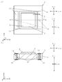
第2の実施形態における電子素子搭載用基板1において、上記した実施形態の電子素子搭載用基板1と異なる点は、平面視において、複数のビア導体13が、第2基板12の熱伝導が大きい方向(図5~図8ではy方向)に連なっている点である。なお、図7(b)において、第1基板11と第2基板12との位置関係を示すため、便宜上、第2基板12の外縁を点線で示している。
The electronic
第2の実施形態における電子素子搭載用基板1は、平面視において、第2基板12の熱伝導が大きい方向に少なくとも2つ以上のビア導体13が連なることでビア導体群13Gを形成している。図5~図8に示す例において、平面視において、3つのビア導体13が、それぞれ第2基板12の熱伝導が大きい方向に連なっており、第2基板12を挟んで第1基板11に位置した複数のビア導体群13Gを有している。第2の実施形態における電子素子搭載用基板1において、第2基板12は、平面視で複数のビア導体群13Gが第2基板12を挟んで位置した方向(図5~図8ではx方向)の熱伝導より複数のビア導体群13Gが第2基板12を挟んで位置した方向に垂直に交わる方向(図5~図8ではy方向)の熱伝導が大きくなっている(λy≒λz>>λx)。電子素子2は、図8に示す例のように、複数のビア導体13からなるビア導体群13Gに挟まれるように第2基板12の搭載部上に位置する。
In the electronic
第1基板11は、図6に示す例において、斜視にて不可視となる第1基板11の外面および貫通穴11aの内面とを点線にて示している。第2基板12は、図5、図6、図8(a)に示す例において、網掛けにて示している。図5および図8(a)に示す例において、平面視において、ビア導体13の側面と導体層14とが重なる部分を点線にて示している。
6, the outer surface of the
第2の実施形態における電子素子搭載用基板1によれば、上記した実施形態の電子素子搭載用基板1と同様に、ビア導体13から第2基板12に伝わった熱は、ビア導体13の厚み(z方向)全体において、第2基板12の外縁部から、第1基板11の外縁に沿って位置した複数のビア導体13が第2基板12を挟んで位置した方向に垂直に交わる方向に伝わるものとなり、ビア導体13から電子素子2への伝熱が抑制され、ビア導体13の熱を良好に放熱し、電子素子2の出力が低下することを抑制することができる。
According to the electronic
また、電子素子2として発光素子を用いる場合、発光素子の出力が低下することを抑制し、発光素子を良好に発光することができる電子素子搭載用基板とすることができる。
In the case where a light emitting element is used as the
また、電子素子2の熱は、第2基板12において、複数のビア導体13が第2基板12を挟んで位置した方向に垂直に交わる方向および第2基板12の厚み方向に伝わるものとなり、電子素子2の熱を良好に放熱し、電子素子2の出力が低下することを抑制することができる。
Further, the heat of the
また、第2の実施形態の電子素子搭載用基板1において、複数のビア導体13が、平面視で第2基板12の熱伝導が大きい方向に連なっており、複数のビア導体13におけるそれぞれのビア導体13の熱が第1基板11に留まりにくいものとなり、第2基板12に伝わったビア導体13の熱が、ビア導体13の厚み(z方向)全体において、第2基板12の外縁部から、第1基板11の外縁に沿って位置した複数のビア導体13が第2基板12を挟んで位置した方向に垂直に交わる方向に伝わるものとなり、ビア導体13から電子素子2への伝熱が抑制され、ビア導体13の熱を良好に放熱し、電子素子2の出力が低下することを効果的に抑制することができる。
Further, in the electronic
第1基板11は、平面視にて、方形状をしており、平面視にて、第1主面および第2主面を貫通する方形状の貫通穴11aを有している。なお、第1基板11は枠状であってもよい。第2基板12は、平面視にて方形状をしている。第1基板11の貫通穴11aの内面と2基板12の側面とを接着することにより、方形状の複合基板が形成される。なお、方形状とは、正方形状、長方形状等の四角形状である。図5~図8に示す例において、平面視にて、第1基板11および第2基板12は正方形状をしており、正方形状の複合基板が形成される。
The
また、複数のビア導体群13Gが有するビア導体13の数は、それぞれのビア導体群13Gにおいて同じであると、平面視において、第2基板12を挟んだ両側から第2基板12に伝熱するビア導体群13の熱は同等となり、熱分布が対照なものとなりやすいものとなり、ビア導体13の厚み(z方向)全体において、第2基板12の外縁部から、第1基板11の外縁に沿って位置した複数のビア導体13が第2基板12を挟んで位置した方向に垂直に交わる方向に同等に伝わるものとなり、ビア導体13から電子素子2への伝熱が抑制され、ビア導体13の熱を良好に放熱し、電子素子2の出力が低下することを効果的に抑制することができる。
Further, when the number of via
また、平面視において、第2基板12が方形状であり、複数のビア導体13(ビア導体群13G)は、第2基板12の相対する辺に沿って連なっていると、複数のビア導体13(ビア導体群13G)におけるそれぞれのビア導体13の熱が第2基板12に同等に伝わりやすいものとなり、第2基板12に伝わったビア導体群13の熱が、ビア導体13の厚み(z方向)全体において、第2基板12の外縁部から、第1基板11の外縁に沿って位置した複数のビア導体13が第2基板12を挟んで位置した方向に垂直に交わる方向に伝わるものとなり、ビア導体13から電子素子2への伝熱が抑制され、ビア導体13の熱を良好に放熱し、電子素子2の出力が低下することを効果的に抑制することができる。
Further, when the
平面視にて、第2基板12の熱伝導が大きい方向における第2基板12の両端部は、図5に示す例のように、第2基板12の熱伝導が大きい方向に連なっている複数のビア導体13のうち、端部に位置するビア導体13よりも外側に位置すると、ビア導体13から第2基板12に伝わった熱が、第2基板12の熱伝導が大きい方向における第2基板12の端部から電子素子2への伝熱が抑制され、電子素子2の出力が低下することを抑制することができる。
In plan view, both ends of the
また、図5(b)に示す例のように、第1基板11は、第1基板11の外縁に沿って位置した複数のビア導体13が第2基板12を挟んで位置した方向に垂直に交わる方向に補助層15を有していると、補助層15を、配線基板または電子素子収納用パッケージの配線導体、あるいはモジュール用基板の接続パッドに接続して、第1基板11に伝わった熱を、配線基板または電子素子収納用パッケージ、あるいはモジュール用基板に伝熱させることで、良好に放熱し、電子素子2の出力が低下することを効果的に抑制することができる。
5B, the
第2の実施形態の電子素子搭載用基板1は、その他は上述の実施形態の電子素子搭載用基板1と同様の製造方法を用いて製作することができる。
電子 The electronic
(第3の実施形態)
次に、本開示の第3の実施形態による電子装置について、図9~図12を参照しつつ説明する。
(Third embodiment)
Next, an electronic device according to a third embodiment of the present disclosure will be described with reference to FIGS.
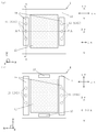
第3の実施形態における電子素子搭載用基板1において、上記した実施形態の電子素子搭載用基板1と異なる点は、第2基板12の相対する辺と、複数のビア導体13が第2基板12を挟んで位置した方向とが斜めに交わっている点である。なお、図11(b)において、第1基板11と第2基板12との位置関係を示すため、便宜上、第2基板12の外縁を点線で示している。
The electronic
第3の実施形態における電子素子搭載用基板1は、第2の実施形態の電子素子搭載用基板1と同様に、平面視において、2つ以上のビア導体13が連なることでビア導体群13Gを形成している。図9~図12において、平面視において、3つのビア導体13が、連なっており、第2基板12を挟んで第1基板11に位置した2つのビア導体群13Gを有している。
The electronic
第2基板12の相対する辺と、複数のビア導体13が第2基板12を挟んで位置した方向とが斜めに交わっているとは、第2基板12を挟んで第1基板11に位置したビア導体13を通る仮想直線N-Nと、第2基板12の相対する辺とが斜めに交わっていることを示している。
The opposite side of the
平面視において、第2基板12を挟んで第1基板11に位置した2つのビア導体群13Gは、図9~図12に示す例のように、第1基板11、第2基板12、電子素子搭載用基板1の中央部を中心とした点対称に配置されている。ビア導体13がビア導体群13Gの場合は、第2基板12を挟んで第1基板11に位置したビア導体群13Gの中心を通る仮想直線N-Nと、第2基板12の相対する辺とが斜めに交わっていることを示している。
In a plan view, the two via
第3の実施形態における電子素子搭載用基板1において、複数のビア導体群13Gが第2基板12を挟んで位置した方向の熱伝導より複数のビア導体群13Gが第2基板12を挟んで位置した方向に垂直に交わる方向の熱伝導が大きくなっている(λy≒λz>>λx)。すなわち、第2基板12を挟んで第1基板11に位置したビア導体13(ビア導体群13Gの中心)を通る仮想直線の方向より、第1基板11に位置したビア導体13(ビア導体群13Gの中心)を通る仮想直線の方向に垂直に交わる方向の熱伝導が大きくなっている(λy≒λz>>λx)。
In the electronic
第1基板11は、図10に示す例において、斜視にて不可視となる第1基板11の外面および貫通穴11aの内面とを点線にて示している。第2基板12は、図9、図10、図12(a)に示す例において、網掛けにて示している。図9および図12(a)に示す例において、平面視において、ビア導体13の側面と導体層14とが重なる部分を点線にて示している。
In the example shown in FIG. 10, the outer surface of the
第3の実施形態における電子素子搭載用基板1によれば、上記した実施形態の電子素子搭載用基板1と同様に、ビア導体13から第2基板12に伝わった熱は、ビア導体13の厚み(z方向)全体において、第2基板12の外縁部から、第1基板11の外縁に沿って位置した複数のビア導体13が第2基板12を挟んで位置した方向に垂直に交わる方向に伝わるものとなり、ビア導体13から電子素子2への伝熱が抑制され、ビア導体13の熱を良好に放熱し、電子素子2の出力が低下することを抑制することができる。
According to the electronic
また、第2基板12に伝わった熱は、第1基板11に位置したビア導体13(ビア導体群13Gの中心)を通る仮想直線の方向に垂直に交わる方向に良好に伝わるので、ビア導体群13Gにおける隣接するビア導体13の熱を良好に伝熱し、ビア導体13から電子素子2への伝熱が抑制され、ビア導体13の熱を良好に放熱し、電子素子2の出力が低下することを抑制することができる。
The heat transmitted to the
また、電子素子2として発光素子を用いる場合、発光素子の出力が低下することを抑制し、発光素子を良好に発光することができる電子素子搭載用基板とすることができる。
In the case where a light emitting element is used as the
第1基板11は、平面視にて、方形状をしており、平面視にて、第1主面および第2主面を貫通する方形状の貫通穴11aを有している。なお、第1基板11は枠状であってもよい。第2基板12は、平面視にて方形状をしている。第1基板11の貫通穴11aの内面と2基板12の側面とを接着することにより、方形状の複合基板が形成される。なお、方形状とは、正方形状、長方形状等の四角形状である。図1~図4に示す例において、平面視にて、第1基板11および第2基板12は正方形状をしており、正方形状の複合基板が形成される。
The
また、第2基板12を挟んで第1基板11に位置したビア導体13(ビア導体群13Gの中心)を通る仮想直線と第2基板12の辺とがなす角度θは、10~80度であってもよい。
The angle θ between a virtual straight line passing through the via conductor 13 (the center of the via
また、図13(a)に示す例のように、電子素子2の外辺が、第1基板11に位置したビア導体13(ビア導体群13Gの中心)を通る仮想直線N-Nの方向と垂直に交わっていると、複数のビア導体13から第2基板12に伝わった熱が、電子素子2から離れて伝わりやすいものとなり、ビア導体13から電子素子2への伝熱が抑制され、ビア導体13の熱を良好に放熱し、電子素子2の出力が低下することを抑制することができる。
Also, as in the example shown in FIG. 13A, the outer side of the
更に、図13(b)に示す例のように、それぞれの電子素子2が、第1基板11に位置したビア導体13(ビア導体群13Gの中心)同士を通る仮想直線N-Nの方向に垂直に交わる方向に対して斜めに連なって位置するように、複数の電子素子2を搭載した際には、隣接する電子素子2の方向に伝わる電子素子2の熱を抑制することでき、個々の電子素子2の出力が低下することを抑制することができる。
Further, as in the example shown in FIG. 13B, each of the
平面視にて、図12および図13に示す例のように、第1基板11に位置したビア導体13(ビア導体群13Gの中心)同士を通る仮想直線N-Nの方向に垂直に交わる方向に見た際に、複数のビア導体13が電子素子2重ならないように位置していると、ア導体13から第2基板12に伝わった熱が、電子素子2への伝熱が抑制され、電子素子2の出力が低下することを抑制することができる。
In plan view, as in the example shown in FIGS. 12 and 13, a direction perpendicular to the direction of a virtual straight line NN passing through the via conductors 13 (centers of the via
なお、図13(a)および図13(b)に示す例において、図12に示す例と同様に、平面視において、ビア導体13の側面と導体層14とが重なる部分を点線にて示している。
In the example shown in FIGS. 13 (a) and 13 (b), as in the example shown in FIG. 12, a portion where the side surface of the via
また、電子素子2として発光素子を用いる場合、発光素子の出力が低下することを抑制し、複数の発光素子を良好に発光することができる電子素子搭載用基板とすることができる。
In the case where a light-emitting element is used as the
なお、電子素子2の外辺を延長した仮想直線とビア導体13(ビア導体群13G)とが交わらないようにしておくと、ビア導体13から電子素子2への伝熱が抑制され、ビア導体13の熱を良好に放熱し、電子素子2の出力が低下することを抑制することができる。
If a virtual straight line extending the outer edge of the
第3の実施形態の電子素子搭載用基板1は、その他は上述の実施形態の電子素子搭載用基板1と同様の製造方法を用いて製作することができる。
電子 The electronic
(第4の実施形態)
次に、本開示の第4の実施形態による電子装置について、図14~図16を参照しつつ説明する。
(Fourth embodiment)
Next, an electronic device according to a fourth embodiment of the present disclosure will be described with reference to FIGS.
第4の実施形態における電子素子搭載用基板1において、上記した実施形態の電子素子搭載用基板1と異なる点は、第2基板12の第3主面または第4主面に、他の基板(第3基板16、第4基板17)を有している点である。なお、図16(b)において、第1基板11と第2基板12との位置関係を示すため、便宜上、第2基板12の外縁を点線で示している。
The electronic
第4の実施形態における電子素子搭載用基板1において、第3基板16の主面(図14~図16では上面)の第2基板12と重なる領域が、電子素子2の搭載部として用いられる。
In the electronic
第1基板11は、図14に示す例において、斜視にて不可視となる第1基板11の外面および貫通穴11aの内面とを点線にて示している。第2基板12は、図15に示す例において、網掛けにて示している。図14に示す例において、平面透視において、第2基板12の側面と、ビア導体13の側面と、導体層14とが重なる部分をそれぞれ点線にて示している。
In the example shown in FIG. 14, the outer surface of the
第4の実施形態における電子素子搭載用基板1によれば、上記した実施形態の電子素子搭載用基板1と同様に、ビア導体13から第2基板12に伝わった熱は、ビア導体13の厚み(z方向)全体において、第2基板12の外縁部から、第1基板11の外縁に沿って位置した複数のビア導体13が第2基板12を挟んで位置した方向に垂直に交わる方向に伝わるものとなり、ビア導体13から電子素子2への伝熱が抑制され、ビア導体13の熱を良好に放熱し、電子素子2の出力が低下することを抑制することができる。
According to the electronic
また、図14~図16に示す例のように、第4基板17の主面(図14~図16では下面)に、導体層14を大きく形成すると、配線基板または電子素子収納用パッケージの配線導体、あるいはモジュール用基板の接続パッドとの接合を良好にすることができ、電子素子2の熱を配線基板または電子素子収納用パッケージ、あるいはモジュール用基板へと良好に伝熱させることができる。
When the
また、電子素子2として発光素子を用いる場合、発光素子の出力が低下することを抑制し、発光素子を良好に発光することができる電子素子搭載用基板とすることができる。
In the case where a light emitting element is used as the
第1基板11は、平面視にて、方形状をしており、平面透視にて、第1主面および第2主面を貫通する方形状の貫通穴11を有している。なお、第1基板11は枠状であってもよい。第2基板12は、平面視にて方形状をしている。第3基板16は、平面視にて、方形状をしている。第4基板17は、平面視にて、方形状をしている。第1基板11の貫通穴11aの内面と第2基板12の側面とを接着し、第2基板12の第3主面と第3基板16、第2基板12の第4主面と第4基板17とを接着することにより、方形状の複合基板が形成される。また、第1基板11の第1主面と第3基板16、第1基板11の第2主面と第4基板17とを接着してもよい。なお、方形状とは、正方形状、長方形状等の四角形状である。図1~図4に示す例において、平面視にて、第1基板11および第2基板12は正方形状をしており、正方形状の複合基板が形成される。
The
第3基板16および第4基板17は、上述の第1基板11と同様の材料および方法により製作することができる。第3基板16および第4基板17の熱伝導率κ2は、第1基板11と同様に、平面方向におけるx方向とy方向とで略一定であり、第4基板14の厚み方向におけるz方向も平面方向におけるx方向とy方向と同等である(κx2≒κy2≒κz2)。例えば、第1基板16として、窒化アルミニウム質焼結体が用いられる場合、第1基板16は、100~200W/m・K程度の熱伝導率κ2である基板が用いられる。
3The
第1基板11と第2基板12が、第3基板16および第4基板17との間に位置していることから、第1基板11と第2基板12との熱膨張の違いによる電子素子搭載用基板1の歪みが抑制され、電子素子2の位置ずれ、または電子素子搭載用基板1の歪みを抑制することで良好に光を放出しやすくすることができる。
Since the
特に、第3基板16および第4基板17が、第1基板11と実質的に同一材料の絶縁体を用いている、すなわち、例えば、第1基板11として、150W/m・Kの窒化アルミニウム質焼結体を用いている場合、第3基板16および第4基板17として、150W/m・Kの窒化アルミニウム質焼結体を用いていると、より効果的に電子素子搭載用基板1の歪みを抑制することで良好に光を放出しやすくすることができる。
In particular, the
また、第3基板16の厚みT3は、例えば、50μm~500μm程度である。また、第4基板17の厚みT4は、例えば、50μm~500μm程度である。第3基板16の厚みT3と第4基板17の厚みT4とは、10%程度の範囲内において同等の厚みで設けられている(0.90T4≦T3≦1.10T4)と、より効果的に電子素子搭載用基板1の歪みを抑制することで良好に光を放出しやすくすることができる。例えば、第3基板T3の厚みが100μmである場合、第4基板17の厚みは、100μm(90μm~110μm)であってもよい。
{Circle around (3)} The thickness T3 of the
また、第3基板16の厚みT3は、第1基板11の厚みT1および第2基板12の厚みT2よりも小さく、第4基板17の厚みT4は、第1基板11の厚みT1および第2基板12の厚みT2よりも小さいと、電子素子2の熱を配線基板または電子素子収納用パッケージ、あるいはモジュール用基板へと良好に伝熱させることができ、より効果的に電子素子搭載用基板1の歪みを抑制することで良好に光を放出しやすくすることができる。
The thickness T3 of the
図14~図16に示す例において、第1基板11は正方形の枠状をしており、第2基板12、第3基板16、第4基板17は、長方形状をしており、第1基板11、第2基板12、第3基板13、第4基板14を接着することにより、長方形状の複合基板が形成される。
In the examples shown in FIGS. 14 to 16, the
第3基板16および第4基板17にも、第1基板11と同様に、ビア導体13および導体層14が設けられている。第4の実施形態の電子素子搭載用基板1において、ビア導体13および導体層14は、従来周知の薄膜法およびめっき法により形成してもよい。例えば、複合基板を形成した後、複合基板にビア導体13となる貫通孔を形成し、ビア導体13と導体層14とを形成しても構わない。
ビ ア Similarly to the
また、第3基板16または第4基板17は、図17~図19に示す例のように、第2基板12の第3主面と第4主面、さらに第1基板11の第1主面おける内縁および第2主面おける内縁を覆うように配置しても良いし、図20および図21に示す例のように、第3基板16が第1基板11の第1主面および第2基板12の第3主面を覆い、第4基板17が第1基板11の第2主面および第2基板12の第4主面を覆い、第1基板11に設けた導体層14が露出するような貫通部を第3基板16および第4基板17に設けた構成としても構わない。上記において、第3基板16および第4基板17にビア導体13および導体層14を設ける必要がないので、効率よく、電子素子搭載用基板1を形成することができる。なお、図19(b)、図21(b)において、第1基板11と第2基板12との位置関係を示すため、便宜上、第2基板12の外縁を点線で示している。
Further, the
第4の実施形態の電子素子搭載用基板1は、その他は上述の実施形態の電子素子搭載用基板1と同様の製造方法を用いて製作することができる。
電子 The electronic
本開示は、上述の実施形態の例に限定されるものではなく、種々の変更は可能である。例えば、第1の実施形態の電子素子搭載用基板~第4の実施形態の電子素子搭載用基板1において、複合基板の角部に切欠き部または面取り部を有している方形状であっても構わない。
The present disclosure is not limited to the above-described embodiments, and various modifications are possible. For example, in the electronic
また、例えば、第3の実施形態の電子素子搭載用基板1において、第4の実施形態の電子素子搭載用基板1と同様に、第2基板12の第3主面に第3基板16を配置し、第2基板12の第4主面に第4基板17を配置していても構わない。
Further, for example, in the electronic
また、上述の第1~第4の実施形態の電素素子搭載用基板1を組み合わせた電子素子搭載用基板1であっても構わない。例えば、第4の実施形態の電子素子搭載用基板1において、第3の実施形態の電子素子搭載用基板1と同様に、第2基板12の相対する辺と、複数のビア導体13が第2基板12を挟んで位置した方向とが斜めに交わっていても構わない。
The electronic
Claims (8)
平面視で該第1基板の内側に位置し、炭素材料からなり、厚み方向における前記第1主面側に位置した第3主面および該第3主面と反対側に位置する第4主面を有する第2基板と、
平面視において、該第2基板を挟んで前記第1基板に位置した複数のビア導体とを有しており、
平面視において、前記第2基板は、前記複数のビア導体が前記第2基板を挟んで位置した方向の熱伝導より前記複数のビア導体が前記第2基板を挟んで位置した方向に垂直に交わる方向の熱伝導が大きいことを特徴とする電子素子搭載用基板。 A first substrate having a first main surface and a second main surface opposite to the first main surface;
A third main surface located inside the first substrate in a plan view, made of a carbon material, and located on the first main surface side in a thickness direction, and a fourth main surface located on a side opposite to the third main surface A second substrate having:
And a plurality of via conductors located on the first substrate with the second substrate interposed therebetween in a plan view.
In a plan view, the second substrate intersects perpendicularly to a direction in which the plurality of via conductors are located across the second substrate from heat conduction in a direction in which the plurality of via conductors are located sandwiching the second substrate. A substrate for mounting an electronic element, which has a large heat conduction in a direction.
該電子素子搭載用基板の搭載部に搭載された電子素子とを有していることを特徴とする電子装置。 An electronic element mounting board according to any one of claims 1 to 5,
An electronic device mounted on a mounting portion of the electronic device mounting substrate.
該電子装置が接続されたモジュール用基板とを有することを特徴とする電子モジュール。 An electronic device according to claim 6 or claim 7,
An electronic module comprising: a module substrate to which the electronic device is connected.
Priority Applications (5)
| Application Number | Priority Date | Filing Date | Title |
|---|---|---|---|
| CN201980042360.9A CN112368825A (en) | 2018-06-26 | 2019-06-26 | Substrate for mounting electronic component, electronic device, and electronic module |
| JP2020527574A JP7025545B2 (en) | 2018-06-26 | 2019-06-26 | Boards for mounting electronic devices, electronic devices and electronic modules |
| EP19825844.4A EP3817041B1 (en) | 2018-06-26 | 2019-06-26 | Electronic element mounting substrate, electronic device, and electronic module |
| US17/254,458 US20210272868A1 (en) | 2018-06-26 | 2019-06-26 | Electronic element mounting substrate, electronic device, and electronic module |
| JP2022019951A JP7358525B2 (en) | 2018-06-26 | 2022-02-10 | Substrates for mounting electronic elements, electronic devices, and electronic modules |
Applications Claiming Priority (2)
| Application Number | Priority Date | Filing Date | Title |
|---|---|---|---|
| JP2018-120970 | 2018-06-26 | ||
| JP2018120970 | 2018-06-26 |
Publications (1)
| Publication Number | Publication Date |
|---|---|
| WO2020004459A1 true WO2020004459A1 (en) | 2020-01-02 |
Family
ID=68984884
Family Applications (1)
| Application Number | Title | Priority Date | Filing Date |
|---|---|---|---|
| PCT/JP2019/025369 Ceased WO2020004459A1 (en) | 2018-06-26 | 2019-06-26 | Electronic element mounting substrate, electronic device, and electronic module |
Country Status (5)
| Country | Link |
|---|---|
| US (1) | US20210272868A1 (en) |
| EP (1) | EP3817041B1 (en) |
| JP (2) | JP7025545B2 (en) |
| CN (1) | CN112368825A (en) |
| WO (1) | WO2020004459A1 (en) |
Families Citing this family (1)
| Publication number | Priority date | Publication date | Assignee | Title |
|---|---|---|---|---|
| CN119232106B (en) * | 2024-09-20 | 2025-12-05 | 泉州市三安集成电路有限公司 | Surface acoustic wave devices and their fabrication methods |
Citations (6)
| Publication number | Priority date | Publication date | Assignee | Title |
|---|---|---|---|---|
| JP2007073654A (en) * | 2005-09-06 | 2007-03-22 | U-Ai Electronics Corp | Printed board |
| JP2009043851A (en) * | 2007-08-07 | 2009-02-26 | Toshiba Corp | Semiconductor package |
| JP2011159662A (en) * | 2010-01-29 | 2011-08-18 | Toyota Central R&D Labs Inc | Semiconductor device |
| JP2012028520A (en) * | 2010-07-22 | 2012-02-09 | Denso Corp | Semiconductor cooling device |
| JP2012164956A (en) * | 2011-01-18 | 2012-08-30 | Napura:Kk | Electronic component support device and electronic device |
| JP2013175508A (en) | 2012-02-23 | 2013-09-05 | Kyocera Corp | Wiring board, electronic device, and manufacturing method of wiring board |
Family Cites Families (21)
| Publication number | Priority date | Publication date | Assignee | Title |
|---|---|---|---|---|
| JP4989552B2 (en) * | 2008-05-08 | 2012-08-01 | トヨタ自動車株式会社 | Electronic components |
| US8085531B2 (en) * | 2009-07-14 | 2011-12-27 | Specialty Minerals (Michigan) Inc. | Anisotropic thermal conduction element and manufacturing method |
| JP2011258755A (en) * | 2010-06-09 | 2011-12-22 | Denso Corp | Heat spreader and cooling device for heating element |
| JP5316602B2 (en) * | 2010-12-16 | 2013-10-16 | 株式会社日本自動車部品総合研究所 | Heat diffusion member joining structure, heating element cooling structure, and heat diffusion member joining method |
| JP6133854B2 (en) * | 2012-05-30 | 2017-05-24 | 京セラ株式会社 | Wiring board and electronic device |
| JP6096812B2 (en) * | 2013-01-22 | 2017-03-15 | 京セラ株式会社 | Electronic device mounting package, electronic device and imaging module |
| JP2015122351A (en) * | 2013-12-20 | 2015-07-02 | 京セラ株式会社 | Electronic component loading substrate and circuit board |
| US20160211207A1 (en) * | 2014-03-07 | 2016-07-21 | Bridge Semiconductor Corporation | Semiconductor assembly having wiring board with electrical isolator and moisture inhibiting cap incorporated therein and method of making wiring board |
| US20170263546A1 (en) * | 2014-03-07 | 2017-09-14 | Bridge Semiconductor Corporation | Wiring board with electrical isolator and base board incorporated therein and semiconductor assembly and manufacturing method thereof |
| US20180166373A1 (en) * | 2014-03-07 | 2018-06-14 | Bridge Semiconductor Corp. | Method of making wiring board with interposer and electronic component incorporated with base board |
| US20180040531A1 (en) * | 2014-03-07 | 2018-02-08 | Bridge Semiconductor Corporation | Method of making interconnect substrate having routing circuitry connected to posts and terminals |
| US20190333850A1 (en) * | 2014-03-07 | 2019-10-31 | Bridge Semiconductor Corporation | Wiring board having bridging element straddling over interfaces |
| US10420204B2 (en) * | 2014-03-07 | 2019-09-17 | Bridge Semiconductor Corporation | Wiring board having electrical isolator and moisture inhibiting cap incorporated therein and method of making the same |
| JP6626735B2 (en) * | 2016-02-22 | 2019-12-25 | 京セラ株式会社 | Electronic component mounting board, electronic device and electronic module |
| KR102565119B1 (en) * | 2016-08-25 | 2023-08-08 | 삼성전기주식회사 | Electronic component embedded substrate and manufacturing method threrof |
| US11145587B2 (en) * | 2017-05-26 | 2021-10-12 | Kyocera Corporation | Electronic component mounting substrate, electronic device, and electronic module |
| US11570882B2 (en) * | 2018-03-28 | 2023-01-31 | Kyocera Corporation | Substrate for mounting electronic element, electronic device, and electronic module |
| US10672681B2 (en) * | 2018-04-30 | 2020-06-02 | Taiwan Semiconductor Manufacturing Co., Ltd. | Semiconductor packages |
| EP3817042A4 (en) * | 2018-06-27 | 2022-04-13 | Kyocera Corporation | ELECTRONIC ELEMENT MOUNTING SUBSTRATE, ELECTRONIC DEVICE AND ELECTRONIC MODULE |
| JP2020009879A (en) * | 2018-07-06 | 2020-01-16 | 太陽誘電株式会社 | Circuit board and circuit module |
| US11582858B2 (en) * | 2018-08-29 | 2023-02-14 | Kyocera Corporation | Wiring substrate, electronic device and electronic module |
-
2019
- 2019-06-26 EP EP19825844.4A patent/EP3817041B1/en active Active
- 2019-06-26 CN CN201980042360.9A patent/CN112368825A/en active Pending
- 2019-06-26 US US17/254,458 patent/US20210272868A1/en not_active Abandoned
- 2019-06-26 WO PCT/JP2019/025369 patent/WO2020004459A1/en not_active Ceased
- 2019-06-26 JP JP2020527574A patent/JP7025545B2/en active Active
-
2022
- 2022-02-10 JP JP2022019951A patent/JP7358525B2/en active Active
Patent Citations (6)
| Publication number | Priority date | Publication date | Assignee | Title |
|---|---|---|---|---|
| JP2007073654A (en) * | 2005-09-06 | 2007-03-22 | U-Ai Electronics Corp | Printed board |
| JP2009043851A (en) * | 2007-08-07 | 2009-02-26 | Toshiba Corp | Semiconductor package |
| JP2011159662A (en) * | 2010-01-29 | 2011-08-18 | Toyota Central R&D Labs Inc | Semiconductor device |
| JP2012028520A (en) * | 2010-07-22 | 2012-02-09 | Denso Corp | Semiconductor cooling device |
| JP2012164956A (en) * | 2011-01-18 | 2012-08-30 | Napura:Kk | Electronic component support device and electronic device |
| JP2013175508A (en) | 2012-02-23 | 2013-09-05 | Kyocera Corp | Wiring board, electronic device, and manufacturing method of wiring board |
Also Published As
| Publication number | Publication date |
|---|---|
| EP3817041A1 (en) | 2021-05-05 |
| JPWO2020004459A1 (en) | 2020-01-02 |
| JP7358525B2 (en) | 2023-10-10 |
| EP3817041A4 (en) | 2022-03-23 |
| US20210272868A1 (en) | 2021-09-02 |
| CN112368825A (en) | 2021-02-12 |
| JP2022070956A (en) | 2022-05-13 |
| JP7025545B2 (en) | 2022-02-24 |
| EP3817041B1 (en) | 2023-08-16 |
Similar Documents
| Publication | Publication Date | Title |
|---|---|---|
| US11145587B2 (en) | Electronic component mounting substrate, electronic device, and electronic module | |
| US9848491B2 (en) | Wiring board, electronic device, and electronic module | |
| JP6791719B2 (en) | Substrate for mounting electronic components, electronic devices and electronic modules | |
| CN105359632B (en) | Circuit board and electronic installation | |
| WO2020004567A1 (en) | Electronic element mounting substrate, electronic device, and electronic module | |
| JP7460704B2 (en) | Composite substrate and electronic device | |
| JP7358525B2 (en) | Substrates for mounting electronic elements, electronic devices, and electronic modules | |
| JP6698826B2 (en) | Substrate for mounting electronic parts, electronic device and electronic module | |
| JP6431191B2 (en) | Wiring board, electronic device and electronic module | |
| JP6626735B2 (en) | Electronic component mounting board, electronic device and electronic module | |
| US20240203818A1 (en) | Electronic element mounting substrate, electronic device, and electronic module for improving and obtaining long-term reliability | |
| JP6983178B2 (en) | Substrate for mounting electronic devices, electronic devices and electronic modules | |
| JPWO2019189612A1 (en) | Substrate for mounting electronic elements, electronic devices and electronic modules | |
| JP2022169632A (en) | Substrates for mounting electronic elements, electronic devices and electronic modules | |
| JPWO2018097313A1 (en) | Wiring board, electronic device and electronic module | |
| JP7084134B2 (en) | Electronic device | |
| WO2018155434A1 (en) | Wiring substrate, electronic device, and electronic module | |
| JPWO2019230826A1 (en) | Substrate for mounting electronic devices, electronic devices and electronic modules | |
| WO2018155559A1 (en) | Wiring substrate, electronic device, and electronic module | |
| JP2021103739A (en) | Package for mounting electronic component, electronic apparatus, and electronic module |
Legal Events
| Date | Code | Title | Description |
|---|---|---|---|
| 121 | Ep: the epo has been informed by wipo that ep was designated in this application |
Ref document number: 19825844 Country of ref document: EP Kind code of ref document: A1 |
|
| ENP | Entry into the national phase |
Ref document number: 2020527574 Country of ref document: JP Kind code of ref document: A |
|
| NENP | Non-entry into the national phase |
Ref country code: DE |
|
| ENP | Entry into the national phase |
Ref document number: 2019825844 Country of ref document: EP Effective date: 20210126 |