WO2020005756A1 - Stabilization for privacy display - Google Patents
Stabilization for privacy display Download PDFInfo
- Publication number
- WO2020005756A1 WO2020005756A1 PCT/US2019/038466 US2019038466W WO2020005756A1 WO 2020005756 A1 WO2020005756 A1 WO 2020005756A1 US 2019038466 W US2019038466 W US 2019038466W WO 2020005756 A1 WO2020005756 A1 WO 2020005756A1
- Authority
- WO
- WIPO (PCT)
- Prior art keywords
- liquid crystal
- retarder
- crystal material
- layer
- display device
- Prior art date
- Legal status (The legal status is an assumption and is not a legal conclusion. Google has not performed a legal analysis and makes no representation as to the accuracy of the status listed.)
- Ceased
Links
Classifications
-
- G—PHYSICS
- G02—OPTICS
- G02F—OPTICAL DEVICES OR ARRANGEMENTS FOR THE CONTROL OF LIGHT BY MODIFICATION OF THE OPTICAL PROPERTIES OF THE MEDIA OF THE ELEMENTS INVOLVED THEREIN; NON-LINEAR OPTICS; FREQUENCY-CHANGING OF LIGHT; OPTICAL LOGIC ELEMENTS; OPTICAL ANALOGUE/DIGITAL CONVERTERS
- G02F1/00—Devices or arrangements for the control of the intensity, colour, phase, polarisation or direction of light arriving from an independent light source, e.g. switching, gating or modulating; Non-linear optics
- G02F1/01—Devices or arrangements for the control of the intensity, colour, phase, polarisation or direction of light arriving from an independent light source, e.g. switching, gating or modulating; Non-linear optics for the control of the intensity, phase, polarisation or colour
- G02F1/13—Devices or arrangements for the control of the intensity, colour, phase, polarisation or direction of light arriving from an independent light source, e.g. switching, gating or modulating; Non-linear optics for the control of the intensity, phase, polarisation or colour based on liquid crystals, e.g. single liquid crystal display cells
- G02F1/137—Devices or arrangements for the control of the intensity, colour, phase, polarisation or direction of light arriving from an independent light source, e.g. switching, gating or modulating; Non-linear optics for the control of the intensity, phase, polarisation or colour based on liquid crystals, e.g. single liquid crystal display cells characterised by the electro-optical or magneto-optical effect, e.g. field-induced phase transition, orientation effect, guest-host interaction or dynamic scattering
-
- G—PHYSICS
- G06—COMPUTING OR CALCULATING; COUNTING
- G06F—ELECTRIC DIGITAL DATA PROCESSING
- G06F3/00—Input arrangements for transferring data to be processed into a form capable of being handled by the computer; Output arrangements for transferring data from processing unit to output unit, e.g. interface arrangements
- G06F3/01—Input arrangements or combined input and output arrangements for interaction between user and computer
- G06F3/03—Arrangements for converting the position or the displacement of a member into a coded form
- G06F3/041—Digitisers, e.g. for touch screens or touch pads, characterised by the transducing means
- G06F3/044—Digitisers, e.g. for touch screens or touch pads, characterised by the transducing means by capacitive means
- G06F3/0445—Digitisers, e.g. for touch screens or touch pads, characterised by the transducing means by capacitive means using two or more layers of sensing electrodes, e.g. using two layers of electrodes separated by a dielectric layer
-
- G—PHYSICS
- G02—OPTICS
- G02B—OPTICAL ELEMENTS, SYSTEMS OR APPARATUS
- G02B6/00—Light guides; Structural details of arrangements comprising light guides and other optical elements, e.g. couplings
- G02B6/0001—Light guides; Structural details of arrangements comprising light guides and other optical elements, e.g. couplings specially adapted for lighting devices or systems
- G02B6/0011—Light guides; Structural details of arrangements comprising light guides and other optical elements, e.g. couplings specially adapted for lighting devices or systems the light guides being planar or of plate-like form
- G02B6/0033—Means for improving the coupling-out of light from the light guide
- G02B6/0035—Means for improving the coupling-out of light from the light guide provided on the surface of the light guide or in the bulk of it
- G02B6/0038—Linear indentations or grooves, e.g. arc-shaped grooves or meandering grooves, extending over the full length or width of the light guide
-
- G—PHYSICS
- G02—OPTICS
- G02B—OPTICAL ELEMENTS, SYSTEMS OR APPARATUS
- G02B6/00—Light guides; Structural details of arrangements comprising light guides and other optical elements, e.g. couplings
- G02B6/0001—Light guides; Structural details of arrangements comprising light guides and other optical elements, e.g. couplings specially adapted for lighting devices or systems
- G02B6/0011—Light guides; Structural details of arrangements comprising light guides and other optical elements, e.g. couplings specially adapted for lighting devices or systems the light guides being planar or of plate-like form
- G02B6/0033—Means for improving the coupling-out of light from the light guide
- G02B6/005—Means for improving the coupling-out of light from the light guide provided by one optical element, or plurality thereof, placed on the light output side of the light guide
- G02B6/0055—Reflecting element, sheet or layer
-
- G—PHYSICS
- G02—OPTICS
- G02F—OPTICAL DEVICES OR ARRANGEMENTS FOR THE CONTROL OF LIGHT BY MODIFICATION OF THE OPTICAL PROPERTIES OF THE MEDIA OF THE ELEMENTS INVOLVED THEREIN; NON-LINEAR OPTICS; FREQUENCY-CHANGING OF LIGHT; OPTICAL LOGIC ELEMENTS; OPTICAL ANALOGUE/DIGITAL CONVERTERS
- G02F1/00—Devices or arrangements for the control of the intensity, colour, phase, polarisation or direction of light arriving from an independent light source, e.g. switching, gating or modulating; Non-linear optics
- G02F1/01—Devices or arrangements for the control of the intensity, colour, phase, polarisation or direction of light arriving from an independent light source, e.g. switching, gating or modulating; Non-linear optics for the control of the intensity, phase, polarisation or colour
- G02F1/13—Devices or arrangements for the control of the intensity, colour, phase, polarisation or direction of light arriving from an independent light source, e.g. switching, gating or modulating; Non-linear optics for the control of the intensity, phase, polarisation or colour based on liquid crystals, e.g. single liquid crystal display cells
- G02F1/1323—Arrangements for providing a switchable viewing angle
-
- G—PHYSICS
- G02—OPTICS
- G02F—OPTICAL DEVICES OR ARRANGEMENTS FOR THE CONTROL OF LIGHT BY MODIFICATION OF THE OPTICAL PROPERTIES OF THE MEDIA OF THE ELEMENTS INVOLVED THEREIN; NON-LINEAR OPTICS; FREQUENCY-CHANGING OF LIGHT; OPTICAL LOGIC ELEMENTS; OPTICAL ANALOGUE/DIGITAL CONVERTERS
- G02F1/00—Devices or arrangements for the control of the intensity, colour, phase, polarisation or direction of light arriving from an independent light source, e.g. switching, gating or modulating; Non-linear optics
- G02F1/01—Devices or arrangements for the control of the intensity, colour, phase, polarisation or direction of light arriving from an independent light source, e.g. switching, gating or modulating; Non-linear optics for the control of the intensity, phase, polarisation or colour
- G02F1/13—Devices or arrangements for the control of the intensity, colour, phase, polarisation or direction of light arriving from an independent light source, e.g. switching, gating or modulating; Non-linear optics for the control of the intensity, phase, polarisation or colour based on liquid crystals, e.g. single liquid crystal display cells
- G02F1/133—Constructional arrangements; Operation of liquid crystal cells; Circuit arrangements
- G02F1/1333—Constructional arrangements; Manufacturing methods
- G02F1/13338—Input devices, e.g. touch panels
-
- G—PHYSICS
- G02—OPTICS
- G02F—OPTICAL DEVICES OR ARRANGEMENTS FOR THE CONTROL OF LIGHT BY MODIFICATION OF THE OPTICAL PROPERTIES OF THE MEDIA OF THE ELEMENTS INVOLVED THEREIN; NON-LINEAR OPTICS; FREQUENCY-CHANGING OF LIGHT; OPTICAL LOGIC ELEMENTS; OPTICAL ANALOGUE/DIGITAL CONVERTERS
- G02F1/00—Devices or arrangements for the control of the intensity, colour, phase, polarisation or direction of light arriving from an independent light source, e.g. switching, gating or modulating; Non-linear optics
- G02F1/01—Devices or arrangements for the control of the intensity, colour, phase, polarisation or direction of light arriving from an independent light source, e.g. switching, gating or modulating; Non-linear optics for the control of the intensity, phase, polarisation or colour
- G02F1/13—Devices or arrangements for the control of the intensity, colour, phase, polarisation or direction of light arriving from an independent light source, e.g. switching, gating or modulating; Non-linear optics for the control of the intensity, phase, polarisation or colour based on liquid crystals, e.g. single liquid crystal display cells
- G02F1/133—Constructional arrangements; Operation of liquid crystal cells; Circuit arrangements
- G02F1/1333—Constructional arrangements; Manufacturing methods
- G02F1/1335—Structural association of cells with optical devices, e.g. polarisers or reflectors
- G02F1/133504—Diffusing, scattering, diffracting elements
-
- G—PHYSICS
- G02—OPTICS
- G02F—OPTICAL DEVICES OR ARRANGEMENTS FOR THE CONTROL OF LIGHT BY MODIFICATION OF THE OPTICAL PROPERTIES OF THE MEDIA OF THE ELEMENTS INVOLVED THEREIN; NON-LINEAR OPTICS; FREQUENCY-CHANGING OF LIGHT; OPTICAL LOGIC ELEMENTS; OPTICAL ANALOGUE/DIGITAL CONVERTERS
- G02F1/00—Devices or arrangements for the control of the intensity, colour, phase, polarisation or direction of light arriving from an independent light source, e.g. switching, gating or modulating; Non-linear optics
- G02F1/01—Devices or arrangements for the control of the intensity, colour, phase, polarisation or direction of light arriving from an independent light source, e.g. switching, gating or modulating; Non-linear optics for the control of the intensity, phase, polarisation or colour
- G02F1/13—Devices or arrangements for the control of the intensity, colour, phase, polarisation or direction of light arriving from an independent light source, e.g. switching, gating or modulating; Non-linear optics for the control of the intensity, phase, polarisation or colour based on liquid crystals, e.g. single liquid crystal display cells
- G02F1/133—Constructional arrangements; Operation of liquid crystal cells; Circuit arrangements
- G02F1/1333—Constructional arrangements; Manufacturing methods
- G02F1/1335—Structural association of cells with optical devices, e.g. polarisers or reflectors
- G02F1/133528—Polarisers
-
- G—PHYSICS
- G02—OPTICS
- G02F—OPTICAL DEVICES OR ARRANGEMENTS FOR THE CONTROL OF LIGHT BY MODIFICATION OF THE OPTICAL PROPERTIES OF THE MEDIA OF THE ELEMENTS INVOLVED THEREIN; NON-LINEAR OPTICS; FREQUENCY-CHANGING OF LIGHT; OPTICAL LOGIC ELEMENTS; OPTICAL ANALOGUE/DIGITAL CONVERTERS
- G02F1/00—Devices or arrangements for the control of the intensity, colour, phase, polarisation or direction of light arriving from an independent light source, e.g. switching, gating or modulating; Non-linear optics
- G02F1/01—Devices or arrangements for the control of the intensity, colour, phase, polarisation or direction of light arriving from an independent light source, e.g. switching, gating or modulating; Non-linear optics for the control of the intensity, phase, polarisation or colour
- G02F1/13—Devices or arrangements for the control of the intensity, colour, phase, polarisation or direction of light arriving from an independent light source, e.g. switching, gating or modulating; Non-linear optics for the control of the intensity, phase, polarisation or colour based on liquid crystals, e.g. single liquid crystal display cells
- G02F1/133—Constructional arrangements; Operation of liquid crystal cells; Circuit arrangements
- G02F1/1333—Constructional arrangements; Manufacturing methods
- G02F1/1335—Structural association of cells with optical devices, e.g. polarisers or reflectors
- G02F1/133528—Polarisers
- G02F1/133536—Reflective polarizers
-
- G—PHYSICS
- G02—OPTICS
- G02F—OPTICAL DEVICES OR ARRANGEMENTS FOR THE CONTROL OF LIGHT BY MODIFICATION OF THE OPTICAL PROPERTIES OF THE MEDIA OF THE ELEMENTS INVOLVED THEREIN; NON-LINEAR OPTICS; FREQUENCY-CHANGING OF LIGHT; OPTICAL LOGIC ELEMENTS; OPTICAL ANALOGUE/DIGITAL CONVERTERS
- G02F1/00—Devices or arrangements for the control of the intensity, colour, phase, polarisation or direction of light arriving from an independent light source, e.g. switching, gating or modulating; Non-linear optics
- G02F1/01—Devices or arrangements for the control of the intensity, colour, phase, polarisation or direction of light arriving from an independent light source, e.g. switching, gating or modulating; Non-linear optics for the control of the intensity, phase, polarisation or colour
- G02F1/13—Devices or arrangements for the control of the intensity, colour, phase, polarisation or direction of light arriving from an independent light source, e.g. switching, gating or modulating; Non-linear optics for the control of the intensity, phase, polarisation or colour based on liquid crystals, e.g. single liquid crystal display cells
- G02F1/133—Constructional arrangements; Operation of liquid crystal cells; Circuit arrangements
- G02F1/1333—Constructional arrangements; Manufacturing methods
- G02F1/1335—Structural association of cells with optical devices, e.g. polarisers or reflectors
- G02F1/13363—Birefringent elements, e.g. for optical compensation
-
- G—PHYSICS
- G02—OPTICS
- G02F—OPTICAL DEVICES OR ARRANGEMENTS FOR THE CONTROL OF LIGHT BY MODIFICATION OF THE OPTICAL PROPERTIES OF THE MEDIA OF THE ELEMENTS INVOLVED THEREIN; NON-LINEAR OPTICS; FREQUENCY-CHANGING OF LIGHT; OPTICAL LOGIC ELEMENTS; OPTICAL ANALOGUE/DIGITAL CONVERTERS
- G02F1/00—Devices or arrangements for the control of the intensity, colour, phase, polarisation or direction of light arriving from an independent light source, e.g. switching, gating or modulating; Non-linear optics
- G02F1/01—Devices or arrangements for the control of the intensity, colour, phase, polarisation or direction of light arriving from an independent light source, e.g. switching, gating or modulating; Non-linear optics for the control of the intensity, phase, polarisation or colour
- G02F1/13—Devices or arrangements for the control of the intensity, colour, phase, polarisation or direction of light arriving from an independent light source, e.g. switching, gating or modulating; Non-linear optics for the control of the intensity, phase, polarisation or colour based on liquid crystals, e.g. single liquid crystal display cells
- G02F1/133—Constructional arrangements; Operation of liquid crystal cells; Circuit arrangements
- G02F1/1333—Constructional arrangements; Manufacturing methods
- G02F1/1335—Structural association of cells with optical devices, e.g. polarisers or reflectors
- G02F1/13363—Birefringent elements, e.g. for optical compensation
- G02F1/133634—Birefringent elements, e.g. for optical compensation the refractive index Nz perpendicular to the element surface being different from in-plane refractive indices Nx and Ny, e.g. biaxial or with normal optical axis
-
- G—PHYSICS
- G02—OPTICS
- G02F—OPTICAL DEVICES OR ARRANGEMENTS FOR THE CONTROL OF LIGHT BY MODIFICATION OF THE OPTICAL PROPERTIES OF THE MEDIA OF THE ELEMENTS INVOLVED THEREIN; NON-LINEAR OPTICS; FREQUENCY-CHANGING OF LIGHT; OPTICAL LOGIC ELEMENTS; OPTICAL ANALOGUE/DIGITAL CONVERTERS
- G02F1/00—Devices or arrangements for the control of the intensity, colour, phase, polarisation or direction of light arriving from an independent light source, e.g. switching, gating or modulating; Non-linear optics
- G02F1/01—Devices or arrangements for the control of the intensity, colour, phase, polarisation or direction of light arriving from an independent light source, e.g. switching, gating or modulating; Non-linear optics for the control of the intensity, phase, polarisation or colour
- G02F1/13—Devices or arrangements for the control of the intensity, colour, phase, polarisation or direction of light arriving from an independent light source, e.g. switching, gating or modulating; Non-linear optics for the control of the intensity, phase, polarisation or colour based on liquid crystals, e.g. single liquid crystal display cells
- G02F1/133—Constructional arrangements; Operation of liquid crystal cells; Circuit arrangements
- G02F1/1333—Constructional arrangements; Manufacturing methods
- G02F1/1335—Structural association of cells with optical devices, e.g. polarisers or reflectors
- G02F1/13363—Birefringent elements, e.g. for optical compensation
- G02F1/133638—Waveplates, i.e. plates with a retardation value of lambda/n
-
- G—PHYSICS
- G02—OPTICS
- G02F—OPTICAL DEVICES OR ARRANGEMENTS FOR THE CONTROL OF LIGHT BY MODIFICATION OF THE OPTICAL PROPERTIES OF THE MEDIA OF THE ELEMENTS INVOLVED THEREIN; NON-LINEAR OPTICS; FREQUENCY-CHANGING OF LIGHT; OPTICAL LOGIC ELEMENTS; OPTICAL ANALOGUE/DIGITAL CONVERTERS
- G02F1/00—Devices or arrangements for the control of the intensity, colour, phase, polarisation or direction of light arriving from an independent light source, e.g. switching, gating or modulating; Non-linear optics
- G02F1/01—Devices or arrangements for the control of the intensity, colour, phase, polarisation or direction of light arriving from an independent light source, e.g. switching, gating or modulating; Non-linear optics for the control of the intensity, phase, polarisation or colour
- G02F1/13—Devices or arrangements for the control of the intensity, colour, phase, polarisation or direction of light arriving from an independent light source, e.g. switching, gating or modulating; Non-linear optics for the control of the intensity, phase, polarisation or colour based on liquid crystals, e.g. single liquid crystal display cells
- G02F1/133—Constructional arrangements; Operation of liquid crystal cells; Circuit arrangements
- G02F1/1333—Constructional arrangements; Manufacturing methods
- G02F1/1337—Surface-induced orientation of the liquid crystal molecules, e.g. by alignment layers
-
- G—PHYSICS
- G02—OPTICS
- G02F—OPTICAL DEVICES OR ARRANGEMENTS FOR THE CONTROL OF LIGHT BY MODIFICATION OF THE OPTICAL PROPERTIES OF THE MEDIA OF THE ELEMENTS INVOLVED THEREIN; NON-LINEAR OPTICS; FREQUENCY-CHANGING OF LIGHT; OPTICAL LOGIC ELEMENTS; OPTICAL ANALOGUE/DIGITAL CONVERTERS
- G02F1/00—Devices or arrangements for the control of the intensity, colour, phase, polarisation or direction of light arriving from an independent light source, e.g. switching, gating or modulating; Non-linear optics
- G02F1/01—Devices or arrangements for the control of the intensity, colour, phase, polarisation or direction of light arriving from an independent light source, e.g. switching, gating or modulating; Non-linear optics for the control of the intensity, phase, polarisation or colour
- G02F1/13—Devices or arrangements for the control of the intensity, colour, phase, polarisation or direction of light arriving from an independent light source, e.g. switching, gating or modulating; Non-linear optics for the control of the intensity, phase, polarisation or colour based on liquid crystals, e.g. single liquid crystal display cells
- G02F1/133—Constructional arrangements; Operation of liquid crystal cells; Circuit arrangements
- G02F1/1333—Constructional arrangements; Manufacturing methods
- G02F1/1343—Electrodes
- G02F1/13439—Electrodes characterised by their electrical, optical, physical properties; materials therefor; method of making
-
- G—PHYSICS
- G02—OPTICS
- G02F—OPTICAL DEVICES OR ARRANGEMENTS FOR THE CONTROL OF LIGHT BY MODIFICATION OF THE OPTICAL PROPERTIES OF THE MEDIA OF THE ELEMENTS INVOLVED THEREIN; NON-LINEAR OPTICS; FREQUENCY-CHANGING OF LIGHT; OPTICAL LOGIC ELEMENTS; OPTICAL ANALOGUE/DIGITAL CONVERTERS
- G02F1/00—Devices or arrangements for the control of the intensity, colour, phase, polarisation or direction of light arriving from an independent light source, e.g. switching, gating or modulating; Non-linear optics
- G02F1/01—Devices or arrangements for the control of the intensity, colour, phase, polarisation or direction of light arriving from an independent light source, e.g. switching, gating or modulating; Non-linear optics for the control of the intensity, phase, polarisation or colour
- G02F1/13—Devices or arrangements for the control of the intensity, colour, phase, polarisation or direction of light arriving from an independent light source, e.g. switching, gating or modulating; Non-linear optics for the control of the intensity, phase, polarisation or colour based on liquid crystals, e.g. single liquid crystal display cells
- G02F1/137—Devices or arrangements for the control of the intensity, colour, phase, polarisation or direction of light arriving from an independent light source, e.g. switching, gating or modulating; Non-linear optics for the control of the intensity, phase, polarisation or colour based on liquid crystals, e.g. single liquid crystal display cells characterised by the electro-optical or magneto-optical effect, e.g. field-induced phase transition, orientation effect, guest-host interaction or dynamic scattering
- G02F1/139—Devices or arrangements for the control of the intensity, colour, phase, polarisation or direction of light arriving from an independent light source, e.g. switching, gating or modulating; Non-linear optics for the control of the intensity, phase, polarisation or colour based on liquid crystals, e.g. single liquid crystal display cells characterised by the electro-optical or magneto-optical effect, e.g. field-induced phase transition, orientation effect, guest-host interaction or dynamic scattering based on orientation effects in which the liquid crystal remains transparent
-
- G—PHYSICS
- G02—OPTICS
- G02F—OPTICAL DEVICES OR ARRANGEMENTS FOR THE CONTROL OF LIGHT BY MODIFICATION OF THE OPTICAL PROPERTIES OF THE MEDIA OF THE ELEMENTS INVOLVED THEREIN; NON-LINEAR OPTICS; FREQUENCY-CHANGING OF LIGHT; OPTICAL LOGIC ELEMENTS; OPTICAL ANALOGUE/DIGITAL CONVERTERS
- G02F1/00—Devices or arrangements for the control of the intensity, colour, phase, polarisation or direction of light arriving from an independent light source, e.g. switching, gating or modulating; Non-linear optics
- G02F1/01—Devices or arrangements for the control of the intensity, colour, phase, polarisation or direction of light arriving from an independent light source, e.g. switching, gating or modulating; Non-linear optics for the control of the intensity, phase, polarisation or colour
- G02F1/13—Devices or arrangements for the control of the intensity, colour, phase, polarisation or direction of light arriving from an independent light source, e.g. switching, gating or modulating; Non-linear optics for the control of the intensity, phase, polarisation or colour based on liquid crystals, e.g. single liquid crystal display cells
- G02F1/133—Constructional arrangements; Operation of liquid crystal cells; Circuit arrangements
- G02F1/1333—Constructional arrangements; Manufacturing methods
- G02F1/1335—Structural association of cells with optical devices, e.g. polarisers or reflectors
- G02F1/133528—Polarisers
- G02F1/133531—Polarisers characterised by the arrangement of polariser or analyser axes
-
- G—PHYSICS
- G02—OPTICS
- G02F—OPTICAL DEVICES OR ARRANGEMENTS FOR THE CONTROL OF LIGHT BY MODIFICATION OF THE OPTICAL PROPERTIES OF THE MEDIA OF THE ELEMENTS INVOLVED THEREIN; NON-LINEAR OPTICS; FREQUENCY-CHANGING OF LIGHT; OPTICAL LOGIC ELEMENTS; OPTICAL ANALOGUE/DIGITAL CONVERTERS
- G02F1/00—Devices or arrangements for the control of the intensity, colour, phase, polarisation or direction of light arriving from an independent light source, e.g. switching, gating or modulating; Non-linear optics
- G02F1/01—Devices or arrangements for the control of the intensity, colour, phase, polarisation or direction of light arriving from an independent light source, e.g. switching, gating or modulating; Non-linear optics for the control of the intensity, phase, polarisation or colour
- G02F1/13—Devices or arrangements for the control of the intensity, colour, phase, polarisation or direction of light arriving from an independent light source, e.g. switching, gating or modulating; Non-linear optics for the control of the intensity, phase, polarisation or colour based on liquid crystals, e.g. single liquid crystal display cells
- G02F1/133—Constructional arrangements; Operation of liquid crystal cells; Circuit arrangements
- G02F1/1333—Constructional arrangements; Manufacturing methods
- G02F1/1337—Surface-induced orientation of the liquid crystal molecules, e.g. by alignment layers
- G02F1/133738—Surface-induced orientation of the liquid crystal molecules, e.g. by alignment layers for homogeneous alignment
-
- G—PHYSICS
- G02—OPTICS
- G02F—OPTICAL DEVICES OR ARRANGEMENTS FOR THE CONTROL OF LIGHT BY MODIFICATION OF THE OPTICAL PROPERTIES OF THE MEDIA OF THE ELEMENTS INVOLVED THEREIN; NON-LINEAR OPTICS; FREQUENCY-CHANGING OF LIGHT; OPTICAL LOGIC ELEMENTS; OPTICAL ANALOGUE/DIGITAL CONVERTERS
- G02F1/00—Devices or arrangements for the control of the intensity, colour, phase, polarisation or direction of light arriving from an independent light source, e.g. switching, gating or modulating; Non-linear optics
- G02F1/01—Devices or arrangements for the control of the intensity, colour, phase, polarisation or direction of light arriving from an independent light source, e.g. switching, gating or modulating; Non-linear optics for the control of the intensity, phase, polarisation or colour
- G02F1/13—Devices or arrangements for the control of the intensity, colour, phase, polarisation or direction of light arriving from an independent light source, e.g. switching, gating or modulating; Non-linear optics for the control of the intensity, phase, polarisation or colour based on liquid crystals, e.g. single liquid crystal display cells
- G02F1/133—Constructional arrangements; Operation of liquid crystal cells; Circuit arrangements
- G02F1/1333—Constructional arrangements; Manufacturing methods
- G02F1/1337—Surface-induced orientation of the liquid crystal molecules, e.g. by alignment layers
- G02F1/133742—Surface-induced orientation of the liquid crystal molecules, e.g. by alignment layers for homeotropic alignment
-
- G—PHYSICS
- G02—OPTICS
- G02F—OPTICAL DEVICES OR ARRANGEMENTS FOR THE CONTROL OF LIGHT BY MODIFICATION OF THE OPTICAL PROPERTIES OF THE MEDIA OF THE ELEMENTS INVOLVED THEREIN; NON-LINEAR OPTICS; FREQUENCY-CHANGING OF LIGHT; OPTICAL LOGIC ELEMENTS; OPTICAL ANALOGUE/DIGITAL CONVERTERS
- G02F1/00—Devices or arrangements for the control of the intensity, colour, phase, polarisation or direction of light arriving from an independent light source, e.g. switching, gating or modulating; Non-linear optics
- G02F1/01—Devices or arrangements for the control of the intensity, colour, phase, polarisation or direction of light arriving from an independent light source, e.g. switching, gating or modulating; Non-linear optics for the control of the intensity, phase, polarisation or colour
- G02F1/13—Devices or arrangements for the control of the intensity, colour, phase, polarisation or direction of light arriving from an independent light source, e.g. switching, gating or modulating; Non-linear optics for the control of the intensity, phase, polarisation or colour based on liquid crystals, e.g. single liquid crystal display cells
- G02F1/137—Devices or arrangements for the control of the intensity, colour, phase, polarisation or direction of light arriving from an independent light source, e.g. switching, gating or modulating; Non-linear optics for the control of the intensity, phase, polarisation or colour based on liquid crystals, e.g. single liquid crystal display cells characterised by the electro-optical or magneto-optical effect, e.g. field-induced phase transition, orientation effect, guest-host interaction or dynamic scattering
- G02F1/13706—Devices or arrangements for the control of the intensity, colour, phase, polarisation or direction of light arriving from an independent light source, e.g. switching, gating or modulating; Non-linear optics for the control of the intensity, phase, polarisation or colour based on liquid crystals, e.g. single liquid crystal display cells characterised by the electro-optical or magneto-optical effect, e.g. field-induced phase transition, orientation effect, guest-host interaction or dynamic scattering the liquid crystal having positive dielectric anisotropy
-
- G—PHYSICS
- G02—OPTICS
- G02F—OPTICAL DEVICES OR ARRANGEMENTS FOR THE CONTROL OF LIGHT BY MODIFICATION OF THE OPTICAL PROPERTIES OF THE MEDIA OF THE ELEMENTS INVOLVED THEREIN; NON-LINEAR OPTICS; FREQUENCY-CHANGING OF LIGHT; OPTICAL LOGIC ELEMENTS; OPTICAL ANALOGUE/DIGITAL CONVERTERS
- G02F1/00—Devices or arrangements for the control of the intensity, colour, phase, polarisation or direction of light arriving from an independent light source, e.g. switching, gating or modulating; Non-linear optics
- G02F1/01—Devices or arrangements for the control of the intensity, colour, phase, polarisation or direction of light arriving from an independent light source, e.g. switching, gating or modulating; Non-linear optics for the control of the intensity, phase, polarisation or colour
- G02F1/13—Devices or arrangements for the control of the intensity, colour, phase, polarisation or direction of light arriving from an independent light source, e.g. switching, gating or modulating; Non-linear optics for the control of the intensity, phase, polarisation or colour based on liquid crystals, e.g. single liquid crystal display cells
- G02F1/137—Devices or arrangements for the control of the intensity, colour, phase, polarisation or direction of light arriving from an independent light source, e.g. switching, gating or modulating; Non-linear optics for the control of the intensity, phase, polarisation or colour based on liquid crystals, e.g. single liquid crystal display cells characterised by the electro-optical or magneto-optical effect, e.g. field-induced phase transition, orientation effect, guest-host interaction or dynamic scattering
- G02F1/13712—Devices or arrangements for the control of the intensity, colour, phase, polarisation or direction of light arriving from an independent light source, e.g. switching, gating or modulating; Non-linear optics for the control of the intensity, phase, polarisation or colour based on liquid crystals, e.g. single liquid crystal display cells characterised by the electro-optical or magneto-optical effect, e.g. field-induced phase transition, orientation effect, guest-host interaction or dynamic scattering the liquid crystal having negative dielectric anisotropy
-
- G—PHYSICS
- G02—OPTICS
- G02F—OPTICAL DEVICES OR ARRANGEMENTS FOR THE CONTROL OF LIGHT BY MODIFICATION OF THE OPTICAL PROPERTIES OF THE MEDIA OF THE ELEMENTS INVOLVED THEREIN; NON-LINEAR OPTICS; FREQUENCY-CHANGING OF LIGHT; OPTICAL LOGIC ELEMENTS; OPTICAL ANALOGUE/DIGITAL CONVERTERS
- G02F1/00—Devices or arrangements for the control of the intensity, colour, phase, polarisation or direction of light arriving from an independent light source, e.g. switching, gating or modulating; Non-linear optics
- G02F1/01—Devices or arrangements for the control of the intensity, colour, phase, polarisation or direction of light arriving from an independent light source, e.g. switching, gating or modulating; Non-linear optics for the control of the intensity, phase, polarisation or colour
- G02F1/13—Devices or arrangements for the control of the intensity, colour, phase, polarisation or direction of light arriving from an independent light source, e.g. switching, gating or modulating; Non-linear optics for the control of the intensity, phase, polarisation or colour based on liquid crystals, e.g. single liquid crystal display cells
- G02F1/137—Devices or arrangements for the control of the intensity, colour, phase, polarisation or direction of light arriving from an independent light source, e.g. switching, gating or modulating; Non-linear optics for the control of the intensity, phase, polarisation or colour based on liquid crystals, e.g. single liquid crystal display cells characterised by the electro-optical or magneto-optical effect, e.g. field-induced phase transition, orientation effect, guest-host interaction or dynamic scattering
- G02F1/13725—Devices or arrangements for the control of the intensity, colour, phase, polarisation or direction of light arriving from an independent light source, e.g. switching, gating or modulating; Non-linear optics for the control of the intensity, phase, polarisation or colour based on liquid crystals, e.g. single liquid crystal display cells characterised by the electro-optical or magneto-optical effect, e.g. field-induced phase transition, orientation effect, guest-host interaction or dynamic scattering based on guest-host interaction
-
- G—PHYSICS
- G02—OPTICS
- G02F—OPTICAL DEVICES OR ARRANGEMENTS FOR THE CONTROL OF LIGHT BY MODIFICATION OF THE OPTICAL PROPERTIES OF THE MEDIA OF THE ELEMENTS INVOLVED THEREIN; NON-LINEAR OPTICS; FREQUENCY-CHANGING OF LIGHT; OPTICAL LOGIC ELEMENTS; OPTICAL ANALOGUE/DIGITAL CONVERTERS
- G02F1/00—Devices or arrangements for the control of the intensity, colour, phase, polarisation or direction of light arriving from an independent light source, e.g. switching, gating or modulating; Non-linear optics
- G02F1/01—Devices or arrangements for the control of the intensity, colour, phase, polarisation or direction of light arriving from an independent light source, e.g. switching, gating or modulating; Non-linear optics for the control of the intensity, phase, polarisation or colour
- G02F1/13—Devices or arrangements for the control of the intensity, colour, phase, polarisation or direction of light arriving from an independent light source, e.g. switching, gating or modulating; Non-linear optics for the control of the intensity, phase, polarisation or colour based on liquid crystals, e.g. single liquid crystal display cells
- G02F1/137—Devices or arrangements for the control of the intensity, colour, phase, polarisation or direction of light arriving from an independent light source, e.g. switching, gating or modulating; Non-linear optics for the control of the intensity, phase, polarisation or colour based on liquid crystals, e.g. single liquid crystal display cells characterised by the electro-optical or magneto-optical effect, e.g. field-induced phase transition, orientation effect, guest-host interaction or dynamic scattering
- G02F1/13775—Polymer-stabilized liquid crystal layers
-
- G—PHYSICS
- G02—OPTICS
- G02F—OPTICAL DEVICES OR ARRANGEMENTS FOR THE CONTROL OF LIGHT BY MODIFICATION OF THE OPTICAL PROPERTIES OF THE MEDIA OF THE ELEMENTS INVOLVED THEREIN; NON-LINEAR OPTICS; FREQUENCY-CHANGING OF LIGHT; OPTICAL LOGIC ELEMENTS; OPTICAL ANALOGUE/DIGITAL CONVERTERS
- G02F2203/00—Function characteristic
- G02F2203/62—Switchable arrangements whereby the element being usually not switchable
-
- G—PHYSICS
- G02—OPTICS
- G02F—OPTICAL DEVICES OR ARRANGEMENTS FOR THE CONTROL OF LIGHT BY MODIFICATION OF THE OPTICAL PROPERTIES OF THE MEDIA OF THE ELEMENTS INVOLVED THEREIN; NON-LINEAR OPTICS; FREQUENCY-CHANGING OF LIGHT; OPTICAL LOGIC ELEMENTS; OPTICAL ANALOGUE/DIGITAL CONVERTERS
- G02F2413/00—Indexing scheme related to G02F1/13363, i.e. to birefringent elements, e.g. for optical compensation, characterised by the number, position, orientation or value of the compensation plates
- G02F2413/14—Negative birefingence
Definitions
- This disclosure generally relates to touch input for display devices with control of angular illumination for use in privacy display and low stray light displays.
- Privacy displays provide image visibility to a primary user (that is typically in an on-axis position) and reduced visibility of image content to a snooper, that is typically in an off-axis position.
- a privacy function may be provided by micro-louvre optical films that transmit a higher luminance from a display in an on-axis direction with lower luminance in off-axis positions, however such films are not electrically switchable, and thus the display is limited to privacy only function.
- Switchable privacy displays may be provided by control of the off-axis optical output.
- Control of off-axis privacy may be provided by means of contrast reduction, for example by adjusting the liquid crystal out of plane tilt in an In-Plane-Switching LCD.
- Control may be further provided by means of off-axis luminance reduction.
- Luminance reduction may be achieved by means of switchable backlights for a liquid crystal display (LCD) spatial light modulator.
- Off-axis luminance reduction may also be provided by switchable liquid crystal retarders, polarisers and compensation retarders arranged to modulate the input and/or output directional luminance profile of a spatial light modulator.
- Touch screens are arranged to receive input locations from observer fingers or a stylus and may comprise capacitive touch, resistive touch, electro-magnetic resonance and other known touch sensing technologies.
- a display device comprising: a spatial light modulator, a display polariser arranged on a side of the spatial light modulator, the display polariser being a linear polariser, an additional polariser arranged on the same side of the spatial light modulator as the display polariser, the additional polariser being a linear polariser, and at least one polar control retarder arranged between the additional polariser and the display polariser, wherein the at least one polar control retarder comprises a switchable liquid crystal retarder comprising: first and second support substrates; a liquid crystal layer disposed between the first and second transparent support substrates, the liquid crystal layer comprising non-cmable liquid crystal material and cured polymer material; electrodes arranged to apply a voltage for controlling the liquid crystal layer; and respective liquid crystal alignment layers supported on the first and second substrates adjacent the liquid crystal layer for aligning the non-cmable liquid crystal material.
- the cured polymer material may comprise an acrylate or a thiol material.
- Cross-linked networks may be conveniently provided within the liquid crystal layer.
- Advantageously luminance and reflectivity artefacts during applied mechanical force due to liquid crystal cell thickness variations and liquid crystal flow variations may be reduced.
- the cured polymer material may comprise a cured liquid crystal material.
- the cured liquid crystal material may comprise a reactive mesogen.
- the cured liquid crystal material may have an alignment that is aligned with the alignment of the non-curable liquid crystal material in a state in which a predetermined voltage is applied to the electrodes.
- Advantageously light scatter in one mode of operation may be reduced. Relaxation time for artefacts may be reduced. Thin flexible devices may be provided with low visibility of artefacts during folding.
- the predetermined voltage may be capable of causing the layer of cured liquid crystal material and non-curable liquid crystal material simultaneously to introduce no net relative phase shift to orthogonal polarisation components of light passed by the display polariser along an axis along a normal to the plane of the at least one polar control retarder and to introduce a net relative phase shift to orthogonal polarisation components of light passed by the additional polariser along an axis inclined to a normal to the plane of the at least one polar control retarder.
- the scatter may be reduced in a privacy mode of operation achieving increased visual security level.
- the scatter may be increased in a public mode of operation, achieving increased uniformity.
- the cured liquid crystal material may be arranged in a network that extends between the two support substrates.
- the cured liquid crystal material may be a reactive mesogen
- the ratio of the volume of the cured liquid crystal material to the volume of the non-curable liquid crystal material may be less than 5%.
- the network may be attached to each of the two support substrates.
- the electrodes may be disposed on opposite sides of the liquid crystal layer.
- a cured network may be provided that provides mechanical connection between the substrates across the area of the device.
- the optical properties of the switchable liquid crystal layer may be determined substantially by the properties of the non-curable liquid crystal material.
- a stable liquid crystal layer that provides high resistance to image artefacts arising from applied mechanical force.
- the display device may further comprise a control system arranged to control the voltage applied to the electrodes of the switchable liquid crystal retarder.
- the display may be switched between a privacy mode and a public mode of operation.
- the at least one polar control retarder may further comprise at least one passive compensation retarder.
- the switchable liquid crystal retarder may comprise two surface alignment layers disposed adjacent to the liquid crystal material on opposite sides thereof and each may be arranged to provide homeotropic alignment at the adjacent liquid crystal material.
- the layer of liquid crystal material of the switchable liquid ciystal retarder may comprise a liquid crystal material with a negative dielectric anisotropy.
- the layer of liquid crystal material may have a retardance for light of a wavelength of 550nm in a range from 500nm to 1000nm, preferably in a range from 600nm to 900nm and most preferably in a range from 700nm to 850nm.
- the at least one passive retarder may comprise at least one passive retarder having an optical axis perpendicular to the plane of the retarder, the at least one passive retarder having a total retardance for light of a wavelength of 550nm in a range from -300nm to -900nm, preferably in a range from -450nm to -800nm and most preferably in a range from -500mn to -725nm; or the at least one passive retarder comprises a pair of passive retarders which have optical axes in the plane of the retarders that are crossed, each passive retarder of the pair of passive retarders having a retardance for light of a wavelength of 550nm in a range from 300nm to 800nm, preferably in a range from 500mn to 700nm and most preferably in a range from 550mn to 675nm.
- a public mode may be provided with high image visibility over a wide polar region Power consumption for operation in public mode may be reduced.
- the switchable liquid crystal retarder may comprise two surface alignment layers disposed adjacent to the layer of liquid crystal material and on opposite sides thereof and each arranged to provide homogeneous alignment in the adjacent liquid crystal material.
- the layer of liquid crystal material of the switchable liquid crystal retarder comprises a liquid crystal material with a positive dielectric anisotropy.
- the layer of liquid crystal material may have a retardance for light of a wavelength of 550nm in a range from 500nm to 900nm, preferably in a range from 600nm to 850nm and most preferably in a range from 700nm to 800nm
- the at least one passive retarder may comprise at least one passive retarder having an optical axis perpendicular to the plane of the retarder, the at least one passive retarder having a total retardance for light of a wavelength of 550nm in a range from -300nm to -700nm, preferably in a range from -350nm to -600nm and most preferably in a range from -700nm to -500nm; or the at least one passive retarder comprises a pair of passive retarders which have optical axes in the plane of the retarders that are crossed, each passive retarder of the pair of passive retarders having a retardance for light of a wavelength of 550nm in a range from 300nm to 800n
- a method of manufacturing a switchable liquid crystal retarder which is a polar control retarder for a display device, the method comprising: providing first and second support substrates having electrodes for controlling a liquid crystal layer and having first and second liquid crystal alignment layers supported thereon for aligning liquid crystal material of the liquid ciystal layer, disposing a liquid crystal layer disposed between the first and second transparent support substrates with the first and second liquid crystal alignment layers adjacent the liquid crystal layer, the liquid crystal layer comprising non- curable liquid crystal material and curable liquid crystal material; curing the curable liquid crystal material while applying a predetermined voltage to the electrodes.
- low image scatter may be achieved in at least one mode of operation while achieving high resilience to applied mechanical force.
- the predetermined voltage may be capable of causing the layer of cured liquid crystal material and the non-curable liquid crystal material simultaneously to introduce no net relative phase shift to orthogonal polarisation components of light passed by the additional polariser along an axis along a normal to the plane of the at least one polar control retarder and to introduce a net relative phase shift to orthogonal polarisation components of light passed by the additional polariser along an axis inclined to a normal to the plane of the at least one polar control retarder.
- the predetermined voltage may be non-zero.
- the mode with low image scatter may be the privacy mode, such that the visual security level to an off-axis snooper is increased. Public mode image uniformity may be increased.
- the curable liquid crystal material may be a reactive mesogen.
- the reactive mesogen may be aligned by the applied voltage and alignment layers of the liquid crystal retarder.
- the liquid crystal layer may further comprise a polymerisation photo-initiator, and the step of curing the curable liquid crystal material is performed by applying light radiation, and preferably ultraviolet light radiation to the liquid crystal layer.
- a uniform liquid crystal layer may be provided.
- Embodiments of the present disclosure may be used in a variety of optical systems.
- the embodiment may include or work with a variety of projectors, projection systems, optical components, displays, microdisplays, computer systems, processors, self-contained projector systems, visual and/or audio-visual systems and electrical and/or optical devices.
- aspects of the present disclosure may be used with practically any apparatus related to optical and electrical devices, optical systems, presentation systems or any apparatus that may contain any type of optical system Accordingly, embodiments of the present disclosure may be employed in optical systems, devices used in visual and/or optical presentations, visual peripherals and so on and in a number of computing environments.
- Directional backlights offer control over the illumination emanating from substantially the entire output surface controlled typically through modulation of independent LED light sources arranged at the input aperture side of an optical waveguide.
- Controlling the emitted light directional distribution can achieve single person viewing for a security function, where the display can only be seen by a single viewer from a limited range of angles; high electrical efficiency, where illumination is primarily provided over a small angular directional distribution; alternating left and right eye viewing fortune sequential stereoscopic and autostereoscopic display; and low cost.
- FIGURE 1A is a schematic diagram illustrating in perspective side view a touch input display device comprising a spatial light modulator, reflective polariser and switchable liquid crystal retarder comprising a stabilised liquid crystal layer,
- FIGURE IB is a schematic diagram illustrating in front vie»' alignment of optical layers in the optical stack of FIGURE 1;
- FIGURE 2A and FIGURE 2B are schematic diagrams illustrating in a different perspective side view the touch input display device of FIGURES 1A-B in privacy and wide angle modes of operation respectively;
- FIGURE 3A is a schematic graph illustrating the variation of transmitted luminance with polar direction for transmitted light rays in FIGURE 2A in a privacy mode of operation;
- FIGURE 3B is a schematic graph illustrating the variation of reflectivity with polar direction for reflected light rays in FIGURE 2A in a privacy mode of operation;
- FIGURE 3C is a schematic graph illustrating the variation of transmitted luminance with polar direction for transmitted light rays in FIGURE 2B in a public mode of operation;
- FIGURE 3D is a schematic graph illustrating the variation of reflectivity with polar direction for reflected light rays in FIGURE 2B in a public mode of operation;
- FIGURE 4 is a schematic diagram illustrating a graph of liquid crystal director angle against fractional location through the switchable liquid crystal retarder cells of FIGURES 2A-B and FIGURES 3 A-D for different applied voltages;
- FIGURE 5A, FIGURE SB, FIGURE 5C, and FIGURE 5D are schematic diagrams illustrating in a perspective side view a method to provide a liquid crystal polymer stabilised switchable liquid crystal retarder for a privacy display comprising homogeneous alignment layers;
- FIGURE 6A is a schematic diagram illustrating in perspective side view an arrangement of a switchable compensated retarder comprising a homogeneously aligned switchable liquid crystal retarder and a negative C-plate in a privacy mode of operation;
- FIGURE 6B is a schematic diagram illustrating in perspective side view an arrangement of a switchable compensated retarder comprising a homogeneously aligned switchable liquid crystal retarder and a negative C-plate for a different applied voltage to provide operation in a public mode of operation;
- FIGURE 6C is a schematic diagram illustrating in perspective side view an arrangement of a switchable compensated retarder comprising a homogeneously aligned switchable liquid crystal retarder and a negative C-plate for no applied voltage;
- FIGURE 7A is a schematic graph illustrating the variation of transmitted luminance with polar direction for transmitted light rays in FIGURE 6B in a public mode of operation;
- FIGURE 7B is a schematic graph illustrating the variation in transmitted luminance with polar direction for transmitted light rays in FIGURE 6A in a privacy mode of operation;
- FIGURE 7C is a schematic graph illustrating the variation of reflectivity with polar direction for reflected light rays in FIGURE 6A in a privacy mode of operation
- FIGURE 8A is a schematic diagram illustrating in front perspective view observation of reflected ambient light from interface surfaces of a display of FIGURE 1 A operating in public mode;
- FIGURE 8B is a schematic diagram illustrating in front perspective view observation of reflected ambient light for the display of FIGURE 1 A operating in privacy mode;
- FIGURE 9A is a photo showing appearance of disclinations in a nematic liquid crystal layer that does not comprise the cured liquid crystal material of the present embodiments during application of pressure;
- FIGURE 9B is a photo showing appearance of disclinations in a nematic liquid crystal layer that does not comprise the cured liquid crystal material of the present embodiments shortly after release of pressure and before complete annealing of the disclinations;
- FIGURE 10A is a schematic diagram illustrating in perspective side view an arrangement of a switchable compensated retarder comprising a homeotropically aligned switchable liquid crystal retarder and a negative C-plate in a privacy mode of operation;
- FIGURE 10B is a schematic diagram illustrating a graph of liquid crystal director angle against fractional location through the switchable liquid crystal retarder cell of FIGURE 10A for no applied voltage to provide operation in a public mode of operation;
- FIGURE 11A is a schematic graph illustrating the variation of output luminance with polar direction for transmitted light rays in FIGURE 10A in a privacy mode of operation;
- FIGURE 11B is a schematic graph illustrating the variation in reflectivity with polar direction for reflected light rays in FIGURE 10 A in a privacy mode of operation
- FIGURE 11C is a schematic graph illustrating the variation of output luminance with polar direction for transmitted tight rays in FIGURE 10B in a public mode of operation;
- FIGURE 11D is a schematic graph illustrating the variation in reflectivity with polar direction for reflected tight rays in FIGURE 10B in a public mode of operation;
- FIGURE 11E is a schematic diagram illustrating a graph of liquid crystal director angle against fractional location through the switchable liquid crystal retarder cells of FIGURES 10A-B for different applied voltages;
- FIGURE 12A, FIGURE 12B, FIGURE 12C, and FIGURE 12D are schematic diagrams illustrating in a perspective side view a method to provide a liquid crystal polymer stabilised switchable liquid crystal retarder for a privacy display comprising homeo tropic alignment layers;
- FIGURE 13A is a diagram illustrating in perspective view illumination of a retarder layer by off-axis tight
- FIGURE 13B is a diagram illustrating in perspective view illumination of a retarder layer by off-axis tight of a first linear polarization state at 0 degrees;
- FIGURE 13C is a diagram illustrating in perspective view illumination of a retarder layer by off-axis tight of a first linear polarization state at 90 degrees;
- FIGURE 13D is a diagram illustrating in perspective view illumination of a retarder layer by off-axis tight of a first linear polarization state at 45 degrees;
- FIGURE 14A is a diagram illustrating in perspective view illumination of a C-plate retarder by off-axis polarised tight with a positive elevation;
- FIGURE 14B is a diagram illustrating in perspective view illumination of a C-plate retarder by off-axis polarised tight with a negative lateral angle
- FIGURE 14C is a diagram illustrating in perspective view illumination of a C-plate retarder by off-axis polarised tight with a positive elevation and negative lateral angle;
- FIGURE 14D is a diagram illustrating in perspective view illumination of a C-plate retarder by off-axis polarised tight with a positive elevation and positive lateral angle;
- FIGURE 14E is a graph illustrating the variation of output transmission with polar direction for transmitted tight rays in FIGURES 14 A-D;
- FIGURE 15A is a diagram illustrating in perspective view illumination of crossed A-plate retarder layers by off-axis polarised tight with a positive elevation;
- FIGURE 15B is a diagram illustrating in perspective view illumination of crossed A-plate retarder layers by off-axis polarised tight with a negative lateral angle;
- FIGURE 15C is a diagram illustrating in perspective view illumination of crossed A-plate retarder layers by off-axis polarised tight with a positive elevation and negative lateral angle;
- FIGURE 15D is a diagram illustrating in perspective view illumination of crossed A-plate retarder layers by off-axis polarised tight with a positive elevation and positive lateral angle; and [64] FIGURE 15E is a graph illustrating the variation of output transmission with polar direction for transmitted light rays in FIGURES 15A-D.
- optical axis of an optical retarder refers to the direction of propagation of a light ray in the uniaxial birefringent material in which no birefringence is experienced. This is different from the optical axis of an optical system which may for example be parallel to a line of symmetry or normal to a display surface along which a principal ray propagates.
- the optical axis is the slow axis when linearly polarized light with an electric vector direction parallel to the slow axis travels at the slowest speed.
- the slow' axis direction is the direction with the highest refractive index at the design wavelength.
- the fast axis direction is the direction with the lowest refractive index at the design wavelength.
- the slow axis direction is the extraordinary axis of the birefringent material.
- the fast axis direction is the extraordinary axis of the birefringent material.
- half a wavelength and quarter a wavelength refer to the operation of a retarder for a design wavelength Xothat may typically be between 500nm and 570nm.
- exemplary retardance values are provided for a wavelength of 550nm unless otherwise specified.
- the retarder provides a relative phase shift between two orthogonal polarization components of the light wave incident thereon and is characterized by the amount of relative phase, G, that it imparts on the two polarization components
- G the amount of relative phase
- the relative phase shift is related to the birefringence Dn and the thickness d of the retarder by:
- Dn is defined as the difference between the extraordinary and the ordinary index of refraction, i.e.
- G p.
- half-wave retarder herein typically refers to light propagating normal to the retarder and normal to the spatial light modulator.
- SOP state of polarisation
- a linear SOP has a polarisation component with a non-zero amplitude and an orthogonal polarisation component which has zero amplitude.
- a linear polariser transmits a unique linear SOP that has a linear polarisation component parallel to the electric vector transmission direction of the linear polariser and attenuates light with a different SOP.
- Absorbing polarisers are polarisers that absorb one polarisation component of incident light and transmit a second orthogonal polarisation component.
- Examples of absorbing linear polarisers are dichroic polarisers.
- Reflective polarisers are polarisers that reflect one polarisation component of incident light and transmit a second orthogonal polarisation component.
- Examples of reflective linear polarisers are multilayer polymeric film stacks such as DEEPTM or APFTM from 3M Corporation, or wire grid polarisers such as ProFluxTM from Moxtek.
- a retarder arranged between a linear polariser and a parallel linear analysing polariser that introduces no relative net phase shift provides full transmission of the light other than residual absorption within the linear polariser.
- a retarder that provides a relative net phase shift between orthogonal polarisation components changes the SOP and provides attenuation at the analysing polariser.
- an 'A-plate' refers to an optical retarder utilizing a layer of birefringent material with its optical axis parallel to the plane of the layer.
- a "positive A-plate” refers to positively birefringent A-plates, i.e. A-plates with a positive Dn.
- a "C-plate” refers to an optical retarder utilizing a layer of birefringent material with its optical axis perpendicular to the plane of the layer.
- a "positive C-plate” refers to positively birefringent C-plate, i.e. a C-plate with a positive Dn.
- a “negative C-plate” refers to a negatively birefringent C-plate, i.e. a C-plate with a negative Dn.
- 'O-plate' refers to an optical retarder utilizing a layer of birefringent material with its optical axis having a component parallel to the plane of the layer and a component perpendicular to the plane of the layer.
- a 'positive 'O-plate' refers to positively birefringent O-plates, i.e. O-plates with a positive Dn.
- Achromatic retarders may be provided wherein the material of the retarder is provided with a retardance Dn . d that varies with wavelength l as
- suitable materials include modified polycarbonates from Teijin Films.
- Achromatic retarders may be provided in the present embodiments to advantageously minimise colour changes between polar angular viewing directions which have low luminance reduction and polar angular viewing directions which have increased luminance reductions as will be described below.
- a liquid crystal cell has a retardance given by Dn . d where Dn is the birefringence of the liquid crystal material in the liquid crystal cell and d is the thickness of the liquid crystal cell, independent of the alignment of the liquid crystal material in the liquid crystal cell.
- Homogeneous alignment refers to the alignment of liquid crystals in switchable liquid crystal displays where molecules align substantially parallel to a substrate. Homogeneous alignment is sometimes referred to as planar alignment. Homogeneous alignment may typically be provided with a small pre-tilt such as 2 degrees, so that the molecules at the surfaces of the alignment layers of the liquid crystal cell are slightly inclined as will be described below. Pretilt is arranged to minimise degeneracies in switching of cells.
- homeotropic alignment is the state in which rod-like liquid crystalline molecules align substantially perpendicularly to the substrate.
- discotic liquid crystals homeotropic alignment is defined as the state in which an axis of the column structure, which is formed by disc-like liquid crystalline molecules, aligns perpendicularly to a surface.
- pretilt is the tilt angle of the molecules that are close to the alignment layer and is typically close to 90 degrees and for example may be 88 degrees.
- a twisted configuration also known as a helical structure or helix
- the twist may be achieved by means of a nonparallel alignment of alignment layers.
- cholesteric dopants may be added to the liquid crystal material to break degeneracy of the twist direction (clockwise or anti-clockwise) and to further control the pitch of the twist in the relaxed (typically undriven) state.
- a supertwisted liquid crystal layer has a twist of greater than 180 degrees.
- a twisted nematic layer used in spatial light modulators typically has a twist of 90 degrees.
- Liquid crystal molecules with positive dielectric anisotropy are switched from a homogeneous alignment (such as an A-plate retarder orientation) to a homeotropic alignment (such as a C-plate or O-plate retarder orientation) by means of an applied electric field.
- a homogeneous alignment such as an A-plate retarder orientation
- a homeotropic alignment such as a C-plate or O-plate retarder orientation
- Liquid crystal molecules with negative dielectric anisotropy are switched from a homeotropic alignment (such as a C-plate or O-plate retarder orientation) to a homogeneous alignment (such as an A-plate retarder orientation) by means of an applied electric field.
- a homeotropic alignment such as a C-plate or O-plate retarder orientation
- a homogeneous alignment such as an A-plate retarder orientation
- Rod-like molecules have a positive birefringence so that n e > n o as described in eqn. 2.
- Discotic molecules have negative birefringence so that n e ⁇ n o .
- Positive retarders such as A-plates, positive O-plates and positive C-plates may typically be provided by stretched films or rod-like liquid crystal molecules.
- Negative retarders such as negative C-plates may be provided by stretched films or discotic like liquid crystal molecules.
- Parallel liquid crystal cell alignment refers to the alignment direction of homogeneous alignment layers being parallel or more typically antiparallel.
- the alignment layers may have components that are substantially parallel or antiparallel.
- Hybrid aligned liquid crystal cells may have one homogeneous alignment layer and one homeotropic alignment layer. Twisted liquid crystal cells may be provided by alignment layers that do not have parallel alignment, for example oriented at 90 degrees to each other.
- Transmissive spatial light modulators may further comprise retarders between the input display polariser and the output display polariser for example as disclosed in U.S. Patent No. 8,237,876, which is herein incorporated by reference in its entirety. Such retarders (not shown) are in a different place to the passive retarders of the present embodiments. Such retarders compensate for contrast degradations for off-axis viewing locations, which is a different effect to the luminance reduction for off-axis viewing positions of the present embodiments.
- a private mode of operation of a display is one in which an observer sees a low contrast sensitivity such that an image is not clearly visible.
- Contrast sensitivity is a measure of the ability to discern between luminances of different levels in a static image.
- Inverse contrast sensitivity may be used as a measure of visual security, in that a high visual security level (VSL) corresponds to low image visibility.
- VSL is the visual security level
- Y is the luminance of the white state of the display at a snooper viewing angle
- K is the luminance of the black state of the display at the snooper viewing angle
- R is the luminance of reflected tight from the display .
- the white state transmission remains substantially constant with viewing angle.
- white state transmission typically reduces as black state transmission increases such that
- the visual security level may then be further given as:
- P is typically defined as the percentage of head-on luminance
- L at the snooper angle and the display may have image contrast ratio C and the surface reflectivity is p.
- the off-axis relative luminance, P is sometimes referred to as the privacy level.
- P describes relative luminance of a display at a given polar angle compared to head-on luminance, and is not a measure of privacy appearance.
- the display may be illuminated by Lambertian ambient illuminance I.
- a high contrast display has VSL of approximately 1.0.
- VSL increases and a private image is perceived.
- the panel contrast C is above 100:1 for almost all viewing angles, allowing the visual security level to be approximated to:
- VSL visual security level
- Switchable directional display apparatuses for use in privacy display for example and comprising plural retarders arranged between a display polariser and an additional polariser are described in U.S. Patent No. 10,126,575 and in U.S. Patent Publ. No. 2019-0086706, both of which are herein incorporated by reference in their entireties.
- Directional display apparatuses further comprising reflective polarisers arranged between the display polariser and retarders are described in U.S. Patent No. 10,303,030 U.S. and in U.S. Patent Appl. No. 16/256,120 filed January 24, 2019 (Attorney reference number 413101), both of which are herein incorporated by reference in their entireties.
- a switchable directional display apparatus comprising a switchable liquid crystal retarder arranged between a display output polariser and an additional polariser for use in displays such as privacy displays.
- FIGURE 1A is a schematic diagram illustrating in perspective side view a touch input display device 100 comprising a spatial light modulator 48, reflective polariser 302 and switchable liquid crystal retarder 300 wherein touch electrode arrays 500, 502 are provided on facing surfaces of first and second passive compensation retarders 330A, 330B; and
- FIGURE IB is a schematic diagram illustrating in front view alignment of optical layers and electrode layers in the optical stack of FIGURE 1A.
- Finger 25 location is detected by means of detection of distortion of field lines 570, 572 provided by the touch electrode arrays 500, 502 and control system comprising touch drivers 452, 454, touch controller 450 and system controller 460.
- At least one dielectric layer 504 is arranged between the switchable liquid ciystal layer 314 and the additional polariser 318.
- the first and second touch electrode arrays 500, 502 are arranged on opposite sides of the dielectric layer 504.
- a spatial light modulator 48 is a transmissive type spatial tight modulator such as a liquid crystal display and further comprises backlight 20.
- emissive displays such as OLED or micro-LED displays may be provided wherein the display 100 does not comprise input polariser 210 and backlight 20.
- the spatial tight modulator 48 is arranged to output tight 700 and comprises a display polariser 218 arranged on the output side of the spatial tight modulator 48; an additional polariser 318 arranged on the output side of the display polariser 218; a reflective polariser 302 arranged between the display polariser 218 and the additional polariser 318; and at least one retarder 300 arranged between the reflective polariser 302 and the additional polariser 318.
- the display polariser 218 and additional polariser 318 are linear polarisers.
- the display 100 is typically operated in environments with external illumination 604. Reflection of such illumination is used to provide increased visual security level to snoopers when the display operates in a privacy mode as will be described further below.
- Plural retarders 300 comprises a switchable liquid crystal retarder 301 comprising a layer 314 of non-curable liquid crystal material 414 and cured liquid crystal material 420.
- the layer 314 is arranged between transparent support substrates 312, 316 and between the display polariser 218 and the additional polariser 318.
- Electrodes 413, 415 and alignment layers 418A, 418B are arranged on the facing surfaces of support substrates 312, 316 respectively to provide electrical control and alignment respectively to the layer 314 of non-curable liquid crystal material 414.
- the control system comprises a system controller 460 that is arranged to (i) provide image data to the spatial light modulator 48 by means of spatial light modulator controller 250 (ii) provide control of the voltage driver 350 to control the drive voltage V applied to the switchable liquid crystal retarder and (iii) and to control the signal applied to and measured from the touch electrode arrays 500, 502 by means of touch controller 450 and touch drivers 452, 454.
- Reflective polariser 302 is arranged between the display polariser 218 and the plural retarders 300.
- the electric vector transmission direction 303 of the reflective polariser 302 is parallel to the electric vector transmission direction 219 of the display polariser 218 and electric vector transmission direction 319 of the additional polariser 318.
- Plural retarders 300 are arranged between the display polariser 218 and the additional polariser 318.
- Plural retarders 300 comprise: the switchable liquid crystal retarder 301 liquid crystal layer 314 arranged between input and output transparent support substrates 312, 316; and two passive compensation retarders 330A, 330B arranged between the switchable liquid crystal retarder 301 and the additional polariser 318.
- the at least one passive compensation retarder 330 comprises a pair of passive uniaxial retarders 330A, 330B having optical axes in the plane of the retarders that are crossed.
- the display polariser 218 is arranged on a side of the spatial light modulator 48, the display polariser 218 being a linear polariser.
- An additional polariser 318 is arranged on the same side of the spatial light modulator 48 as the display polariser 218, the additional polariser 318 being a linear polariser.
- the spatial light modulator is a transmissive spatial light modulator 48
- the additional polariser 318 may alternatively or additionally be arranged between backlight 20 and input polariser 210 of the spatial tight modulator.
- the spatial tight modulator 48 is an emissive spatial light modulator
- the plural retarders 300 and additional polariser 318 are arranged on the output side of the output polariser 218.
- At least one polar control retarder 300 is arranged between the additional polariser 318 and the display polariser 218, wherein the at least one polar control retarder 300 comprises a switchable liquid crystal retarder 301 comprising: first and second support substrates 312, 316; a liquid crystal layer 314 disposed between the first and second transparent support substrates 312, 316, the liquid crystal layer 314 comprising non-curable liquid crystal material 414 and cured liquid crystal material 420.
- the cured liquid crystal material may be a reactive mesogen as will be further described below.
- Electrodes 413, 415 are arranged to apply a voltage for controlling the liquid crystal layer 314; and respective liquid crystal alignment layers 418A, 418B supported on the first and second the support substrates 312, 316 adjacent the liquid crystal layer 314 for aligning the non-curable liquid crystal material 414.
- Dielectric layer 504 is arranged between the passive retarders 330A, 330B.
- the first and second touch electrode arrays 500, 502 may be provided on at least one surface of at least one passive compensation retarder 330.
- the touch electrode arrays may be arranged on the facing surfaces of the pair of passive uniaxial retarders 330A, 330B.
- the dielectric layer 504 may comprise an adhesive layer provided between the touch electrode arrays 500, 502 arranged on the facing surfaces of the pair of passive uniaxial retarders 330A, 330B.
- the dielectric layer 504 may comprise for example an optically clear adhesive (OCA) or pressure sensitive adhesive (PSA), or may be provided by another dielectric material.
- OCA optically clear adhesive
- PSA pressure sensitive adhesive
- Touching finger 25 may be near or in contact with substrate 320 that may be a glass cover or hard coated polymer layer with an oleophobic hard coating to achieve mechanical robustness and resistance to finger grease. Touch control may also be provided by a pen or stylus.
- the layer 314 comprises cured liquid crystal material 420 that is provided as a network 424 comprising cross linked bonds 422 between the molecules of the material 420.
- Spacers 370 that comprise sticky spacer balls and/or polymer walls may be provided. Advantageously some resistance to applied mechanical force may be provided. Visibility of flow of non-curable liquid crystal material 414 may be reduced.
- FIGURE IB further illustrates an arrangement of orientations of various components.
- Polarisers 218, 302, 318 are aligned with electric vector transmission directions 219, 303, 319 respectively that are parallel.
- Passive retarders 330A, 330B are provided with optical axis directions 331A, 33 IB that are at 135 degrees and 45 degrees respectively.
- the shape and orientation of electrodes 500, 502 are illustrated as orthogonal stripes, however other shapes and orientations may be provided.
- FIGURE 2A is a schematic diagram illustrating in perspective side view an arrangement of a switchable retarder 300 in a privacy mode of operation wherein the switchable retarder 301 comprises a switchable liquid crystal layer 314 with homogeneous alignment and crossed A-plate polar control passive retarders 330A, 330B; and FIGURE 2B is a schematic graph illustrating the variation of output luminance with polar direction for transmitted light rays in FIGURE 2A in a public mode of operation.
- the passive retarders 330A, 330B are composed of non-switching molecules 408A, 408B respectively.
- the switchable liquid crystal retarder 301 comprises two surface alignment layers 418A, 418B disposed adjacent to the layer 314 of non-curable liquid crystal material 414 and on opposite sides thereof and each arranged to provide homogeneous alignment in the adjacent non-curable liquid crystal material 414.
- the homogeneous alignment provides a high restoring force for the molecules of the non-curable liquid crystal material
- the switchable liquid crystal retarder 301 and passive retarders 330 may be replaced by any of those described in U.S. Patent No. 10,126,575, in U.S. Patent Publ. No. 2019-0086706, in U.S. Patent No. 10,303,030, in U.S. Patent Appl. No. 16/256,120 filed January 24, 2019 (Attorney reference number 413101), in U.S. Provisional Patent Appl. No. 62/756,902 filed November 7, 2018 (Attorney reference number 426000), and in U.S. Provisional Patent Appl. No. 62/844,980 filed May 8, 2019 (Attorney reference number 426000A), all of which are herein incorporated by reference in their entireties.
- the switchable liquid crystal layer 314 is driven by a first voltage VI in the privacy mode. Molecules of non-curable liquid crystal material 414 and cured liquid crystal material 420 are aligned with the same alignment, that is the variation of tilt of the molecules through the thickness of the layer 314 is the same for the cured material 422 and non-curable material 420.
- the switchable liquid crystal layer 314 is driven by a second voltage V2 in the public mode. Molecules of non-curable liquid crystal material 414 and cured liquid crystal material 420 are aligned with different alignments, that is the variation of tilt through the layer 314 is different for the material 420 and the material 422. The alignment of liquid crystals in the layer 314 will be described with reference to FIGURE 4.
- Some of the cured liquid crystal material 420A may be arranged in a network 424 that extends between the two support substrates 312, 316 and the network 424 is attached to each of the two support substrates 312, 316. Some of the cured liquid crystal material 420B may be arranged to be attached to the support substrates 312, 316.
- the switchable liquid crystal layer 314 the predetermined voltage VI causes the layer 314 of cured liquid crystal material 420 and the non-curable liquid crystal material 414 simultaneously to introduce no net relative phase shift to orthogonal polarisation components of light passed by the additional polariser 318 along an axis 199 along a normal to the plane of the at least one polar control retarder 300 and to introduce a net relative phase shift to orthogonal polarisation components of light passed by the additional polariser along an axis 197 inclined to a normal to the plane of the at least one polar control retarder 300.
- Such variation of phase shift when combined with passive retarders 330 and analysed by polarise rs 218, 302 and 318 provides polar variations of transmission and reflectivity such as those illustrated in FIGURES 3 A-B.
- the switchable liquid crystal layer 314 is driven by V2 that is different to the predetermined voltage VI.
- the voltage V2 causes the layer 314 of non-curable liquid crystal material 414 simultaneously to introduce no net relative phase shift to orthogonal polarisation components of light passed by the additional polariser 318 along an axis 199 along a normal to the plane of the at least one polar control retarder 300 and to introduce a substantially reduced net relative phase shift to orthogonal polarisation components of light passed by the additional polariser along an axis 197 inclined to a normal to the plane of the at least one polar control retarder 300.
- Such variation of phase shift when combined with passive retarders 330 and analysed by polarisers 218, 302 and 318 provides polar variations of transmission and reflectivity such as those illustrated in FIGURES 3C-D.
- the network 424 of cured liquid ciystal material 414 is attached to substrates 312, 316. Distortion of the thickness of the layer 314 during applied mechanical force is reduced. The retardance of the layer 314 is substantially maintained and the said net relative phase shift introduced by applied mechanical force is maintained for both privacy and public modes of operation Advantageously luminance and reflectivity artefacts in the region of the applied mechanical force are reduced. In other words, during applied force the liquid crystal layer 314 thickness may vary creating undesirable retardance profiles in the layer 314.
- the network 424 of aligned cured liquid crystal molecules 420 provides resistance to changes in the cell gap, achieving a achieving a uniform retardance profile across the display area. Advantageously the visibility of artefacts due to changes of layer 314 thickness is reduced.
- the molecules 420B that are arranged near to the substrates 312, 316 may be arranged to increase the restoring force of the molecules 414 after application of mechanical force. Advantageously visibility of artefacts may be reduced.
- non-curable liquid crystal material 414 may flow within the layer 314. Such flow may provide disclinations which adjust the retardance properties of the layer 314, and change the said net relative phase shift. Such undesirable disclinations will be illustrated in FIGURES 9A-B below in a layer not comprising cured liquid crystal material 420.
- the cured liquid crystal material 420 provides an increased restoring force for non-curable liquid crystal material 414, prevents the formation of large area disclinations and may reduce the relaxation time of disclinations after flow.
- the time for which luminance and reflectivity artefacts in the region of the applied mechanical force are visible may be reduced and the size of artefacts may be reduced.
- light scatter may be provided in the layer 314 due to the misalignment between the molecules of materials 414, 420.
- Advantageously such scatter provides increased angular luminance uniformity in public mode, increasing the image visibility for off-axis users.
- non-curable liquid crystal material 414 may occur in the liquid crystal layer 314. Flow may result in undesirable liquid crystal misalignment and dislocations that may provide visual artefacts.
- the network 424 of aligned cured liquid crystal molecules 420 provides resistance to flow of non-curable liquid crystal material 414. The amount of retardance change and disclinations in the layer 314 due to flow is reduced and advantageously the visibility of artefacts due to material flow is reduced.
- the drive voltage VI may be lower than the drive voltage V2 for the public mode as illustrated in TABLE 1 below for the embodiments of FIGURES 3A-D.
- a high drive voltage increases the restoring force and reduces the relaxation time after flow, reducing the time of artefact visibility. It is desirable to provide increased restoring force in layer 314 with lower drive voltage.
- the molecules of materials 414, 420 are aligned in the driven state for a given voltage VI and the restoring force provided by the molecules of the cured liquid crystal material 420 provides the same energy minimum as provided by the drive voltage VI.
- the total restoring force on the molecules 414 is increased, reducing the size and decay time of disclinations.
- Advantageously the visibility of artefacts is reduced.
- the voltage V2 provides a phase structure with a slow polar variation of luminance and reflectivity with polar angle as will be described in FIGURES 3C-D whereas the polar roll-off is faster in privacy mode as will be described in FIGURES 3A-B.
- Retardance variations in layer 314 from material flow in regions of applied force are visible as local luminance and reflectivity variations that depend on polar angle and distort the polar luminance and reflectivity profiles.
- the aligned cured liquid crystal material 420 provides an increased restoring force in the privacy mode of operation, reducing the range of polar angles from which the artefacts are present.
- the polar variation of visibility of material 414 flow and disclination artefacts is reduced in privacy mode and public mode.
- FIGURE 3A is a schematic graph illustrating the variation in transmission with polar direction for transmitted light rays in FIGURE 2A in a privacy mode of operation
- FIGURE 3B is a schematic graph illustrating the variation of reflectivity with polar direction for reflected light rays in FIGURE 2A in a privacy mode of operation
- FIGURE 3C is a schematic graph illustrating the variation in transmission with polar direction for transmitted light rays in FIGURE 2B in a public mode of operation
- FIGURE 3D is a schematic graph illustrating the variation of reflectivity with polar direction for reflected light rays in FIGURE 2B in a public mode of operation comprising the arrangement of TABLE 1.
- the layer 314 of non-curable liquid crystal material 414 of the switchable liquid crystal retarder 301 comprises a non-curable liquid crystal material 414 with a positive dielectric anisotropy.
- the predetermined voltage is non-zero.
- the layer 314 of non-curable liquid crystal material 414, 420 has a retardance for light of a wavelength of 550nm in a range from 500nm to 900nm, preferably in a range from 600nm to 850nm and most preferably in a range from 700nm to 800nm.
- the at least one passive retarder 330 comprises a pair of passive retarders 330A, 330B which have optical axes in the plane of the retarders that are crossed, each passive retarder 330A, 330B of the pair of passive retarders having a retardance for light of a wavelength of 550nm in a range from 300nm to 800nm, preferably in a range from 350nm to 650nm and most preferably in a range from 450nm to 550nm.
- the at least one passive retarder 330 may comprise at least one passive retarder 330 having an optical axis perpendicular to the plane of the retarder 330, the at least one passive retarder 330 having a total retardance for light of a wavelength of 550nm in a range from -300nm to -700nm, preferably in a range from -350nm to -600nm and most preferably in a ranges from -400nm to -500nm.
- the passive retarders may be provided using stretched films to advantageously achieve low cost and high uniformity.
- the passive polar control retarder 330 is provided by a pair of A-plates 330A, 330B that have crossed axes.
- ‘crossed’ refers to an angle of substantially 90° between the optical axes of the two retarders in the plane of the retarders.
- the angle between the optical axes in the plane of the retarders is at least 35° and at most 55°, more preferably at least 40° and at most 50° and most preferably at least 42.5° and at most 47.5°.
- FIGURES 3A-D illustrate that high luminance and low reflectivity are achieved in directions that are parallel to the axis 199.
- a head-on user sees a high image visibility for both privacy and public modes of operation
- FIGURES 3A-B illustrate that low luminance and high reflectivity are achieved in directions that are along axis 197 that is inclined to the axis 199 in the lateral direction for privacy operation
- Advantageously off-axis snoopers are presented with a high visual security level during privacy mode of operation
- FIGURES 3C-D illustrate that high luminance and low reflectivity are achieved in directions that are along axis 197 that is inclined to the axis 199 in the lateral direction for public operation
- Advantageously off-axis users are presented with a high image visibility during public mode of operation
- FIGURE 4 is a schematic diagram illustrating a graph of liquid crystal director angle against fractional location through the switchable liquid crystal retarder cells of FIGURES 2A-B and FIGURES 3 A-D for different applied voltages.
- Profile 441 illustrates non-curable liquid crystal material 414 tilt angle for 0V applied voltage
- tilt profile 443 illustrates director orientations for privacy mode such as an applied voltage VI of 2.5V
- tilt profile 445 illustrates director orientations for public mode such as an applied voltage V2 of 5V.
- the cured liquid crystal material 420 of the present embodiments has a profile 443 for both privacy mode and public mode.
- the non-curable liquid crystal material 414 switches between the profile 445 in public mode and 443 in private mode.
- FIGURES 5A-D are schematic diagrams illustrating in a perspective side view a method to provide a reactive mesogen polymer stabilised switchable liquid crystal retarder for a privacy display. Additional features of the arrangement of FIGURES 5A-D not discussed in further detail may be assumed to correspond to the features with equivalent reference numerals as discussed above, including any potential variations in the features.
- the liquid crystal layer may comprise the optical properties illustrated in TABLE 1, or other tables herein.
- the curable liquid crystal material 420 may be a reactive mesogen.
- a reactive mesogen is a low molecular weight liquid crystalline material containing a reactive end group that is polymerizable by visible or UV light. RMs have the intrinsic features of liquid crystals including selforganisation, anisotropic optical and dielectric properties, and controlled alignment defined by a surface alignment layer for example rubbed polyimide; at the same time, they can be polymerized in to networks structures or solid materials with their liquid crystalline alignments and anisotropic properties retained.
- example reactive mesogen material include RM257 and RM488 marketed by Merck Ltd.
- Example photo initiators include lrgacure 651 marketed by Ciba.
- the ratio of the volume of the curable liquid crystal material 420 to the volume of the non- curable liquid crystal material 414 may be less than 5%.
- Advantageously scatter may be reduced and visual security level in privacy mode increased.
- FIGURE 5A further illustrates the liquid crystal layer 314 comprising curable polymer material 421 that may be isotropic.
- the curable polymer material Prior to cure the curable polymer material may comprise monomer materials.
- Curable polymer materials 420, 421 may include materials comprising acrylates or thiols.
- FIGURE 5B illustrates that a predetermined voltage VI is applied to the electrodes 418A, 418B.
- FIGURE 5C illustrates curing the curable liquid crystal material 420 while applying the predetermined voltage VI.
- the liquid crystal material may further comprise a polymerisation photo- initiator.
- the step of curing the curable liquid crystal material is performed by applying light radiation 720 from light source 722, and preferably ultraviolet light radiation to the liquid crystal layer
- FIGURE 5D illustrates the liquid crystal retarder 301 after the curable liquid crystal material 420 is cured to provided network 424 and the voltage VI is removed.
- the non-curable liquid crystal molecules 414 ate provided with a tilt and orientation provided by the pretilt and alignment direction of the alignment layers 418A, 418B.
- the cured liquid crystal material 420 is provided by the applied voltage VI and alignment direction of the alignment layers 418A, 418B at the curing step of FIGURE
- Network 424 may comprise networks of cured liquid crystal materials 420 and cured isotropic materials 421.
- Cross linking may be provided between the cured polymer materials 420, 421 by means of bonding between the liquid crystal materials 420, between the isotropic materials 422 or between the liquid crystal materials 420 and isotropic materials 421.
- Advantageously increased resistance to applied mechanical force may be achieved.
- a method to manufacture a liquid crystal retarder for a privacy display device 100 comprises the steps of: (i) providing first and second transparent support substrates 312, 316 with electrodes 413, 415 on at least one side of each of the first and second transparent support substrates 312, 316; (ii) forming a liquid crystal alignment layer 418A, 418B on an electrode 413, 415 of each of the first and second transparent support substrates 312, 316; (iii) providing a liquid crystal layer 314 between the alignment layers; wherein the liquid crystal layer 314 comprises (a) a non-curable liquid crystal material 414 and (b) a curable liquid crystal material 420; (iv) applying a curing step voltage across the electrodes; and (v) curing the curable liquid crystal material 420.
- the curing step voltage VI is the voltage at which the liquid crystal retarder is driven to provide a privacy mode of operation of the display device (such as illustrated in FIGURE 2A).
- the curable liquid crystal material 420 comprises a photo-initiator and the step of curing the curable liquid crystal material comprises illumination by ultraviolet radiation 720.
- a switchable liquid crystal retarder 301 may be provided for use in a switchable privacy display 100 that has low visibility of artefacts due to applied pressure during touch operation.
- FIGURE 6A is a schematic diagram illustrating in perspective side view an arrangement of a switchable compensated retarder comprising a homogeneously aligned switchable liquid crystal retarder and a negative C-plate in a privacy mode of operation
- FIGURE 6B is a schematic diagram illustrating in perspective side view an arrangement of a switchable compensated retarder comprising a homogeneously aligned switchable liquid crystal retarder and a negative C-plate for a different applied voltage to provide operation in a public mode of operation
- FIGURE 6C is a schematic diagram illustrating in perspective side view an arrangement of a switchable compensated retarder comprising a homogeneously aligned switchable liquid crystal retarder and a negative C-plate for no applied voltage.
- the first and second support substrates 312, 316 may be provided by passive compensation retarders 330A, 330B.
- the passive compensation retarder 330 comprises a negative C-plate retarder having an optical axis that is a fast axis perpendicular to the plane of the retarder.
- the material 430 of the C-plate retarder may have a negative dielectric anisotropy.
- C-plates may comprise transparent birefringent materials such as: polycarbonates or reactive mesogens that are cast onto a substrate that provides homeotropic alignment for example: ZeonexTM Cycle Olefin Polymer (COP); discotic polymers; and Nitto DenkoTM double stretched polycarbonates.
- the switchable liquid crystal retarder of FIGURES 6A-C further comprise surface alignment layers 418A, 418B disposed adjacent to the layer of non-curable liquid crystal material 414 and each arranged to provide homogeneous alignment in the adjacent liquid crystal layer 314.
- the switchable liquid crystal retarder comprises two surface alignment layers 418A, 418B disposed adjacent to the layer of non-curable liquid crystal material 414 and on opposite sides thereof and each arranged to provide homogeneous alignment in the adjacent non-curable liquid crystal material 414.
- the substrates that are provided by passive compensation retarders 330A, 330B may have reduced thickness and stiffness compared to the substrates of FIGURE 1A for example, which may use a glass material for example.
- the present embodiments achieve increased resilience of the layer 314 to applied mechanical force during touch operation.
- Such displays may also be foldable or bendable.
- Advantageously increased resilience to folding or bending of the display may be achieved. Very low thickness may be achieved.
- FIGURE 7A is a schematic graph illustrating the variation of transmitted luminance with polar direction for transmitted light rays in FIGURE 6B in a public mode of operation
- FIGURE 7B is a schematic graph illustrating the variation in transmitted luminance with polar direction for transmitted light rays in FIGURE 6A in a privacy mode of operation
- FIGURE 7C is a schematic graph illustrating the variation of reflectivity with polar direction for reflected light rays in FIGURE 6A in a privacy mode of operation comprising the arrangement described in TABLE 2.
- the passive polar control retarder 330 comprises first and second C-plates 330A, 330B; and the switchable liquid crystal layer 314 is provided between the first and second C-plates 330A, 330B.
- the switchable liquid crystal retarder 301 comprises two surface alignment layers 418A, 418B disposed adjacent to the layer 314 of non-curable liquid crystal material 414 and on opposite sides thereof and each arranged to provide homogeneous alignment in the adjacent non-curable liquid crystal material 414.
- the layer of non-curable liquid crystal material 414 of the switchable liquid crystal retarder 301 comprises a non-curable liquid crystal material 414 with a positive dielectric anisotropy.
- the layer of liquid crystal material 314 has a retardance for light of a wavelength of 550nm in a range from 500nm to 1000nm, preferably in a range from 600nm to 900nm and most preferably in a range from 700nm to 850nm.
- the two passive retarders 330A, 330B each comprises a passive retarder having an optical axis perpendicular to the plane of the retarder and the total retardance of the two passive retarders for light of a wavelength of 550nm is in a range from -300nm to -700nm, preferably in a range from -350mn to -600nm and most preferably in a range from -400nm to -500nm.
- FIGURE 8A is a schematic diagram illustrating in front perspective view observation of reflected ambient light from interface surfaces of a display of FIGURE 1A operating in public mode.
- Display 100 may be provided with white regions 603 and black regions 601.
- a snooper 47 may observe an image on the display if luminance difference between the observed regions 601, 603 can be perceived.
- primary user 45 observes a full luminance images by rays 700 to viewing locations 26 that may be optical windows of a directional display.
- Snooper 47 observes reduced luminance rays 402 in viewing locations 27 that may for example be optical windows of a directional display comprising an imaging waveguide.
- Regions 26, 27 further represent on-axis and off-axis regions of polar graphs of FIGURES 3C-D.
- some light rays 404 may be reflected by the front surface of the additional polariser 318 and other surfaces of the display.
- reflectivity may be 4% for a bonded optical stack at normal incidence and approximately 5% for a bonded optical stack for 45 degrees incidence, due to Fresnel reflections at the air-polariser interface.
- a low luminance reflected image 605 of source 604 may be observed by the snooper on the front of the display 100.
- FIGURE 8B is a schematic diagram illustrating in front perspective view observation of reflected ambient light for the display of FIGURE 1A operating in privacy mode. Regions 26, 27 further represent on-axis and off-axis regions of polar graphs of FIGURES 3A-B.
- substantially higher reflected luminance is observable from reflection 606 of source 604 for the off-axis snooper 47 in off-axis location 27.
- user 45 in location 26 sees a low reflectivity image with high luminance.
- the shape and distribution of the reflected image 606 is determined by the ambient light source 604 spatial distribution but may be further determined by diffusion layers, particularly at the output surface of the additional polariser
- the image seen by user 45 has high luminance and image visibility and the image seen by snooper 47 has low luminance and high visual security level.
- FIGURE 9A is a photo showing appearance of disclinations 600 in a nematic liquid crystal layer 314 that does not comprise the cured liquid crystal material of the present embodiments during application of pressure by a finger 25; and FIGURE 9B is a photo showing appearance of disclinations 600 in a nematic liquid crystal layer that does not comprise the cured liquid crystal material of the present embodiments shortly after release of pressure and before complete annealing of the disclinations.
- FIGURE 10A is a schematic diagram illustrating in perspective side view an arrangement of a switchable compensated retarder 300 comprising a homeotropically aligned switchable liquid crystal retarder 301 and a negative C-plate 330 in a privacy mode of operation; and
- FIGURE 10B is a schematic diagram illustrating a graph of liquid crystal director angle against fractional location through the switchable liquid crystal retarder cell of FIGURE 10A for no applied voltage to provide operation in a public mode of operation.
- the substrate 316 may be provided by the retarder 330 to advantageously reduce thickness while the substrate 312 may be provided by a stiffer substrate material such as glass to increase rigidity and advantageously reduce the visibility of artefacts arising from applied force during touch operation.
- the switchable liquid crystal retarder 301 comprises two surface alignment layers 418A, 418B disposed adjacent to the non-curable liquid crystal material 414 on opposite sides thereof and arranged to provide homeotropic alignment at the adjacent non-curable liquid crystal material 414.
- the non-curable liquid crystal material 414 may be provided with a pretilt, for example 88 degrees from the horizontal to remove degeneracy of non-curable liquid crystal material 414 alignment.
- the cured liquid crystal material 420 may have the same alignment as for the non-curable liquid crystal material 420 when driven with the privacy mode voltage VI. Thus in the public mode the alignment of the materials 414, 420 is different and advantageously some scatter may be provided to increase uniformity.
- FIGURE 11A is a schematic graph illustrating the variation of output luminance with polar direction for transmitted light rays in FIGURE 10A in a privacy mode of operation
- FIGURE 11B is a schematic graph illustrating the variation in reflectivity with polar direction for reflected light rays in FIGURE 10A in a privacy mode of operation
- FIGURE 11C is a schematic graph illustrating the variation of output luminance with polar direction for transmitted light rays in FIGURE 10B in a public mode of operation
- FIGURE 11D is a schematic graph illustrating the variation in reflectivity with polar direction for reflected light rays in FIGURE 10B in a public mode of operation comprising the arrangement described in TABLE 3.
- the liquid crystal retarder alignment is provided by a homeotropic rather than homogeneous alignment
- the wide angle mode performance of FIGURES 11C-D is improved with respect to FIGURES 3C-D.
- the power consumption of the public mode is reduced because of the low drive voltage.
- the layer of liquid crystal material of the switchable liquid crystal retarder comprises a liquid crystal material with a negative dielectric anisotropy.
- the switchable liquid crystal retarder 301 comprises two surface alignment layers 418A, 418B disposed adjacent to the nan-curable liquid crystal material 414 on opposite sides thereof and each arranged to provide homeotropic alignment at the adjacent non-curable liquid crystal material
- the layer of liquid crystal material has a retardance for light of a wavelength of 550nm in a range from 500mn to 1000nm, preferably in a range from 600nm to 900nm and most preferably in a range from 700nm to 850nm
- the at least one passive retarder comprises a passive retarder having an optical axis perpendicular to the plane of the retarder, the passive retarder having a retardance for light of a wavelength of 550nm in a range from -300nm to -900nm, preferably in a range from -450nm to - 800nm and most preferably in a range from -500nm to -725nm; or (not shown) the at least one passive retarder comprises a pair of passive retarders which have optical axes in the plane of the retarders that are crossed, each passive retarder of the pair of passive retarders having a retardance for light of a wavelength of 550nm in a range from 300nm to 800nm, preferably in a range from 500nm to 700nm and most preferably in a range from 550nm to 675nm
- the switchable liquid crystal retarder 301 comprises two surface alignment layers disposed on electrodes 413, 415 and adjacent to the layer of non-curable liquid crystal material 414 and on opposite sides thereof and each arranged to provide homeotropic alignment in the adjacent non- curable liquid crystal material 414.
- the layer of non-curable liquid crystal material 414 of the switchable liquid crystal retarder 301 comprises a liquid crystal material with a negative dielectric anisotropy.
- the liquid crystal molecules 414 may be provided with a pretilt, for example 88 degrees from the horizontal to remove degeneracy in switching.
- FIGURE 1 1E is a schematic diagram illustrating a graph of liquid crystal director angle 407 against fractional location 440 through the switchable liquid crystal retarder cell, where the fractional location 440 varies between 0 for a location at the surface alignment layer 409 and 1 for a location at the surface alignment layer 411.
- FIGURE 1 IE differs from FIGURE 4 as the pretilt angle is large and reduces with applied voltage.
- the liquid crystal directors are at a tilt 407 of 88 degrees through the thickness of the cell as indicated by tilt profile 442.
- the tilt profile for the layer 314 may be the same as the profile 442.
- the compensation retarder 330 may provide correction for the pretilt direction of the switchable liquid crystal retarder 301.
- the compensation retarder 330 may alternatively have a uniform tilt angle of 90 degrees, such difference from the pretilt of the liquid crystal layer providing only small difference in off-axis viewing properties.
- the non-curable liquid crystal material 414 switches between profiles 442 in public mode and 444 in privacy mode while the cured liquid crystal material 420 maintains the profile 444 in both modes of operation.
- FIGURES 12A-D are schematic diagrams illustrating in a perspective side view a method to provide a liquid crystal polymer stabilised switchable liquid crystal retarder for a privacy display comprising homeotropic alignment layers.
- the method of FIGURES 12A-D is similar to that of FIGURES 5A-D other than the liquid crystal materials 414, 420 comprise negative dielectric anisotropy materials and homeotropic alignment layers 418A, 418B are provided.
- a method to manufacture a liquid crystal retarder for a privacy display device 100 comprises the steps of: (i) providing first and second transparent support substrates 312, 316 with electrodes 413, 415 on at least one side of each of the first and second transparent support substrates 312, 316; (ii) forming a liquid crystal alignment layer on an electrode 413, 415 of each of the first and second transparent support substrates 312, 316; (iii) providing a liquid crystal layer 314 between the alignment layers; wherein the liquid crystal layer 314 comprises (a) a non-curable liquid crystal material 414 and (b) a cured liquid crystal material 420; and the liquid crystal layer 314 has a retardance for light of a wavelength of 550nm in a range from 500nm to 1000nm, preferably in a range from 600nm to 900nm and most preferably in a range from 700nm to 850nm; (iv) applying a curing step voltage across the electrodes; and (v) curing the curable
- the curing step voltage VI is the voltage at which the liquid crystal retarder is driven to provide a privacy mode of operation of the display device (such as illustrated in FIGURE 2A).
- the curable liquid crystal material 420 comprises a photo-initiator and the step of curing the curable liquid crystal material comprises illumination by ultraviolet radiation 720.
- a liquid crystal layer is provided, wherein the liquid crystal material comprises non-curable liquid crystal molecules 414 and curable liquid crystal molecules 420.
- Alignment layers are arranged to provide alignment, such as homogeneous alignment at each surface by means of anti-parallel pre-tilt alignments.
- a voltage may be applied across the liquid crystal layer 413 by means of electrodes 413, 415.
- the voltage may be substantially the same voltage VI provided to achieve the liquid crystal alignment state for privacy operation.
- the cell may be cured while the voltage remains applied.
- Curable liquid crystal material 420 may comprise for example reactive mesogen molecules, with a similar birefringence to that of the non-curable liquid crystal material 414 and a photo initiator.
- FIGURE 12D after cure the light source 722 and voltage driver are removed and the molecules of the non-curable liquid crystal material 414 relax while the molecules of the cured liquid crystal material 420 remain in the cured liquid crystal network 424 comprising the molecular orientation of the driven state.
- the at least one polar control retarder is configured so that it does not affect the luminance of light passing through the reflective polariser 318, the at least one polar control retarder, and the additional polariser 218 along an axis along a normal to the plane of the polar control retarder(s) but it does reduce the luminance of light passing through the reflective polariser 318, the at least one polar control retarder, and the additional polariser 218 along an axis inclined to a normal to the plane of the polar control retarder(s), at least in one of the switchable states of the compensated switchable polar control polar control retarder 300.
- FIGURE 13A is a schematic diagram illustrating in perspective view illumination of a polar control retarder layer by off-axis light.
- Polar control retarder 630 may comprise birefnngent material, represented by refractive index ellipsoid 632 with optical axis direction 634 at 0 degrees to the x-axis, and have a thickness 631.
- Normal light rays 636 propagate so that the path length in the material is the same as the thickness 631.
- Light rays 637 are in the y-z plane have an increased path length; however the birefringence of the material is substantially the same as the rays 636.
- fight rays 638 that are in the x-z plane have an increased path length in the birefnngent material and further the birefringence is different to the normal ray 636.
- the retardance of the polar control retarder 630 is thus dependent on the angle of incidence of the respective ray, and also the plane of incidence, that is rays 638 in the x-z will have a retardance different from the normal rays 636 and the rays 637 in the y-z plane.
- FIGURE 13B is a schematic diagram illustrating in perspective view illumination of a polar control retarder layer by off-axis fight of a third linear polarization state at 90 degrees to the x-axis
- FIGURE 13C is a schematic diagram illustrating in perspective view illumination of a polar control retarder layer by off-axis light of a fourth linear polarization state at 0 degrees to the x-axis.
- the incident linear polarization states are aligned to the optical axes of the birefringent material, represented by ellipse 632.
- the polar control retarder 630 introduces no phase shift to polarisation components of light passed by the polariser on the input side of the polar control retarder 630 along an axis along a normal to the plane of the polar control retarder 630. Accordingly, the polar control retarder 630 does not affect the luminance of light passing through the polar control retarder 630 and polatisers (not shown) on each side of the polar control retarder 630.
- FIGURES 29A-C relate specifically to the polar control retarder 630 that is passive, a similar effect is achieved by the polar control retarders in the devices described above.
- FIGURE 13D is a schematic diagram illustrating in perspective view illumination of a polar control retarder 630 layer by off-axis light of a linear polarization state at 45 degrees.
- the linear polarization state may be resolved into third and fourth polarization components that are respectively orthogonal and parallel to optical axis 634 direction
- the polar control retarder thickness 631 and material retardance represented by refractive index ellipsoid 632 may provide a net effect of relatively shifting the phase of the third and fourth polarization components incident thereon in a normal direction represented by ray 636 by half a wavelength, for a design wavelength
- the design wavelength may for example be in the range of 500 to 550 nm.
- the output polarization may be rotated by 90 degrees to a linear polarization state 640 at -45 degrees.
- Light propagating along ray 637 may see a phase difference that is similar but not identical to the phase difference along ray 637 due to the change in thickness, and thus an elliptical polarization state 639 may be output which may have a major axis similar to the linear polarization axis of the output light for ray 636.
- phase difference for the incident linear polarization state along ray 638 may be significantly different, in particular a lower phase difference may be provided.
- phase difference may provide an output polarization state 644 that is substantially circular at a given inclination angle 642.
- the polar control retarder 630 introduces a phase shift to polarisation components of light passed by the polariser on the input side of the polar control retarder 630 along an axis corresponding to ray 638 that is inclined to a normal to the plane of the polar control retarder 630.
- FIGURE 29D relates to the polar control retarder 630 that is passive, a similar effect is achieved by the polar control retarders described above, in a switchable state of the switchable liquid crystal polar control retarder corresponding to the privacy mode.
- the angular luminance control of C-plates 330A, 330B between an additional polariser 318 and output display polariser 218 will now be described for various off-axis illumination arrangements with reference to the operation of a C-plate between the parallel polarisers 500, 210 will now be described.
- FIGURE 14A is a schematic diagram illustrating in perspective view illumination of a C- plate layer by off-axis polarised light with a positive elevation Incident linear polarisation component 704 is incident onto the birefringent material 632 of the polar control retarder 560 that is a C-plate with optical axis direction 507 that is perpendicular to the plane of the polar control retarder 560.
- Polarisation component 704 sees no net phase difference on transmission through the liquid crystal molecule and so the output polarisation component is the same as component 704. Thus a maximum transmission is seen through the polariser 210.
- the polar control retarder 560 having an optical axis perpendicular to the plane of the polar control retarder comprises a C-plate.
- FIGURE 14B is a schematic diagram illustrating in perspective view illumination of a C- plate layer by off-axis polarised light with a negative lateral angle.
- polarisation state 704 sees no net phase difference and is transmitted with maximum luminance.
- the polar control retarder 560 introduces no phase shift to polarisation components of light passed by the polariser on the input side of the polar control retarder 560 along an axis along a normal to the plane of the polar control retarder 560. Accordingly, the polar control retarder 560 does not affect the luminance of light passing through the polar control retarder 560 and polarisers (not shown) on each side of the polar control retarder 560.
- FIGURES 29A-C relate specifically to the polar control retarder 560 that is passive, a similar effect is achieved by the polar control retarders in the devices described above.
- FIGURE 14C is a schematic diagram illustrating in perspective view illumination of a C- plate layer by off-axis polarised light with a positive elevation and negative lateral angle.
- the polarisation state 704 resolves onto eigenstates 703, 705 with respect to the birefringent material 632 providing a net phase difference on transmission through the polar control retarder 560.
- the resultant elliptical polarisation component 656 is transmitted through polariser 210 with reduced luminance in comparison to the rays illustrated in FIGURES 14A-B.
- FIGURE 14D is a schematic diagram illustrating in perspective view illumination of a C- plate layer by off-axis polarised light with a positive elevation and positive lateral angle.
- the polarisation component 704 is resolved into eigenstates 703, 705 that undergo a net phase difference, and elliptical polarisation component 660 is provided, which after transmission through the polariser reduces the luminance of the respective off-axis ray.
- the polar control retarder 560 introduces a phase shift to polarisation components of light passed by the polariser on the input side of the polar control retarder 560 along an axis that is inclined to a normal to the plane of the polar control retarder 560.
- FIGURE 29D relates to the polar control retarder 560 that is passive, a similar effect is achieved by the polar control retarders described above, in a switchable state of the switchable liquid crystal polar control retarder corresponding to the privacy mode.
- FIGURE 14E is a schematic graph illustrating the variation of output transmission with polar direction for transmitted light rays in FIGURES 14A-D.
- the C-plate may provide luminance reduction in polar quadrants.
- removal of luminance reduction of the C-plate may be provided in a first wide angle state of operation
- extended polar region for luminance reduction may be achieved in a second privacy state of operation.
- FIGURE 15A is a schematic diagram illustrating in perspective view illumination of crossed A-plate retarder layers by off-axis polarised light with a positive elevation
- Linear polariser 218 with electric vector transmission direction 219 is used to provide a linear polarisation state 704 that is parallel to the lateral direction onto first A-plate 330A of the crossed A-plates 330A, 330B.
- the optical axis direction 331A is inclined at +45 degrees to the lateral direction
- the retardance of the polar control retarder 330A for the off-axis angle q 1 in the positive elevation direction provides a resultant polarisation component 650 that is generally elliptical on output.
- Polarisation component 650 is incident onto the second A-plate 330B of the crossed A-plates 330A, 330B that has an optical axis direction 33 IB that is orthogonal to the optical axis direction 331 A of the first A-plate 330A.
- the retardance of the second A-plate 330B for the off-axis angle q 1 is equal and opposite to the retardance of the first A-plate 330A.
- the output polarisation component is the same as the input polarisation component 704.
- the output polarisation component is aligned to the electric vector transmission direction of the additional polariser 318, and thus is transmitted efficiently.
- FIGURE 15B is a schematic diagram illustrating in perspective view illumination of crossed A-plate retarder layers by off-axis polarised light with a negative lateral angle.
- input polarisation component is converted by the first A-plate 330A to an intermediate polarisation component 652 that is generally an elliptical polarisation state.
- the second A-plate 330B again provides an equal and opposite retardation to the first A-plate so that the output polarisation component is the same as the input polarisation component 704 and light is efficiently transmitted through the polariser 318.
- the polar control retarder comprises a pair of retarders 330A, 330B which have optical axes in the plane of the retarders 330A, 330B that are crossed, that is the x-y plane in the present embodiments.
- the pair of retarders 330A, 330B have optical axes 331 A, 33 IB that each extend at 45° with respect to an electric vector transmission direction that is parallel to the electric vector transmission of the polariser 318.
- FIGURE 15C is a schematic diagram illustrating in perspective view illumination of crossed A-plate retarder layers by off-axis polarised light with a positive elevation and negative lateral angle.
- Polarisation component 704 is converted to an elliptical polarisation component 654 by first A-plate 330A.
- a resultant elliptical component 656 is output from the second A-plate 330B.
- Elliptical component 656 is analysed by input polariser 318 with reduced luminance in comparison to the input luminance of the first polarisation component 704.
- FIGURE 15D is a schematic diagram illustrating in perspective view illumination of crossed A-plate retarder layers by off-axis polarised light with a positive elevation and positive lateral angle.
- Polarisation components 658 and 660 are provided by first and second A-plates 330A, 330B as net retardance of first and second retarders does not provide compensation.
- luminance is reduced for light rays that have non-zero lateral angle and non-zero elevation components.
- Advantageously display privacy can be increased for snoopers that are arranged in viewing quadrants while luminous efficiency for primary display users is not substantially reduced.
- FIGURE 15E is a schematic graph illustrating the variation of output transmission with polar direction for transmitted light rays in FIGURES 15A-D.
- the area of luminance reduction is increased for off-axis viewing.
- the switchable liquid crystal layer 314 may provide reduced uniformity in comparison to the C-plate arrangements for off-axis viewing in the first public mode state of operation
- the terms“substantially” and“approximately” provide an industry- accepted tolerance for its corresponding term and/or relativity between items. Such an industry- accepted tolerance ranges from zero percent to ten percent and corresponds to, but is not limited to, component values, angles, et cetera. Such relativity between items ranges between approximately zero percent to ten percent
Landscapes
- Physics & Mathematics (AREA)
- Nonlinear Science (AREA)
- General Physics & Mathematics (AREA)
- Optics & Photonics (AREA)
- Chemical & Material Sciences (AREA)
- Crystallography & Structural Chemistry (AREA)
- Mathematical Physics (AREA)
- Engineering & Computer Science (AREA)
- Theoretical Computer Science (AREA)
- General Engineering & Computer Science (AREA)
- Liquid Crystal (AREA)
- Spectroscopy & Molecular Physics (AREA)
- Human Computer Interaction (AREA)
Abstract
A display comprises a polarised output spatial light modulator, switchable liquid crystal retarder, absorbing polariser and touch panel electrodes. The switchable liquid crystal layer is stabilised by a cured reactive mesogen material during application of an applied voltage. Light scatter in privacy mode is reduced and visual security level enhanced. Visibility of disclinations during application of applied pressure, for example from a finger on a touch screen is minimised.
Description
Stabilization for privacy display
TECHNICAL FIELD
[01] This disclosure generally relates to touch input for display devices with control of angular illumination for use in privacy display and low stray light displays.
BACKGROUND
[02] Privacy displays provide image visibility to a primary user (that is typically in an on-axis position) and reduced visibility of image content to a snooper, that is typically in an off-axis position. A privacy function may be provided by micro-louvre optical films that transmit a higher luminance from a display in an on-axis direction with lower luminance in off-axis positions, however such films are not electrically switchable, and thus the display is limited to privacy only function.
[03] Switchable privacy displays may be provided by control of the off-axis optical output.
[04] Control of off-axis privacy may be provided by means of contrast reduction, for example by adjusting the liquid crystal out of plane tilt in an In-Plane-Switching LCD.
[05] Control may be further provided by means of off-axis luminance reduction. Luminance reduction may be achieved by means of switchable backlights for a liquid crystal display (LCD) spatial light modulator. Off-axis luminance reduction may also be provided by switchable liquid crystal retarders, polarisers and compensation retarders arranged to modulate the input and/or output directional luminance profile of a spatial light modulator.
[06] Touch screens are arranged to receive input locations from observer fingers or a stylus and may comprise capacitive touch, resistive touch, electro-magnetic resonance and other known touch sensing technologies.
BRIEF SUMMARY
[07] According to a first aspect of the present disclosure there is provided a display device comprising: a spatial light modulator, a display polariser arranged on a side of the spatial light modulator, the display polariser being a linear polariser, an additional polariser arranged on the same side of the spatial light modulator as the display polariser, the additional polariser being a linear polariser, and at least one polar control retarder arranged between the additional polariser and the display polariser, wherein the at least one polar control retarder comprises a switchable liquid crystal retarder comprising: first and second support substrates; a liquid crystal layer disposed between the first and second transparent support substrates, the liquid crystal layer comprising non-cmable liquid crystal material and cured polymer material; electrodes arranged to apply a voltage for controlling the liquid crystal layer; and respective liquid crystal alignment layers supported on the first and second substrates adjacent the liquid crystal layer for aligning the non-cmable liquid crystal material. The
cured polymer material may comprise an acrylate or a thiol material. Cross-linked networks may be conveniently provided within the liquid crystal layer. Advantageously luminance and reflectivity artefacts during applied mechanical force due to liquid crystal cell thickness variations and liquid crystal flow variations may be reduced.
[08] The cured polymer material may comprise a cured liquid crystal material. The cured liquid crystal material may comprise a reactive mesogen. The cured liquid crystal material may have an alignment that is aligned with the alignment of the non-curable liquid crystal material in a state in which a predetermined voltage is applied to the electrodes. Advantageously light scatter in one mode of operation may be reduced. Relaxation time for artefacts may be reduced. Thin flexible devices may be provided with low visibility of artefacts during folding.
[09] The predetermined voltage may be capable of causing the layer of cured liquid crystal material and non-curable liquid crystal material simultaneously to introduce no net relative phase shift to orthogonal polarisation components of light passed by the display polariser along an axis along a normal to the plane of the at least one polar control retarder and to introduce a net relative phase shift to orthogonal polarisation components of light passed by the additional polariser along an axis inclined to a normal to the plane of the at least one polar control retarder. Advantageously the scatter may be reduced in a privacy mode of operation achieving increased visual security level. The scatter may be increased in a public mode of operation, achieving increased uniformity.
[10] The cured liquid crystal material may be arranged in a network that extends between the two support substrates. The cured liquid crystal material may be a reactive mesogen The ratio of the volume of the cured liquid crystal material to the volume of the non-curable liquid crystal material may be less than 5%. The network may be attached to each of the two support substrates. The electrodes may be disposed on opposite sides of the liquid crystal layer. A cured network may be provided that provides mechanical connection between the substrates across the area of the device. The optical properties of the switchable liquid crystal layer may be determined substantially by the properties of the non-curable liquid crystal material. Advantageously a stable liquid crystal layer that provides high resistance to image artefacts arising from applied mechanical force.
[11] The display device may further comprise a control system arranged to control the voltage applied to the electrodes of the switchable liquid crystal retarder. Advantageously the display may be switched between a privacy mode and a public mode of operation.
[12] The at least one polar control retarder may further comprise at least one passive compensation retarder. Advantageously the polar region in which high visual security level for an off axis snooper is extended.
[13] The switchable liquid crystal retarder may comprise two surface alignment layers disposed adjacent to the liquid crystal material on opposite sides thereof and each may be arranged to provide homeotropic alignment at the adjacent liquid crystal material. The layer of liquid crystal material of
the switchable liquid ciystal retarder may comprise a liquid crystal material with a negative dielectric anisotropy. The layer of liquid crystal material may have a retardance for light of a wavelength of 550nm in a range from 500nm to 1000nm, preferably in a range from 600nm to 900nm and most preferably in a range from 700nm to 850nm. The at least one passive retarder may comprise at least one passive retarder having an optical axis perpendicular to the plane of the retarder, the at least one passive retarder having a total retardance for light of a wavelength of 550nm in a range from -300nm to -900nm, preferably in a range from -450nm to -800nm and most preferably in a range from -500mn to -725nm; or the at least one passive retarder comprises a pair of passive retarders which have optical axes in the plane of the retarders that are crossed, each passive retarder of the pair of passive retarders having a retardance for light of a wavelength of 550nm in a range from 300nm to 800nm, preferably in a range from 500mn to 700nm and most preferably in a range from 550mn to 675nm. Advantageously a public mode may be provided with high image visibility over a wide polar region Power consumption for operation in public mode may be reduced.
[14] The switchable liquid crystal retarder may comprise two surface alignment layers disposed adjacent to the layer of liquid crystal material and on opposite sides thereof and each arranged to provide homogeneous alignment in the adjacent liquid crystal material. The layer of liquid crystal material of the switchable liquid crystal retarder comprises a liquid crystal material with a positive dielectric anisotropy. The layer of liquid crystal material may have a retardance for light of a wavelength of 550nm in a range from 500nm to 900nm, preferably in a range from 600nm to 850nm and most preferably in a range from 700nm to 800nm The at least one passive retarder may comprise at least one passive retarder having an optical axis perpendicular to the plane of the retarder, the at least one passive retarder having a total retardance for light of a wavelength of 550nm in a range from -300nm to -700nm, preferably in a range from -350nm to -600nm and most preferably in a range from -700nm to -500nm; or the at least one passive retarder comprises a pair of passive retarders which have optical axes in the plane of the retarders that are crossed, each passive retarder of the pair of passive retarders having a retardance for light of a wavelength of 550nm in a range from 300nm to 800nm, preferably in a range from 350nm to 650nm and most preferably in a range from 450nm to 550nm. Advantageously increased stability to applied mechanical force in comparison to homeotropic alignment may be achieved. In privacy mode a large polar region with high visual security level may be achieved. Thin flexible switchable retarders may be provided with high resilience to applied mechanical force.
[15] According to a second aspect of the present disclosure there is provided a method of manufacturing a switchable liquid crystal retarder which is a polar control retarder for a display device, the method comprising: providing first and second support substrates having electrodes for controlling a liquid crystal layer and having first and second liquid crystal alignment layers supported thereon for aligning liquid crystal material of the liquid ciystal layer, disposing a liquid crystal layer
disposed between the first and second transparent support substrates with the first and second liquid crystal alignment layers adjacent the liquid crystal layer, the liquid crystal layer comprising non- curable liquid crystal material and curable liquid crystal material; curing the curable liquid crystal material while applying a predetermined voltage to the electrodes. Advantageously in operation low image scatter may be achieved in at least one mode of operation while achieving high resilience to applied mechanical force.
[16] The predetermined voltage may be capable of causing the layer of cured liquid crystal material and the non-curable liquid crystal material simultaneously to introduce no net relative phase shift to orthogonal polarisation components of light passed by the additional polariser along an axis along a normal to the plane of the at least one polar control retarder and to introduce a net relative phase shift to orthogonal polarisation components of light passed by the additional polariser along an axis inclined to a normal to the plane of the at least one polar control retarder. The predetermined voltage may be non-zero. Advantageously the mode with low image scatter may be the privacy mode, such that the visual security level to an off-axis snooper is increased. Public mode image uniformity may be increased.
[17] The curable liquid crystal material may be a reactive mesogen. Advantageously the reactive mesogen may be aligned by the applied voltage and alignment layers of the liquid crystal retarder.
[18] The liquid crystal layer may further comprise a polymerisation photo-initiator, and the step of curing the curable liquid crystal material is performed by applying light radiation, and preferably ultraviolet light radiation to the liquid crystal layer. Advantageously a uniform liquid crystal layer may be provided.
[19] Embodiments of the present disclosure may be used in a variety of optical systems. The embodiment may include or work with a variety of projectors, projection systems, optical components, displays, microdisplays, computer systems, processors, self-contained projector systems, visual and/or audio-visual systems and electrical and/or optical devices. Aspects of the present disclosure may be used with practically any apparatus related to optical and electrical devices, optical systems, presentation systems or any apparatus that may contain any type of optical system Accordingly, embodiments of the present disclosure may be employed in optical systems, devices used in visual and/or optical presentations, visual peripherals and so on and in a number of computing environments.
[20] Before proceeding to the disclosed embodiments in detail, it should be understood that the disclosure is not limited in its application or creation to the details of the particular arrangements shown, because the disclosure is capable of other embodiments. Moreover, aspects of the disclosure may be set forth in different combinations and arrangements to define embodiments unique in their own right. Also, the terminology used herein is for the purpose of description and not of limitation
[21] Directional backlights offer control over the illumination emanating from substantially the entire output surface controlled typically through modulation of independent LED light sources arranged at the input aperture side of an optical waveguide. Controlling the emitted light directional distribution can achieve single person viewing for a security function, where the display can only be seen by a single viewer from a limited range of angles; high electrical efficiency, where illumination is primarily provided over a small angular directional distribution; alternating left and right eye viewing fortune sequential stereoscopic and autostereoscopic display; and low cost.
[22] These and other advantages and features of the present disclosure will become apparent to those of ordinary skill in the art upon reading this disclosure in its entirety.
BRIEF DESCRIPTION OF THE DRAWINGS
[23] Embodiments are illustrated by way of example in the accompanying FIGURES, in which like reference numbers indicate similar parts, and in which:
[24] FIGURE 1A is a schematic diagram illustrating in perspective side view a touch input display device comprising a spatial light modulator, reflective polariser and switchable liquid crystal retarder comprising a stabilised liquid crystal layer,
[25] FIGURE IB is a schematic diagram illustrating in front vie»' alignment of optical layers in the optical stack of FIGURE 1;
[26] FIGURE 2A and FIGURE 2B are schematic diagrams illustrating in a different perspective side view the touch input display device of FIGURES 1A-B in privacy and wide angle modes of operation respectively;
[27] FIGURE 3A is a schematic graph illustrating the variation of transmitted luminance with polar direction for transmitted light rays in FIGURE 2A in a privacy mode of operation;
[28] FIGURE 3B is a schematic graph illustrating the variation of reflectivity with polar direction for reflected light rays in FIGURE 2A in a privacy mode of operation;
[29] FIGURE 3C is a schematic graph illustrating the variation of transmitted luminance with polar direction for transmitted light rays in FIGURE 2B in a public mode of operation;
[30] FIGURE 3D is a schematic graph illustrating the variation of reflectivity with polar direction for reflected light rays in FIGURE 2B in a public mode of operation;
[31] FIGURE 4 is a schematic diagram illustrating a graph of liquid crystal director angle against fractional location through the switchable liquid crystal retarder cells of FIGURES 2A-B and FIGURES 3 A-D for different applied voltages;
[32] FIGURE 5A, FIGURE SB, FIGURE 5C, and FIGURE 5D are schematic diagrams illustrating in a perspective side view a method to provide a liquid crystal polymer stabilised switchable liquid crystal retarder for a privacy display comprising homogeneous alignment layers;
[33] FIGURE 6A is a schematic diagram illustrating in perspective side view an arrangement of a switchable compensated retarder comprising a homogeneously aligned switchable liquid crystal retarder and a negative C-plate in a privacy mode of operation;
[34] FIGURE 6B is a schematic diagram illustrating in perspective side view an arrangement of a switchable compensated retarder comprising a homogeneously aligned switchable liquid crystal retarder and a negative C-plate for a different applied voltage to provide operation in a public mode of operation;
[35] FIGURE 6C is a schematic diagram illustrating in perspective side view an arrangement of a switchable compensated retarder comprising a homogeneously aligned switchable liquid crystal retarder and a negative C-plate for no applied voltage;
[36] FIGURE 7A is a schematic graph illustrating the variation of transmitted luminance with polar direction for transmitted light rays in FIGURE 6B in a public mode of operation;
[37] FIGURE 7B is a schematic graph illustrating the variation in transmitted luminance with polar direction for transmitted light rays in FIGURE 6A in a privacy mode of operation;
[38] FIGURE 7C is a schematic graph illustrating the variation of reflectivity with polar direction for reflected light rays in FIGURE 6A in a privacy mode of operation;
[39] FIGURE 8A is a schematic diagram illustrating in front perspective view observation of reflected ambient light from interface surfaces of a display of FIGURE 1 A operating in public mode;
[40] FIGURE 8B is a schematic diagram illustrating in front perspective view observation of reflected ambient light for the display of FIGURE 1 A operating in privacy mode;
[41] FIGURE 9A is a photo showing appearance of disclinations in a nematic liquid crystal layer that does not comprise the cured liquid crystal material of the present embodiments during application of pressure;
[42] FIGURE 9B is a photo showing appearance of disclinations in a nematic liquid crystal layer that does not comprise the cured liquid crystal material of the present embodiments shortly after release of pressure and before complete annealing of the disclinations;
[43] FIGURE 10A is a schematic diagram illustrating in perspective side view an arrangement of a switchable compensated retarder comprising a homeotropically aligned switchable liquid crystal retarder and a negative C-plate in a privacy mode of operation;
[44] FIGURE 10B is a schematic diagram illustrating a graph of liquid crystal director angle against fractional location through the switchable liquid crystal retarder cell of FIGURE 10A for no applied voltage to provide operation in a public mode of operation;
[45] FIGURE 11A is a schematic graph illustrating the variation of output luminance with polar direction for transmitted light rays in FIGURE 10A in a privacy mode of operation;
[46] FIGURE 11B is a schematic graph illustrating the variation in reflectivity with polar direction for reflected light rays in FIGURE 10 A in a privacy mode of operation;
[47] FIGURE 11C is a schematic graph illustrating the variation of output luminance with polar direction for transmitted tight rays in FIGURE 10B in a public mode of operation;
[48] FIGURE 11D is a schematic graph illustrating the variation in reflectivity with polar direction for reflected tight rays in FIGURE 10B in a public mode of operation;
[49] FIGURE 11E is a schematic diagram illustrating a graph of liquid crystal director angle against fractional location through the switchable liquid crystal retarder cells of FIGURES 10A-B for different applied voltages;
[50] FIGURE 12A, FIGURE 12B, FIGURE 12C, and FIGURE 12D are schematic diagrams illustrating in a perspective side view a method to provide a liquid crystal polymer stabilised switchable liquid crystal retarder for a privacy display comprising homeo tropic alignment layers;
[51] FIGURE 13A is a diagram illustrating in perspective view illumination of a retarder layer by off-axis tight;
[52] FIGURE 13B is a diagram illustrating in perspective view illumination of a retarder layer by off-axis tight of a first linear polarization state at 0 degrees;
[53] FIGURE 13C is a diagram illustrating in perspective view illumination of a retarder layer by off-axis tight of a first linear polarization state at 90 degrees;
[54] FIGURE 13D is a diagram illustrating in perspective view illumination of a retarder layer by off-axis tight of a first linear polarization state at 45 degrees;
[55] FIGURE 14A is a diagram illustrating in perspective view illumination of a C-plate retarder by off-axis polarised tight with a positive elevation;
[56] FIGURE 14B is a diagram illustrating in perspective view illumination of a C-plate retarder by off-axis polarised tight with a negative lateral angle;
[57] FIGURE 14C is a diagram illustrating in perspective view illumination of a C-plate retarder by off-axis polarised tight with a positive elevation and negative lateral angle;
[58] FIGURE 14D is a diagram illustrating in perspective view illumination of a C-plate retarder by off-axis polarised tight with a positive elevation and positive lateral angle;
[59] FIGURE 14E is a graph illustrating the variation of output transmission with polar direction for transmitted tight rays in FIGURES 14 A-D;
[60] FIGURE 15A is a diagram illustrating in perspective view illumination of crossed A-plate retarder layers by off-axis polarised tight with a positive elevation;
[61] FIGURE 15B is a diagram illustrating in perspective view illumination of crossed A-plate retarder layers by off-axis polarised tight with a negative lateral angle;
[62] FIGURE 15C is a diagram illustrating in perspective view illumination of crossed A-plate retarder layers by off-axis polarised tight with a positive elevation and negative lateral angle;
[63] FIGURE 15D is a diagram illustrating in perspective view illumination of crossed A-plate retarder layers by off-axis polarised tight with a positive elevation and positive lateral angle; and
[64] FIGURE 15E is a graph illustrating the variation of output transmission with polar direction for transmitted light rays in FIGURES 15A-D.
DETAILED DESCRIPTION
[65] Terms related to optical retarders for the purposes of the present disclosure will now' be described.
[66] In a layer comprising a uniaxial birefringent material there is a direction governing the optical anisotropy whereas all directions perpendicular to it (or at a given angle to it) have equivalent birefringence.
[67] The optical axis of an optical retarder refers to the direction of propagation of a light ray in the uniaxial birefringent material in which no birefringence is experienced. This is different from the optical axis of an optical system which may for example be parallel to a line of symmetry or normal to a display surface along which a principal ray propagates.
[68] For light propagating in a direction orthogonal to the optical axis, the optical axis is the slow axis when linearly polarized light with an electric vector direction parallel to the slow axis travels at the slowest speed. The slow' axis direction is the direction with the highest refractive index at the design wavelength. Similarly the fast axis direction is the direction with the lowest refractive index at the design wavelength.
[69] For positive dielectric anisotropy uniaxial birefringent materials the slow axis direction is the extraordinary axis of the birefringent material. For negative dielectric anisotropy uniaxial birefringent materials the fast axis direction is the extraordinary axis of the birefringent material.
[70] The terms half a wavelength and quarter a wavelength refer to the operation of a retarder for a design wavelength Xothat may typically be between 500nm and 570nm. In the present illustrative embodiments exemplary retardance values are provided for a wavelength of 550nm unless otherwise specified.
[71] The retarder provides a relative phase shift between two orthogonal polarization components of the light wave incident thereon and is characterized by the amount of relative phase, G, that it imparts on the two polarization components In some contexts, the term“phase shift” is used without the word“relative” but still meaning relative phase shift The relative phase shift is related to the birefringence Dn and the thickness d of the retarder by:

[72] In eqa 1, Dn is defined as the difference between the extraordinary and the ordinary index of refraction, i.e.
 [73] For a half-wave retarder, the relationship between d, Dn, and l0 is chosen so that the phase shift between polarization components is G = p. For a quarter-wave retarder, the relationship between d, Dn, and l0 is chosen so that the phase shift between polarization components is G = p/2.
[74] The term half-wave retarder herein typically refers to light propagating normal to the retarder and normal to the spatial light modulator.
[75] Some aspects of the propagation of light rays through a transparent retarder between a pair of polarisers will now be described.
[76] The state of polarisation (SOP) of a light ray is described by the relative amplitude and phase shift between any two orthogonal polarization components. Transparent retarders do not alter the relative amplitudes of these orthogonal polarisation components but act only on their relative phase. Providing a net phase shift between the orthogonal polarisation components alters the SOP whereas
[77] A linear SOP has a polarisation component with a non-zero amplitude and an orthogonal polarisation component which has zero amplitude.
[78] A linear polariser transmits a unique linear SOP that has a linear polarisation component parallel to the electric vector transmission direction of the linear polariser and attenuates light with a different SOP.
[79] Absorbing polarisers are polarisers that absorb one polarisation component of incident light and transmit a second orthogonal polarisation component. Examples of absorbing linear polarisers are dichroic polarisers.
[80] Reflective polarisers are polarisers that reflect one polarisation component of incident light and transmit a second orthogonal polarisation component. Examples of reflective linear polarisers are multilayer polymeric film stacks such as DEEP™ or APF™ from 3M Corporation, or wire grid polarisers such as ProFlux™ from Moxtek.
[81] A retarder arranged between a linear polariser and a parallel linear analysing polariser that introduces no relative net phase shift provides full transmission of the light other than residual absorption within the linear polariser.
[82] A retarder that provides a relative net phase shift between orthogonal polarisation components changes the SOP and provides attenuation at the analysing polariser.
[83] In the present disclosure an 'A-plate' refers to an optical retarder utilizing a layer of birefringent material with its optical axis parallel to the plane of the layer.
[84] A "positive A-plate" refers to positively birefringent A-plates, i.e. A-plates with a positive Dn.
[85] In the present disclosure a "C-plate" refers to an optical retarder utilizing a layer of birefringent material with its optical axis perpendicular to the plane of the layer. A "positive C-plate" refers to positively birefringent C-plate, i.e. a C-plate with a positive Dn. A "negative C-plate" refers to a negatively birefringent C-plate, i.e. a C-plate with a negative Dn.
[86] 'O-plate' refers to an optical retarder utilizing a layer of birefringent material with its optical axis having a component parallel to the plane of the layer and a component perpendicular to the plane of the layer. A 'positive 'O-plate' refers to positively birefringent O-plates, i.e. O-plates with a positive Dn.
[87] Achromatic retarders may be provided wherein the material of the retarder is provided with a retardance Dn . d that varies with wavelength l as

[88] where k is substantially a constant.
[89] Examples of suitable materials include modified polycarbonates from Teijin Films. Achromatic retarders may be provided in the present embodiments to advantageously minimise colour changes between polar angular viewing directions which have low luminance reduction and polar angular viewing directions which have increased luminance reductions as will be described below.
[90] Various other terms used in the present disclosure related to retarders and to liquid crystals will now be described.
[91] A liquid crystal cell has a retardance given by Dn . d where Dn is the birefringence of the liquid crystal material in the liquid crystal cell and d is the thickness of the liquid crystal cell, independent of the alignment of the liquid crystal material in the liquid crystal cell.
[92] Homogeneous alignment refers to the alignment of liquid crystals in switchable liquid crystal displays where molecules align substantially parallel to a substrate. Homogeneous alignment is sometimes referred to as planar alignment. Homogeneous alignment may typically be provided with a small pre-tilt such as 2 degrees, so that the molecules at the surfaces of the alignment layers of the liquid crystal cell are slightly inclined as will be described below. Pretilt is arranged to minimise degeneracies in switching of cells.
[93] In the present disclosure, homeotropic alignment is the state in which rod-like liquid crystalline molecules align substantially perpendicularly to the substrate. In discotic liquid crystals homeotropic alignment is defined as the state in which an axis of the column structure, which is formed by disc-like liquid crystalline molecules, aligns perpendicularly to a surface. In homeotropic alignment, pretilt is the tilt angle of the molecules that are close to the alignment layer and is typically close to 90 degrees and for example may be 88 degrees.
[94] In a twisted liquid crystal layer, a twisted configuration (also known as a helical structure or helix) of nematic liquid crystal molecules is provided. The twist may be achieved by means of a nonparallel alignment of alignment layers. Further, cholesteric dopants may be added to the liquid crystal material to break degeneracy of the twist direction (clockwise or anti-clockwise) and to further control the pitch of the twist in the relaxed (typically undriven) state. A supertwisted liquid crystal layer has a
twist of greater than 180 degrees. A twisted nematic layer used in spatial light modulators typically has a twist of 90 degrees.
[95] Liquid crystal molecules with positive dielectric anisotropy are switched from a homogeneous alignment (such as an A-plate retarder orientation) to a homeotropic alignment (such as a C-plate or O-plate retarder orientation) by means of an applied electric field.
[96] Liquid crystal molecules with negative dielectric anisotropy are switched from a homeotropic alignment (such as a C-plate or O-plate retarder orientation) to a homogeneous alignment (such as an A-plate retarder orientation) by means of an applied electric field.
[97] Rod-like molecules have a positive birefringence so that ne > no as described in eqn. 2. Discotic molecules have negative birefringence so that ne < no.
[98] Positive retarders such as A-plates, positive O-plates and positive C-plates may typically be provided by stretched films or rod-like liquid crystal molecules. Negative retarders such as negative C-plates may be provided by stretched films or discotic like liquid crystal molecules.
[99] Parallel liquid crystal cell alignment refers to the alignment direction of homogeneous alignment layers being parallel or more typically antiparallel. In the case of pre-tilted homeotropic alignment, the alignment layers may have components that are substantially parallel or antiparallel. Hybrid aligned liquid crystal cells may have one homogeneous alignment layer and one homeotropic alignment layer. Twisted liquid crystal cells may be provided by alignment layers that do not have parallel alignment, for example oriented at 90 degrees to each other.
[100] Transmissive spatial light modulators may further comprise retarders between the input display polariser and the output display polariser for example as disclosed in U.S. Patent No. 8,237,876, which is herein incorporated by reference in its entirety. Such retarders (not shown) are in a different place to the passive retarders of the present embodiments. Such retarders compensate for contrast degradations for off-axis viewing locations, which is a different effect to the luminance reduction for off-axis viewing positions of the present embodiments.
[101] A private mode of operation of a display is one in which an observer sees a low contrast sensitivity such that an image is not clearly visible. Contrast sensitivity is a measure of the ability to discern between luminances of different levels in a static image. Inverse contrast sensitivity may be used as a measure of visual security, in that a high visual security level (VSL) corresponds to low image visibility.
[102] For a privacy display providing an image to an observer, visual security may be given as:

[103] where VSL is the visual security level, Y is the luminance of the white state of the display at a snooper viewing angle, K is the luminance of the black state of the display at the snooper viewing angle and R is the luminance of reflected tight from the display .
[104] Panel contrast ratio is given as:

[105] For high contrast optical LCD modes, the white state transmission remains substantially constant with viewing angle. In the contrast reducing liquid crystal modes of the present embodiments, white state transmission typically reduces as black state transmission increases such that

[106] The visual security level may then be further given as:

[107] where off-axis relative luminance, P is typically defined as the percentage of head-on luminance, L at the snooper angle and the display may have image contrast ratio C and the surface reflectivity is p.
[108] The off-axis relative luminance, P is sometimes referred to as the privacy level. However, such privacy level P describes relative luminance of a display at a given polar angle compared to head-on luminance, and is not a measure of privacy appearance.
[109] The display may be illuminated by Lambertian ambient illuminance I. Thus in a perfectly dark environment, a high contrast display has VSL of approximately 1.0. As ambient illuminance increases, the perceived image contrast degrades, VSL increases and a private image is perceived.
[110] For typical liquid crystal displays the panel contrast C is above 100:1 for almost all viewing angles, allowing the visual security level to be approximated to:

[111] In comparison to privacy displays, desirably wide angle displays are easily observed in standard ambient illuminance conditions. One measure of image visibility is given by the contrast sensitivity such as the Michelson contrast which is given by:

[112] and so:

10
[113] Thus the visual security level (VSL), is equivalent (but not identical to) 1/M. In the present discussion, for a given off-axis relative luminance, P the wide angle image visibility, W is approximated as

[115] The structure and operation of various switchable display devices will now be described. In this description, common elements have common reference numerals. It is noted that the disclosure relating to any element applies to each device in which the same or corresponding element is provided. Accordingly, for brevity such disclosure is not repeated.
[116] It would be desirable to provide high image quality during touch input for a switchable directional display apparatus comprising a switchable liquid crystal retarder arranged between a display output polariser and an additional polariser for use in displays such as privacy displays.
[117] FIGURE 1A is a schematic diagram illustrating in perspective side view a touch input display device 100 comprising a spatial light modulator 48, reflective polariser 302 and switchable liquid crystal retarder 300 wherein touch electrode arrays 500, 502 are provided on facing surfaces of first and second passive compensation retarders 330A, 330B; and FIGURE IB is a schematic diagram illustrating in front view alignment of optical layers and electrode layers in the optical stack of FIGURE 1A.
[118] Finger 25 location is detected by means of detection of distortion of field lines 570, 572 provided by the touch electrode arrays 500, 502 and control system comprising touch drivers 452, 454, touch controller 450 and system controller 460. At least one dielectric layer 504 is arranged between the switchable liquid ciystal layer 314 and the additional polariser 318. The first and second touch electrode arrays 500, 502 are arranged on opposite sides of the dielectric layer 504.
[119] In FIGURE 1 A spatial light modulator 48 is a transmissive type spatial tight modulator such as a liquid crystal display and further comprises backlight 20. In other embodiments (not illustrated) emissive displays such as OLED or micro-LED displays may be provided wherein the display 100 does not comprise input polariser 210 and backlight 20.
[120] The spatial tight modulator 48 is arranged to output tight 700 and comprises a display polariser 218 arranged on the output side of the spatial tight modulator 48; an additional polariser 318 arranged on the output side of the display polariser 218; a reflective polariser 302 arranged between
the display polariser 218 and the additional polariser 318; and at least one retarder 300 arranged between the reflective polariser 302 and the additional polariser 318. The display polariser 218 and additional polariser 318 are linear polarisers.
[121] The display 100 is typically operated in environments with external illumination 604. Reflection of such illumination is used to provide increased visual security level to snoopers when the display operates in a privacy mode as will be described further below.
[122] Plural retarders 300 comprises a switchable liquid crystal retarder 301 comprising a layer 314 of non-curable liquid crystal material 414 and cured liquid crystal material 420. The layer 314 is arranged between transparent support substrates 312, 316 and between the display polariser 218 and the additional polariser 318.
[123] Electrodes 413, 415 and alignment layers 418A, 418B are arranged on the facing surfaces of support substrates 312, 316 respectively to provide electrical control and alignment respectively to the layer 314 of non-curable liquid crystal material 414.
[124] The control system comprises a system controller 460 that is arranged to (i) provide image data to the spatial light modulator 48 by means of spatial light modulator controller 250 (ii) provide control of the voltage driver 350 to control the drive voltage V applied to the switchable liquid crystal retarder and (iii) and to control the signal applied to and measured from the touch electrode arrays 500, 502 by means of touch controller 450 and touch drivers 452, 454.
[125] Reflective polariser 302 is arranged between the display polariser 218 and the plural retarders 300. The electric vector transmission direction 303 of the reflective polariser 302 is parallel to the electric vector transmission direction 219 of the display polariser 218 and electric vector transmission direction 319 of the additional polariser 318.
[126] Plural retarders 300 are arranged between the display polariser 218 and the additional polariser 318. Plural retarders 300 comprise: the switchable liquid crystal retarder 301 liquid crystal layer 314 arranged between input and output transparent support substrates 312, 316; and two passive compensation retarders 330A, 330B arranged between the switchable liquid crystal retarder 301 and the additional polariser 318. The at least one passive compensation retarder 330 comprises a pair of passive uniaxial retarders 330A, 330B having optical axes in the plane of the retarders that are crossed.
[127] Mote generally the display polariser 218 is arranged on a side of the spatial light modulator 48, the display polariser 218 being a linear polariser. An additional polariser 318 is arranged on the same side of the spatial light modulator 48 as the display polariser 218, the additional polariser 318 being a linear polariser. In the case that the spatial light modulator is a transmissive spatial light modulator 48, the additional polariser 318 may alternatively or additionally be arranged between backlight 20 and input polariser 210 of the spatial tight modulator. In the case that the spatial tight
modulator 48 is an emissive spatial light modulator, the plural retarders 300 and additional polariser 318 are arranged on the output side of the output polariser 218.
[128] At least one polar control retarder 300 is arranged between the additional polariser 318 and the display polariser 218, wherein the at least one polar control retarder 300 comprises a switchable liquid crystal retarder 301 comprising: first and second support substrates 312, 316; a liquid crystal layer 314 disposed between the first and second transparent support substrates 312, 316, the liquid crystal layer 314 comprising non-curable liquid crystal material 414 and cured liquid crystal material 420. The cured liquid crystal material may be a reactive mesogen as will be further described below.
[129] Electrodes 413, 415 are arranged to apply a voltage for controlling the liquid crystal layer 314; and respective liquid crystal alignment layers 418A, 418B supported on the first and second the support substrates 312, 316 adjacent the liquid crystal layer 314 for aligning the non-curable liquid crystal material 414.
[130] Dielectric layer 504 is arranged between the passive retarders 330A, 330B. The first and second touch electrode arrays 500, 502 may be provided on at least one surface of at least one passive compensation retarder 330. The touch electrode arrays may be arranged on the facing surfaces of the pair of passive uniaxial retarders 330A, 330B. The dielectric layer 504 may comprise an adhesive layer provided between the touch electrode arrays 500, 502 arranged on the facing surfaces of the pair of passive uniaxial retarders 330A, 330B. The dielectric layer 504 may comprise for example an optically clear adhesive (OCA) or pressure sensitive adhesive (PSA), or may be provided by another dielectric material.
[131] Touching finger 25 may be near or in contact with substrate 320 that may be a glass cover or hard coated polymer layer with an oleophobic hard coating to achieve mechanical robustness and resistance to finger grease. Touch control may also be provided by a pen or stylus.
[132] As will be described further herein the layer 314 comprises cured liquid crystal material 420 that is provided as a network 424 comprising cross linked bonds 422 between the molecules of the material 420.
[133] Spacers 370 that comprise sticky spacer balls and/or polymer walls may be provided. Advantageously some resistance to applied mechanical force may be provided. Visibility of flow of non-curable liquid crystal material 414 may be reduced.
[134] FIGURE IB further illustrates an arrangement of orientations of various components. Polarisers 218, 302, 318 are aligned with electric vector transmission directions 219, 303, 319 respectively that are parallel. Passive retarders 330A, 330B are provided with optical axis directions 331A, 33 IB that are at 135 degrees and 45 degrees respectively. The shape and orientation of electrodes 500, 502 are illustrated as orthogonal stripes, however other shapes and orientations may be provided.
[135] The structure and operation of an arrangement of plural retarders will now be described.
[136] FIGURE 2A is a schematic diagram illustrating in perspective side view an arrangement of a switchable retarder 300 in a privacy mode of operation wherein the switchable retarder 301 comprises a switchable liquid crystal layer 314 with homogeneous alignment and crossed A-plate polar control passive retarders 330A, 330B; and FIGURE 2B is a schematic graph illustrating the variation of output luminance with polar direction for transmitted light rays in FIGURE 2A in a public mode of operation.
[137] The passive retarders 330A, 330B are composed of non-switching molecules 408A, 408B respectively.
[138] The switchable liquid crystal retarder 301 comprises two surface alignment layers 418A, 418B disposed adjacent to the layer 314 of non-curable liquid crystal material 414 and on opposite sides thereof and each arranged to provide homogeneous alignment in the adjacent non-curable liquid crystal material 414. Advantageously in comparison to homeotropic alignment, the homogeneous alignment provides a high restoring force for the molecules of the non-curable liquid crystal material
414.
[139] The switchable liquid crystal retarder 301 and passive retarders 330 may be replaced by any of those described in U.S. Patent No. 10,126,575, in U.S. Patent Publ. No. 2019-0086706, in U.S. Patent No. 10,303,030, in U.S. Patent Appl. No. 16/256,120 filed January 24, 2019 (Attorney reference number 413101), in U.S. Provisional Patent Appl. No. 62/756,902 filed November 7, 2018 (Attorney reference number 426000), and in U.S. Provisional Patent Appl. No. 62/844,980 filed May 8, 2019 (Attorney reference number 426000A), all of which are herein incorporated by reference in their entireties.
[140] The switchable liquid crystal layer 314 is driven by a first voltage VI in the privacy mode. Molecules of non-curable liquid crystal material 414 and cured liquid crystal material 420 are aligned with the same alignment, that is the variation of tilt of the molecules through the thickness of the layer 314 is the same for the cured material 422 and non-curable material 420.
[141] The switchable liquid crystal layer 314 is driven by a second voltage V2 in the public mode. Molecules of non-curable liquid crystal material 414 and cured liquid crystal material 420 are aligned with different alignments, that is the variation of tilt through the layer 314 is different for the material 420 and the material 422. The alignment of liquid crystals in the layer 314 will be described with reference to FIGURE 4.
[142] Some of the cured liquid crystal material 420A may be arranged in a network 424 that extends between the two support substrates 312, 316 and the network 424 is attached to each of the two support substrates 312, 316. Some of the cured liquid crystal material 420B may be arranged to be attached to the support substrates 312, 316.
[143] In privacy mode, the switchable liquid crystal layer 314 the predetermined voltage VI causes the layer 314 of cured liquid crystal material 420 and the non-curable liquid crystal material 414
simultaneously to introduce no net relative phase shift to orthogonal polarisation components of light passed by the additional polariser 318 along an axis 199 along a normal to the plane of the at least one polar control retarder 300 and to introduce a net relative phase shift to orthogonal polarisation components of light passed by the additional polariser along an axis 197 inclined to a normal to the plane of the at least one polar control retarder 300. Such variation of phase shift when combined with passive retarders 330 and analysed by polarise rs 218, 302 and 318 provides polar variations of transmission and reflectivity such as those illustrated in FIGURES 3 A-B.
[144] In public mode, the switchable liquid crystal layer 314 is driven by V2 that is different to the predetermined voltage VI. The voltage V2 causes the layer 314 of non-curable liquid crystal material 414 simultaneously to introduce no net relative phase shift to orthogonal polarisation components of light passed by the additional polariser 318 along an axis 199 along a normal to the plane of the at least one polar control retarder 300 and to introduce a substantially reduced net relative phase shift to orthogonal polarisation components of light passed by the additional polariser along an axis 197 inclined to a normal to the plane of the at least one polar control retarder 300. Such variation of phase shift when combined with passive retarders 330 and analysed by polarisers 218, 302 and 318 provides polar variations of transmission and reflectivity such as those illustrated in FIGURES 3C-D.
[145] The network 424 of cured liquid ciystal material 414 is attached to substrates 312, 316. Distortion of the thickness of the layer 314 during applied mechanical force is reduced. The retardance of the layer 314 is substantially maintained and the said net relative phase shift introduced by applied mechanical force is maintained for both privacy and public modes of operation Advantageously luminance and reflectivity artefacts in the region of the applied mechanical force are reduced. In other words, during applied force the liquid crystal layer 314 thickness may vary creating undesirable retardance profiles in the layer 314. The network 424 of aligned cured liquid crystal molecules 420 provides resistance to changes in the cell gap, achieving a achieving a uniform retardance profile across the display area. Advantageously the visibility of artefacts due to changes of layer 314 thickness is reduced.
[146] The molecules 420B that are arranged near to the substrates 312, 316 may be arranged to increase the restoring force of the molecules 414 after application of mechanical force. Advantageously visibility of artefacts may be reduced.
[147] During applied mechanical force, non-curable liquid crystal material 414 may flow within the layer 314. Such flow may provide disclinations which adjust the retardance properties of the layer 314, and change the said net relative phase shift. Such undesirable disclinations will be illustrated in FIGURES 9A-B below in a layer not comprising cured liquid crystal material 420.
[148] The cured liquid crystal material 420 provides an increased restoring force for non-curable liquid crystal material 414, prevents the formation of large area disclinations and may reduce the relaxation time of disclinations after flow. Advantageously the time for which luminance and
reflectivity artefacts in the region of the applied mechanical force are visible may be reduced and the size of artefacts may be reduced.
[149] In privacy mode, light scatter in the layer 314 undesirably directs image data to snooper locations, and reduces the visual security level. Molecules of non-curable liquid crystal material 414 and cured liquid crystal material 420 are aligned with a common alignment Light scatter is reduced and advantageously privacy mode visual security level is increased.
[150] In public mode, light scatter may be provided in the layer 314 due to the misalignment between the molecules of materials 414, 420. Advantageously such scatter provides increased angular luminance uniformity in public mode, increasing the image visibility for off-axis users.
[151] During applied force flow of non-curable liquid crystal material 414 may occur in the liquid crystal layer 314. Flow may result in undesirable liquid crystal misalignment and dislocations that may provide visual artefacts. The network 424 of aligned cured liquid crystal molecules 420 provides resistance to flow of non-curable liquid crystal material 414. The amount of retardance change and disclinations in the layer 314 due to flow is reduced and advantageously the visibility of artefacts due to material flow is reduced.
[152] In privacy mode, the drive voltage VI may be lower than the drive voltage V2 for the public mode as illustrated in TABLE 1 below for the embodiments of FIGURES 3A-D. A high drive voltage increases the restoring force and reduces the relaxation time after flow, reducing the time of artefact visibility. It is desirable to provide increased restoring force in layer 314 with lower drive voltage.
[153] In the present embodiments, the molecules of materials 414, 420 are aligned in the driven state for a given voltage VI and the restoring force provided by the molecules of the cured liquid crystal material 420 provides the same energy minimum as provided by the drive voltage VI. The total restoring force on the molecules 414 is increased, reducing the size and decay time of disclinations. Advantageously the visibility of artefacts is reduced.
[154] In the public mode has reduced time for artefact visibility due to the restoring force provided by the high drive voltage. Advantageously the time for visibility and size of flow artefacts are reduced in both privacy and public modes of operation.
[155] In public mode, the voltage V2 provides a phase structure with a slow polar variation of luminance and reflectivity with polar angle as will be described in FIGURES 3C-D whereas the polar roll-off is faster in privacy mode as will be described in FIGURES 3A-B. Retardance variations in layer 314 from material flow in regions of applied force are visible as local luminance and reflectivity variations that depend on polar angle and distort the polar luminance and reflectivity profiles. The aligned cured liquid crystal material 420 provides an increased restoring force in the privacy mode of operation, reducing the range of polar angles from which the artefacts are present. Advantageously
the polar variation of visibility of material 414 flow and disclination artefacts is reduced in privacy mode and public mode.
[156] Features of the arrangements of FIGURES 2A-B not discussed in further detail may be assumed to correspond to the features with equivalent reference numerals as discussed above, including any potential variations in the features.
[157] The optical output of an illustrative embodiment will now be described.
[158] FIGURE 3A is a schematic graph illustrating the variation in transmission with polar direction for transmitted light rays in FIGURE 2A in a privacy mode of operation; and FIGURE 3B is a schematic graph illustrating the variation of reflectivity with polar direction for reflected light rays in FIGURE 2A in a privacy mode of operation; FIGURE 3C is a schematic graph illustrating the variation in transmission with polar direction for transmitted light rays in FIGURE 2B in a public mode of operation; and FIGURE 3D is a schematic graph illustrating the variation of reflectivity with polar direction for reflected light rays in FIGURE 2B in a public mode of operation comprising the arrangement of TABLE 1.

[159] The layer 314 of non-curable liquid crystal material 414 of the switchable liquid crystal retarder 301 comprises a non-curable liquid crystal material 414 with a positive dielectric anisotropy.
[160] In the present embodiments, desirable ranges for retardations and voltages have been established by means of simulation of retarder stacks and experiment with display optical stacks. Ranges for relardances will now be described that provide design configurations for various optical layers.
[161] The predetermined voltage is non-zero. The layer 314 of non-curable liquid crystal material 414, 420 has a retardance for light of a wavelength of 550nm in a range from 500nm to 900nm, preferably in a range from 600nm to 850nm and most preferably in a range from 700nm to 800nm.
[162] The at least one passive retarder 330 comprises a pair of passive retarders 330A, 330B which have optical axes in the plane of the retarders that are crossed, each passive retarder 330A, 330B of the pair of passive retarders having a retardance for light of a wavelength of 550nm in a range from 300nm to 800nm, preferably in a range from 350nm to 650nm and most preferably in a range from 450nm to 550nm.
[163] In another embodiment (not shown) the at least one passive retarder 330 may comprise at least one passive retarder 330 having an optical axis perpendicular to the plane of the retarder 330, the
at least one passive retarder 330 having a total retardance for light of a wavelength of 550nm in a range from -300nm to -700nm, preferably in a range from -350nm to -600nm and most preferably in a ranges from -400nm to -500nm. The passive retarders may be provided using stretched films to advantageously achieve low cost and high uniformity.
[164] The passive polar control retarder 330 is provided by a pair of A-plates 330A, 330B that have crossed axes. In the present embodiments,‘crossed’ refers to an angle of substantially 90° between the optical axes of the two retarders in the plane of the retarders. To reduce cost of retarder materials, it is desirable to provide materials with some variation of retarder orientation due to stretching errors during film manufacture for example. Variations in retarder orientation away from preferable directions can reduce the head-on luminance and increase the minimum transmission Preferably the angle between the optical axes in the plane of the retarders is at least 35° and at most 55°, more preferably at least 40° and at most 50° and most preferably at least 42.5° and at most 47.5°.
[165] FIGURES 3A-D illustrate that high luminance and low reflectivity are achieved in directions that are parallel to the axis 199. Advantageously a head-on user sees a high image visibility for both privacy and public modes of operation
[166] FIGURES 3A-B illustrate that low luminance and high reflectivity are achieved in directions that are along axis 197 that is inclined to the axis 199 in the lateral direction for privacy operation Advantageously off-axis snoopers are presented with a high visual security level during privacy mode of operation. FIGURES 3C-D illustrate that high luminance and low reflectivity are achieved in directions that are along axis 197 that is inclined to the axis 199 in the lateral direction for public operation Advantageously off-axis users are presented with a high image visibility during public mode of operation
[167] FIGURE 4 is a schematic diagram illustrating a graph of liquid crystal director angle against fractional location through the switchable liquid crystal retarder cells of FIGURES 2A-B and FIGURES 3 A-D for different applied voltages.
[168] Profile 441 illustrates non-curable liquid crystal material 414 tilt angle for 0V applied voltage; tilt profile 443 illustrates director orientations for privacy mode such as an applied voltage VI of 2.5V; and tilt profile 445 illustrates director orientations for public mode such as an applied voltage V2 of 5V. Thus the director profiles through the thickness of the cell for the privacy and wide angle modes. The cured liquid crystal material 420 of the present embodiments has a profile 443 for both privacy mode and public mode. By comparison, the non-curable liquid crystal material 414 switches between the profile 445 in public mode and 443 in private mode.
[169] In operation, applied pressure may distort the profiles 443, 445. Distortion of profile 443 is more visible than profile 445. Advantageously the present embodiments achieve increased resistance of the non-curable liquid crystal material to deviate from the profile 443. Image artefacts are reduced during applied pressure.
[170] A method to manufacture a stabilised liquid crystal retarder for a switchable privacy display that has low visibility of artefacts during applied mechanical force will now be given.
[171] FIGURES 5A-D are schematic diagrams illustrating in a perspective side view a method to provide a reactive mesogen polymer stabilised switchable liquid crystal retarder for a privacy display. Features of the arrangement of FIGURES 5A-D not discussed in further detail may be assumed to correspond to the features with equivalent reference numerals as discussed above, including any potential variations in the features.
[172] A method of manufacturing a switchable liquid crystal retarder 301 which is a polar control retarder for a display device 100 comprises in a first step shown in FIGURE 5A providing first and second support substrates 312, 316 having electrodes 413, 415 for controlling a liquid crystal layer 314 and having first and second liquid crystal alignment layers 418A, 418B supported thereon for aligning liquid crystal material of the liquid crystal layer 314 and disposing a liquid crystal layer 314 disposed between the first and second transparent support substrates 312, 316 with the first and second liquid crystal alignment layers 418A, 418B adjacent the liquid crystal layer 314, the liquid crystal layer 314 comprising non-curable liquid crystal material 414 and curable liquid crystal material 420. The liquid crystal layer may comprise the optical properties illustrated in TABLE 1, or other tables herein.
[173] The curable liquid crystal material 420 may be a reactive mesogen. A reactive mesogen (RM) is a low molecular weight liquid crystalline material containing a reactive end group that is polymerizable by visible or UV light. RMs have the intrinsic features of liquid crystals including selforganisation, anisotropic optical and dielectric properties, and controlled alignment defined by a surface alignment layer for example rubbed polyimide; at the same time, they can be polymerized in to networks structures or solid materials with their liquid crystalline alignments and anisotropic properties retained. By way of example as opposed to limitation, example reactive mesogen material include RM257 and RM488 marketed by Merck Ltd. Example photo initiators include lrgacure 651 marketed by Ciba.
[174] The ratio of the volume of the curable liquid crystal material 420 to the volume of the non- curable liquid crystal material 414 may be less than 5%. Advantageously scatter may be reduced and visual security level in privacy mode increased.
[175] FIGURE 5A further illustrates the liquid crystal layer 314 comprising curable polymer material 421 that may be isotropic. Prior to cure the curable polymer material may comprise monomer materials. Curable polymer materials 420, 421 may include materials comprising acrylates or thiols.
[176] FIGURE 5B illustrates that a predetermined voltage VI is applied to the electrodes 418A, 418B. FIGURE 5C illustrates curing the curable liquid crystal material 420 while applying the predetermined voltage VI. The liquid crystal material may further comprise a polymerisation photo-
initiator. The step of curing the curable liquid crystal material is performed by applying light radiation 720 from light source 722, and preferably ultraviolet light radiation to the liquid crystal layer
314.
[177] FIGURE 5D illustrates the liquid crystal retarder 301 after the curable liquid crystal material 420 is cured to provided network 424 and the voltage VI is removed. The non-curable liquid crystal molecules 414 ate provided with a tilt and orientation provided by the pretilt and alignment direction of the alignment layers 418A, 418B. The cured liquid crystal material 420 is provided by the applied voltage VI and alignment direction of the alignment layers 418A, 418B at the curing step of FIGURE
5C.
[178] Network 424 may comprise networks of cured liquid crystal materials 420 and cured isotropic materials 421. Cross linking may be provided between the cured polymer materials 420, 421 by means of bonding between the liquid crystal materials 420, between the isotropic materials 422 or between the liquid crystal materials 420 and isotropic materials 421. Advantageously increased resistance to applied mechanical force may be achieved.
[179] In other words, a method to manufacture a liquid crystal retarder for a privacy display device 100 comprises the steps of: (i) providing first and second transparent support substrates 312, 316 with electrodes 413, 415 on at least one side of each of the first and second transparent support substrates 312, 316; (ii) forming a liquid crystal alignment layer 418A, 418B on an electrode 413, 415 of each of the first and second transparent support substrates 312, 316; (iii) providing a liquid crystal layer 314 between the alignment layers; wherein the liquid crystal layer 314 comprises (a) a non-curable liquid crystal material 414 and (b) a curable liquid crystal material 420; (iv) applying a curing step voltage across the electrodes; and (v) curing the curable liquid crystal material 420. The curing step voltage VI is the voltage at which the liquid crystal retarder is driven to provide a privacy mode of operation of the display device (such as illustrated in FIGURE 2A). The curable liquid crystal material 420 comprises a photo-initiator and the step of curing the curable liquid crystal material comprises illumination by ultraviolet radiation 720.
[180] As illustrated in FIGURE 5D, after cure the light source 722 and voltage driver are removed and the molecules of the non-curable liquid crystal material 414 relax while the molecules of the cured liquid crystal material 420 remain in the cured liquid crystal network 424 comprising the molecular orientation of the driven state.
[181] Advantageously a switchable liquid crystal retarder 301 may be provided for use in a switchable privacy display 100 that has low visibility of artefacts due to applied pressure during touch operation.
[182] It would be desirable to reduce the thickness of the polar control retarder 300 while achieving high image quality during touch operation
[183] FIGURE 6A is a schematic diagram illustrating in perspective side view an arrangement of a switchable compensated retarder comprising a homogeneously aligned switchable liquid crystal retarder and a negative C-plate in a privacy mode of operation; FIGURE 6B is a schematic diagram illustrating in perspective side view an arrangement of a switchable compensated retarder comprising a homogeneously aligned switchable liquid crystal retarder and a negative C-plate for a different applied voltage to provide operation in a public mode of operation; and FIGURE 6C is a schematic diagram illustrating in perspective side view an arrangement of a switchable compensated retarder comprising a homogeneously aligned switchable liquid crystal retarder and a negative C-plate for no applied voltage. Features of the arrangement of FIGURES 6A-C not discussed in further detail may be assumed to correspond to the features with equivalent reference numerals as discussed above, including any potential variations in the features.
[184] In comparison to the arrangements of FIGURES 1A and FIGURES 2A-B, the first and second support substrates 312, 316 may be provided by passive compensation retarders 330A, 330B.
[185] The passive compensation retarder 330 comprises a negative C-plate retarder having an optical axis that is a fast axis perpendicular to the plane of the retarder. Thus the material 430 of the C-plate retarder may have a negative dielectric anisotropy. C-plates may comprise transparent birefringent materials such as: polycarbonates or reactive mesogens that are cast onto a substrate that provides homeotropic alignment for example: Zeonex™ Cycle Olefin Polymer (COP); discotic polymers; and Nitto Denko™ double stretched polycarbonates.
[186] The switchable liquid crystal retarder of FIGURES 6A-C further comprise surface alignment layers 418A, 418B disposed adjacent to the layer of non-curable liquid crystal material 414 and each arranged to provide homogeneous alignment in the adjacent liquid crystal layer 314. In other words, the switchable liquid crystal retarder comprises two surface alignment layers 418A, 418B disposed adjacent to the layer of non-curable liquid crystal material 414 and on opposite sides thereof and each arranged to provide homogeneous alignment in the adjacent non-curable liquid crystal material 414. The substrates that are provided by passive compensation retarders 330A, 330B may have reduced thickness and stiffness compared to the substrates of FIGURE 1A for example, which may use a glass material for example. Advantageously the present embodiments achieve increased resilience of the layer 314 to applied mechanical force during touch operation. Such displays may also be foldable or bendable. Advantageously increased resilience to folding or bending of the display may be achieved. Very low thickness may be achieved.
[187] The optical output of the arrangement of FIGURES 6A and 6B will now be described.
[188] FIGURE 7A is a schematic graph illustrating the variation of transmitted luminance with polar direction for transmitted light rays in FIGURE 6B in a public mode of operation; FIGURE 7B is a schematic graph illustrating the variation in transmitted luminance with polar direction for transmitted light rays in FIGURE 6A in a privacy mode of operation; FIGURE 7C is a schematic
graph illustrating the variation of reflectivity with polar direction for reflected light rays in FIGURE 6A in a privacy mode of operation comprising the arrangement described in TABLE 2.
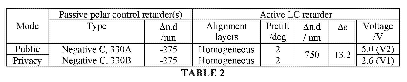
[189] The passive polar control retarder 330 comprises first and second C-plates 330A, 330B; and the switchable liquid crystal layer 314 is provided between the first and second C-plates 330A, 330B. The switchable liquid crystal retarder 301 comprises two surface alignment layers 418A, 418B disposed adjacent to the layer 314 of non-curable liquid crystal material 414 and on opposite sides thereof and each arranged to provide homogeneous alignment in the adjacent non-curable liquid crystal material 414. The layer of non-curable liquid crystal material 414 of the switchable liquid crystal retarder 301 comprises a non-curable liquid crystal material 414 with a positive dielectric anisotropy.
[190] In the present embodiments, desirable ranges for retardations and voltages have been established by means of simulation of retarder stacks and experiment with display optical stacks. Ranges for retardances will now be described that provide design configurations for various optical layers.
[191] The layer of liquid crystal material 314 has a retardance for light of a wavelength of 550nm in a range from 500nm to 1000nm, preferably in a range from 600nm to 900nm and most preferably in a range from 700nm to 850nm. The two passive retarders 330A, 330B each comprises a passive retarder having an optical axis perpendicular to the plane of the retarder and the total retardance of the two passive retarders for light of a wavelength of 550nm is in a range from -300nm to -700nm, preferably in a range from -350mn to -600nm and most preferably in a range from -400nm to -500nm.
[192] Advantageously high optical performance can be achieved in privacy and public modes of operation in very low thickness embodiments.
[193] The operation of privacy displays will now be described further.
[194] FIGURE 8A is a schematic diagram illustrating in front perspective view observation of reflected ambient light from interface surfaces of a display of FIGURE 1A operating in public mode.
[195] Display 100 may be provided with white regions 603 and black regions 601. A snooper 47 may observe an image on the display if luminance difference between the observed regions 601, 603 can be perceived. In operation, primary user 45 observes a full luminance images by rays 700 to viewing locations 26 that may be optical windows of a directional display. Snooper 47 observes reduced luminance rays 402 in viewing locations 27 that may for example be optical windows of a directional display comprising an imaging waveguide. Regions 26, 27 further represent on-axis and
off-axis regions of polar graphs of FIGURES 3C-D.
[196] Thus some light rays 404 may be reflected by the front surface of the additional polariser 318 and other surfaces of the display. Typically, such reflectivity may be 4% for a bonded optical stack at normal incidence and approximately 5% for a bonded optical stack for 45 degrees incidence, due to Fresnel reflections at the air-polariser interface. Thus a low luminance reflected image 605 of source 604 may be observed by the snooper on the front of the display 100.
[197] FIGURE 8B is a schematic diagram illustrating in front perspective view observation of reflected ambient light for the display of FIGURE 1A operating in privacy mode. Regions 26, 27 further represent on-axis and off-axis regions of polar graphs of FIGURES 3A-B. By way of comparison with FIGURE 8 A, substantially higher reflected luminance is observable from reflection 606 of source 604 for the off-axis snooper 47 in off-axis location 27. By comparison, user 45 in location 26 sees a low reflectivity image with high luminance. The shape and distribution of the reflected image 606 is determined by the ambient light source 604 spatial distribution but may be further determined by diffusion layers, particularly at the output surface of the additional polariser
318.
[198] Advantageously the image seen by user 45 has high luminance and image visibility and the image seen by snooper 47 has low luminance and high visual security level.
[199] Features of the arrangement of FIGURES 8A-C not discussed in further detail may be assumed to correspond to the features with equivalent reference numerals as discussed above, including any potential variations in the features.
[200] The appearance of artefacts due to applied force applied to liquid crystal layers without the cured liquid crystal material 420 of the present embodiments will now be described.
[201] FIGURE 9A is a photo showing appearance of disclinations 600 in a nematic liquid crystal layer 314 that does not comprise the cured liquid crystal material of the present embodiments during application of pressure by a finger 25; and FIGURE 9B is a photo showing appearance of disclinations 600 in a nematic liquid crystal layer that does not comprise the cured liquid crystal material of the present embodiments shortly after release of pressure and before complete annealing of the disclinations.
[202] Such disclinations provide undesirable image artefacts over relatively large areas and that last several seconds, and are unacceptable for display appearance.
[203] It would be desirable to provide increased uniformity of public mode of operation
[204] FIGURE 10A is a schematic diagram illustrating in perspective side view an arrangement of a switchable compensated retarder 300 comprising a homeotropically aligned switchable liquid crystal retarder 301 and a negative C-plate 330 in a privacy mode of operation; and FIGURE 10B is a schematic diagram illustrating a graph of liquid crystal director angle against fractional location
through the switchable liquid crystal retarder cell of FIGURE 10A for no applied voltage to provide operation in a public mode of operation.
[205] The substrate 316 may be provided by the retarder 330 to advantageously reduce thickness while the substrate 312 may be provided by a stiffer substrate material such as glass to increase rigidity and advantageously reduce the visibility of artefacts arising from applied force during touch operation.
[206] The switchable liquid crystal retarder 301 comprises two surface alignment layers 418A, 418B disposed adjacent to the non-curable liquid crystal material 414 on opposite sides thereof and arranged to provide homeotropic alignment at the adjacent non-curable liquid crystal material 414. The non-curable liquid crystal material 414 may be provided with a pretilt, for example 88 degrees from the horizontal to remove degeneracy of non-curable liquid crystal material 414 alignment. The cured liquid crystal material 420 may have the same alignment as for the non-curable liquid crystal material 420 when driven with the privacy mode voltage VI. Thus in the public mode the alignment of the materials 414, 420 is different and advantageously some scatter may be provided to increase uniformity.
[207] FIGURE 11A is a schematic graph illustrating the variation of output luminance with polar direction for transmitted light rays in FIGURE 10A in a privacy mode of operation; FIGURE 11B is a schematic graph illustrating the variation in reflectivity with polar direction for reflected light rays in FIGURE 10A in a privacy mode of operation; FIGURE 11C is a schematic graph illustrating the variation of output luminance with polar direction for transmitted light rays in FIGURE 10B in a public mode of operation; and FIGURE 11D is a schematic graph illustrating the variation in reflectivity with polar direction for reflected light rays in FIGURE 10B in a public mode of operation comprising the arrangement described in TABLE 3.

[208] In comparison to the embodiments of TABLES 1 and 2, the liquid crystal retarder alignment is provided by a homeotropic rather than homogeneous alignment Advantageously the wide angle mode performance of FIGURES 11C-D is improved with respect to FIGURES 3C-D. Further the power consumption of the public mode is reduced because of the low drive voltage.
[209] The layer of liquid crystal material of the switchable liquid crystal retarder comprises a liquid crystal material with a negative dielectric anisotropy.
[210] The switchable liquid crystal retarder 301 comprises two surface alignment layers 418A, 418B disposed adjacent to the nan-curable liquid crystal material 414 on opposite sides thereof and each arranged to provide homeotropic alignment at the adjacent non-curable liquid crystal material
414.
[211] In the present embodiments, desirable ranges for retardations and voltages have been established by means of simulation of retarder stacks and experiment with display optical stacks. Ranges for retardances will now be described that provide design configurations for various optical layers.
[212] The layer of liquid crystal material has a retardance for light of a wavelength of 550nm in a range from 500mn to 1000nm, preferably in a range from 600nm to 900nm and most preferably in a range from 700nm to 850nm
[213] The at least one passive retarder comprises a passive retarder having an optical axis perpendicular to the plane of the retarder, the passive retarder having a retardance for light of a wavelength of 550nm in a range from -300nm to -900nm, preferably in a range from -450nm to - 800nm and most preferably in a range from -500nm to -725nm; or (not shown) the at least one passive retarder comprises a pair of passive retarders which have optical axes in the plane of the retarders that are crossed, each passive retarder of the pair of passive retarders having a retardance for light of a wavelength of 550nm in a range from 300nm to 800nm, preferably in a range from 500nm to 700nm and most preferably in a range from 550nm to 675nm
[214] The switchable liquid crystal retarder 301 comprises two surface alignment layers disposed on electrodes 413, 415 and adjacent to the layer of non-curable liquid crystal material 414 and on opposite sides thereof and each arranged to provide homeotropic alignment in the adjacent non- curable liquid crystal material 414. The layer of non-curable liquid crystal material 414 of the switchable liquid crystal retarder 301 comprises a liquid crystal material with a negative dielectric anisotropy. The liquid crystal molecules 414 may be provided with a pretilt, for example 88 degrees from the horizontal to remove degeneracy in switching.
[215] FIGURE 1 1E is a schematic diagram illustrating a graph of liquid crystal director angle 407 against fractional location 440 through the switchable liquid crystal retarder cell, where the fractional location 440 varies between 0 for a location at the surface alignment layer 409 and 1 for a location at the surface alignment layer 411. FIGURE 1 IE differs from FIGURE 4 as the pretilt angle is large and reduces with applied voltage.
[216] For a homeotropically aligned mode with no voltage applied as illustrated in FIGURE 6A, the liquid crystal directors are at a tilt 407 of 88 degrees through the thickness of the cell as indicated by tilt profile 442. The tilt profile for the layer 314 may be the same as the profile 442. The compensation retarder 330 may provide correction for the pretilt direction of the switchable liquid crystal retarder 301. The compensation retarder 330 may alternatively have a uniform tilt angle of 90
degrees, such difference from the pretilt of the liquid crystal layer providing only small difference in off-axis viewing properties. The non-curable liquid crystal material 414 switches between profiles 442 in public mode and 444 in privacy mode while the cured liquid crystal material 420 maintains the profile 444 in both modes of operation.
[217] A method to form the switchable liquid crystal layer of FIGURES 10A-B will now be described.
[218] FIGURES 12A-D are schematic diagrams illustrating in a perspective side view a method to provide a liquid crystal polymer stabilised switchable liquid crystal retarder for a privacy display comprising homeotropic alignment layers. The method of FIGURES 12A-D is similar to that of FIGURES 5A-D other than the liquid crystal materials 414, 420 comprise negative dielectric anisotropy materials and homeotropic alignment layers 418A, 418B are provided.
[219] A method to manufacture a liquid crystal retarder for a privacy display device 100 comprises the steps of: (i) providing first and second transparent support substrates 312, 316 with electrodes 413, 415 on at least one side of each of the first and second transparent support substrates 312, 316; (ii) forming a liquid crystal alignment layer on an electrode 413, 415 of each of the first and second transparent support substrates 312, 316; (iii) providing a liquid crystal layer 314 between the alignment layers; wherein the liquid crystal layer 314 comprises (a) a non-curable liquid crystal material 414 and (b) a cured liquid crystal material 420; and the liquid crystal layer 314 has a retardance for light of a wavelength of 550nm in a range from 500nm to 1000nm, preferably in a range from 600nm to 900nm and most preferably in a range from 700nm to 850nm; (iv) applying a curing step voltage across the electrodes; and (v) curing the curable liquid crystal material 420. The curing step voltage VI is the voltage at which the liquid crystal retarder is driven to provide a privacy mode of operation of the display device (such as illustrated in FIGURE 2A). The curable liquid crystal material 420 comprises a photo-initiator and the step of curing the curable liquid crystal material comprises illumination by ultraviolet radiation 720.
[220] In further detail, as illustrated in FIGURE 12A, in a first step a liquid crystal layer is provided, wherein the liquid crystal material comprises non-curable liquid crystal molecules 414 and curable liquid crystal molecules 420. Alignment layers (not shown) are arranged to provide alignment, such as homogeneous alignment at each surface by means of anti-parallel pre-tilt alignments.
[221] As illustrated in FIGURE 12B, a voltage may be applied across the liquid crystal layer 413 by means of electrodes 413, 415. The voltage may be substantially the same voltage VI provided to achieve the liquid crystal alignment state for privacy operation.
[222] As illustrated in FIGURE 12C, the cell may be cured while the voltage remains applied. Curable liquid crystal material 420 may comprise for example reactive mesogen molecules, with a similar birefringence to that of the non-curable liquid crystal material 414 and a photo initiator.
[223] As illustrated in FIGURE 12D, after cure the light source 722 and voltage driver are removed and the molecules of the non-curable liquid crystal material 414 relax while the molecules of the cured liquid crystal material 420 remain in the cured liquid crystal network 424 comprising the molecular orientation of the driven state.
[224] The operation of polar control retarder layers between parallel polarisers for off-axis illumination will now be described further. In the various devices described above, at least one polar control retarder is arranged between the reflective polariser 318 and the additional polariser 218 in various different configurations. In each case, the at least one polar control retarder is configured so that it does not affect the luminance of light passing through the reflective polariser 318, the at least one polar control retarder, and the additional polariser 218 along an axis along a normal to the plane of the polar control retarder(s) but it does reduce the luminance of light passing through the reflective polariser 318, the at least one polar control retarder, and the additional polariser 218 along an axis inclined to a normal to the plane of the polar control retarder(s), at least in one of the switchable states of the compensated switchable polar control polar control retarder 300. There will now be given a description of this effect in more detail, the principles of which may be applied in general to all of the devices described above.
[225] FIGURE 13A is a schematic diagram illustrating in perspective view illumination of a polar control retarder layer by off-axis light. Polar control retarder 630 may comprise birefnngent material, represented by refractive index ellipsoid 632 with optical axis direction 634 at 0 degrees to the x-axis, and have a thickness 631. Features of the arrangements of FIGURES 13A-15E below that are not discussed in further detail may be assumed to correspond to the features with equivalent reference numerals as discussed above, including any potential variations in the features.
[226] Normal light rays 636 propagate so that the path length in the material is the same as the thickness 631. Light rays 637 are in the y-z plane have an increased path length; however the birefringence of the material is substantially the same as the rays 636. By way of comparison fight rays 638 that are in the x-z plane have an increased path length in the birefnngent material and further the birefringence is different to the normal ray 636.
[227] The retardance of the polar control retarder 630 is thus dependent on the angle of incidence of the respective ray, and also the plane of incidence, that is rays 638 in the x-z will have a retardance different from the normal rays 636 and the rays 637 in the y-z plane.
[228] The interaction of polarized fight with the polar control retarder 630 will now be described. To distinguish from the first and second polarization components during operation in a directional backlight 101, the following explanation will refer to third and fourth polarization components.
[229] FIGURE 13B is a schematic diagram illustrating in perspective view illumination of a polar control retarder layer by off-axis fight of a third linear polarization state at 90 degrees to the x-axis and FIGURE 13C is a schematic diagram illustrating in perspective view illumination of a polar
control retarder layer by off-axis light of a fourth linear polarization state at 0 degrees to the x-axis. In such arrangements, the incident linear polarization states are aligned to the optical axes of the birefringent material, represented by ellipse 632. Consequently, no phase difference between the third and fourth orthogonal polarization components is provided, and there is no resultant change of the polarization state of the linearly polarized input for each ray 636, 637, 638. Thus, the polar control retarder 630 introduces no phase shift to polarisation components of light passed by the polariser on the input side of the polar control retarder 630 along an axis along a normal to the plane of the polar control retarder 630. Accordingly, the polar control retarder 630 does not affect the luminance of light passing through the polar control retarder 630 and polatisers (not shown) on each side of the polar control retarder 630. Although FIGURES 29A-C relate specifically to the polar control retarder 630 that is passive, a similar effect is achieved by the polar control retarders in the devices described above.
[230] FIGURE 13D is a schematic diagram illustrating in perspective view illumination of a polar control retarder 630 layer by off-axis light of a linear polarization state at 45 degrees. The linear polarization state may be resolved into third and fourth polarization components that are respectively orthogonal and parallel to optical axis 634 direction The polar control retarder thickness 631 and material retardance represented by refractive index ellipsoid 632 may provide a net effect of relatively shifting the phase of the third and fourth polarization components incident thereon in a normal direction represented by ray 636 by half a wavelength, for a design wavelength The design wavelength may for example be in the range of 500 to 550 nm.
[231] At the design wavelength and for light propagating normally along ray 636 then the output polarization may be rotated by 90 degrees to a linear polarization state 640 at -45 degrees. Light propagating along ray 637 may see a phase difference that is similar but not identical to the phase difference along ray 637 due to the change in thickness, and thus an elliptical polarization state 639 may be output which may have a major axis similar to the linear polarization axis of the output light for ray 636.
[232] By way of contrast, the phase difference for the incident linear polarization state along ray 638 may be significantly different, in particular a lower phase difference may be provided. Such phase difference may provide an output polarization state 644 that is substantially circular at a given inclination angle 642. Thus, the polar control retarder 630 introduces a phase shift to polarisation components of light passed by the polariser on the input side of the polar control retarder 630 along an axis corresponding to ray 638 that is inclined to a normal to the plane of the polar control retarder 630. Although FIGURE 29D relates to the polar control retarder 630 that is passive, a similar effect is achieved by the polar control retarders described above, in a switchable state of the switchable liquid crystal polar control retarder corresponding to the privacy mode.
[233] To illustrate the off-axis behaviour of polar control retarder stacks, the angular luminance control of C-plates 330A, 330B between an additional polariser 318 and output display polariser 218 will now be described for various off-axis illumination arrangements with reference to the operation of a C-plate between the parallel polarisers 500, 210 will now be described.
[234] FIGURE 14A is a schematic diagram illustrating in perspective view illumination of a C- plate layer by off-axis polarised light with a positive elevation Incident linear polarisation component 704 is incident onto the birefringent material 632 of the polar control retarder 560 that is a C-plate with optical axis direction 507 that is perpendicular to the plane of the polar control retarder 560. Polarisation component 704 sees no net phase difference on transmission through the liquid crystal molecule and so the output polarisation component is the same as component 704. Thus a maximum transmission is seen through the polariser 210. Thus the polar control retarder 560 having an optical axis 561 perpendicular to the plane of the polar control retarder 560, that is the x-y plane. The polar control retarder 560 having an optical axis perpendicular to the plane of the polar control retarder comprises a C-plate.
[235] FIGURE 14B is a schematic diagram illustrating in perspective view illumination of a C- plate layer by off-axis polarised light with a negative lateral angle. As with the arrangement of FIGURE 14A, polarisation state 704 sees no net phase difference and is transmitted with maximum luminance. Thus, the polar control retarder 560 introduces no phase shift to polarisation components of light passed by the polariser on the input side of the polar control retarder 560 along an axis along a normal to the plane of the polar control retarder 560. Accordingly, the polar control retarder 560 does not affect the luminance of light passing through the polar control retarder 560 and polarisers (not shown) on each side of the polar control retarder 560. Although FIGURES 29A-C relate specifically to the polar control retarder 560 that is passive, a similar effect is achieved by the polar control retarders in the devices described above.
[236] FIGURE 14C is a schematic diagram illustrating in perspective view illumination of a C- plate layer by off-axis polarised light with a positive elevation and negative lateral angle. In comparison to the arrangement of FIGURES 14A-B, the polarisation state 704 resolves onto eigenstates 703, 705 with respect to the birefringent material 632 providing a net phase difference on transmission through the polar control retarder 560. The resultant elliptical polarisation component 656 is transmitted through polariser 210 with reduced luminance in comparison to the rays illustrated in FIGURES 14A-B.
[237] FIGURE 14D is a schematic diagram illustrating in perspective view illumination of a C- plate layer by off-axis polarised light with a positive elevation and positive lateral angle. In a similar manner to FIGURE 14C, the polarisation component 704 is resolved into eigenstates 703, 705 that undergo a net phase difference, and elliptical polarisation component 660 is provided, which after transmission through the polariser reduces the luminance of the respective off-axis ray. Thus, the
polar control retarder 560 introduces a phase shift to polarisation components of light passed by the polariser on the input side of the polar control retarder 560 along an axis that is inclined to a normal to the plane of the polar control retarder 560. Although FIGURE 29D relates to the polar control retarder 560 that is passive, a similar effect is achieved by the polar control retarders described above, in a switchable state of the switchable liquid crystal polar control retarder corresponding to the privacy mode.
[238] FIGURE 14E is a schematic graph illustrating the variation of output transmission with polar direction for transmitted light rays in FIGURES 14A-D. Thus, the C-plate may provide luminance reduction in polar quadrants. In combination with switchable liquid crystal layer 314 described elsewhere herein, (i) removal of luminance reduction of the C-plate may be provided in a first wide angle state of operation (ii) extended polar region for luminance reduction may be achieved in a second privacy state of operation.
[239J To illustrate the off-axis behaviour of polar control retarder stacks, the angular luminance control of crossed A-plates 330A, 330B between an additional polariser 318 and output display polariser 218 will now be described for various off-axis illumination arrangements.
[240] FIGURE 15A is a schematic diagram illustrating in perspective view illumination of crossed A-plate retarder layers by off-axis polarised light with a positive elevation Linear polariser 218 with electric vector transmission direction 219 is used to provide a linear polarisation state 704 that is parallel to the lateral direction onto first A-plate 330A of the crossed A-plates 330A, 330B. The optical axis direction 331A is inclined at +45 degrees to the lateral direction The retardance of the polar control retarder 330A for the off-axis angle q1 in the positive elevation direction provides a resultant polarisation component 650 that is generally elliptical on output. Polarisation component 650 is incident onto the second A-plate 330B of the crossed A-plates 330A, 330B that has an optical axis direction 33 IB that is orthogonal to the optical axis direction 331 A of the first A-plate 330A. In the plane of incidence of FIGURE 15A, the retardance of the second A-plate 330B for the off-axis angle q1 is equal and opposite to the retardance of the first A-plate 330A. Thus a net zero retardation is provided for the incident polarisation component 704 and the output polarisation component is the same as the input polarisation component 704.
[241] The output polarisation component is aligned to the electric vector transmission direction of the additional polariser 318, and thus is transmitted efficiently. Advantageously substantially no losses are provided for light rays that have zero lateral angle angular component so that full transmission efficiency is achieved.
[242] FIGURE 15B is a schematic diagram illustrating in perspective view illumination of crossed A-plate retarder layers by off-axis polarised light with a negative lateral angle. Thus input polarisation component is converted by the first A-plate 330A to an intermediate polarisation component 652 that is generally an elliptical polarisation state. The second A-plate 330B again
provides an equal and opposite retardation to the first A-plate so that the output polarisation component is the same as the input polarisation component 704 and light is efficiently transmitted through the polariser 318.
[243] Thus the polar control retarder comprises a pair of retarders 330A, 330B which have optical axes in the plane of the retarders 330A, 330B that are crossed, that is the x-y plane in the present embodiments. The pair of retarders 330A, 330B have optical axes 331 A, 33 IB that each extend at 45° with respect to an electric vector transmission direction that is parallel to the electric vector transmission of the polariser 318.
[244] Advantageously substantially no losses are provided for light rays that have zero elevation angular component so that full transmission efficiency is achieved.
[245] FIGURE 15C is a schematic diagram illustrating in perspective view illumination of crossed A-plate retarder layers by off-axis polarised light with a positive elevation and negative lateral angle. Polarisation component 704 is converted to an elliptical polarisation component 654 by first A-plate 330A. A resultant elliptical component 656 is output from the second A-plate 330B. Elliptical component 656 is analysed by input polariser 318 with reduced luminance in comparison to the input luminance of the first polarisation component 704.
[246] FIGURE 15D is a schematic diagram illustrating in perspective view illumination of crossed A-plate retarder layers by off-axis polarised light with a positive elevation and positive lateral angle. Polarisation components 658 and 660 are provided by first and second A-plates 330A, 330B as net retardance of first and second retarders does not provide compensation.
[247] Thus luminance is reduced for light rays that have non-zero lateral angle and non-zero elevation components. Advantageously display privacy can be increased for snoopers that are arranged in viewing quadrants while luminous efficiency for primary display users is not substantially reduced.
[248] FIGURE 15E is a schematic graph illustrating the variation of output transmission with polar direction for transmitted light rays in FIGURES 15A-D. In comparison to the arrangement of FIGURE 14E, the area of luminance reduction is increased for off-axis viewing. However, the switchable liquid crystal layer 314 may provide reduced uniformity in comparison to the C-plate arrangements for off-axis viewing in the first public mode state of operation
[249] As may be used herein, the terms“substantially” and“approximately” provide an industry- accepted tolerance for its corresponding term and/or relativity between items. Such an industry- accepted tolerance ranges from zero percent to ten percent and corresponds to, but is not limited to, component values, angles, et cetera. Such relativity between items ranges between approximately zero percent to ten percent
[250] While various embodiments in accordance with the principles disclosed herein have been described above, it should be understood that they have been presented by way of example only, and
not limitation Thus, the breadth and scope of this disclosure should not be limited by any of the above-described exemplary embodiments, but should be defined only in accordance with any claims and their equivalents issuing from this disclosure. Furthermore, the above advantages and features are provided in described embodiments, but shall not limit the application of such issued claims to processes and structures accomplishing any or all of the above advantages.
[251] Additionally, the section headings herein are provided for consistency with the suggestions under 37 CFR 1.77 or otherwise to provide organizational cues. These headings shall not limit or characterize the embodiment(s) set out in any claims that may issue from this disclosure. Specifically and by way of example, although the headings refer to a“Technical Field,” the claims should not be limited by the language chosen under this heading to describe the so-called field. Further, a description of a technology in the“Background” is not to be construed as an admission that certain technology is prior art to any embodiments) in this disclosure. Neither is the“Summary” to be considered as a characterization of the embodiments) set forth in issued claims. Furthermore, any reference in this disclosure to“invention" in the singular should not be used to argue that there is only a single point of novelty in this disclosure. Multiple embodiments may be set forth according to the limitations of the multiple claims issuing from this disclosure, and such claims accordingly define the embodiment(s), and their equivalents, that are protected thereby. In all instances, the scope of such claims shall be considered on their own merits in light of this disclosure, but should not be constrained by the headings set forth herein.
Claims
1. A display device comprising:
a spatial light modulator,
a display polariser arranged on a side of the spatial light modulator, the display polariser being a linear polariser,
an additional polariser arranged on the same side of the spatial light modulator as the display polariser, the additional polariser being a linear polariser; and
at least one polar control retarder arranged between the additional polariser and the display polariser,
wherein the at least one polar control retarder comprises a switchable liquid crystal retarder comprising:
first and second support substrates;
a liquid crystal layer disposed between the first and second transparent support substrates, the liquid crystal layer comprising non-curable liquid crystal material and cured polymer material; electrodes arranged to apply a voltage for controlling the liquid crystal layer, and respective liquid crystal alignment layers supported on the first and second the support substrates adjacent the liquid crystal layer for aligning the non-curable liquid crystal material.
2. A display device according to claim 1 wherein the cured polymer material comprises an acrylate or a thiol material.
3. A display device according to claim 1 or 2 wherein the cured polymer material comprises a cured liquid crystal material.
4. A display device according to claim 3, wherein the cured liquid crystal material comprises a reactive mesogen
5. A display device according to claim 3 or 4 wherein the cured liquid crystal material has an alignment that is aligned with the alignment of the non-curable liquid crystal material in a state in which a predetermined voltage is applied to the electrodes.
6. A display device according to claim 5, wherein the predetermined voltage is capable of causing the layer of cured liquid crystal material and non-curable liquid crystal material simultaneously to introduce no net relative phase shift to orthogonal polarisation components of tight passed by the display polariser along an axis along a normal to the plane of the at least one polar
control retarder and to introduce a net relative phase shift to orthogonal polarisation components of tight passed by the additional polariser along an axis inclined to a normal to the plane of the at least one polar control retarder.
7. A display device according to any one of the preceding claims wherein the ratio of the volume of the cured polymer material to the volume of the non-curable liquid crystal material is less than 5%.
8. A display device according to any one of the preceding claims, wherein the cured polymer material is arranged in a network that extends between the two support substrates.
9. A display device according to claim 8, wherein the network is attached to each of the two support substrates.
10. A display device according to ary one of the preceding claims, wherein the electrodes are disposed on opposite sides of the liquid crystal layer.
11. A display device according to any one of the preceding claims, further comprising a control system arranged to control the voltage applied to the electrodes of the switchable liquid crystal retarder.
12. A display device according to any one of the preceding claims, wherein the at least one polar control retarder further comprises at least one passive compensation retarder.
13. A display device according to any one of the preceding claims, wherein the switchable liquid crystal retarder comprises two surface alignment layers disposed adjacent to the liquid crystal material on opposite sides thereof and each arranged to provide homeotropic alignment at the adjacent liquid crystal material.
14. A display device according to claim 13, wherein the layer of liquid crystal material of the switchable liquid crystal retarder comprises a liquid crystal material with a negative dielectric anisotropy.
15. A display device according to claim 13 or 14, wherein the layer of liquid crystal material has a relardance for light of a wavelength of 550nm in a range from 500nm to 1000nm, preferably in a range from 600nm to 900mn and most preferably in a range from 700nm to 850nm.
16. A display device according to any one of claims 13 to 15, wherein:
the at least one passive retarder comprises at least one passive retarder having an optical axis perpendicular to the plane of the retarder, the at least one passive retarder having a total retardance for light of a wavelength of 550nm in a range from -300nm to -900nm, preferably in a range from - 450nm to -800nm and most preferably in a range from -500nm to -725nm; or
the at least one passive retarder comprises a pair of passive retarders which have optical axes in the plane of the retarders that are crossed, each passive retarder of the pair of passive retarders having a retardance for light of a wavelength of 550nm in a range from 300nm to 500nm, preferably in a range from 500nm to 700nm and most preferably in a range from 550nm to 675nm
17. A display device according to claims 1 to 12, wherein the switchable liquid crystal retarder comprises two surface alignment layers disposed adjacent to the layer of liquid crystal material and on opposite sides thereof and each arranged to provide homogeneous alignment in the adjacent liquid crystal material.
18. A display device according to claim 17, wherein the layer of liquid crystal material of the switchable liquid crystal retarder comprises a liquid crystal material with a positive dielectric anisotropy.
19. A display device according to claim 17 or 18, wherein the layer of liquid crystal material has a retardance for light of a wavelength of 550nm in a range from 500nm to 900nm, preferably in a range from 600nm to 850nm and most preferably in a range from 700nm to 800nm.
20. A display device according to any one of claims 17 to 19, wherein:
the at least one passive retarder comprises at least one passive retarder having an optical axis perpendicular to the plane of the retarder, the at least one passive retarder having a total retardance for light of a wavelength of 550nm in a range from -300nm to -700nm, preferably in a range from - 350nm to -600nm and most preferably in a range from -400nm to - 500nm; or
the at least one passive retarder comprises a pair of passive retarders which have optical axes in the plane of the retarders that are crossed, each passive retarder of the pair of passive retarders having a retardance for light of a wavelength of 550nm in a range from 300nm to 500nm, preferably in a range from 350nm to 650nm and most preferably in a range from 450nm to 550nm.
21. A method of manufacturing a switchable liquid crystal retarder which is a polar control retarder for a display device, the method comprising:
providing first and second support substrates having electrodes for controlling a liquid crystal layer and having first and second liquid crystal alignment layers supported thereon for aligning liquid crystal material of the liquid crystal layer;
disposing a liquid crystal layer disposed between the first and second transparent support substrates with the first and second liquid crystal alignment layers adjacent the liquid crystal layer, the liquid crystal layer comprising non-curable liquid crystal material and curable liquid crystal material; and
curing the curable liquid crystal material while applying a predetermined voltage to the electrodes.
22. A method according to claim 21, wherein the predetermined voltage is capable of causing layer of cured liquid crystal material and the non-curable liquid crystal material simultaneously to introduce no net relative phase shift to orthogonal polarisation components of light passed by the additional polariser along an axis along a normal to the plane of the at least one polar control retarder and to introduce a net relative phase shift to orthogonal polarisation components of light passed by the additional polariser along an axis inclined to a normal to the plane of the at least one polar control retarder.
23. A method according to claim 21 or 22, wherein the curable liquid crystal material is a reactive mesogen
24. A method according to any one of claims 21 to 23, wherein
the liquid crystal layer further comprises a polymerisation photo-initiator, and
the step of curing the curable liquid crystal material is performed by applying light radiation, and preferably ultraviolet light radiation to the liquid crystal layer.
25. A method according to any one of claims 21 to 24 wherein the predetermined voltage is nonzero.
Priority Applications (2)
| Application Number | Priority Date | Filing Date | Title |
|---|---|---|---|
| CN201980056022.0A CN112639591B (en) | 2018-06-29 | 2019-06-21 | Stabilization of privacy display |
| EP19825448.4A EP3814832B1 (en) | 2018-06-29 | 2019-06-21 | Stabilization for privacy display |
Applications Claiming Priority (6)
| Application Number | Priority Date | Filing Date | Title |
|---|---|---|---|
| US201862691896P | 2018-06-29 | 2018-06-29 | |
| US62/691,896 | 2018-06-29 | ||
| US201962789322P | 2019-01-07 | 2019-01-07 | |
| US62/789,322 | 2019-01-07 | ||
| US201962796423P | 2019-01-24 | 2019-01-24 | |
| US62/796,423 | 2019-01-24 |
Publications (1)
| Publication Number | Publication Date |
|---|---|
| WO2020005756A1 true WO2020005756A1 (en) | 2020-01-02 |
Family
ID=68985151
Family Applications (2)
| Application Number | Title | Priority Date | Filing Date |
|---|---|---|---|
| PCT/US2019/038466 Ceased WO2020005756A1 (en) | 2018-06-29 | 2019-06-21 | Stabilization for privacy display |
| PCT/US2019/038409 Ceased WO2020005748A1 (en) | 2018-06-29 | 2019-06-21 | Optical stack for privacy display |
Family Applications After (1)
| Application Number | Title | Priority Date | Filing Date |
|---|---|---|---|
| PCT/US2019/038409 Ceased WO2020005748A1 (en) | 2018-06-29 | 2019-06-21 | Optical stack for privacy display |
Country Status (4)
| Country | Link |
|---|---|
| US (5) | US10955715B2 (en) |
| EP (2) | EP3814832B1 (en) |
| CN (2) | CN112639592B (en) |
| WO (2) | WO2020005756A1 (en) |
Families Citing this family (39)
| Publication number | Priority date | Publication date | Assignee | Title |
|---|---|---|---|---|
| PL2604286T3 (en) | 2003-05-01 | 2015-03-31 | Cornell Res Foundation Inc | Method and Carrier Complexes for Delivering Molecules to Cells |
| US11079619B2 (en) | 2016-05-19 | 2021-08-03 | Reald Spark, Llc | Wide angle imaging directional backlights |
| CN110809732B (en) | 2017-05-08 | 2025-01-10 | 瑞尔D斯帕克有限责任公司 | Optical stack for imaging directional backlights |
| JP7237018B2 (en) * | 2017-06-06 | 2023-03-10 | スリーエム イノベイティブ プロパティズ カンパニー | Backlight comprising a wide web turning film and a reflective polarizer with a quarter wave retarder |
| TWI878209B (en) | 2017-09-15 | 2025-04-01 | 美商瑞爾D斯帕克有限責任公司 | Display device and a view angle control optical element for application to a display device |
| EP3743766B1 (en) | 2018-01-25 | 2026-02-11 | RealD Spark, LLC | Touch screen for privacy display |
| CN115718382A (en) | 2018-01-25 | 2023-02-28 | 瑞尔D斯帕克有限责任公司 | Reflective optical stack for privacy display device |
| US10935714B2 (en) | 2018-03-22 | 2021-03-02 | Reald Spark, Llc | Optical waveguide for directional backlight |
| US10955715B2 (en) | 2018-06-29 | 2021-03-23 | Reald Spark, Llc | Optical stack for privacy display |
| US11073735B2 (en) | 2018-07-18 | 2021-07-27 | Reald Spark, Llc | Optical stack for switchable directional display |
| WO2020072643A1 (en) | 2018-10-03 | 2020-04-09 | Reald Spark, Llc | Privacy display control apparatus |
| CN113167953B (en) | 2018-11-07 | 2023-10-24 | 瑞尔D斯帕克有限责任公司 | Directional display device |
| US11287677B2 (en) | 2019-01-07 | 2022-03-29 | Reald Spark, Llc | Optical stack for privacy display |
| US11029566B2 (en) * | 2019-02-12 | 2021-06-08 | Reald Spark, Llc | Diffuser for privacy display |
| TWI912252B (en) | 2019-07-02 | 2026-01-21 | 美商瑞爾D斯帕克有限責任公司 | Directional display apparatus |
| CN114846393B (en) | 2019-11-13 | 2024-12-03 | 瑞尔D斯帕克有限责任公司 | Off-axis display device |
| WO2021102148A1 (en) * | 2019-11-22 | 2021-05-27 | Valve Corporation | Head-mounted display (hmd) with spatially-varying retarder optics |
| WO2021118936A1 (en) | 2019-12-10 | 2021-06-17 | Reald Spark, Llc | Control of reflections of a display device |
| WO2021222615A1 (en) | 2020-04-30 | 2021-11-04 | Reald Spark, Llc | Directional display apparatus |
| WO2021222598A1 (en) | 2020-04-30 | 2021-11-04 | Reald Spark, Llc | Directional display apparatus |
| DE102020113714A1 (en) | 2020-05-20 | 2021-11-25 | Bayerische Motoren Werke Aktiengesellschaft | Display device for automobiles |
| TWI898003B (en) | 2020-07-29 | 2025-09-21 | 美商瑞爾D斯帕克有限責任公司 | Pupillated illumination apparatus |
| EP4189285A4 (en) | 2020-07-29 | 2024-07-24 | RealD Spark, LLC | REAR LIGHTING FOR A SWITCHABLE DIRECTION INDICATOR |
| CN112034640B (en) | 2020-09-11 | 2023-03-17 | 京东方科技集团股份有限公司 | Peep-proof panel, preparation method, driving method and display device |
| US11906828B2 (en) | 2020-09-30 | 2024-02-20 | Sioptica Gmbh | Switchable light filter and use thereof |
| KR102874923B1 (en) * | 2021-01-12 | 2025-10-24 | 삼성디스플레이 주식회사 | Display device |
| US11892717B2 (en) | 2021-09-30 | 2024-02-06 | Reald Spark, Llc | Marks for privacy display |
| CN114089552A (en) * | 2021-11-18 | 2022-02-25 | 武汉华星光电技术有限公司 | Display panel and display device |
| TW202332973A (en) | 2022-02-09 | 2023-08-16 | 美商瑞爾D斯帕克有限責任公司 | Display device with uniform off-axis luminance reduction |
| US11977286B2 (en) | 2022-02-09 | 2024-05-07 | Reald Spark, Llc | Observer-tracked privacy display |
| US11892718B2 (en) | 2022-04-07 | 2024-02-06 | Reald Spark, Llc | Directional display apparatus |
| CN115728978B (en) * | 2022-04-18 | 2026-02-17 | 友达光电股份有限公司 | Display device and manufacturing method thereof |
| NL2032216B1 (en) * | 2022-06-17 | 2024-01-05 | Dimenco Holding B V | Method for reducing disclinations in a 2d/3d switchable autostereoscopic display |
| KR20240053723A (en) | 2022-10-17 | 2024-04-25 | 삼성디스플레이 주식회사 | Pixel and display device including same |
| CN218675579U (en) * | 2022-12-07 | 2023-03-21 | 中强光电股份有限公司 | display device |
| TW202441227A (en) * | 2023-03-29 | 2024-10-16 | 美商瑞爾D斯帕克有限責任公司 | Marks for angular optical filters |
| DE102023110269B3 (en) | 2023-04-21 | 2023-12-28 | Sioptica Gmbh | Switchable light filter, lighting device and screen |
| US12523899B2 (en) | 2023-04-25 | 2026-01-13 | Reald Spark, Llc | Switchable privacy display |
| WO2025030030A2 (en) | 2023-08-03 | 2025-02-06 | Reald Spark, Llc | Privacy displays |
Citations (10)
| Publication number | Priority date | Publication date | Assignee | Title |
|---|---|---|---|---|
| US5894361A (en) * | 1995-10-15 | 1999-04-13 | Semiconductor Energy Laboratory Co., Ltd. | Stereoscopic liquid crystal display having different orientation domains |
| US20060082702A1 (en) * | 2002-06-28 | 2006-04-20 | Jacobs Adrian M S | Optical device and display operating in two dimensional and autostereoscopic three dimensional modes |
| US8237876B2 (en) | 2005-05-25 | 2012-08-07 | Kim Leong Tan | Tilted C-plate retarder compensator and display systems incorporating the same |
| WO2016195786A1 (en) | 2015-06-03 | 2016-12-08 | Apple Inc | Electronic device display with switchable film structures |
| US20170031206A1 (en) * | 2015-07-29 | 2017-02-02 | Sharp Kabushiki Kaisha | Sunlight readable lcd with uniform in-cell retarder |
| US20180321553A1 (en) | 2017-05-08 | 2018-11-08 | Reald Spark, Llc | Optical stack for directional display |
| US10126575B1 (en) | 2017-05-08 | 2018-11-13 | Reald Spark, Llc | Optical stack for privacy display |
| US20190086706A1 (en) | 2017-09-15 | 2019-03-21 | Reald Spark, Llc | Optical stack for switchable directional display |
| US10303030B2 (en) | 2017-05-08 | 2019-05-28 | Reald Spark, Llc | Reflective optical stack for privacy display |
| KR101990286B1 (en) * | 2015-12-18 | 2019-06-18 | 주식회사 엘지화학 | Vertical Alignment Layer |
Family Cites Families (372)
| Publication number | Priority date | Publication date | Assignee | Title |
|---|---|---|---|---|
| US3914022A (en) | 1974-07-02 | 1975-10-21 | Gen Electric | Quasi-homeotropic twisted nematic liquid crystal device |
| US4059916A (en) | 1975-01-30 | 1977-11-29 | Copal Company Limited | Light diffusing device |
| JPS58143305A (en) | 1982-02-22 | 1983-08-25 | Hitachi Ltd | Display panel |
| US4621898A (en) | 1983-03-17 | 1986-11-11 | Allied Corporation | Directional optical filter |
| CA1312320C (en) | 1987-11-12 | 1993-01-05 | Makoto Oe | Plane light source unit |
| JPH06142Y2 (en) | 1988-02-29 | 1994-01-05 | 株式会社三洋物産 | Pachinko machine game board |
| US5005108A (en) | 1989-02-10 | 1991-04-02 | Lumitex, Inc. | Thin panel illuminator |
| US4974941A (en) | 1989-03-08 | 1990-12-04 | Hercules Incorporated | Process of aligning and realigning liquid crystal media |
| AU628953B2 (en) | 1989-04-03 | 1992-09-24 | Canon Kabushiki Kaisha | Liquid crystal apparatus |
| GB9017938D0 (en) | 1990-08-15 | 1990-09-26 | Taylor Made Energy Savers Limi | Thermal insulation |
| US5671994A (en) | 1994-06-08 | 1997-09-30 | Clio Technologies, Inc. | Flat and transparent front-lighting system using microprisms |
| DE19521254A1 (en) | 1994-06-24 | 1996-01-04 | Minnesota Mining & Mfg | Display system with brightness boosting film |
| US5835166A (en) | 1994-08-17 | 1998-11-10 | Hall; Dennis R. | Chiral nematic liquid crystal polarization modulated color display for stereoscopic viewing device |
| US5808784A (en) | 1994-09-06 | 1998-09-15 | Dai Nippon Printing Co., Ltd. | Lens array sheet surface light source, and transmission type display device |
| US6380997B1 (en) | 1995-04-07 | 2002-04-30 | Colorlink, Inc. | Achromatic polarization inverters for displaying inverse frames in DC balanced liquid crystal displays |
| US5658490A (en) * | 1995-04-07 | 1997-08-19 | Board Of Regents Of The University Of Colorado | Liquid crystal achromatic compound retarder |
| CA2220519A1 (en) | 1995-05-09 | 1996-11-21 | James P. Coleman | Conductive font |
| US5579139A (en) | 1995-06-07 | 1996-11-26 | Ois Optical Imaging Systems, Inc. | LCD with reduced canopy reflection having a retarder of 220-320 nm retardation outside a polarizer |
| TW331593B (en) | 1996-05-13 | 1998-05-11 | Konika Co Ltd | Planer light source device and light guide plate |
| US5914760A (en) | 1996-06-21 | 1999-06-22 | Casio Computer Co., Ltd. | Surface light source device and liquid crystal display device using the same |
| GB2314640A (en) | 1996-06-26 | 1998-01-07 | Sharp Kk | Liquid crystal devices |
| US6046849A (en) | 1996-09-12 | 2000-04-04 | Sharp Kabushiki Kaisha | Parallax barrier, display, passive polarisation modulating optical element and method of making such an element |
| US6642981B1 (en) | 1996-09-30 | 2003-11-04 | Fujitsu Display Technologies Corporation | Liquid crystal display device operating in a vertically aligned mode including at least one retardation film |
| US5854872A (en) | 1996-10-08 | 1998-12-29 | Clio Technologies, Inc. | Divergent angle rotator system and method for collimating light beams |
| GB2318878A (en) * | 1996-10-31 | 1998-05-06 | Sharp Kk | Reflective liquid crystal device |
| CA2222313C (en) * | 1996-12-12 | 2001-04-03 | Gregory P. Crawford | Liquid crystal display employing dual negative retarders and a brightness enhancing film |
| JPH10268251A (en) | 1997-03-27 | 1998-10-09 | Advanced Display:Kk | Control method for liquid crystal display device |
| US5791757A (en) | 1997-04-01 | 1998-08-11 | Ford Global Technologies, Inc. | Vehicle lighting system utilizing a uniform thickness thin sheet optical element |
| US6280043B1 (en) | 1997-05-14 | 2001-08-28 | Enplas Corporation | Surface light source device of side light type |
| JP3615355B2 (en) | 1997-06-04 | 2005-02-02 | 株式会社エンプラス | Sidelight type surface light source device and light guide plate |
| US6141070A (en) | 1997-06-13 | 2000-10-31 | Citizen Watch Co., Ltd. | Normally black liquid crystal display with twisted compensator and . .DELTAnd of 1500-1800 nm |
| US6055103A (en) | 1997-06-28 | 2000-04-25 | Sharp Kabushiki Kaisha | Passive polarisation modulating optical element and method of making such an element |
| US6099758A (en) | 1997-09-17 | 2000-08-08 | Merck Patent Gesellschaft Mit Beschrankter Haftung | Broadband reflective polarizer |
| US6411306B1 (en) | 1997-11-14 | 2002-06-25 | Eastman Kodak Company | Automatic luminance and contrast adustment for display device |
| GB2331883A (en) | 1997-11-26 | 1999-06-02 | Sharp Kk | Dual image viewing system |
| JP3322197B2 (en) | 1997-12-17 | 2002-09-09 | 松下電器産業株式会社 | Liquid crystal display |
| FI106323B (en) | 1998-12-30 | 2001-01-15 | Nokia Mobile Phones Ltd | The backlight light guide for a flat screen |
| US6392727B1 (en) | 1998-12-31 | 2002-05-21 | Honeywell International Inc. | Reduced reflectance polarized display |
| US6256447B1 (en) | 1998-12-31 | 2001-07-03 | Physical Optics Corporation | Backlight for correcting diagonal line distortion |
| US6752505B2 (en) | 1999-02-23 | 2004-06-22 | Solid State Opto Limited | Light redirecting films and film systems |
| JP2002540557A (en) | 1999-03-24 | 2002-11-26 | エルジー ケミカル エルティーディー. | Backlight system |
| JP3405972B2 (en) | 2000-01-11 | 2003-05-12 | 株式会社東芝 | Liquid crystal display |
| KR20010104725A (en) | 2000-01-14 | 2001-11-26 | 요트.게.아. 롤페즈 | Display device |
| US6347874B1 (en) | 2000-02-16 | 2002-02-19 | 3M Innovative Properties Company | Wedge light extractor with risers |
| WO2001077744A1 (en) | 2000-04-10 | 2001-10-18 | Sony Corporation | Liquid crystal display, liquid crystal display element and liquid crystal display system |
| JP2002050219A (en) | 2000-07-25 | 2002-02-15 | Internatl Business Mach Corp <Ibm> | Planar light source device, light guide plate, display device |
| KR100621495B1 (en) | 2001-02-28 | 2006-09-13 | 가부시키가이샤 히타치 디스프레이즈 | Apparatus which can switch image display state and mirror state, and apparatus having same |
| JP4148657B2 (en) * | 2001-04-04 | 2008-09-10 | シャープ株式会社 | Liquid crystal display |
| GB0114998D0 (en) | 2001-06-20 | 2001-08-08 | Secr Defence | Liquid crystal device |
| KR100799156B1 (en) | 2001-07-13 | 2008-01-29 | 삼성전자주식회사 | Light guide plate, manufacturing method thereof, liquid crystal display device using the same |
| GB0119176D0 (en) | 2001-08-06 | 2001-09-26 | Ocuity Ltd | Optical switching apparatus |
| JP2003150073A (en) | 2001-08-27 | 2003-05-21 | Omron Corp | Image display device and front light |
| US20030089956A1 (en) | 2001-09-27 | 2003-05-15 | Allen Richard Charles | Polarization rotators, articles containing the polarization rotators, and methods of making and using the same |
| US7072096B2 (en) | 2001-12-14 | 2006-07-04 | Digital Optics International, Corporation | Uniform illumination system |
| US6837588B2 (en) | 2001-12-25 | 2005-01-04 | Minebea Co., Ltd. | Spread illuminating apparatus with means for reflecting light dispersely |
| WO2003075207A2 (en) | 2002-03-01 | 2003-09-12 | Planar Systems, Inc. | Reflection resistant touch screens |
| JP2003262734A (en) | 2002-03-08 | 2003-09-19 | Citizen Electronics Co Ltd | Light guide plate |
| US6831786B2 (en) | 2002-03-11 | 2004-12-14 | Eastman Kodak Company | Surface formed complex multi-layered polymer lenses for light diffusion |
| WO2003077019A1 (en) | 2002-03-14 | 2003-09-18 | Nec Corporation | Optical modulating/displaying device and production method therefor and display apparatus mounting the optical modulating/displaying device thereon |
| US6791639B2 (en) | 2002-05-14 | 2004-09-14 | International Business Machines Corporation | Direct view display with lenticular lens for improved brightness and wide viewing angle |
| US7437765B2 (en) | 2002-06-04 | 2008-10-14 | Sap Aktiengesellschaft | Sensitive display system |
| JP4027164B2 (en) | 2002-06-21 | 2007-12-26 | 株式会社日立製作所 | Display device |
| JP3937945B2 (en) | 2002-07-04 | 2007-06-27 | セイコーエプソン株式会社 | Display device and electronic apparatus equipped with the same |
| KR100526402B1 (en) | 2002-11-22 | 2005-11-08 | 주식회사 엘지화학 | Negative c-plate type optical anisotropic film comprising poly cycloolefin and method for preparing the same |
| US7125131B2 (en) | 2002-12-06 | 2006-10-24 | General Electric Company | Brightness enhancement film with improved view angle |
| US6779893B2 (en) | 2003-01-24 | 2004-08-24 | Intel Corporation | Non-collinear light engine for color imaging systems |
| KR100462326B1 (en) | 2003-01-28 | 2004-12-18 | 주식회사 엘지화학 | Vertically aligned liquid crystal display having a negative compensation film |
| GB2398130A (en) | 2003-02-05 | 2004-08-11 | Ocuity Ltd | Switchable active lens for display apparatus |
| CN1768537B (en) | 2003-03-31 | 2012-01-18 | 皇家飞利浦电子股份有限公司 | Display devices and methods for displaying data on them |
| JP4294992B2 (en) | 2003-03-31 | 2009-07-15 | シャープ株式会社 | Reflective liquid crystal display |
| KR100468860B1 (en) | 2003-04-15 | 2005-01-29 | 삼성전자주식회사 | Light guide panel having light deflection member and edge light type backlight apparatus |
| US6937310B2 (en) | 2003-05-16 | 2005-08-30 | Eastman Kodak Company | Compensation films for LCDs |
| JP2005017489A (en) | 2003-06-24 | 2005-01-20 | Olympus Corp | Optical antenna |
| GB2405542A (en) | 2003-08-30 | 2005-03-02 | Sharp Kk | Multiple view directional display having display layer and parallax optic sandwiched between substrates. |
| GB2405519A (en) | 2003-08-30 | 2005-03-02 | Sharp Kk | A multiple-view directional display |
| KR100677050B1 (en) | 2003-10-22 | 2007-01-31 | 주식회사 엘지화학 | Planar switching liquid crystal display comprising a viewing angle compensation film using + A-plate and + C-plate |
| WO2005045485A1 (en) | 2003-11-06 | 2005-05-19 | Koninklijke Philips Electronics N.V. | Dichroic guest-host polarizer comprising an oriented polymer film |
| WO2005052673A2 (en) | 2003-11-21 | 2005-06-09 | Sharp Laboratories Of America, Inc. | Liquid crystal display with adaptive color |
| IL165376A0 (en) | 2003-12-02 | 2006-01-15 | Electro Optics Ind Ltd | Vehicle display system |
| US7052168B2 (en) | 2003-12-17 | 2006-05-30 | 3M Innovative Properties Company | Illumination device |
| KR100561066B1 (en) | 2004-01-08 | 2006-03-15 | 주식회사 엘지화학 | Vertically oriented liquid crystal display with improved viewing angle |
| US7307679B2 (en) | 2004-01-16 | 2007-12-11 | Fujifilm Corporation | Liquid-crystal display and polarizing plate |
| GB2410116A (en) | 2004-01-17 | 2005-07-20 | Sharp Kk | Illumination system and display device |
| WO2005071474A2 (en) | 2004-01-20 | 2005-08-04 | Sharp Kabushiki Kaisha | Directional backlight and multiple view display device |
| JP4285350B2 (en) | 2004-02-26 | 2009-06-24 | セイコーエプソン株式会社 | Viewing angle control element and manufacturing method thereof, liquid crystal display device, electronic device |
| US20050219693A1 (en) | 2004-04-02 | 2005-10-06 | David Hartkop | Scanning aperture three dimensional display device |
| GB2413394A (en) | 2004-04-20 | 2005-10-26 | Sharp Kk | Display |
| JP4668549B2 (en) | 2004-04-21 | 2011-04-13 | 大日本印刷株式会社 | Optical compensation element with variable phase difference and liquid crystal display using the same |
| JP4717494B2 (en) | 2004-05-20 | 2011-07-06 | セイコーインスツル株式会社 | LIGHTING DEVICE AND DISPLAY DEVICE USING THE SAME |
| JP4800304B2 (en) | 2004-05-24 | 2011-10-26 | リアルディー インコーポレイテッド | High durability and high performance polarizing optical element using low elastic organic layer |
| US7160017B2 (en) | 2004-06-03 | 2007-01-09 | Eastman Kodak Company | Brightness enhancement film using a linear arrangement of light concentrators |
| JP2005345799A (en) | 2004-06-03 | 2005-12-15 | Toshiba Electronic Engineering Corp | Visual field angle control panel and display apparatus |
| KR100853069B1 (en) * | 2004-08-31 | 2008-08-19 | 샤프 가부시키가이샤 | Display element and display device |
| US7834834B2 (en) | 2004-09-07 | 2010-11-16 | Sharp Kabushiki Kaisha | Display device, viewing angle control device, and electronic apparatus |
| US7817106B2 (en) | 2004-09-15 | 2010-10-19 | Sharp Kabushiki Kaisha | Display device, viewing angle control device, and electronic apparatus |
| GB2418518A (en) | 2004-09-24 | 2006-03-29 | Sharp Kk | A Display |
| US7450204B1 (en) | 2004-11-02 | 2008-11-11 | University Of Central Florida Research Foundation, Inc. | Multi-film compensated liquid crystal display with initial homogeneous alignment |
| JP4536489B2 (en) | 2004-11-15 | 2010-09-01 | 株式会社 日立ディスプレイズ | Optical element and display device using the same |
| US7170680B2 (en) | 2005-01-06 | 2007-01-30 | E. I. Du Pont De Nemours And Company | Privacy screen for a display |
| JP4225279B2 (en) | 2005-01-19 | 2009-02-18 | セイコーエプソン株式会社 | Liquid crystal display device and electronic device |
| TWI255896B (en) | 2005-01-19 | 2006-06-01 | Au Optronics Corp | Backlight module |
| JP2006251050A (en) * | 2005-03-08 | 2006-09-21 | Toshiba Matsushita Display Technology Co Ltd | Liquid crystal display element |
| EP1881266A4 (en) | 2005-03-17 | 2013-06-12 | Fujitsu Ltd | ILLUMINATOR AND LIQUID CRYSTAL DISPLAY |
| US8542334B2 (en) | 2005-05-20 | 2013-09-24 | Institut Jozef Stefan | Variable contrast, wide viewing angle LCD light-switching filter |
| DE102006023993A1 (en) | 2005-05-23 | 2007-03-08 | Wang, Ran-Hong, Tustin | Polarization control for liquid crystal displays |
| US7633583B2 (en) | 2005-05-23 | 2009-12-15 | Ran-Hong Raymond Wang | Controlling polarization for liquid crystal displays |
| GB2427033A (en) | 2005-06-07 | 2006-12-13 | Sharp Kk | A display switchable between public and private modes |
| JP2006350106A (en) | 2005-06-17 | 2006-12-28 | Casio Comput Co Ltd | Liquid crystal display |
| US7965268B2 (en) * | 2005-07-08 | 2011-06-21 | Sharp Kabushiki Kaisha | Display device and liquid crystal display panel |
| GB2428100A (en) | 2005-07-08 | 2007-01-17 | Sharp Kk | Display device and optical device |
| GB2428345A (en) | 2005-07-13 | 2007-01-24 | Sharp Kk | A display having multiple view and single view modes |
| JP4831729B2 (en) | 2005-08-05 | 2011-12-07 | Nltテクノロジー株式会社 | Variable viewing angle liquid crystal display device, method and terminal |
| US7695180B2 (en) | 2005-08-27 | 2010-04-13 | 3M Innovative Properties Company | Illumination assembly and system |
| EP1764644B1 (en) | 2005-09-09 | 2017-08-30 | Viavi Solutions Inc. | Optimally oriented trim retarders |
| US7628502B2 (en) | 2005-09-22 | 2009-12-08 | Dai Nippon Printing Co., Ltd. | Light controlling sheet and surface light source device |
| JP2007148279A (en) | 2005-10-31 | 2007-06-14 | Optrex Corp | Display apparatus |
| US7859753B2 (en) | 2005-12-21 | 2010-12-28 | Chem Image Corporation | Optical birefringence filters with interleaved absorptive and zero degree reflective polarizers |
| CN100498389C (en) | 2006-03-25 | 2009-06-10 | 鸿富锦精密工业(深圳)有限公司 | Light conducting plate and back light module |
| JP4385031B2 (en) | 2006-03-31 | 2009-12-16 | 日本ライツ株式会社 | Light guide plate and flat illumination device |
| JP2007311325A (en) | 2006-04-17 | 2007-11-29 | Citizen Electronics Co Ltd | Light guide plate, manufacturing method thereof, and backlight unit using the light guide plate |
| US8446548B2 (en) | 2006-05-19 | 2013-05-21 | Nlt Technologies, Ltd. | Light source device, display device, terminal device, and transparent/scattering state switching element |
| KR20070118765A (en) | 2006-06-13 | 2007-12-18 | 쓰리엠 이노베이티브 프로퍼티즈 컴파니 | Circular Polarizer Composite and Optical System Comprising the Same |
| GB2439563A (en) | 2006-06-13 | 2008-01-02 | Sharp Kk | A thermally re-writeable optical element and a display, reflector and backlight incorporating the same. |
| WO2008001896A1 (en) | 2006-06-30 | 2008-01-03 | Sharp Kabushiki Kaisha | Display and field-of-view angle control device used for the same |
| KR100830340B1 (en) | 2006-07-04 | 2008-05-16 | 삼성에스디아이 주식회사 | Light guide plate of backlight unit and backlight unit having same |
| US7880843B2 (en) | 2006-07-05 | 2011-02-01 | Sharp Kabushiki Kaisha | Liquid crystal display device and viewing angle control panel |
| EP2051134A4 (en) | 2006-08-09 | 2010-09-22 | Sharp Kk | Liquid crystal display device and viewing angle control module |
| KR101259011B1 (en) | 2006-09-15 | 2013-04-29 | 삼성전자주식회사 | Multiview autosterescopic display apparatus with lnterlaced image |
| GB2443648A (en) | 2006-11-07 | 2008-05-14 | Sharp Kk | LC display having public and private viewing modes arranged to display a first image in the public mode and second and third spatially interlaced images in th |
| GB2443649A (en) | 2006-11-07 | 2008-05-14 | Sharp Kk | Liquid crystal device having splay-twist and splay-bend mode |
| JP4986582B2 (en) | 2006-11-15 | 2012-07-25 | シチズンホールディングス株式会社 | Liquid crystal light modulation device, liquid crystal light modulation device, and liquid crystal light modulation device driving method |
| US7898603B2 (en) | 2006-11-30 | 2011-03-01 | Reald Inc. | Double-shutter lenses with compensators |
| TWI427374B (en) | 2006-12-27 | 2014-02-21 | Fujifilm Corp | Retardation compensation element, van liquid crystal display device, and liquid crystal projector |
| TWI340259B (en) | 2006-12-29 | 2011-04-11 | Ind Tech Res Inst | Light guide plate |
| US8169567B2 (en) | 2007-01-31 | 2012-05-01 | Sharp Kabushiki Kaisha | Viewing angle controlling liquid crystal panel and display device |
| JP2008197132A (en) | 2007-02-08 | 2008-08-28 | Seiko Epson Corp | Directional display |
| EP3133438A1 (en) | 2007-02-09 | 2017-02-22 | Viavi Solutions Inc. | Single-layer birefringent crystal optical retarders |
| JP4148299B1 (en) | 2007-02-13 | 2008-09-10 | ソニー株式会社 | Optical package and manufacturing method thereof, lighting device, and display device |
| US7991257B1 (en) | 2007-05-16 | 2011-08-02 | Fusion Optix, Inc. | Method of manufacturing an optical composite |
| US7780330B2 (en) | 2007-05-16 | 2010-08-24 | Rohm And Haas Electronics Materials Llc | Elongated illuminators configuration for LCD displays |
| US7528893B2 (en) | 2007-05-18 | 2009-05-05 | 3M Innovative Properties Company | Backlight for liquid crystal display |
| TWI448643B (en) | 2007-05-20 | 2014-08-11 | 3M Innovative Properties Co | Backlight and display system using same |
| EP2148312A4 (en) | 2007-05-21 | 2011-09-21 | Sharp Kk | Display and viewing angle control element used for same |
| GB2449682A (en) * | 2007-06-01 | 2008-12-03 | Sharp Kk | Optical system for converting a flat image to a non-flat image |
| JP2008305713A (en) | 2007-06-08 | 2008-12-18 | Fujifilm Corp | Surface lighting device |
| JP2008310271A (en) | 2007-06-18 | 2008-12-25 | Sharp Corp | Liquid crystal display device and viewing angle control panel |
| US20090009894A1 (en) | 2007-07-05 | 2009-01-08 | Chin-Lun Chuang | Combined prismatic condenser board |
| WO2009008406A1 (en) | 2007-07-09 | 2009-01-15 | Sharp Kabushiki Kaisha | View angle control element and display device provided with the same |
| JP2009020293A (en) | 2007-07-11 | 2009-01-29 | Sharp Corp | Display and viewing angle control device used therefor |
| WO2009011199A1 (en) | 2007-07-19 | 2009-01-22 | Sharp Kabushiki Kaisha | Display and view angle control element employed therein |
| JP5066741B2 (en) | 2007-09-27 | 2012-11-07 | スタンレー電気株式会社 | Light guide plate for surface light source |
| US8587559B2 (en) | 2007-09-28 | 2013-11-19 | Samsung Electronics Co., Ltd. | Multipoint nanostructure-film touch screen |
| EP2208096B1 (en) | 2007-10-16 | 2019-11-27 | 3M Innovative Properties Company | Higher transmission light control film |
| JP2009104061A (en) | 2007-10-25 | 2009-05-14 | Seiko Epson Corp | Electro-optical device and electronic apparatus |
| JP5299757B2 (en) | 2007-10-30 | 2013-09-25 | Nltテクノロジー株式会社 | Display device and electronic device |
| TWM332872U (en) | 2007-10-31 | 2008-05-21 | Nano Prec Corp | Light guide plate and side-emitting backlight module having the same |
| US7791683B2 (en) | 2007-11-19 | 2010-09-07 | Honeywell International Inc. | Backlight systems for liquid crystal displays |
| JP4996433B2 (en) | 2007-11-27 | 2012-08-08 | ミネベア株式会社 | Surface lighting device |
| CN101458347B (en) | 2007-12-14 | 2011-12-21 | 鸿富锦精密工业(深圳)有限公司 | Prism lens, method for making same, and LCD device employing the prism lens |
| US8721149B2 (en) | 2008-01-30 | 2014-05-13 | Qualcomm Mems Technologies, Inc. | Illumination device having a tapered light guide |
| EP2255231A1 (en) | 2008-02-07 | 2010-12-01 | 3M Innovative Properties Company | Hollow backlight with structured films |
| GB2457690A (en) | 2008-02-21 | 2009-08-26 | Sharp Kk | Viewer position tracking display |
| GB2457693A (en) | 2008-02-21 | 2009-08-26 | Sharp Kk | Display comprising a parallax optic for providing private and public viewing modes |
| WO2009105450A1 (en) | 2008-02-22 | 2009-08-27 | 3M Innovative Properties Company | Backlights having selected output light flux distributions and display systems using same |
| GB2457106A (en) | 2008-03-04 | 2009-08-05 | Sharp Kk | LCD device with luminance variations perceivable only by off-axis viewers |
| GB2461907A (en) | 2008-07-17 | 2010-01-20 | Sharp Kk | Angularly restricted display |
| US8621635B2 (en) | 2008-08-18 | 2013-12-31 | Microsoft Corporation | Web page privacy risk detection |
| US7660047B1 (en) | 2008-09-03 | 2010-02-09 | Microsoft Corporation | Flat panel lens |
| TW201027191A (en) | 2008-10-22 | 2010-07-16 | Kuraray Co | Plane type light source device and image display device having the same |
| JP4817080B2 (en) | 2008-10-29 | 2011-11-16 | 奇美電子股▲ふん▼有限公司 | Horizontal drive type liquid crystal display device |
| US10282563B2 (en) | 2009-02-06 | 2019-05-07 | Tobii Ab | Video-based privacy supporting system |
| ES2880475T3 (en) | 2009-04-01 | 2021-11-24 | Tobii Ab | Visual representation system with illuminators for gaze tracking |
| KR101253049B1 (en) | 2009-05-07 | 2013-04-11 | 엘지디스플레이 주식회사 | Liquid crystal display device and method for fabricating the same |
| US20120080710A1 (en) | 2009-06-11 | 2012-04-05 | Hiroyasu Inoue | Surface light source device, lighting device, and backlight device |
| RU2491474C1 (en) | 2009-06-30 | 2013-08-27 | Шарп Кабусики Кайся | Illumination device, display device and television receiver |
| JP5563250B2 (en) | 2009-06-30 | 2014-07-30 | 株式会社ジャパンディスプレイ | Stereoscopic image display device |
| EP2282231A3 (en) | 2009-08-07 | 2011-05-04 | JDS Uniphase Corporation | Multi-segment optical retarder for creating 3d images |
| US20110044582A1 (en) | 2009-08-21 | 2011-02-24 | Microsoft Corporation | Efficient collimation of light with optical wedge |
| JP5429625B2 (en) | 2009-11-11 | 2014-02-26 | 大日本印刷株式会社 | Light guide plate, surface light source device and display device |
| KR101318497B1 (en) | 2009-12-02 | 2013-10-16 | 미쓰비시덴키 가부시키가이샤 | Liquid crystal display device |
| JP4985787B2 (en) | 2010-01-12 | 2012-07-25 | オムロン株式会社 | Surface light source device and liquid crystal display device |
| US9285589B2 (en) | 2010-02-28 | 2016-03-15 | Microsoft Technology Licensing, Llc | AR glasses with event and sensor triggered control of AR eyepiece applications |
| US8922480B1 (en) | 2010-03-05 | 2014-12-30 | Amazon Technologies, Inc. | Viewer-based device control |
| US20160067931A1 (en) | 2010-03-26 | 2016-03-10 | Ubright Optronics Corporation | Optical substrates having light collimating and diffusion structures |
| US9851479B2 (en) | 2010-03-26 | 2017-12-26 | Ubright Optronics Corporation | Optical substrates having light collimating and diffusion structures |
| US9180609B2 (en) | 2010-03-26 | 2015-11-10 | Ubright Optronics Corporation | Optical substrates having light collimating and diffusion structures |
| TW201135688A (en) | 2010-04-02 | 2011-10-16 | Wistron Corp | Method of providing privacy for a display apparatus and display apparatus |
| TWI424206B (en) | 2010-04-06 | 2014-01-21 | Coretronic Corp | Light guide plate and light source module |
| EP2561275A4 (en) | 2010-04-23 | 2016-02-24 | Martin Professional Aps | LUMINAIRE HAVING BACKLIGHT DISPLAY DEVICE USING PIXELS DIFFUSED BETWEEN SOURCES OF NON-DIFFUSED LIGHT |
| WO2011151942A1 (en) | 2010-05-31 | 2011-12-08 | 大日本印刷株式会社 | Light-guide panel, planar light-source device, and display device |
| US8539560B2 (en) | 2010-06-24 | 2013-09-17 | International Business Machines Corporation | Content protection using automatically selectable display surfaces |
| JP5686135B2 (en) | 2010-07-12 | 2015-03-18 | 大日本印刷株式会社 | Display device |
| GB201011829D0 (en) | 2010-07-14 | 2010-09-01 | Two Trees Photonics Ltd | Display system |
| CN101886764A (en) | 2010-07-26 | 2010-11-17 | 鸿富锦精密工业(深圳)有限公司 | LED surface light source device |
| KR101198185B1 (en) * | 2010-07-27 | 2012-11-12 | 전북대학교산학협력단 | Liquid Crystal Display and method for making thereof |
| KR101131983B1 (en) | 2010-07-28 | 2012-03-29 | 안희경 | A head-up display device for vehicle moving the projecting position of virtual images by the vehicle velocity |
| US8820937B2 (en) | 2010-08-17 | 2014-09-02 | Lc-Tec Displays Ab | Optical polarization state modulator assembly for use in stereoscopic three-dimensional image projection system |
| EP2619623B1 (en) | 2010-09-22 | 2019-04-24 | Koninklijke Philips N.V. | Multi-view display device |
| US10176781B2 (en) | 2010-09-30 | 2019-01-08 | Apple Inc. | Ambient display adaptation for privacy screens |
| US20130145401A1 (en) | 2011-11-16 | 2013-06-06 | Flextronics Ap, Llc | Music streaming |
| JP2012108311A (en) | 2010-11-17 | 2012-06-07 | Toshiba Mobile Display Co Ltd | Liquid crystal display device |
| US9250448B2 (en) | 2010-11-19 | 2016-02-02 | Reald Inc. | Segmented directional backlight and related methods of backlight illumination |
| US20130328866A1 (en) | 2010-11-19 | 2013-12-12 | Reald Inc. | Spatially multiplexed imaging directional backlight displays |
| US9519153B2 (en) | 2010-11-19 | 2016-12-13 | Reald Inc. | Directional flat illuminators |
| US8801964B2 (en) * | 2010-12-22 | 2014-08-12 | Photon Dynamics, Inc. | Encapsulated polymer network liquid crystal material, device and applications |
| US20120162763A1 (en) | 2010-12-28 | 2012-06-28 | Lg Display Co., Ltd. | Image display device |
| TWI421596B (en) | 2010-12-31 | 2014-01-01 | Au Optronics Corp | Three-dimensional display apparatus and backlight module thereof |
| WO2012095703A1 (en) | 2011-01-14 | 2012-07-19 | Onural, Levent | An apparatus and methods for holographic display |
| TWI442110B (en) | 2011-01-26 | 2014-06-21 | Coretronic Corp | Light guide plate and light source module |
| CN103477304A (en) | 2011-02-10 | 2013-12-25 | 三星电子株式会社 | Portable device including touch screen display and method of controlling it |
| KR101986857B1 (en) | 2011-05-12 | 2019-06-07 | 리얼디 인크. | Polarization compensated stereoscopic systems |
| WO2013005542A1 (en) | 2011-07-06 | 2013-01-10 | シャープ株式会社 | Illumination device and display device |
| US8801260B2 (en) | 2011-07-11 | 2014-08-12 | Seiko Epson Corporation | Display device, electronic apparatus and lighting device |
| US8752200B2 (en) | 2011-07-12 | 2014-06-10 | At&T Intellectual Property I, L.P. | Devices, systems and methods for security using magnetic field based identification |
| US20140133181A1 (en) | 2011-07-13 | 2014-05-15 | Sharp Kabushiki Kaisha | Illumination device and display device |
| KR101227145B1 (en) * | 2011-09-16 | 2013-02-07 | 전북대학교산학협력단 | Stereoscopic image display device and manufacturing method of the same |
| EP2761360A4 (en) | 2011-09-30 | 2015-06-10 | 3M Innovative Properties Co | Electronically switchable privacy film and display device having same |
| US9097826B2 (en) | 2011-10-08 | 2015-08-04 | Svv Technology Innovations, Inc. | Collimating illumination systems employing a waveguide |
| US20130100097A1 (en) | 2011-10-21 | 2013-04-25 | Qualcomm Mems Technologies, Inc. | Device and method of controlling lighting of a display based on ambient lighting conditions |
| KR20130046116A (en) | 2011-10-27 | 2013-05-07 | 삼성디스플레이 주식회사 | 2 dimension/3 dimension switchable display apparatus |
| KR101507202B1 (en) | 2011-11-16 | 2015-04-08 | 엘지디스플레이 주식회사 | Spatial Light Modulating Panel Using Transparent Type Liquid Crystal Display Panel And 3D Display Device Using The Same |
| US20140140091A1 (en) | 2012-11-20 | 2014-05-22 | Sergiy Victorovich Vasylyev | Waveguide illumination system |
| KR101618396B1 (en) | 2011-12-06 | 2016-05-04 | 주식회사 엘지화학 | Liquid crystal cell |
| KR101282125B1 (en) | 2012-01-18 | 2013-07-04 | 주식회사 지앤씨에스 | Back-light assembly and display device having the same |
| WO2013110748A1 (en) | 2012-01-26 | 2013-08-01 | Seereal Technologies S.A. | Display with observer tracking |
| JP2015511329A (en) | 2012-01-31 | 2015-04-16 | アルファマイクロン インコーポレイテッド | Electronic dimmable optical device |
| US8937604B2 (en) | 2012-02-28 | 2015-01-20 | Eastman Kodak Company | Touch-responsive capacitor with polarizing dielectric structure |
| CN102645778B (en) * | 2012-03-08 | 2016-01-27 | 北京京东方光电科技有限公司 | A kind of display panels and preparation method thereof |
| EP2639498A1 (en) | 2012-03-14 | 2013-09-18 | Samsung Electronics Co., Ltd | Light Guide Panel and Backlight Unit having the same |
| JP5556837B2 (en) | 2012-03-15 | 2014-07-23 | オムロン株式会社 | Surface light source device and liquid crystal display device |
| TWI485453B (en) | 2014-01-02 | 2015-05-21 | Radiant Opto Electronics Corp | Light guide plate |
| TWI481915B (en) | 2013-08-20 | 2015-04-21 | Radiant Opto Electronics Corp | Light guide plate with multidirectional structures |
| JP5816115B2 (en) | 2012-03-21 | 2015-11-18 | 株式会社ジャパンディスプレイ | Display device and electronic device |
| JP5532075B2 (en) | 2012-04-18 | 2014-06-25 | 凸版印刷株式会社 | Liquid crystal display |
| TW201346341A (en) | 2012-05-03 | 2013-11-16 | Ind Tech Res Inst | Display apparatus and control method thereof |
| US20130300985A1 (en) | 2012-05-14 | 2013-11-14 | Marcus Bulda | Integrated privacy filter |
| TWI636283B (en) | 2012-05-18 | 2018-09-21 | 美商瑞爾D斯帕克有限責任公司 | Directional backlight, directional display device and control method thereof |
| EP2850471B1 (en) | 2012-05-18 | 2020-08-26 | RealD Spark, LLC | Directionally illuminated waveguide arrangement |
| US9188731B2 (en) | 2012-05-18 | 2015-11-17 | Reald Inc. | Directional backlight |
| US9678267B2 (en) | 2012-05-18 | 2017-06-13 | Reald Spark, Llc | Wide angle imaging directional backlights |
| US9235057B2 (en) | 2012-05-18 | 2016-01-12 | Reald Inc. | Polarization recovery in a directional display device |
| WO2013179828A1 (en) | 2012-05-29 | 2013-12-05 | シャープ株式会社 | Display device and television receiver device |
| WO2014011328A1 (en) | 2012-07-09 | 2014-01-16 | Corning Incorporated | Anti-glare and anti-sparkle transparent structures |
| CN104685867B (en) | 2012-07-23 | 2017-03-08 | 瑞尔D斯帕克有限责任公司 | Observer tracks automatic stereoscopic display device |
| KR20140018742A (en) | 2012-08-03 | 2014-02-13 | 삼성디스플레이 주식회사 | Backlight unit and display apparatus having the same |
| WO2014029082A1 (en) | 2012-08-21 | 2014-02-27 | Zhang Dahai | Surface structure for light guide plate and application and manufacturing method therefor |
| JP2015200681A (en) | 2012-08-27 | 2015-11-12 | シャープ株式会社 | Liquid crystal display |
| US9057808B2 (en) | 2012-09-11 | 2015-06-16 | Apple Inc. | Textured light guide to reduce friction with film |
| EP2904778B1 (en) | 2012-10-02 | 2020-05-27 | RealD Spark, LLC | Temporally multiplexed display with landscape and portrait operation modes |
| TWI496453B (en) | 2012-10-05 | 2015-08-11 | Zhangjiagang Kangde Xin Optronics Material Co Ltd | A method of displaying a three - dimensional image in both directions |
| JP5532109B2 (en) | 2012-11-15 | 2014-06-25 | オムロン株式会社 | Light guide plate and surface light source device |
| CN103047581B (en) | 2012-12-04 | 2015-04-01 | 京东方科技集团股份有限公司 | Backlight module and display device with same |
| JP6237998B2 (en) | 2012-12-26 | 2017-11-29 | オムロン株式会社 | Light guide plate and surface light source device |
| WO2014103777A1 (en) | 2012-12-27 | 2014-07-03 | 凸版印刷株式会社 | Liquid crystal display device, liquid display device substrate, and production method for liquid crystal display device substrate |
| CN103901526A (en) | 2012-12-28 | 2014-07-02 | 群创光电股份有限公司 | Light guide plate, backlight module and display device |
| US8973149B2 (en) | 2013-01-14 | 2015-03-03 | Lookout, Inc. | Detection of and privacy preserving response to observation of display screen |
| JP5915556B2 (en) | 2013-01-30 | 2016-05-11 | オムロン株式会社 | Light guide plate |
| BR112015020160B1 (en) | 2013-02-22 | 2022-01-18 | Reald Spark, Llc | DIRECTIONAL BACKLIGHTING |
| US9262648B2 (en) | 2013-02-22 | 2016-02-16 | Fujitsu Limited | Display device with automatic viewing angle control |
| JP6207850B2 (en) | 2013-03-13 | 2017-10-04 | 株式会社日立エルジーデータストレージ | Virtual image display device |
| US9784902B2 (en) | 2013-03-25 | 2017-10-10 | 3M Innovative Properties Company | Dual-sided film with split light spreading structures |
| US9261641B2 (en) | 2013-03-25 | 2016-02-16 | 3M Innovative Properties Company | Dual-sided film with compound prisms |
| US20160054508A1 (en) | 2013-03-29 | 2016-02-25 | Sharp Kabushiki Kaisha | Lighting device and display device |
| CN107264283B (en) | 2013-03-29 | 2019-07-19 | 株式会社斯巴鲁 | Display devices for transport equipment |
| CN103473494B (en) | 2013-09-03 | 2016-08-17 | 小米科技有限责任公司 | A kind of run the method for application, device and terminal unit |
| JP6115420B2 (en) | 2013-09-17 | 2017-04-19 | 株式会社Jvcケンウッド | Image display device |
| US10012884B2 (en) | 2013-09-23 | 2018-07-03 | Lc-Tec Displays Ab | High contrast electro-optic liquid crystal camera iris providing angle independent transmission for uniform gray shades |
| KR20160062043A (en) | 2013-09-26 | 2016-06-01 | 다이니폰 인사츠 가부시키가이샤 | Prism sheet, area light source device, image source unit, and liquid crystal display device |
| EP3058562A4 (en) | 2013-10-14 | 2017-07-26 | RealD Spark, LLC | Control of directional display |
| US9551825B2 (en) | 2013-11-15 | 2017-01-24 | Reald Spark, Llc | Directional backlights with light emitting element packages |
| JP6180543B2 (en) | 2013-11-15 | 2017-08-16 | シャープ株式会社 | Display device |
| EP3077870A1 (en) * | 2013-12-03 | 2016-10-12 | Essilor International (Compagnie Générale D'Optique) | Transparent thin film, process for manufacturing a film and spatial phase modulator |
| KR102271203B1 (en) | 2013-12-23 | 2021-06-30 | 삼성디스플레이 주식회사 | Display device |
| GB2524233A (en) | 2014-03-04 | 2015-09-23 | Nokia Technologies Oy | A method, apparatus and/or computer program for controlling light output of a display |
| EP3936934B1 (en) | 2014-03-21 | 2024-04-24 | RealD Spark, LLC | Directional backlight |
| JP2015195181A (en) | 2014-03-28 | 2015-11-05 | 大日本印刷株式会社 | Surface light source device and display device |
| US10359678B2 (en) | 2014-04-07 | 2019-07-23 | The Regents Of The University Of California | Highly tunable magnetic liquid crystals |
| US9147068B1 (en) | 2014-04-08 | 2015-09-29 | Vysk Communications, Inc. | Internal signal diversion apparatus and method for mobile communication devices |
| KR20150116974A (en) | 2014-04-08 | 2015-10-19 | 삼성디스플레이 주식회사 | Image display apparatus |
| JP6288442B2 (en) | 2014-04-09 | 2018-03-07 | オムロン株式会社 | Light guide plate and surface light source device |
| US9638841B2 (en) | 2014-04-10 | 2017-05-02 | Microsoft Technology Licensing, Llc | Laminated diffuser |
| US9494726B2 (en) | 2014-05-27 | 2016-11-15 | Microsoft Technology Licensing, Llc | Switchable backlight unit |
| KR20150137217A (en) | 2014-05-28 | 2015-12-09 | 삼성디스플레이 주식회사 | Liquid crystal display apparatus |
| WO2015183867A1 (en) | 2014-05-30 | 2015-12-03 | 3M Innovative Properties Company | Optical systems having variable viewing angles |
| CN105320314B (en) | 2014-06-04 | 2019-07-16 | 宸盛光电有限公司 | Touch control display device |
| JP6540988B2 (en) | 2014-06-09 | 2019-07-10 | 日本精機株式会社 | Head-up display device |
| US11067736B2 (en) | 2014-06-26 | 2021-07-20 | Reald Spark, Llc | Directional privacy display |
| WO2016017487A1 (en) | 2014-07-29 | 2016-02-04 | シャープ株式会社 | Illumination device and display device |
| WO2016017492A1 (en) | 2014-07-29 | 2016-02-04 | シャープ株式会社 | Illumination device and display device |
| WO2016037061A1 (en) * | 2014-09-05 | 2016-03-10 | Massachusetts Institute Of Technology | Methods and apparatus for liquid crystal photoalignment |
| KR20160044145A (en) | 2014-10-14 | 2016-04-25 | 삼성디스플레이 주식회사 | Backlight unit and display apparatus having the same |
| US9727741B2 (en) | 2014-11-11 | 2017-08-08 | International Business Machines Corporation | Confidential content display in flexible display devices |
| CN104597661B (en) * | 2014-11-21 | 2017-06-27 | 深圳市华星光电技术有限公司 | Homeotropic liquid crystal display and preparation method thereof |
| EP3029519B1 (en) | 2014-12-02 | 2018-03-07 | LG Display Co., Ltd. | Light controlling apparatus and method of fabricating the same |
| CN107429884B (en) | 2014-12-10 | 2019-06-18 | 夏普株式会社 | Lighting device and display device |
| KR20160092150A (en) | 2015-01-26 | 2016-08-04 | 삼성디스플레이 주식회사 | Display device and driving method for display device |
| US10585474B2 (en) | 2015-01-30 | 2020-03-10 | Hewlett-Packard Development Company, L.P. | Electronic display illumination |
| US20160224106A1 (en) | 2015-02-03 | 2016-08-04 | Kobo Incorporated | Method and system for transitioning to private e-reading mode |
| KR101596848B1 (en) | 2015-03-02 | 2016-02-23 | 엘지전자 주식회사 | Display panel and mobile terminal |
| CN107407833B (en) | 2015-03-20 | 2021-01-08 | 夏普株式会社 | Mirror display |
| US10061370B2 (en) | 2015-05-15 | 2018-08-28 | Intel Corporation | Micro louvers for active privacy screen |
| US10228505B2 (en) | 2015-05-27 | 2019-03-12 | Reald Spark, Llc | Wide angle imaging directional backlights |
| US10247982B2 (en) | 2015-06-03 | 2019-04-02 | Apple Inc. | Electronic device display with switchable film structures |
| WO2016206013A1 (en) | 2015-06-24 | 2016-12-29 | Intel Corporation | Touch sensitive active privacy screen |
| CN105068337B (en) | 2015-08-26 | 2018-04-20 | 昆山龙腾光电有限公司 | The changeable liquid crystal display device in visual angle |
| DE102015011933B3 (en) | 2015-09-14 | 2017-02-02 | Sioptica Gmbh | Method and use of a screen for the secure presentation of information |
| US10451906B2 (en) | 2015-09-23 | 2019-10-22 | Koninklijke Philips N.V. | Display device and driving method |
| KR102447099B1 (en) | 2015-09-23 | 2022-09-26 | 삼성전자주식회사 | Light source device, display apparatus comprising the same, display method using the same |
| US20170090103A1 (en) | 2015-09-25 | 2017-03-30 | Qualcomm Mems Technologies, Inc. | Illumination system with overlapping light guiding units |
| JP6801667B2 (en) | 2015-09-30 | 2020-12-16 | 日本ゼオン株式会社 | Liquid crystal display device |
| CN106873209B (en) | 2015-09-30 | 2021-05-11 | 乐金显示有限公司 | Light control device, transparent display device including the same, and manufacturing method thereof |
| KR102069487B1 (en) | 2015-10-05 | 2020-01-23 | 주식회사 엘지화학 | Optical Film |
| CN108351951B (en) | 2015-10-26 | 2023-02-07 | 瑞尔D斯帕克有限责任公司 | Intelligent privacy system, equipment and method thereof |
| CN105372883B (en) | 2015-11-03 | 2018-05-29 | 昆山龙腾光电有限公司 | The changeable liquid crystal display device in visual angle |
| CN105446014B (en) | 2015-12-24 | 2019-05-14 | 昆山龙腾光电有限公司 | The liquid crystal display device of view angle switch can be achieved |
| CN108474889A (en) | 2015-12-31 | 2018-08-31 | 金伯利-克拉克环球有限公司 | Dual Mode EO Filters |
| TWI592722B (en) | 2016-03-16 | 2017-07-21 | 揚昇照明股份有限公司 | Backlight module and display apparatus |
| CN109154752B (en) | 2016-03-28 | 2021-02-05 | Lc 显示技术公司 | Electro-optical guest-host liquid crystal variable transmission filter with wide viewing angle |
| US20170299941A1 (en) | 2016-04-13 | 2017-10-19 | Boulder Nonlinear Systems, Inc. | Compact liquid crystal beam steering devices including multiple polarization gratings |
| US11079619B2 (en) | 2016-05-19 | 2021-08-03 | Reald Spark, Llc | Wide angle imaging directional backlights |
| EP4124795B1 (en) | 2016-05-23 | 2024-04-10 | RealD Spark, LLC | Wide angle imaging directional backlights |
| TWI606286B (en) | 2016-05-24 | 2017-11-21 | 揚昇照明股份有限公司 | Composite film and display device |
| CN105867007A (en) | 2016-05-31 | 2016-08-17 | 京东方科技集团股份有限公司 | Display device and control method thereof |
| CN105842909B (en) | 2016-06-16 | 2019-02-26 | 京东方科技集团股份有限公司 | Liquid crystal display device and method of making the same |
| TWI598669B (en) * | 2016-06-20 | 2017-09-11 | 明基材料股份有限公司 | Liquid crystal device |
| WO2018003380A1 (en) | 2016-06-30 | 2018-01-04 | 富士フイルム株式会社 | Optical device and display device |
| US11034335B2 (en) | 2016-07-07 | 2021-06-15 | Nio Usa, Inc. | Low-profile imaging system with enhanced viewing angles |
| WO2018035492A1 (en) | 2016-08-18 | 2018-02-22 | Rushline, LLC | Systems and methods for enabling dialog amongst different participant groups with variable and association-based privacy |
| US10496831B2 (en) | 2016-09-20 | 2019-12-03 | Intel Corporation | Dynamic electronic display privacy filter |
| KR102630256B1 (en) | 2016-09-30 | 2024-01-25 | 엘지디스플레이 주식회사 | Organic light emitting display apparatus |
| TWM537663U (en) | 2016-10-25 | 2017-03-01 | 揚昇照明股份有限公司 | Viewing angle control device and viewing angle controllable display apparatus |
| US9955144B2 (en) | 2016-12-11 | 2018-04-24 | Lightscope Media, Llc | 3D display system |
| TWI605287B (en) | 2016-12-29 | 2017-11-11 | 揚昇照明股份有限公司 | Display Device |
| CN106483694B (en) | 2017-01-03 | 2019-09-27 | 京东方科技集团股份有限公司 | Display screen, display device and display method |
| WO2018129059A1 (en) | 2017-01-04 | 2018-07-12 | Reald Spark, Llc | Optical stack for imaging directional backlights |
| US10649248B1 (en) | 2017-01-17 | 2020-05-12 | Apple Inc. | Displays with adjustable privacy levels |
| CN107065371B (en) | 2017-01-23 | 2023-10-10 | 京东方科技集团股份有限公司 | Double-sided multifunctional device and display method thereof |
| CN108345139B (en) | 2017-01-25 | 2022-04-22 | 中强光电股份有限公司 | Viewing angle switchable display device |
| JP2018147759A (en) | 2017-03-06 | 2018-09-20 | 恵和株式会社 | Optical sheet and backlight unit |
| CN110462286A (en) | 2017-03-31 | 2019-11-15 | 3M创新有限公司 | The light guide |
| WO2018187154A1 (en) | 2017-04-03 | 2018-10-11 | Reald Spark, Llc | Segmented imaging directional backlights |
| US10488705B2 (en) | 2017-04-19 | 2019-11-26 | Apple Inc. | Electronic devices with backlit displays |
| CN110809732B (en) | 2017-05-08 | 2025-01-10 | 瑞尔D斯帕克有限责任公司 | Optical stack for imaging directional backlights |
| CN110662996B (en) | 2017-05-29 | 2022-04-19 | 富士胶片株式会社 | Display device |
| CN107102460B (en) | 2017-07-06 | 2023-02-17 | 京东方科技集团股份有限公司 | Anti-peeping device, display and driving method of display |
| WO2019067846A1 (en) | 2017-09-29 | 2019-04-04 | Reald Spark, Llc | Optical stack for directional backlights |
| US10948648B2 (en) | 2017-09-29 | 2021-03-16 | Reald Spark, Llc | Backlights having stacked waveguide and optical components with different coefficients of friction |
| US11070791B2 (en) | 2017-11-06 | 2021-07-20 | Reald Spark, Llc | Privacy display apparatus |
| KR102461160B1 (en) | 2017-11-22 | 2022-10-31 | 삼성디스플레이 주식회사 | Display Device |
| US10424232B2 (en) | 2017-12-21 | 2019-09-24 | X Development Llc | Directional light emitters and electronic displays featuring the same |
| CN207650518U (en) | 2017-12-26 | 2018-07-24 | 扬升照明股份有限公司 | Viewing angle switchable device and viewing angle switchable display module |
| JP7067077B2 (en) | 2018-01-18 | 2022-05-16 | Agc株式会社 | Glass plate and display device |
| EP3743766B1 (en) | 2018-01-25 | 2026-02-11 | RealD Spark, LLC | Touch screen for privacy display |
| CN115718382A (en) | 2018-01-25 | 2023-02-28 | 瑞尔D斯帕克有限责任公司 | Reflective optical stack for privacy display device |
| JP2019158953A (en) | 2018-03-08 | 2019-09-19 | シャープ株式会社 | Circularly polarizing plate, display device, and laminated retardation plate |
| US10935714B2 (en) | 2018-03-22 | 2021-03-02 | Reald Spark, Llc | Optical waveguide for directional backlight |
| US10823990B2 (en) | 2018-05-16 | 2020-11-03 | Sharp Kabushiki Kaisha | Bistable switchable liquid crystal private device |
| US10955715B2 (en) | 2018-06-29 | 2021-03-23 | Reald Spark, Llc | Optical stack for privacy display |
| CN209171779U (en) | 2018-07-27 | 2019-07-30 | 麒盛科技股份有限公司 | A kind of fan assembly structure for beddo |
| WO2020072643A1 (en) | 2018-10-03 | 2020-04-09 | Reald Spark, Llc | Privacy display control apparatus |
| CN113167953B (en) | 2018-11-07 | 2023-10-24 | 瑞尔D斯帕克有限责任公司 | Directional display device |
| US11233189B2 (en) | 2018-12-11 | 2022-01-25 | Facebook Technologies, Llc | Nanovoided tunable birefringence |
| US11287677B2 (en) | 2019-01-07 | 2022-03-29 | Reald Spark, Llc | Optical stack for privacy display |
| CN111474619B (en) | 2019-01-23 | 2022-02-18 | 诚屏科技股份有限公司 | Light guide plate and light source module |
| TWI912252B (en) | 2019-07-02 | 2026-01-21 | 美商瑞爾D斯帕克有限責任公司 | Directional display apparatus |
| EP4007930B1 (en) | 2019-08-02 | 2025-10-08 | RealD Spark, LLC | Optical stack for privacy display |
| WO2021050967A1 (en) | 2019-09-11 | 2021-03-18 | Reald Spark, Llc | Directional illumination apparatus and privacy display |
| CN114846393B (en) | 2019-11-13 | 2024-12-03 | 瑞尔D斯帕克有限责任公司 | Off-axis display device |
| TWI732476B (en) | 2020-03-02 | 2021-07-01 | 友達光電股份有限公司 | Display apparatus |
| US11353752B2 (en) | 2020-04-30 | 2022-06-07 | Reald Spark, Llc | Directional display apparatus |
| WO2021222615A1 (en) | 2020-04-30 | 2021-11-04 | Reald Spark, Llc | Directional display apparatus |
| CN113741084B (en) | 2020-05-29 | 2024-11-26 | 夏普株式会社 | Liquid crystal display device and polarizing plate |
-
2019
- 2019-06-21 US US16/448,235 patent/US10955715B2/en active Active
- 2019-06-21 EP EP19825448.4A patent/EP3814832B1/en active Active
- 2019-06-21 CN CN201980056097.9A patent/CN112639592B/en active Active
- 2019-06-21 WO PCT/US2019/038466 patent/WO2020005756A1/en not_active Ceased
- 2019-06-21 CN CN201980056022.0A patent/CN112639591B/en active Active
- 2019-06-21 US US16/448,555 patent/US11079645B2/en active Active
- 2019-06-21 WO PCT/US2019/038409 patent/WO2020005748A1/en not_active Ceased
- 2019-06-21 EP EP19825030.0A patent/EP3814680B1/en active Active
-
2021
- 2021-02-12 US US17/175,096 patent/US11287713B2/en active Active
- 2021-07-09 US US17/372,059 patent/US11809052B2/en active Active
-
2022
- 2022-02-24 US US17/679,337 patent/US11874576B2/en active Active
Patent Citations (10)
| Publication number | Priority date | Publication date | Assignee | Title |
|---|---|---|---|---|
| US5894361A (en) * | 1995-10-15 | 1999-04-13 | Semiconductor Energy Laboratory Co., Ltd. | Stereoscopic liquid crystal display having different orientation domains |
| US20060082702A1 (en) * | 2002-06-28 | 2006-04-20 | Jacobs Adrian M S | Optical device and display operating in two dimensional and autostereoscopic three dimensional modes |
| US8237876B2 (en) | 2005-05-25 | 2012-08-07 | Kim Leong Tan | Tilted C-plate retarder compensator and display systems incorporating the same |
| WO2016195786A1 (en) | 2015-06-03 | 2016-12-08 | Apple Inc | Electronic device display with switchable film structures |
| US20170031206A1 (en) * | 2015-07-29 | 2017-02-02 | Sharp Kabushiki Kaisha | Sunlight readable lcd with uniform in-cell retarder |
| KR101990286B1 (en) * | 2015-12-18 | 2019-06-18 | 주식회사 엘지화학 | Vertical Alignment Layer |
| US20180321553A1 (en) | 2017-05-08 | 2018-11-08 | Reald Spark, Llc | Optical stack for directional display |
| US10126575B1 (en) | 2017-05-08 | 2018-11-13 | Reald Spark, Llc | Optical stack for privacy display |
| US10303030B2 (en) | 2017-05-08 | 2019-05-28 | Reald Spark, Llc | Reflective optical stack for privacy display |
| US20190086706A1 (en) | 2017-09-15 | 2019-03-21 | Reald Spark, Llc | Optical stack for switchable directional display |
Also Published As
| Publication number | Publication date |
|---|---|
| CN112639591B (en) | 2025-06-06 |
| EP3814680A1 (en) | 2021-05-05 |
| US20200004058A1 (en) | 2020-01-02 |
| EP3814680B1 (en) | 2025-03-19 |
| EP3814832B1 (en) | 2025-12-17 |
| US20210405403A1 (en) | 2021-12-30 |
| CN112639592B (en) | 2024-06-21 |
| EP3814832A4 (en) | 2022-04-06 |
| US20220252915A1 (en) | 2022-08-11 |
| CN112639592A (en) | 2021-04-09 |
| US10955715B2 (en) | 2021-03-23 |
| EP3814680A4 (en) | 2022-05-04 |
| CN112639591A (en) | 2021-04-09 |
| EP3814832A1 (en) | 2021-05-05 |
| US11874576B2 (en) | 2024-01-16 |
| US20210271121A1 (en) | 2021-09-02 |
| US20200004061A1 (en) | 2020-01-02 |
| US11287713B2 (en) | 2022-03-29 |
| US11079645B2 (en) | 2021-08-03 |
| WO2020005748A1 (en) | 2020-01-02 |
| US11809052B2 (en) | 2023-11-07 |
Similar Documents
| Publication | Publication Date | Title |
|---|---|---|
| US11809052B2 (en) | Stabilization for privacy display | |
| US12174504B2 (en) | Optical stack for switchable directional display | |
| EP4007930B1 (en) | Optical stack for privacy display | |
| US11079646B2 (en) | Display device off-axis luminance reduction uniformity | |
| CN113508334B (en) | Optical stacks for privacy displays | |
| CN113646695B (en) | Diffusers for privacy displays | |
| US20250347943A1 (en) | Privacy displays |
Legal Events
| Date | Code | Title | Description |
|---|---|---|---|
| 121 | Ep: the epo has been informed by wipo that ep was designated in this application |
Ref document number: 19825448 Country of ref document: EP Kind code of ref document: A1 |
|
| NENP | Non-entry into the national phase |
Ref country code: DE |
|
| WWE | Wipo information: entry into national phase |
Ref document number: 2019825448 Country of ref document: EP |
|
| WWG | Wipo information: grant in national office |
Ref document number: 201980056022.0 Country of ref document: CN |
|
| WWG | Wipo information: grant in national office |
Ref document number: 2019825448 Country of ref document: EP |