WO2020006780A1 - Technologie de traitement pour lentille à lames à indice de réfraction négatif équivalente à une colonne unique et des rangées multiples - Google Patents
Technologie de traitement pour lentille à lames à indice de réfraction négatif équivalente à une colonne unique et des rangées multiples Download PDFInfo
- Publication number
- WO2020006780A1 WO2020006780A1 PCT/CN2018/095950 CN2018095950W WO2020006780A1 WO 2020006780 A1 WO2020006780 A1 WO 2020006780A1 CN 2018095950 W CN2018095950 W CN 2018095950W WO 2020006780 A1 WO2020006780 A1 WO 2020006780A1
- Authority
- WO
- WIPO (PCT)
- Prior art keywords
- strip
- optical waveguide
- shaped optical
- waveguide array
- row
- Prior art date
- Legal status (The legal status is an assumption and is not a legal conclusion. Google has not performed a legal analysis and makes no representation as to the accuracy of the status listed.)
- Ceased
Links
Images




Classifications
-
- B—PERFORMING OPERATIONS; TRANSPORTING
- B29—WORKING OF PLASTICS; WORKING OF SUBSTANCES IN A PLASTIC STATE IN GENERAL
- B29D—PRODUCING PARTICULAR ARTICLES FROM PLASTICS OR FROM SUBSTANCES IN A PLASTIC STATE
- B29D11/00—Producing optical elements, e.g. lenses or prisms
- B29D11/00663—Production of light guides
- B29D11/00721—Production of light guides involving preforms for the manufacture of light guides
-
- G—PHYSICS
- G02—OPTICS
- G02B—OPTICAL ELEMENTS, SYSTEMS OR APPARATUS
- G02B3/00—Simple or compound lenses
- G02B3/02—Simple or compound lenses with non-spherical faces
-
- B—PERFORMING OPERATIONS; TRANSPORTING
- B29—WORKING OF PLASTICS; WORKING OF SUBSTANCES IN A PLASTIC STATE IN GENERAL
- B29D—PRODUCING PARTICULAR ARTICLES FROM PLASTICS OR FROM SUBSTANCES IN A PLASTIC STATE
- B29D11/00—Producing optical elements, e.g. lenses or prisms
- B29D11/00605—Production of reflex reflectors
-
- B—PERFORMING OPERATIONS; TRANSPORTING
- B29—WORKING OF PLASTICS; WORKING OF SUBSTANCES IN A PLASTIC STATE IN GENERAL
- B29D—PRODUCING PARTICULAR ARTICLES FROM PLASTICS OR FROM SUBSTANCES IN A PLASTIC STATE
- B29D11/00—Producing optical elements, e.g. lenses or prisms
- B29D11/00663—Production of light guides
-
- G—PHYSICS
- G02—OPTICS
- G02B—OPTICAL ELEMENTS, SYSTEMS OR APPARATUS
- G02B3/00—Simple or compound lenses
- G02B3/0006—Arrays
- G02B3/0037—Arrays characterized by the distribution or form of lenses
-
- G—PHYSICS
- G02—OPTICS
- G02B—OPTICAL ELEMENTS, SYSTEMS OR APPARATUS
- G02B3/00—Simple or compound lenses
- G02B3/02—Simple or compound lenses with non-spherical faces
- G02B3/08—Simple or compound lenses with non-spherical faces with discontinuous faces, e.g. Fresnel lens
-
- G—PHYSICS
- G02—OPTICS
- G02B—OPTICAL ELEMENTS, SYSTEMS OR APPARATUS
- G02B6/00—Light guides; Structural details of arrangements comprising light guides and other optical elements, e.g. couplings
- G02B6/24—Coupling light guides
- G02B6/26—Optical coupling means
- G02B6/28—Optical coupling means having data bus means, i.e. plural waveguides interconnected and providing an inherently bidirectional system by mixing and splitting signals
- G02B6/293—Optical coupling means having data bus means, i.e. plural waveguides interconnected and providing an inherently bidirectional system by mixing and splitting signals with wavelength selective means
- G02B6/29301—Optical coupling means having data bus means, i.e. plural waveguides interconnected and providing an inherently bidirectional system by mixing and splitting signals with wavelength selective means based on a phased array of light guides
-
- H—ELECTRICITY
- H04—ELECTRIC COMMUNICATION TECHNIQUE
- H04N—PICTORIAL COMMUNICATION, e.g. TELEVISION
- H04N13/00—Stereoscopic video systems; Multi-view video systems; Details thereof
- H04N13/20—Image signal generators
- H04N13/204—Image signal generators using stereoscopic image cameras
-
- G—PHYSICS
- G02—OPTICS
- G02B—OPTICAL ELEMENTS, SYSTEMS OR APPARATUS
- G02B2207/00—Coding scheme for general features or characteristics of optical elements and systems of subclass G02B, but not including elements and systems which would be classified in G02B6/00 and subgroups
- G02B2207/123—Optical louvre elements, e.g. for directional light blocking
Definitions
- the invention belongs to the field of optical manufacturing, and particularly relates to a processing technology of a single-row multi-row equivalent negative refractive index flat lens for realizing air imaging.
- the existing imaging technology mainly uses lens imaging, which is mainly limited by the field of view and aperture. It has optical aberrations such as spherical aberration, coma, astigmatism, field curvature, distortion, and chromatic aberration.
- the large-aperture imaging display field is relatively limited.
- most of the existing naked-eye three-dimensional display technologies are based on adjusting the parallax of the left and right eyes to realize three-dimensional senses, rather than the actual three-dimensional display technology.
- the holographic imaging technology has high production cost.
- the present invention provides a processing technology for an equivalent negative refractive index flat lens capable of realizing three-dimensional stereoscopic imaging display, and an equivalent negative refractive index flat lens for realizing three-dimensional naked eye display.
- the cross-sectional dimension deviations are inconsistent, leading to a single-row multi-row equivalent negative refractive index flat lens for three-dimensional imaging splicing.
- the surface of the array is not smooth, resulting in shearing of various areas of the image; the surface parallelism is inconsistent, and the deflection angles of the optical waveguides to the light are not equal, resulting in multi-pixel distortion in the imaging area and image distortion; it is difficult to achieve clear three-dimensional imaging.
- the present invention provides a processing technology for a single-row, multi-row equivalent negative refractive index flat plate lens, which can greatly reduce the individual differences existing in the traditional processing of strip optical waveguides, and achieve a clear stitching array.
- the purpose of 3D imaging. The technical solution of the present invention is:
- a processing technology of a single-row multi-row equivalent negative refractive index flat lens includes:
- a parallel flat plate is cut along one of the sides into a strip-shaped optical waveguide, and the length, width, and thickness of the strip-shaped optical waveguide satisfy: 10mm ⁇ length ⁇ 200mm, 0.1mm ⁇ width ⁇ 5mm, 0.1mm ⁇ thickness ⁇ 5mm;
- the strip-shaped optical waveguide array is immersed in a heat-sensitive adhesive, and the strip-shaped optical waveguide array is compacted so that air bubbles and excess glue between the bonding surfaces are discharged;
- both surfaces of the strip-shaped optical waveguide array plate are processed to be polished and parallel to each other, and then cut into two sets of strip-shaped optical waveguide array plates arranged in a 45 ° direction;
- FIG. 1 and FIG. 2 provide a schematic structural diagram of a single-row multi-row equivalent negative refractive index flat lens obtained by using the present invention.
- the flat lens includes a pair of glass windows with two optical films, and is located between the two glass windows.
- the two groups of optical waveguide arrays are composed of single-row, multi-row, and rectangular-shaped optical waveguides arranged obliquely at 45 °, and the waveguide directions of the corresponding portions of the two groups of optical waveguide arrays are perpendicular to each other.
- This kind of flat lens can make two-dimensional or three-dimensional light source directly into the real image in the air and realize a true holographic image, while realizing a large field of view, large aperture, high resolution, no distortion, no dispersion, and the naked eye three-dimensional three-dimensional display characteristics .
- the beneficial effect of the present invention is that the present invention can greatly reduce individual differences existing in conventionally processed strip-shaped optical waveguides, and greatly reduce image clipping defects.
- the two polished surfaces of the strip-shaped optical waveguide are plated with aluminum film, which greatly reduces the dependence of the flat lens on the type of optical materials, and at the same time reduces the requirements for bubbles and impurities in the bonding process.
- the three-dimensional display characteristics and naked-eye three-dimensional holographic display requirements are met, and the purpose of clear three-dimensional imaging of the stitching array is truly achieved.
- FIG. 1 is a schematic structural diagram of a single-row multi-row equivalent negative refractive index flat lens obtained by using the present invention, where 1-1 is a structural diagram of a single-row multi-row equivalent negative refractive index flat lens, and 1-2 is a partial enlargement of area I Figure, IM0-the first glass window, IM1-the first group of optical waveguide array plates, IM2-the second group of optical waveguide array plates, IM3-the second glass window.
- FIG. 2 is a disassembly view of two sets of optical waveguide array plates of IM1 and IM2 of FIG. 1.
- Example 3 is a schematic structural diagram of a starting wool in Example 1 of the present invention, wherein 1/2/3/4/5/6 represents six surfaces, L represents a length, W represents a width, and H represents a height.
- Example 4 is a schematic diagram of cutting a parallel flat plate in Example 1 of the present invention, and d represents the thickness of the parallel flat plate.
- Fig. 5 is a schematic diagram of cutting a strip-shaped optical waveguide in Embodiment 1 of the present invention, where L 'represents a length, W0 represents a width, and d' represents a thickness.
- FIG. 6 is a schematic structural diagram of a strip-shaped optical waveguide after coating in Embodiment 1 of the present invention.
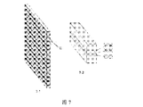
- FIG. 7 is a schematic structural diagram of a strip-shaped optical waveguide array plate in Embodiment 1 of the present invention, where 7-1 is a schematic structural diagram of a strip-shaped optical waveguide array plate, and 7-2 is a partially enlarged view of a region II.
- FIG. 8 is a schematic diagram of imaging of two sets of optical waveguide array plates IM1 and IM2 in Embodiment 2 of the present invention.
- Fig. 9 is a schematic diagram of light reflection and focusing imaging inside an optical waveguide, where A / B indicates the orientation on both sides.
- FIG. 10 is a schematic diagram of disassembly and imaging of the two sets of optical waveguide array plates of FIG. 8, where 10-1 is a schematic diagram of the unidirectional imaging light convergence of the IM1 optical waveguide array plate, and 10-2 is the unidirectional imaging light convergence of the IM2 optical waveguide array plate Schematic.
- Fig. 11 is a schematic diagram of the principle of stray light and imaging light generated by an optical waveguide, where A / B indicates the orientation on both sides, b indicates a stray light beam, and b 'indicates an imaging light beam.
- FIG. 12 is a schematic diagram of the principle that each unit of the optical waveguide array is equivalent to a cube R.
- B1, b3, and b4 are all stray light beams
- b2 is an imaging beam
- a is an object beam.
- FIG. 13 is a schematic diagram of the principle of avoiding the influence of stray light after the cube R of FIG. 12 is rotated by 45 °, where b1, b3, and b4 are all stray light beams, b2 is an imaging beam, and a is an object beam.
- This embodiment provides a processing technology of a single-row multi-row equivalent negative refractive index flat lens, including:
- the thickness of the cut sheet material is 3mm ⁇ d ⁇ 4mm.
- the thickness control can reduce unnecessary material waste on the one hand, and can be used for subsequent repairs.
- the mill provides a margin.
- the thickness of the parallel flat plate after polishing is d ⁇ 1.5mm.
- the thickness of the final processed parallel flat plate is related to the imaging quality. The smaller the thickness, the smaller the single pixel size of the focused imaging, and the higher the imaging clarity.
- strip-shaped optical waveguide array plate is coated with a protective layer and cut, it is cut into two sets of optical waveguide array plates as shown by IM1 and IM22 in FIG. 2.
- glue the two sets of optical waveguide array plates of 8) in such a way that the arrangement directions are perpendicular to each other.
- the type of glue may be transparent glue materials such as photosensitive glue and heat-sensitive glue.
- the invention relates to two core imaging elements IM1 and IM2, two orthogonal single-row multiple-row equivalent negative refractive index optical waveguide array plates, as shown in FIG. 8, which can realize square-to-point aberration-free imaging of object images.
- the specific principle is shown in Fig. 9.
- the object-side light on the A side is reflected by the equivalent negative refractive index flat lens optical waveguide. There is one or more reflections. It transmits the light beam to the B-side image side and modulates it into Mirror the light and refocus the image.
- IM1 and IM2 are disassembled. As shown in FIG.
- the imaging effect is consistent with a flat lens made of a negative refractive index material (refer to FIG. 8). Since the optical waveguide of this method can only partially modulate the object light, as shown in FIG. 11, the mirror-modulated light b 'participates in imaging, and the b light will maintain the original light characteristics and form stray light.
- Each unit that combines two mutually orthogonal two sets of optical waveguides is equivalent to a square waveguide for stray light analysis. As shown in Figure 12, the combined waveguide generates four beams of light on the image side, at least two of which reach the image plane. A beam participates in imaging and a beam affects imaging as stray light. In order to avoid the stray light shown in FIG.
- the two sets of optical waveguide arrays need to be rotated 45 ° and arranged orthogonally to each other, thereby eliminating the effect of stray light, as shown in FIG. 13.
- the final imaging effect of this imaging principle is consistent with a flat lens made of a negative refractive index material.
- the specific implementation of the present invention mainly describes the processing technology of single-row and multi-row equivalent negative refractive index flat lens and the imaging principle of the flat lens.
- the equivalent negative refractive index flat lens manufactured according to the processing process of the present invention each optical waveguide The difference between them is small, which greatly reduces the image clipping defects caused by the differences between the waveguides.
- the materials used for the flat lens of the present invention can be conventional optical materials, and high precision machining can be achieved in a short time by using this processing technology.
- the strip-shaped optical waveguide is coated on both sides, which avoids the effects of defects such as bubbles and impurities generated during the gluing process on imaging, and greatly reduces the difficulty of the gluing process. At the same time as high-definition imaging, mass production is easy and the cost is low.
Landscapes
- Physics & Mathematics (AREA)
- Engineering & Computer Science (AREA)
- General Physics & Mathematics (AREA)
- Optics & Photonics (AREA)
- Health & Medical Sciences (AREA)
- Manufacturing & Machinery (AREA)
- Ophthalmology & Optometry (AREA)
- Mechanical Engineering (AREA)
- Multimedia (AREA)
- Signal Processing (AREA)
- Optical Integrated Circuits (AREA)
Abstract
La présente invention concerne une technologie de traitement pour une lentille à lames à indice de réfraction négatif équivalente à une colonne unique et des rangées multiples, comprenant : la transformation d'un matériau optique en lames parallèles dont les surfaces supérieure et inférieure sont des surfaces polies ; la conduite d'une coupe le long d'un bord des lames parallèles pour obtenir des guides d'ondes optiques en forme de bande ; le placage d'un film d'aluminium recouvrant chacune des deux surfaces polies de chaque guide d'ondes optiques en forme de bande ; la liaison des surfaces plaquées des guides d'ondes optiques en forme de bande les unes aux autres pour former un réseau de guides d'ondes optiques en forme de bande à colonne unique et à rangées multiples ; le trempage du réseau de guides d'ondes optiques en forme de bande dans un adhésif thermosensible et le pressage de celui-ci pour évacuer les bulles d'air et l'excès de colle entre des surfaces liées ; le durcissement du réseau de guides d'ondes optiques en forme de bande au moyen d'un processus de chauffage ; la découpe des lames de réseau de guides d'ondes optiques en forme de bande en deux ensembles de lames de réseau de guides d'ondes optiques en forme de bande agencées dans une direction à 45 degrés ; et l'obtention d'une lentille à lames à indice de réfraction négatif équivalente à une colonne unique et des rangées multiples par collage des deux ensembles de lames de réseau de guides d'ondes optiques en forme de bande de sorte que leurs directions d'agencement soient perpendiculaires l'une par rapport à l'autre, puis l'ajout d'une feuille de fenêtre de protection sur chacun des deux côtés des deux ensembles de lames collés. La présente invention réduit considérablement les différences individuelles entre des guides d'ondes optiques en forme de bande traités selon une méthode de traitement conventionnelle, de façon à obtenir une imagerie tridimensionnelle claire d'un réseau épissé.
Priority Applications (2)
| Application Number | Priority Date | Filing Date | Title |
|---|---|---|---|
| EP18925489.9A EP3779522A4 (fr) | 2018-07-04 | 2018-07-17 | Technologie de traitement pour lentille à lames à indice de réfraction négatif équivalente à une colonne unique et des rangées multiples |
| US17/030,502 US11977242B2 (en) | 2018-07-04 | 2020-09-24 | Processing technology for single-column and multi-row equivalent negative refractive index plate lens |
Applications Claiming Priority (2)
| Application Number | Priority Date | Filing Date | Title |
|---|---|---|---|
| CN201810726637.7A CN110687621A (zh) | 2018-07-04 | 2018-07-04 | 一种单列多排等效负折射率平板透镜的加工工艺 |
| CN201810726637.7 | 2018-07-04 |
Related Child Applications (1)
| Application Number | Title | Priority Date | Filing Date |
|---|---|---|---|
| US17/030,502 Continuation US11977242B2 (en) | 2018-07-04 | 2020-09-24 | Processing technology for single-column and multi-row equivalent negative refractive index plate lens |
Publications (1)
| Publication Number | Publication Date |
|---|---|
| WO2020006780A1 true WO2020006780A1 (fr) | 2020-01-09 |
Family
ID=69060597
Family Applications (1)
| Application Number | Title | Priority Date | Filing Date |
|---|---|---|---|
| PCT/CN2018/095950 Ceased WO2020006780A1 (fr) | 2018-07-04 | 2018-07-17 | Technologie de traitement pour lentille à lames à indice de réfraction négatif équivalente à une colonne unique et des rangées multiples |
Country Status (4)
| Country | Link |
|---|---|
| US (1) | US11977242B2 (fr) |
| EP (1) | EP3779522A4 (fr) |
| CN (1) | CN110687621A (fr) |
| WO (1) | WO2020006780A1 (fr) |
Families Citing this family (7)
| Publication number | Priority date | Publication date | Assignee | Title |
|---|---|---|---|---|
| CN110716248B (zh) * | 2018-07-12 | 2021-03-09 | 安徽省东超科技有限公司 | 一种多列多排等效负折射率平板透镜的加工工艺 |
| CN114252941A (zh) * | 2020-09-21 | 2022-03-29 | 郭生文 | 一种光波导透镜 |
| CN113534303B (zh) * | 2021-06-22 | 2022-07-08 | 浙江蓝特光学股份有限公司 | 一种胶合棱镜的加工方法 |
| CN114637127A (zh) * | 2022-02-24 | 2022-06-17 | 安徽省东超科技有限公司 | 应用于光学成像系统的视场控制装置以及光学成像系统 |
| CN114815501B (zh) * | 2022-04-22 | 2025-09-12 | 安徽省东超科技有限公司 | 平板透镜的加工方法 |
| CN116203657A (zh) * | 2023-02-10 | 2023-06-02 | 安徽省东超科技有限公司 | 等效负折射率平板透镜及其制备方法 |
| CN118046605B (zh) * | 2024-02-27 | 2024-08-09 | 湖北五方晶体有限公司 | 一种光学棱镜集成双抛加工工艺 |
Citations (5)
| Publication number | Priority date | Publication date | Assignee | Title |
|---|---|---|---|---|
| CN1103630A (zh) * | 1993-12-10 | 1995-06-14 | 卢大伟 | 转移法制作彩虹玻璃的方法 |
| JP2001074989A (ja) * | 1999-07-23 | 2001-03-23 | Eastman Kodak Co | 合成像に対して周期構造を有するアレイを精確に配置する改良された方法及びその装置 |
| JP2004302121A (ja) * | 2003-03-31 | 2004-10-28 | Canon Inc | 立体画像表示装置、及び立体画像撮像装置 |
| CN1600724A (zh) * | 2004-09-29 | 2005-03-30 | 崔建伟 | 一种按太阳高度角选择采光功能玻璃 |
| CN107807417A (zh) * | 2017-12-09 | 2018-03-16 | 安徽省东超科技有限公司 | 单列多排等效负折射率平板透镜 |
Family Cites Families (8)
| Publication number | Priority date | Publication date | Assignee | Title |
|---|---|---|---|---|
| US5150259A (en) | 1990-07-30 | 1992-09-22 | Mitsubishi Rayon Company Ltd. | Optical imaging device |
| US10073264B2 (en) * | 2007-08-03 | 2018-09-11 | Lumus Ltd. | Substrate-guide optical device |
| JP5073609B2 (ja) | 2008-08-11 | 2012-11-14 | 日東電工株式会社 | 光導波路の製造方法 |
| CN102109638A (zh) | 2011-03-14 | 2011-06-29 | 浙江大学 | 一种玻璃热极化层中的条形光波导 |
| CN204029962U (zh) | 2014-08-14 | 2014-12-17 | 东南大学 | 基于超材料的折射率梯度平板聚焦透镜 |
| JP6165206B2 (ja) * | 2015-09-08 | 2017-07-19 | 松浪硝子工業株式会社 | 光制御パネルの製造方法、光制御パネル、光学結像装置、及び、空中映像形成システム |
| CN107831558A (zh) * | 2017-12-09 | 2018-03-23 | 安徽省东超科技有限公司 | 多排多列等效负折射率平板透镜 |
| CN108233863A (zh) | 2018-03-01 | 2018-06-29 | 成都银顶科技有限公司 | 条形聚光均光太阳能发电技术 |
-
2018
- 2018-07-04 CN CN201810726637.7A patent/CN110687621A/zh active Pending
- 2018-07-17 WO PCT/CN2018/095950 patent/WO2020006780A1/fr not_active Ceased
- 2018-07-17 EP EP18925489.9A patent/EP3779522A4/fr active Pending
-
2020
- 2020-09-24 US US17/030,502 patent/US11977242B2/en active Active
Patent Citations (5)
| Publication number | Priority date | Publication date | Assignee | Title |
|---|---|---|---|---|
| CN1103630A (zh) * | 1993-12-10 | 1995-06-14 | 卢大伟 | 转移法制作彩虹玻璃的方法 |
| JP2001074989A (ja) * | 1999-07-23 | 2001-03-23 | Eastman Kodak Co | 合成像に対して周期構造を有するアレイを精確に配置する改良された方法及びその装置 |
| JP2004302121A (ja) * | 2003-03-31 | 2004-10-28 | Canon Inc | 立体画像表示装置、及び立体画像撮像装置 |
| CN1600724A (zh) * | 2004-09-29 | 2005-03-30 | 崔建伟 | 一种按太阳高度角选择采光功能玻璃 |
| CN107807417A (zh) * | 2017-12-09 | 2018-03-16 | 安徽省东超科技有限公司 | 单列多排等效负折射率平板透镜 |
Non-Patent Citations (1)
| Title |
|---|
| See also references of EP3779522A4 * |
Also Published As
| Publication number | Publication date |
|---|---|
| EP3779522A4 (fr) | 2021-06-23 |
| CN110687621A (zh) | 2020-01-14 |
| US11977242B2 (en) | 2024-05-07 |
| US20210018658A1 (en) | 2021-01-21 |
| EP3779522A1 (fr) | 2021-02-17 |
Similar Documents
| Publication | Publication Date | Title |
|---|---|---|
| WO2020006780A1 (fr) | Technologie de traitement pour lentille à lames à indice de réfraction négatif équivalente à une colonne unique et des rangées multiples | |
| CN104035157B (zh) | 一种基于衍射光学元件的波导显示器 | |
| CN104350732B (zh) | 摄像装置 | |
| CN102047169B (zh) | 光学装置和结合光学装置的自动立体显示设备 | |
| US11092888B2 (en) | Processing method for multi-row, multi-column flat lens with equivalent negative refractive index | |
| WO2019109585A1 (fr) | Lentille en plaque à indice de réfraction négatif équivalente à de multiples rangées et de multiples colonnes | |
| WO2017219433A1 (fr) | Dispositif optique pour l'affichage d'un casque d'écoute à guide d'ondes | |
| JP2018513393A (ja) | 短距離光増幅モジュール、眼鏡、ヘルメット、および、vrシステム | |
| JP7659602B2 (ja) | 光導波路ユニット、アレイ及び平板レンズ | |
| CN104423050A (zh) | 裸眼立体显示装置 | |
| CN118330903B (zh) | 一种空中成像显示系统 | |
| CN110286494B (zh) | 光波导单元、阵列及平板透镜 | |
| CN207502759U (zh) | 多排多列等效负折射率平板透镜 | |
| CN107144973A (zh) | 紧凑型柱镜光栅式裸眼3d显示面板 | |
| CN113504604B (zh) | 一种扩瞳装置及ar设备 | |
| CN219302778U (zh) | 一种光机及可穿戴显示设备 | |
| CN117406404A (zh) | 一种折超红外偏振成像系统 | |
| CN210005808U (zh) | 光波导单元、阵列及平板透镜 | |
| CN110262047B (zh) | 光波导单元、阵列及平板透镜 | |
| US11977245B2 (en) | Optical waveguide unit, array, and flat lens | |
| TWM505616U (zh) | 3d顯示層及3d顯示結構 | |
| TW202518065A (zh) | 在自動立體顯示裝置中減少串擾 | |
| TWI579594B (zh) | 3d顯示層、3d顯示結構及其製作方法 |
Legal Events
| Date | Code | Title | Description |
|---|---|---|---|
| 121 | Ep: the epo has been informed by wipo that ep was designated in this application |
Ref document number: 18925489 Country of ref document: EP Kind code of ref document: A1 |
|
| ENP | Entry into the national phase |
Ref document number: 2018925489 Country of ref document: EP Effective date: 20201102 |
|
| NENP | Non-entry into the national phase |
Ref country code: DE |