WO2020008745A1 - 欠陥検出装置 - Google Patents
欠陥検出装置 Download PDFInfo
- Publication number
- WO2020008745A1 WO2020008745A1 PCT/JP2019/020086 JP2019020086W WO2020008745A1 WO 2020008745 A1 WO2020008745 A1 WO 2020008745A1 JP 2019020086 W JP2019020086 W JP 2019020086W WO 2020008745 A1 WO2020008745 A1 WO 2020008745A1
- Authority
- WO
- WIPO (PCT)
- Prior art keywords
- contact
- wave
- vibration
- elastic wave
- inspected
- Prior art date
- Legal status (The legal status is an assumption and is not a legal conclusion. Google has not performed a legal analysis and makes no representation as to the accuracy of the status listed.)
- Ceased
Links
Images






Classifications
-
- G—PHYSICS
- G01—MEASURING; TESTING
- G01N—INVESTIGATING OR ANALYSING MATERIALS BY DETERMINING THEIR CHEMICAL OR PHYSICAL PROPERTIES
- G01N29/00—Investigating or analysing materials by the use of ultrasonic, sonic or infrasonic waves; Visualisation of the interior of objects by transmitting ultrasonic or sonic waves through the object
- G01N29/04—Analysing solids
- G01N29/045—Analysing solids by imparting shocks to the workpiece and detecting the vibrations or the acoustic waves caused by the shocks
-
- G—PHYSICS
- G01—MEASURING; TESTING
- G01N—INVESTIGATING OR ANALYSING MATERIALS BY DETERMINING THEIR CHEMICAL OR PHYSICAL PROPERTIES
- G01N29/00—Investigating or analysing materials by the use of ultrasonic, sonic or infrasonic waves; Visualisation of the interior of objects by transmitting ultrasonic or sonic waves through the object
- G01N29/04—Analysing solids
- G01N29/041—Analysing solids on the surface of the material, e.g. using Lamb, Rayleigh or shear waves
-
- G—PHYSICS
- G01—MEASURING; TESTING
- G01B—MEASURING LENGTH, THICKNESS OR SIMILAR LINEAR DIMENSIONS; MEASURING ANGLES; MEASURING AREAS; MEASURING IRREGULARITIES OF SURFACES OR CONTOURS
- G01B11/00—Measuring arrangements characterised by the use of optical techniques
- G01B11/16—Measuring arrangements characterised by the use of optical techniques for measuring the deformation in a solid, e.g. optical strain gauge
- G01B11/161—Measuring arrangements characterised by the use of optical techniques for measuring the deformation in a solid, e.g. optical strain gauge by interferometric means
- G01B11/162—Measuring arrangements characterised by the use of optical techniques for measuring the deformation in a solid, e.g. optical strain gauge by interferometric means by speckle- or shearing interferometry
-
- G—PHYSICS
- G01—MEASURING; TESTING
- G01B—MEASURING LENGTH, THICKNESS OR SIMILAR LINEAR DIMENSIONS; MEASURING ANGLES; MEASURING AREAS; MEASURING IRREGULARITIES OF SURFACES OR CONTOURS
- G01B9/00—Measuring instruments characterised by the use of optical techniques
- G01B9/02—Interferometers
- G01B9/02094—Speckle interferometers, i.e. for detecting changes in speckle pattern
- G01B9/02095—Speckle interferometers, i.e. for detecting changes in speckle pattern detecting deformation from original shape
-
- G—PHYSICS
- G01—MEASURING; TESTING
- G01B—MEASURING LENGTH, THICKNESS OR SIMILAR LINEAR DIMENSIONS; MEASURING ANGLES; MEASURING AREAS; MEASURING IRREGULARITIES OF SURFACES OR CONTOURS
- G01B9/00—Measuring instruments characterised by the use of optical techniques
- G01B9/02—Interferometers
- G01B9/02097—Self-interferometers
-
- G—PHYSICS
- G01—MEASURING; TESTING
- G01N—INVESTIGATING OR ANALYSING MATERIALS BY DETERMINING THEIR CHEMICAL OR PHYSICAL PROPERTIES
- G01N21/00—Investigating or analysing materials by the use of optical means, i.e. using sub-millimetre waves, infrared, visible or ultraviolet light
- G01N21/84—Systems specially adapted for particular applications
- G01N21/88—Investigating the presence of flaws or contamination
- G01N21/8806—Specially adapted optical and illumination features
-
- G—PHYSICS
- G01—MEASURING; TESTING
- G01N—INVESTIGATING OR ANALYSING MATERIALS BY DETERMINING THEIR CHEMICAL OR PHYSICAL PROPERTIES
- G01N29/00—Investigating or analysing materials by the use of ultrasonic, sonic or infrasonic waves; Visualisation of the interior of objects by transmitting ultrasonic or sonic waves through the object
- G01N29/22—Details, e.g. general constructional or apparatus details
- G01N29/24—Probes
- G01N29/2418—Probes using optoacoustic interaction with the material, e.g. laser radiation, photoacoustics
-
- G—PHYSICS
- G01—MEASURING; TESTING
- G01N—INVESTIGATING OR ANALYSING MATERIALS BY DETERMINING THEIR CHEMICAL OR PHYSICAL PROPERTIES
- G01N29/00—Investigating or analysing materials by the use of ultrasonic, sonic or infrasonic waves; Visualisation of the interior of objects by transmitting ultrasonic or sonic waves through the object
- G01N29/22—Details, e.g. general constructional or apparatus details
- G01N29/24—Probes
- G01N29/2437—Piezoelectric probes
-
- G—PHYSICS
- G01—MEASURING; TESTING
- G01N—INVESTIGATING OR ANALYSING MATERIALS BY DETERMINING THEIR CHEMICAL OR PHYSICAL PROPERTIES
- G01N29/00—Investigating or analysing materials by the use of ultrasonic, sonic or infrasonic waves; Visualisation of the interior of objects by transmitting ultrasonic or sonic waves through the object
- G01N29/44—Processing the detected response signal, e.g. electronic circuits specially adapted therefor
- G01N29/4445—Classification of defects
-
- G—PHYSICS
- G01—MEASURING; TESTING
- G01J—MEASUREMENT OF INTENSITY, VELOCITY, SPECTRAL CONTENT, POLARISATION, PHASE OR PULSE CHARACTERISTICS OF INFRARED, VISIBLE OR ULTRAVIOLET LIGHT; COLORIMETRY; RADIATION PYROMETRY
- G01J9/00—Measuring optical phase difference; Determining degree of coherence; Measuring optical wavelength
- G01J9/02—Measuring optical phase difference; Determining degree of coherence; Measuring optical wavelength by interferometric methods
- G01J9/0215—Measuring optical phase difference; Determining degree of coherence; Measuring optical wavelength by interferometric methods by shearing interferometric methods
-
- G—PHYSICS
- G01—MEASURING; TESTING
- G01N—INVESTIGATING OR ANALYSING MATERIALS BY DETERMINING THEIR CHEMICAL OR PHYSICAL PROPERTIES
- G01N21/00—Investigating or analysing materials by the use of optical means, i.e. using sub-millimetre waves, infrared, visible or ultraviolet light
- G01N21/84—Systems specially adapted for particular applications
- G01N21/88—Investigating the presence of flaws or contamination
- G01N21/8806—Specially adapted optical and illumination features
- G01N2021/8838—Stroboscopic illumination; synchronised illumination
-
- G—PHYSICS
- G01—MEASURING; TESTING
- G01N—INVESTIGATING OR ANALYSING MATERIALS BY DETERMINING THEIR CHEMICAL OR PHYSICAL PROPERTIES
- G01N2291/00—Indexing codes associated with group G01N29/00
- G01N2291/01—Indexing codes associated with the measuring variable
- G01N2291/012—Phase angle
-
- G—PHYSICS
- G01—MEASURING; TESTING
- G01N—INVESTIGATING OR ANALYSING MATERIALS BY DETERMINING THEIR CHEMICAL OR PHYSICAL PROPERTIES
- G01N2291/00—Indexing codes associated with group G01N29/00
- G01N2291/04—Wave modes and trajectories
- G01N2291/042—Wave modes
- G01N2291/0422—Shear waves, transverse waves, horizontally polarised waves
-
- G—PHYSICS
- G01—MEASURING; TESTING
- G01N—INVESTIGATING OR ANALYSING MATERIALS BY DETERMINING THEIR CHEMICAL OR PHYSICAL PROPERTIES
- G01N2291/00—Indexing codes associated with group G01N29/00
- G01N2291/04—Wave modes and trajectories
- G01N2291/042—Wave modes
- G01N2291/0427—Flexural waves, plate waves, e.g. Lamb waves, tuning fork, cantilever
Definitions
- the present invention relates to a defect detection device for detecting a defect of an object such as a concrete or a steel structure.
- Laser ultrasonic method is one of the techniques for detecting the surface and internal defects of objects such as concrete and steel structures.
- the surface displacement is measured by exciting the vibration of an elastic wave in the object to be inspected, irradiating the object to be inspected with laser light in that state, and detecting the reflected light with a laser interferometer. Since the surface displacement due to vibration changes discontinuously at the defect, the defect can be detected by measuring the distribution of the surface displacement.
- the detection laser (probe laser) of the laser interferometer is point-shaped, it is necessary to scan over the entire inspection area of the object to be inspected, which takes a long time.
- Speckle interferometry splits laser light from a laser light source into illumination light and reference light, performs strobe illumination on the inspection area using the illumination light, and the illumination light is applied to each point on the surface of the inspected object in the inspection area.
- Speckle-sharing interferometry uses a laser beam from a laser light source (does not split the reference beam) to illuminate the inspection area with strobe light, and reflects light from two adjacent points on the surface of the inspection object in the inspection area. This is to obtain an interference pattern due to incoming light.
- an elastic wave is input to the object to be inspected, images of the interference pattern are respectively taken before and after input by a CCD camera or the like, and the two images are used to determine the front-back direction (surface) of the inspection area.
- the distribution of the displacement (outward) or the relative displacement is calculated. Since the displacement or the relative displacement becomes discontinuous at the position of the defect, the defect existing in the inspection area can be detected.
- these methods only look at one state of the elastic wave, if the wavelength of the elastic wave is smaller than the inspection area, it is easy to detect if the defect happens to be in the part where the amplitude of the wave is large. However, if it exists in a portion where the amplitude is small, it is difficult to detect. That is, a difference occurs in the defect inspection capability depending on the location in the inspection area.
- Patent Document 1 discloses that in a defect detection method using speckle interferometry or speckle shearing interferometry, while exciting a continuous wave of an elastic wave to an inspected object, It describes that the displacement of each point (speckle interferometry) or the relative displacement between two adjacent points (speckle sharing interferometry) is measured in three phases. This makes it possible to reproduce the entire vibration state of the elastic wave at any location in the inspection area, regardless of the relationship between the size of the inspection area and the wavelength of the elastic wave, without depending on the location in the inspection area. Defects can be accurately detected.
- the problem to be solved by the present invention is to provide a defect detection device capable of detecting not only a defect outside an observable range but also a defect outside an observable range from among the inspected objects. That is.
- a defect detection device made to solve the above problem, An excitation source that can be arranged at an arbitrary position on the surface of the object to be inspected and within the object to be inspected, which excites an elastic wave in which one vibration mode is dominant and travels in a predetermined direction.
- an illumination unit that performs strobe illumination on an illumination area on the surface of the inspection object, Speckle interferometry or speckle-sharing interferometry, a displacement measuring unit that collectively measures the longitudinal displacement of each point in the illumination region in at least three different phases of the elastic wave, And a reflected wave / scattered wave detector for detecting one or both of a reflected wave and a scattered wave of the elastic wave based on the displacement measured by the displacement measuring unit.
- the excitation source is arranged at an arbitrary position on the inspection object, and a certain vibration mode is dominant and directed in a predetermined direction from the excitation source into the inspection object.
- a certain vibration mode is dominant and directed in a predetermined direction from the excitation source into the inspection object.
- the position of the excitation source and / or the movement of the elastic wave in the traveling direction are performed so that one vibration mode is dominant and travels in a predetermined direction.
- Strobe illumination is performed on the illumination area by the illumination unit while exciting the elastic wave, and the displacement measurement unit uses speckle interferometry or speckle sharing interferometry to front and rear directions of each point in the illumination area (illumination unit). , Or away from the illumination unit).
- the displacement measurement unit measures the displacement of each point in the front-rear direction in at least three different phases to reproduce the entire vibration state of the elastic wave at each point in the illumination area.
- the illumination area may be the entire surface of the inspection object or a part thereof.
- the illumination area is, of course, a part (all or a part) of the part observing the shielding area. In this way, the displacement in the front-back direction of each point in the illumination area is collectively measured, and the amplitude and phase of the vibration of each point are obtained from the displacement.
- the reflected wave / scattered wave detection unit an image is created based on the amplitude and phase values of the vibration at each point, and an image processing technique is used for the created image, or the inspector looks at the image. Detect reflected and / or scattered waves.
- the position of the defect can be specified from the position of the excitation source and the traveling direction of the elastic wave, and the traveling direction of the reflected wave and / or the scattered wave.
- an elastic wave from the excitation source and a reflected wave of the elastic wave reflected at an end of the object to be inspected are also observed. And reflected waves and / or scattered waves generated by defects.
- the defect detection device even when a defect exists outside the illumination area, a reflected wave or a scattered wave that is reflected or scattered by the defect and travels through the illumination area is measured in the illumination area. Thereby, the defect can be detected. This makes it possible to detect a defect outside the observable range, such as a portion covered by the shielding member.
- the displacement in the front-rear direction is measured by using the speckle interferometry or the speckle sharing interferometry as described above, and the speckle sharing interferometry measures the displacement at a certain point. Since the two lights for measurement pass through substantially the same optical path, they have a feature that they are less susceptible to environmental disturbance due to the difference in the passing environment than the speckle interferometry in which the measuring light and the reference light pass through different places. Although the minimum number of phases required for obtaining the reflected and / or scattered wave waveforms is three, increasing the number of phases to be measured to more than three increases the accuracy of the obtained waveforms. It can be even higher.
- the excitation source of the first example has a case in which a plurality of contact portions to be brought into contact with the surface of the object to be inspected are arranged at equal intervals, and an elastic wave having a wavelength of the same length as the interval is generated in the object to be inspected. And a vibration applying section for applying vibration having the same frequency as that of the elastic wave in the contact section. After such a contact is brought into contact with the surface of the object to be inspected, vibration is applied from the vibration applying section to the contact so that the contact points in a direction in which the contact portions are arranged and proceeds along the surface of the object to be inspected. Elastic waves can be generated.
- the object to be inspected can be strongly excited and the amplitude of the elastic wave can be increased.
- the amplitude of the elastic wave By increasing the amplitude of the elastic wave in this manner, a defect can be detected with high sensitivity.
- a space may be provided between a plurality of contact portions arranged at equal intervals, but a second contact portion may be provided between two adjacent contact portions of the plurality of contact portions.
- the vibration applying section applies vibrations at phases different from each other by 180 ° between the contact section and the second contact section.
- vibration can be applied to the surface of the object to be inspected from both the contact portion and the second contact portion in accordance with the spatial phase of the elastic wave generated on the surface of the object to be inspected. Can be increased.
- the excitation source of the second example is used when the object to be inspected has a plate shape, and includes a contact portion having a contact surface that contacts the surface of the object to be inspected, A vibration imparting unit that imparts vibration to the contact unit, which propagates in the inclined direction and excites an elastic wave having a wavelength coincident with a wavelength of a vibration mode that can be generated in the inspection object into the contact unit.
- a vibration imparting unit that imparts vibration to the contact unit, which propagates in the inclined direction and excites an elastic wave having a wavelength coincident with a wavelength of a vibration mode that can be generated in the inspection object into the contact unit.
- the contact portion is made of a material having a smaller acoustic impedance difference from the object to be inspected than the vibration applying portion.
- the second contact portion is made of a material having a smaller acoustic impedance difference from the object to be inspected than the vibration applying portion.
- the contact portion is made of a material having a smaller acoustic impedance difference from the object to be inspected than the vibration applying portion.
- a Lamb wave has both vibration components in a direction perpendicular to the propagation direction and a direction parallel to the propagation direction, is a wave in which longitudinal waves and transverse waves are mixed, and has a velocity dispersibility such that a phase velocity changes according to a frequency, and , And has a feature that it can take a plurality of vibration modes having different relationships between frequency and phase velocity.
- a vibration mode having a high frequency can be selected without reducing the efficiency of exciting the object to be inspected, and the wavelength of the elastic wave in the object to be inspected can be selected. Can be shortened. As described above, by reducing the wavelength of the elastic wave in the object to be inspected, the elastic wave can be reflected or scattered even for a small defect, and the defect can be detected more reliably.
- the defect detection device can detect not only a defect that is outside the observable range but also a defect that is outside the observable range among the inspected objects.
- FIG. 1 is a schematic configuration diagram showing a first embodiment of a defect detection device according to the present invention.
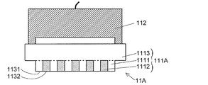
- FIG. 3 is a longitudinal sectional view showing an example of an excitation source used in the defect detection device according to the first embodiment.
- FIG. 4 is a longitudinal sectional view showing a modification of the excitation source used in the defect detection device according to the first embodiment.
- 5 is a flowchart illustrating the operation of the defect detection device according to the first embodiment.
- FIG. 4 is a schematic diagram illustrating an operation of an example of an excitation source used in the defect detection device according to the first embodiment.
- FIG. 6 is a schematic diagram showing an operation of a modification of the excitation source used in the defect detection device according to the first embodiment.
- FIG. 4 is a graph for explaining the principle of a defect inspection performed by the defect detection device according to the first embodiment.
- FIG. 4 is a schematic diagram illustrating an example of an elastic wave observed in an illumination area.
- FIG. 2 is a schematic configuration diagram showing a second embodiment of the defect detection device according to the present invention.
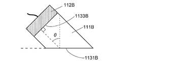
- FIG. 9 is a vertical cross-sectional view illustrating an example of an excitation source used in the defect detection device according to the second embodiment.
- FIG. 9 is a schematic diagram showing the operation of an excitation source used in the defect detection device according to the second embodiment.
- 9 is a dispersion curve showing a relationship between a frequency and a phase velocity of a Lamb wave generated in a steel plate having a thickness of 10 mm.
- 9 is a graph showing the relationship between the frequency of vibration and the angle of incidence when a copper contact according to the second embodiment is used.
- FIG. 1 is a schematic configuration diagram of a defect detection device 10 of the first embodiment.
- the defect detection apparatus 10 includes an excitation source 11, a signal generator 12, a pulse laser light source 13, an illumination light lens 14, a speckle / sharing interferometer 15, a reflected / scattered wave detector 16, a controller 17, and a memory.
- a section 18 is provided.
- the excitation source 11 has a contact 111 and a vibration imparting unit 112 as shown in FIG. 2A.
- the contact 111 has a contact portion 1111 and a base 1113. It is desirable that the contact portion 1111 be made of the same material as the object to be inspected or a material having an acoustic impedance closer to that of the material of the object to be inspected than the vibration imparting portion 112.
- a steel plate is used as the inspection object S
- iron is used as the material of the contact portion 1111
- ceramics are used for the vibration applying portion 112.
- the value of the acoustic impedance of the iron used for the contact 111 is closer to the value of the steel of the object S to be inspected than the value of the ceramic of the vibration applying unit 112.
- the contact portion 1111 has a rod-like shape having a rectangular or square cross section, and a plurality of the contact portions 1111 are arranged at equal intervals in a direction (horizontal direction in FIG. 2A) perpendicular to the longitudinal direction (direction perpendicular to the paper surface in FIG. 2A). Lined up.
- the base 1113 is a single rectangular parallelepiped member made of the same material as the contact portion 1111.
- One of the four surfaces (including one side of a rectangular or square cross section) of the contact portion 1111 is a contact surface 1131 that makes contact with the surface of the inspection object S, and the surface facing the contact surface 1131 is a base. 1113 is in contact with one surface.
- the contact portion 1111 and the base portion 1113 are formed as one body.
- the space between the adjacent contact portions 1111 is a space (air) in the contact 111 of this example.
- the distance between adjacent contact portions 1111 is 8 mm in the present embodiment. This interval was set to match the wavelength of an elastic wave having a frequency of 360 kHz (described later) generated in a steel plate as an object to be inspected.
- a second contact portion 1112 is provided like a contact 111A in an excitation source 11A of a modification shown in FIG. 2B. It may be.
- Second contact portion 1112 is made of tin, which is a different material from contact portion 1111. Since the speed at which the sound wave (vibration) propagates is different between iron (longitudinal wave speed 5950 m / s), which is the material of the contact portion 1111, and tin (3230 m / s), which is the material of the second contact portion 1112.
- the vibration applying unit 112 is made of a piezoelectric element, and is in contact with a surface of the base 1113 of the contact 111 that faces the surface that contacts the contact unit 1111.
- the vibration applying section 112 is connected to the signal generator 12 by a cable.
- the signal generator 12 generates an AC electric signal of a predetermined frequency and transmits the signal to the vibration applying unit 112 of the excitation source 11. In the present embodiment, this frequency is 360 kHz as described above. With this AC electric signal, the vibration applying unit 112 vibrates at the predetermined frequency to apply vibration to the contact unit 1111, and the contact surface 1131 (or the contact surfaces 1131 and 1132 when the contact 111 ⁇ / b> A is used) through the contact unit 1111. And the vibration is propagated to the surface of the inspection object S.
- the signal generator 12 is also connected to the pulse laser light source 13 by a cable different from the cable connected to the vibration applying unit 112, and the signal generator 12 supplies the pulse laser light source 13 at a timing when the AC electric signal has a predetermined phase.
- a pulse-like electric signal (pulse signal) is transmitted.
- the predetermined phase and the timing determined thereby are changed during the defect inspection as described later.
- the pulse laser light source 13 is a light source that outputs a pulse laser light when receiving a pulse signal from the signal generator 12.
- the illumination light lens 14 is disposed between the pulse laser light source 13 and the surface of the inspection object S, and includes a concave lens.
- the illumination light lens 14 has a role of spreading the pulse laser light from the pulse laser light source 13 over the entire illumination area L on the surface of the inspection object S.
- the illumination area L is an area excluding a portion of the surface of the inspection object S that is hidden by the obstacle (shielding member) B from the illumination light lens 14.
- the obstacle B includes, for example, the above-described reinforcing member.
- the pulse laser light source 13 and the illumination light lens 14 correspond to the illumination unit described above.
- the speckle-sharing interferometer 15 corresponds to the above-described displacement measuring unit, and includes a beam splitter 151, a first reflecting mirror 1521, a second reflecting mirror 1522, a phase shifter 153, a condenser lens 154, and an image sensor 155.
- the beam splitter 151 is a half mirror arranged at a position where the illumination light reflected on the illumination area L on the surface of the inspection object S enters.
- the first reflecting mirror 1521 is arranged on the optical path of the illumination light reflected by the beam splitter 151, and the second reflecting mirror 1522 is arranged on the optical path of the illumination light transmitted through the beam splitter 151.
- the phase shifter 153 is disposed between the beam splitter 151 and the first reflecting mirror 1521, and changes (shifts) the phase of light passing through the phase shifter 153.
- the image sensor 155 includes illumination light that is reflected by the first reflecting mirror 1521 and then passes through the beam splitter 151 after being reflected by the beam splitter 151, and is reflected by the second reflecting mirror 1522 after passing through the beam splitter 151 and is then reflected by the beam splitter. It is arranged on the optical path of the illumination light reflected at 151.
- the condenser lens 154 is disposed between the beam splitter 151 and the image sensor 155.
- the first reflecting mirror 1521 is arranged so that its reflecting surface is at an angle of 45 ° with respect to the reflecting surface of the beam splitter 151.
- the second reflecting mirror 1522 is arranged such that its reflecting surface is at an angle slightly inclined from 45 ° with respect to the reflecting surface of the beam splitter 151. Due to the arrangement of the first reflecting mirror 1521 and the second reflecting mirror 1522, the image sensor 155 causes the point P1 on the surface of the inspected object S and the illumination light reflected by the first reflecting mirror 1521 (one point in FIG. 1).
- the image sensor 155 has a large number of detection elements, and emits light incident on the image sensor 155 from a number of points (the points P1) on the surface of the inspection object S through the first reflecting mirror 1521 and the phase shifter 153. Detection is performed using different detection elements. Similarly, at the point P2, light incident on the image sensor 155 from the many points through the second reflecting mirror 1522 is detected by different detection elements.
- the reflected wave / scattered wave detection unit 16 obtains the vibration state (amplitude and phase) of the elastic wave at each point of the illumination area L based on the light detected by the image sensor 155, as described later, and based on the vibration state. A reflected wave and / or a scattered wave at the defect D is detected.
- the control unit 17 controls the signal generator 12 and performs data processing based on detection signals obtained from each detection element of the image sensor 155.
- the storage unit 18 stores a detection signal obtained from each detection element of the image sensor 155 and data processed by the control unit 17.
- FIG. 3 is a flowchart showing the operation of the defect detection apparatus 10
- FIGS. 4A and 4B are schematic diagrams showing the operation of the excitation sources 11 and 11A
- FIG. 5 is a graph for explaining the principle of the defect inspection performed by the defect detection apparatus 10.
- FIG. 6 is a schematic diagram showing an example of an elastic wave observed in the illumination area L.
- the measurement of the surface displacement is performed at m max ⁇ 3 times where the phases of the vibrations of the excitation source 11 are different.
- the “phase of vibration of the excitation source 11” is a phase of an AC electric signal transmitted from the signal generator 12 to the excitation source 11, and corresponds to a phase of an elastic wave at a certain point on the surface of the inspection object S. Equivalent to.
- the phase is shifted by a predetermined amount from the phase of the one point regardless of time.
- an initial value of k is set to 1 (step S1), and an AC electric signal is transmitted from the signal generator 12 to the excitation source 11, whereby vibration from the contact 111 of the excitation source 11 to the inspection object S is measured.
- the application is started (step S2).
- the vibration is applied to the inspection object S by first vibrating the piezoelectric element constituting the vibration applying unit 112 of the excitation source 11 by receiving the AC electric signal, and the vibration of the vibration applying unit 112 is controlled by a plurality of contact portions. This is performed by transmitting to the inspected object S in the same phase via each of the lines 1111.
- the excitation source 11 since the plurality of contact portions 1111 are arranged at equal intervals according to the wavelength of the elastic wave generated in the inspection object S as described above, the inspection object S has the wavelength.
- Elastic waves directed in the direction in which the plurality of contact portions 1111 are arranged are generated (FIG. 4A). In FIG. 4A, the wave of the vibration of the contact portion 1111 and the elastic wave generated in the inspection object S are drawn as transverse waves, but actually, these waves are longitudinal waves.
- the phase of the vibration transmitted to the surface of the inspected object S through the interface differs by 180 °.
- the pulse laser light source 13 Each time the pulse laser light source 13 receives a pulse signal, the pulse laser light source 13 repeatedly outputs illumination light that is a pulse laser light. This illumination light is expanded in diameter by the illumination light lens 14 and is applied to the entire illumination area L on the surface of the inspection object S (step S3).
- the illumination light is reflected on the surface of the inspection object S in the illumination area L and enters the beam splitter 151 of the speckle sharing interferometer 15.
- a part of the illuminating light is reflected by the beam splitter 151, passes through the phase shifter 153, is reflected by the first reflecting mirror 1521, passes through the phase shifter 153 again, and then passes through the beam splitter 151.
- the rest of the illumination light that has entered the beam splitter 151 passes through the beam splitter 151, is reflected by the second reflecting mirror 1522, and is partially reflected by the beam splitter 151 and enters the image sensor 155.
- illumination light reflected at a number of points on the surface of the inspection object S is detected by different detection elements.
- the phase shifter 153 changes (shifts) the phase of the illumination light passing through the phase shifter 153 (that is, the illumination light reflected at the point P1) while the illumination light as the pulse laser light is repeatedly output. Go on. As a result, the phase difference between the illumination light reflected at the point P1 and the illumination light reflected at the point P2 changes. During this change, each detection element of the image sensor 155 causes the two illumination lights to interfere with each other. The intensity of the generated interference light is detected (step S4). In the upper part of FIG. 5, the amount of phase shift by the phase shifter 153 obtained when the phase of the vibration of the excitation source 11 is ⁇ 0 and the intensity of the interference light detected by the detection element of the image sensor 155 are shown.
- FIG. 5 An example is shown in a graph.
- the relationship in which the detected intensity changes in a sinusoidal manner with respect to the phase shift amount is shown by a continuous curve, but what is actually observed is discrete data.
- the above continuous sine waveform is reproduced from the data by the least square method or the like. For that purpose, it is necessary to detect the intensity at at least three different phase shift amounts.
- step S5 it is confirmed whether or not the value of k has reached m max .
- the determination in step S5 is “NO”. If “NO”, the process proceeds to step S6, and the value of k is increased by 1 to “2” (the case where the determination in step S5 is “YES” will be described later).
- the signal generator 12 transmits a pulse signal to the pulse laser light source 13, and the pulse laser light source 13 repeatedly irradiates the surface of the inspection object S with illumination light, which is pulse laser light, at the timing of receiving the pulse signal. .
- the phase shifter 153 while changing (shifting) the phase of the illumination light reflected at the point P1 by the phase shifter 153 to at least three values, each detection element of the image sensor 155 is reflected at the point P1 and passed through the phase shifter 153 and the like.
- the intensity of the interference light between the illumination light and the illumination light reflected at the point P2 is detected (step S4).
- phase shifter 153 is a graph showing the amount of phase shift by the phase shifter 153 and the intensity of the interference light detected by the detection element of the image sensor 155, which are obtained when the phase of the vibration of the excitation source 11 is ⁇ 1.
- the peak position of the intensity of the interference light is shifted by ⁇ 1 ⁇ 0 in both cases.
- This shift indicates that the phase difference between the light from the point P1 and the light from the point P2 has changed due to the difference in the phase of the vibration of the excitation source 11 at the time of detection.
- This change in the phase difference of the optical path indicates that the relative displacement of the points P1 and P2 in the out-of-plane direction has changed.
- the relationship of the intensity of the shift amount and the interference light of the phase is obtained by the phase shifter 153 at the time the phase of the AC electrical signal is phi 2.
- step S5 since the value of k is 3 and has reached mmax , it is determined to be "YES”, and the process proceeds to step S7.
- step S7 the transmission of the AC electric signal from the signal generator 12 to the excitation source 11 is stopped, and thereby the vibration of the excitation source 11 is stopped.
- the reflected wave / scattered wave detection unit 16 obtains the vibration state (amplitude and phase) of the elastic wave at each point of the illumination area L by the following operation.
- the reflected wave / scattered wave detection unit 16 detects each detection element of the image sensor while changing the amount of phase shift by the phase shifter 153 in each of the phases ⁇ 0 , ⁇ 1 , and ⁇ 2 of the vibration.
- the maximum output phase shift amounts ⁇ 0 , ⁇ 1 , and ⁇ 2 at which the output of the element becomes maximum are obtained (see each graph in FIG. 5).
- the reflected wave / scattered wave detection unit 16 obtains the difference ( ⁇ 1 ⁇ 0 ), ( ⁇ 2 ⁇ 1 ), and ( ⁇ 0 - ⁇ 2 ) of the maximum output phase shift amounts having different phases of vibration. (Step S8).
- the difference between these three maximum output phase shift amounts indicates three sets of relative displacements of the points P1 and P2 in the out-of-plane direction with two sets of data having different phases (that is, different times) of the vibration of the excitation source 11. ing.
- the reflected wave / scattered wave detection unit 16 calculates three values of the vibration amplitude, vibration phase, and vibration center value (DC component) at each point in the illumination area L. The value of the parameter is obtained (step S9).
- the reflected wave / scattered wave detection unit 16 obtains the value of the displacement in the front-rear direction of each point at a certain time from the amplitude, phase, and center value of the vibration of each point thus obtained, and based on the value of the displacement, An image representing an elastic wave formed in the illumination area L is created (Step S10).
- an elastic wave can be represented by changing the luminance of a pixel corresponding to a point according to the displacement value of each point.
- step S11 the reflected wave / scattered wave detection unit 16 analyzes the image 20 thus created to detect a defect D as described below.
- an elastic wave shown in FIG. 6 appears.
- an elastic wave (oscillation wave 21) oscillated from the excitation source 11 appears in the image 20 as a wave directed in a direction in which the plurality of contact portions 1111 of the excitation source 11 are arranged.
- a reflected wave (end reflected wave 22) obtained by reflecting the oscillation wave 21 at the end of the inspection object S also appears in the image 20.
- the oscillation wave 21 and the end reflection wave 22 appear regardless of the presence or absence of the defect D in the inspection object S.
- the oscillation wave 21 is generated so as to be directed in a non-perpendicular direction with respect to the end surface of the inspection object S so that the oscillation wave 21 and the end reflected wave 22 do not overlap. .
- the image 20 further includes a reflected wave and / or a scattered wave reflected by the defect D (defect reflected / scattered wave 23). Appear in the image 20.
- the defect D when the defect D is outside the illumination area L because it is hidden by the obstacle B, the defect D cannot be directly observed.
- the defect reflected / scattered wave 23 reflected or scattered by the defect D can be used. Reaches the illumination region L, it can be specified that the defect D exists on the extension of the oscillation wave 21 and the defect reflected / scattered wave 23.
- the defect D does not exist before the oscillation wave 21 is directed from the excitation source 11.
- whether or not the defect D exists at any other position cannot be specified by only one operation up to this point.
- a defect may be detected by changing the position and / or direction of the excitation source 11 (the direction in which the oscillation wave 21 oscillates). Therefore, in step S12, it is determined whether the position and / or orientation of the excitation source 11 is changed.
- step S12 This determination may be made each time the operator operates an input device such as a keyboard, a mouse, a touch panel, or the like, or the number of times the position and / or direction of the excitation source 11 is changed or the magnitude of the change (excitation source 11 may be incorporated in the program and executed according to the program. If YES (change) is selected in step S12, the position and / or orientation of the excitation source 11 is automatically or manually changed in step S13, and the process returns to step S1 to perform the operations up to step S11. On the other hand, if NO (no change) is selected in step S12, a series of operations ends.
- NO no change
- an elastic wave having directivity is excited on the surface of the inspection object S using the excitation source 11, and the elastic wave is generated using the speckle-sharing interferometer 15.
- the defect reflected / scattered waves 23 reflected and / or scattered by the defect D not only the illumination area L but also the illumination area L such as a location covered with an obstacle (shielding member) B can be observed.
- An external defect D can also be detected.
- the excitation source 11 can generate an elastic wave having a wavelength corresponding to the interval between the contact portions 1111 with a large amplitude, the defect can be detected with high sensitivity. Can be. Further, by shortening the interval between the contact portions 1111, it is possible to prevent the amplitude of the elastic wave from being reduced even if the wavelength of the elastic wave is shortened, and it is possible to more reliably detect a small defect.
- the acoustic impedance of the material of the contact portion 1111 and the second contact portion 1112 is closer to the acoustic impedance of the material of the inspected object S than the acoustic impedance of the material of the vibration imparting portion 112, Efficient transmission of vibration contributes to increasing the amplitude of elastic waves.
- FIG. 7A is a schematic configuration diagram of a defect detection device 10B of the second embodiment.
- the defect detection device 10B has the same configuration as the defect detection device 10 of the first embodiment except that the excitation source 11B has a configuration different from the excitation sources 11 and 11A.
- the excitation source 11B has a contact (contact part) 111B and a vibration applying part 112B.
- the contact 111B has a contact surface 1131B that contacts the surface of the inspection object S and a receiving surface 1133B that contacts the vibration applying unit 112B and receives the vibration of the vibration applying unit 112B.
- the contact surface 1131B and the receiving surface 1133B are non-parallel.
- the angle formed between the normal to the receiving surface 1133B and the normal to the contact surface 1131B is ⁇ .
- the vibration applying section 112B is made of a piezoelectric element, and is connected to the signal generator 12 by a cable.
- the excitation source 11B excites a plate-like inspection object S with an elastic wave which is parallel to the plate surface and travels in one direction. After the contact surface 1131B of the excitation source 11B is brought into contact with the surface of the inspection object S, an AC electric signal is transmitted from the signal generator 12 to the vibration applying unit 112B. Thereby, the vibration applying unit 112B applies vibration to the receiving surface 1133B of the contact 111B in the normal direction of the receiving surface 1133B. This vibration propagates through the inside of the contact 111B in the normal direction of the receiving surface 1133B (the direction inclined with respect to the contact surface 1131B) and enters the contact surface 1131B at an incident angle ⁇ .
- the wavelength of the vibration in the contact 111B at this time is ⁇ 0 .
- the receiving surface 1133B vibrates in the same phase at the same time
- a condition in which the wavelength of the elastic wave excited by the contact 111B on the object to be inspected coincides with the wavelength of a vibration mode that can be generated in the object to be inspected is called a phase matching condition.
- An elastic wave directed in one direction parallel to the surface of S is formed.
- a soft metal having a high acoustic impedance and a relatively low speed of sound can be suitably used in order to efficiently excite the object to be inspected with vibration while satisfying the phase matching condition.
- a material for the contact 111B examples include copper, silver, gold, tin, or zinc, or an alloy containing any of these as a main component.
- the excitation source 11B A specific example of the excitation source 11B will be described.
- copper longitudinal wave speed v: 4700 m / s
- ⁇ 40 °
- the frequency of the AC electric signal is 780 kHz. Accordingly, the wavelength ⁇ 0 in the contact 111B becomes (4700 [m / s] / 780 [kHz])] 6 mm, and the wavelength ⁇ of the elastic wave in the inspection object S is 6 mm / (sin 40 °) ⁇ . It becomes a 9mm Lamb wave.
- the Lamb wave having such a wavelength is excited in a vibration mode called A3 mode in the inspection object S which is a steel plate having a thickness of 10 mm.
- the A3 mode corresponds to “a certain vibration mode” (described above) which is predominant in vibration having a frequency of 780 kHz.
- FIG. 9 shows the relationship between the frequency of a Lamb wave generated on a steel plate having a thickness of 10 mm and the phase velocity (the speed at which a specific point (e.g., a peak or a valley in an elastic wave) moves).
- 4 shows a graph of a dispersion curve. This graph shows the dispersion relation of eight vibration modes A0 to A3 and S0 to S3.
- FIG. 9 shows the relationship between the frequency of a Lamb wave generated on a steel plate having a thickness of 10 mm and the phase velocity (the speed at which a specific point (e.g., a peak or a valley in an elastic wave) moves).
- 4 shows a graph of a dispersion curve. This graph shows the dispersion relation of eight vibration modes A0 to A3 and S0 to S3.
- FIG. 9 shows the relationship between the frequency of a Lamb wave generated on a steel plate having a thickness of 10 mm and the phase velocity (the speed at which a specific point (e.g., a peak or
- the entire operation of the defect detection device 10B of the second embodiment is the same as the operation of the defect detection device 10 of the first embodiment, except for the operation of generating an elastic wave by the excitation source 11B described above. Therefore, by observing the defect reflected / scattered wave 23 generated and generated by the excitation source 11B and reflected and / or scattered by the defect D, the elastic wave having directivity can be used not only in the illumination area L but also in an obstacle (shield). A defect D existing outside the illumination area L such as a part covered by the member B can also be detected. In addition, by exciting an elastic wave satisfying the phase matching condition, the amplitude can be increased even if the elastic wave has a short wavelength, and the defect can be detected with high sensitivity.
Landscapes
- Physics & Mathematics (AREA)
- General Physics & Mathematics (AREA)
- Health & Medical Sciences (AREA)
- Life Sciences & Earth Sciences (AREA)
- Chemical & Material Sciences (AREA)
- Analytical Chemistry (AREA)
- Biochemistry (AREA)
- General Health & Medical Sciences (AREA)
- Immunology (AREA)
- Pathology (AREA)
- Acoustics & Sound (AREA)
- Engineering & Computer Science (AREA)
- Signal Processing (AREA)
- Optics & Photonics (AREA)
- Investigating Or Analyzing Materials By The Use Of Ultrasonic Waves (AREA)
- Length Measuring Devices By Optical Means (AREA)
- Investigating Materials By The Use Of Optical Means Adapted For Particular Applications (AREA)
Abstract
Description
被検査物体の表面の任意の箇所に配置可能であり、該被検査物体内に、ある一つの振動モードが優勢的であって所定の方向に指向して進行する弾性波を励起する励振源と、
レーザ光源を用いて、前記被検査物体の表面の照明領域にストロボ照明を行う照明部と、
スペックル干渉法又はスペックル・シェアリング干渉法により、前記弾性波の互いに異なる少なくとも3つの位相において前記照明領域内における各点の前後方向の変位を一括測定する変位測定部と、
前記変位測定部で測定された変位に基づいて、前記弾性波の反射波及び散乱波のいずれか一方又は両方を検出する反射波・散乱波検出部と
を備えることを特徴とする。
(1-1) 第1実施形態の欠陥検出装置の構成
図1は、第1実施形態の欠陥検出装置10の概略構成図である。この欠陥検出装置10は、励振源11、信号発生器12、パルスレーザ光源13、照明光レンズ14、スペックル・シェアリング干渉計15、反射波・散乱波検出部16、制御部17、及び記憶部18を備える。
以下、図3~図6を用いて、欠陥検出装置10の動作を説明する。図3は欠陥検出装置10の動作を示すフローチャート、図4A及び図4Bは励振源11及び11Aの動作を示す概略図、図5は欠陥検出装置10で行う欠陥検査の原理を説明するためのグラフ、図6は照明領域L内で観察される弾性波の一例を示す概略図である。
図7Aは第2実施形態の欠陥検出装置10Bの概略構成図である。この欠陥検出装置10Bは、励振源11Bが励振源11、11Aとは異なる構成を有する点を除いて、第1実施形態の欠陥検出装置10と同じ構成を有する。
11、11A、11B…励振源
111、111A、111B…接触子
1111…接触部
1112…第2接触部
1113…基部
112、112B…振動付与部
1131、1131B、1132…接触面
1133B…受信面
12…信号発生器
13…パルスレーザ光源
14…照明光レンズ
15…スペックル・シェアリング干渉計
151…ビームスプリッタ
1521…第1反射鏡
1522…第2反射鏡
153…位相シフタ
154…集光レンズ
155…イメージセンサ
16…反射波・散乱波検出部
17…制御部
18…記憶部
20…画像
21…発振波
22…端部反射波
23…欠陥反射・散乱波
B…障害物
D…欠陥
L…照明領域
S…被検査物体
Claims (6)
- 被検査物体の表面の任意の箇所に配置可能であり、該被検査物体内に、ある一つの振動モードが優勢的であって所定の方向に指向して進行する弾性波を励起する励振源と、
レーザ光源を用いて、前記被検査物体の表面の照明領域にストロボ照明を行う照明部と、
スペックル干渉法又はスペックル・シェアリング干渉法により、前記弾性波の互いに異なる少なくとも3つの位相において前記照明領域内における各点の前後方向の変位を一括測定する変位測定部と、
前記変位測定部で測定された変位に基づいて、前記弾性波の反射波及び散乱波のいずれか一方又は両方を検出する反射波・散乱波検出部と
を備えることを特徴とする欠陥検出装置。 - 前記励振源が、
被検査物体の表面に接触させる接触部が複数、等間隔に並ぶ接触子と、
該間隔と同じ長さの波長の弾性波が被検査物体に生成される場合における該弾性波の周波数と同じ周波数の振動を該接触部に付与する振動付与部と
を備えることを特徴とする請求項1に記載の欠陥検出装置。 - 前記接触部が前記振動付与部よりも被検査物体との音響インピーダンスの差異が小さい材料から成ることを特徴とする請求項2に記載の欠陥検出装置。
- 前記複数の接触部のうち隣接する2個の接触部の間に第2接触部を備え、
前記振動付与部が前記接触部と前記第2接触部の間で互いに180°異なる位相で振動を付与するものである
ことを特徴とする請求項2に記載の欠陥検出装置。 - 前記励振源が、
被検査物体の表面に接触する接触面を有する接触部と、
該接触面に対して傾斜した方向に伝播し、被検査物体中で発生し得る振動モードの波長と一致する波長の弾性波を該接触部内に励起する振動を該接触部に付与する振動付与部と
を備えることを特徴とする請求項1に記載の欠陥検出装置。 - 前記接触部が前記振動付与部よりも被検査物体との音響インピーダンスの差異が小さい材料から成ることを特徴とする請求項5に記載の欠陥検出装置。
Priority Applications (4)
| Application Number | Priority Date | Filing Date | Title |
|---|---|---|---|
| US17/255,975 US11391700B2 (en) | 2018-07-04 | 2019-05-21 | Defect detection device |
| JP2020528709A JP6958737B2 (ja) | 2018-07-04 | 2019-05-21 | 欠陥検出装置 |
| CN201980040370.9A CN112313510B (zh) | 2018-07-04 | 2019-05-21 | 缺陷检测装置 |
| EP19830852.0A EP3819633A4 (en) | 2018-07-04 | 2019-05-21 | Defect detection device |
Applications Claiming Priority (2)
| Application Number | Priority Date | Filing Date | Title |
|---|---|---|---|
| JP2018127257 | 2018-07-04 | ||
| JP2018-127257 | 2018-07-04 |
Publications (1)
| Publication Number | Publication Date |
|---|---|
| WO2020008745A1 true WO2020008745A1 (ja) | 2020-01-09 |
Family
ID=69059294
Family Applications (1)
| Application Number | Title | Priority Date | Filing Date |
|---|---|---|---|
| PCT/JP2019/020086 Ceased WO2020008745A1 (ja) | 2018-07-04 | 2019-05-21 | 欠陥検出装置 |
Country Status (5)
| Country | Link |
|---|---|
| US (1) | US11391700B2 (ja) |
| EP (1) | EP3819633A4 (ja) |
| JP (1) | JP6958737B2 (ja) |
| CN (1) | CN112313510B (ja) |
| WO (1) | WO2020008745A1 (ja) |
Cited By (1)
| Publication number | Priority date | Publication date | Assignee | Title |
|---|---|---|---|---|
| CN111445441A (zh) * | 2020-03-03 | 2020-07-24 | 首钢京唐钢铁联合有限责任公司 | 一种带钢头部缺陷处理方法及装置 |
Families Citing this family (8)
| Publication number | Priority date | Publication date | Assignee | Title |
|---|---|---|---|---|
| WO2020217448A1 (ja) * | 2019-04-26 | 2020-10-29 | 株式会社島津製作所 | 干渉画像撮像装置 |
| WO2020256562A1 (en) * | 2019-06-17 | 2020-12-24 | Halfwave As | A method for detecting faults in plates using guided lamb waves |
| US20220146460A1 (en) * | 2020-11-11 | 2022-05-12 | Southwest Research Institute | Guided wave testing of welds in pipelines and plate structures |
| JP7753791B2 (ja) * | 2021-10-25 | 2025-10-15 | 株式会社島津製作所 | 欠陥検出装置及び欠陥検出方法 |
| JP7746861B2 (ja) * | 2022-01-25 | 2025-10-01 | 株式会社島津製作所 | 欠陥検出装置及び欠陥検出方法 |
| JP7760946B2 (ja) * | 2022-03-25 | 2025-10-28 | 株式会社島津製作所 | 欠陥検出装置及び欠陥検出方法 |
| CN116242781B (zh) * | 2022-11-17 | 2026-04-24 | 苏州声学产业技术研究院有限公司 | 一种显微散斑干涉全场成像检测装置及方法 |
| CN116030015B (zh) * | 2023-01-08 | 2025-09-09 | 北京交通大学 | 紧固件松动状态人工智能监测方法和巡检设备 |
Citations (10)
| Publication number | Priority date | Publication date | Assignee | Title |
|---|---|---|---|---|
| US5146289A (en) * | 1990-12-21 | 1992-09-08 | Laser Technology, Inc. | Nondestructive testing using air-coupled acoustic excitation |
| JPH08184581A (ja) * | 1994-09-19 | 1996-07-16 | Textron Defense Syst Division Of Avco Corp | レーザ及び超音波に基づく材料の分析システム及びその方法 |
| JP2000065802A (ja) * | 1998-08-25 | 2000-03-03 | Nippon Steel Corp | レーザー超音波検査装置及びレーザー超音波検査方法 |
| US6081481A (en) * | 1987-04-17 | 2000-06-27 | Institute For Technology Development | Method for detecting buried objects by measuring seismic vibrations induced by acoustical coupling with a remote source of sound |
| JP2001124740A (ja) * | 1999-10-26 | 2001-05-11 | Nippon Steel Corp | レーザー超音波検査装置及びレーザー超音波検査方法 |
| JP2002529691A (ja) * | 1998-11-04 | 2002-09-10 | ナショナル リサーチ カウンシル オブ カナダ | 薄いシートの弾性特性およびそれに印加される張力のレーザー超音波測定 |
| JP2004101189A (ja) * | 2002-09-04 | 2004-04-02 | Hitachi Ltd | 欠陥検査装置及び欠陥検査方法 |
| JP2005517177A (ja) * | 2002-02-05 | 2005-06-09 | ミリポア・コーポレーシヨン | 組立デバイスにおける欠陥を検出するためのスペックル干渉計の使用 |
| JP2017219318A (ja) | 2016-06-02 | 2017-12-14 | 株式会社島津製作所 | 欠陥検査方法及び欠陥検査装置 |
| JP2019002714A (ja) * | 2017-06-12 | 2019-01-10 | 株式会社島津製作所 | 欠陥検出方法及び欠陥検出装置 |
Family Cites Families (7)
| Publication number | Priority date | Publication date | Assignee | Title |
|---|---|---|---|---|
| JPS5353393A (en) * | 1976-10-25 | 1978-05-15 | Matsushita Electric Ind Co Ltd | Ultrasonic probe |
| JP2005083907A (ja) * | 2003-09-09 | 2005-03-31 | Jfe Koken Corp | 欠陥検査方法 |
| JP5095289B2 (ja) * | 2007-07-24 | 2012-12-12 | 公益財団法人レーザー技術総合研究所 | 干渉縞安定化装置およびそれを用いた非破壊検査装置 |
| US8234924B2 (en) * | 2008-07-17 | 2012-08-07 | Optech Ventures, Llc | Apparatus and method for damage location and identification in structures |
| TW201144788A (en) * | 2010-06-08 | 2011-12-16 | Dragon Steel Corp | Refractory material internal defect inspection method |
| SG11201507587QA (en) * | 2013-03-15 | 2015-10-29 | Rudolph Technologies Inc | Optical acoustic substrate assessment system and method |
| EP3474009B1 (en) | 2016-06-21 | 2023-01-18 | Shimadzu Corporation | Sound-wave-propagation visualization device and method |
-
2019
- 2019-05-21 EP EP19830852.0A patent/EP3819633A4/en not_active Withdrawn
- 2019-05-21 JP JP2020528709A patent/JP6958737B2/ja active Active
- 2019-05-21 CN CN201980040370.9A patent/CN112313510B/zh active Active
- 2019-05-21 WO PCT/JP2019/020086 patent/WO2020008745A1/ja not_active Ceased
- 2019-05-21 US US17/255,975 patent/US11391700B2/en active Active
Patent Citations (10)
| Publication number | Priority date | Publication date | Assignee | Title |
|---|---|---|---|---|
| US6081481A (en) * | 1987-04-17 | 2000-06-27 | Institute For Technology Development | Method for detecting buried objects by measuring seismic vibrations induced by acoustical coupling with a remote source of sound |
| US5146289A (en) * | 1990-12-21 | 1992-09-08 | Laser Technology, Inc. | Nondestructive testing using air-coupled acoustic excitation |
| JPH08184581A (ja) * | 1994-09-19 | 1996-07-16 | Textron Defense Syst Division Of Avco Corp | レーザ及び超音波に基づく材料の分析システム及びその方法 |
| JP2000065802A (ja) * | 1998-08-25 | 2000-03-03 | Nippon Steel Corp | レーザー超音波検査装置及びレーザー超音波検査方法 |
| JP2002529691A (ja) * | 1998-11-04 | 2002-09-10 | ナショナル リサーチ カウンシル オブ カナダ | 薄いシートの弾性特性およびそれに印加される張力のレーザー超音波測定 |
| JP2001124740A (ja) * | 1999-10-26 | 2001-05-11 | Nippon Steel Corp | レーザー超音波検査装置及びレーザー超音波検査方法 |
| JP2005517177A (ja) * | 2002-02-05 | 2005-06-09 | ミリポア・コーポレーシヨン | 組立デバイスにおける欠陥を検出するためのスペックル干渉計の使用 |
| JP2004101189A (ja) * | 2002-09-04 | 2004-04-02 | Hitachi Ltd | 欠陥検査装置及び欠陥検査方法 |
| JP2017219318A (ja) | 2016-06-02 | 2017-12-14 | 株式会社島津製作所 | 欠陥検査方法及び欠陥検査装置 |
| JP2019002714A (ja) * | 2017-06-12 | 2019-01-10 | 株式会社島津製作所 | 欠陥検出方法及び欠陥検出装置 |
Non-Patent Citations (1)
| Title |
|---|
| See also references of EP3819633A4 |
Cited By (2)
| Publication number | Priority date | Publication date | Assignee | Title |
|---|---|---|---|---|
| CN111445441A (zh) * | 2020-03-03 | 2020-07-24 | 首钢京唐钢铁联合有限责任公司 | 一种带钢头部缺陷处理方法及装置 |
| CN111445441B (zh) * | 2020-03-03 | 2023-02-17 | 首钢京唐钢铁联合有限责任公司 | 一种带钢头部缺陷处理方法及装置 |
Also Published As
| Publication number | Publication date |
|---|---|
| US20210270777A1 (en) | 2021-09-02 |
| JPWO2020008745A1 (ja) | 2021-05-20 |
| CN112313510B (zh) | 2025-02-28 |
| US11391700B2 (en) | 2022-07-19 |
| CN112313510A (zh) | 2021-02-02 |
| JP6958737B2 (ja) | 2021-11-02 |
| EP3819633A1 (en) | 2021-05-12 |
| EP3819633A4 (en) | 2021-08-11 |
Similar Documents
| Publication | Publication Date | Title |
|---|---|---|
| WO2020008745A1 (ja) | 欠陥検出装置 | |
| CN109030624B (zh) | 缺陷检测方法以及缺陷检测装置 | |
| JP6376980B2 (ja) | 構造物変状検出装置 | |
| US11692810B2 (en) | Photoacoustic excitation sensing enhanced by cross-correlated unfocused speckle images | |
| WO2019239618A1 (ja) | 欠陥検出方法及び装置 | |
| JP6267659B2 (ja) | 構造物変状検出装置 | |
| CN118159830A (zh) | 测定装置以及测定方法 | |
| JP2017129506A (ja) | 変状検出装置 | |
| US11187648B2 (en) | Two-stage photo-acoustic excitation sensing systems and methods | |
| CN116500034B (zh) | 缺陷检测装置及缺陷检测方法 | |
| JP7315535B2 (ja) | 振動計測装置 | |
| JP7760946B2 (ja) | 欠陥検出装置及び欠陥検出方法 | |
| CN116026833B (zh) | 缺陷检测装置及缺陷检测方法 | |
| JP2000065803A (ja) | レーザー超音波検査装置及びレーザー超音波検査方法 | |
| JPH08248006A (ja) | 構造物欠陥検査方法およびシステム | |
| JP2003215111A (ja) | レーザ計測用プローブおよびレーザ計測装置 | |
| JPH11271281A (ja) | レーザー超音波検査装置及びレーザー超音波検査方法 | |
| JP2000065802A (ja) | レーザー超音波検査装置及びレーザー超音波検査方法 | |
| JP4059418B2 (ja) | レーザー超音波検査方法 | |
| JPH06300740A (ja) | 超音波顕微鏡 | |
| JPH0658348B2 (ja) | 超音波の振動モ−ド判定装置 |
Legal Events
| Date | Code | Title | Description |
|---|---|---|---|
| 121 | Ep: the epo has been informed by wipo that ep was designated in this application |
Ref document number: 19830852 Country of ref document: EP Kind code of ref document: A1 |
|
| WWE | Wipo information: entry into national phase |
Ref document number: 2020528709 Country of ref document: JP |
|
| NENP | Non-entry into the national phase |
Ref country code: DE |
|
| WWE | Wipo information: entry into national phase |
Ref document number: 2019830852 Country of ref document: EP |
|
| ENP | Entry into the national phase |
Ref document number: 2019830852 Country of ref document: EP Effective date: 20210204 |
|
| WWG | Wipo information: grant in national office |
Ref document number: 201980040370.9 Country of ref document: CN |