WO2020008759A1 - Filtre haute fréquence, multiplexeur, circuit frontal haute fréquence et dispositif de communication - Google Patents
Filtre haute fréquence, multiplexeur, circuit frontal haute fréquence et dispositif de communication Download PDFInfo
- Publication number
- WO2020008759A1 WO2020008759A1 PCT/JP2019/021222 JP2019021222W WO2020008759A1 WO 2020008759 A1 WO2020008759 A1 WO 2020008759A1 JP 2019021222 W JP2019021222 W JP 2019021222W WO 2020008759 A1 WO2020008759 A1 WO 2020008759A1
- Authority
- WO
- WIPO (PCT)
- Prior art keywords
- filter
- multiplexer
- pass band
- pass
- terminal
- Prior art date
- Legal status (The legal status is an assumption and is not a legal conclusion. Google has not performed a legal analysis and makes no representation as to the accuracy of the status listed.)
- Ceased
Links
Images















Classifications
-
- H—ELECTRICITY
- H03—ELECTRONIC CIRCUITRY
- H03H—IMPEDANCE NETWORKS, e.g. RESONANT CIRCUITS; RESONATORS
- H03H7/00—Multiple-port networks comprising only passive electrical elements as network components
- H03H7/01—Frequency selective two-port networks
- H03H7/0115—Frequency selective two-port networks comprising only inductors and capacitors
-
- H—ELECTRICITY
- H04—ELECTRIC COMMUNICATION TECHNIQUE
- H04B—TRANSMISSION
- H04B1/00—Details of transmission systems, not covered by a single one of groups H04B3/00 - H04B13/00; Details of transmission systems not characterised by the medium used for transmission
- H04B1/005—Details of transmission systems, not covered by a single one of groups H04B3/00 - H04B13/00; Details of transmission systems not characterised by the medium used for transmission adapting radio receivers, transmitters andtransceivers for operation on two or more bands, i.e. frequency ranges
- H04B1/0053—Details of transmission systems, not covered by a single one of groups H04B3/00 - H04B13/00; Details of transmission systems not characterised by the medium used for transmission adapting radio receivers, transmitters andtransceivers for operation on two or more bands, i.e. frequency ranges with common antenna for more than one band
- H04B1/0057—Details of transmission systems, not covered by a single one of groups H04B3/00 - H04B13/00; Details of transmission systems not characterised by the medium used for transmission adapting radio receivers, transmitters andtransceivers for operation on two or more bands, i.e. frequency ranges with common antenna for more than one band using diplexing or multiplexing filters for selecting the desired band
-
- H—ELECTRICITY
- H03—ELECTRONIC CIRCUITRY
- H03H—IMPEDANCE NETWORKS, e.g. RESONANT CIRCUITS; RESONATORS
- H03H7/00—Multiple-port networks comprising only passive electrical elements as network components
- H03H7/01—Frequency selective two-port networks
- H03H7/17—Structural details of sub-circuits of frequency selective networks
- H03H7/1741—Comprising typical LC combinations, irrespective of presence and location of additional resistors
- H03H7/1783—Combined LC in series path
-
- H—ELECTRICITY
- H03—ELECTRONIC CIRCUITRY
- H03H—IMPEDANCE NETWORKS, e.g. RESONANT CIRCUITS; RESONATORS
- H03H9/00—Networks comprising electromechanical or electro-acoustic elements; Electromechanical resonators
- H03H9/46—Filters
- H03H9/54—Filters comprising resonators of piezoelectric or electrostrictive material
- H03H9/542—Filters comprising resonators of piezoelectric or electrostrictive material including passive elements
-
- H—ELECTRICITY
- H03—ELECTRONIC CIRCUITRY
- H03H—IMPEDANCE NETWORKS, e.g. RESONANT CIRCUITS; RESONATORS
- H03H9/00—Networks comprising electromechanical or electro-acoustic elements; Electromechanical resonators
- H03H9/46—Filters
- H03H9/54—Filters comprising resonators of piezoelectric or electrostrictive material
- H03H9/56—Monolithic crystal filters
- H03H9/566—Electric coupling means therefor
-
- H—ELECTRICITY
- H03—ELECTRONIC CIRCUITRY
- H03H—IMPEDANCE NETWORKS, e.g. RESONANT CIRCUITS; RESONATORS
- H03H9/00—Networks comprising electromechanical or electro-acoustic elements; Electromechanical resonators
- H03H9/46—Filters
- H03H9/54—Filters comprising resonators of piezoelectric or electrostrictive material
- H03H9/58—Multiple crystal filters
- H03H9/60—Electric coupling means therefor
-
- H—ELECTRICITY
- H03—ELECTRONIC CIRCUITRY
- H03H—IMPEDANCE NETWORKS, e.g. RESONANT CIRCUITS; RESONATORS
- H03H9/00—Networks comprising electromechanical or electro-acoustic elements; Electromechanical resonators
- H03H9/46—Filters
- H03H9/64—Filters using surface acoustic waves
- H03H9/6423—Means for obtaining a particular transfer characteristic
- H03H9/6433—Coupled resonator filters
- H03H9/6483—Ladder SAW filters
-
- H—ELECTRICITY
- H03—ELECTRONIC CIRCUITRY
- H03H—IMPEDANCE NETWORKS, e.g. RESONANT CIRCUITS; RESONATORS
- H03H9/00—Networks comprising electromechanical or electro-acoustic elements; Electromechanical resonators
- H03H9/70—Multiple-port networks for connecting several sources or loads, working on different frequencies or frequency bands, to a common load or source
- H03H9/703—Networks using bulk acoustic wave devices
- H03H9/706—Duplexers
-
- H—ELECTRICITY
- H03—ELECTRONIC CIRCUITRY
- H03H—IMPEDANCE NETWORKS, e.g. RESONANT CIRCUITS; RESONATORS
- H03H9/00—Networks comprising electromechanical or electro-acoustic elements; Electromechanical resonators
- H03H9/70—Multiple-port networks for connecting several sources or loads, working on different frequencies or frequency bands, to a common load or source
- H03H9/72—Networks using surface acoustic waves
- H03H9/725—Duplexers
-
- H—ELECTRICITY
- H04—ELECTRIC COMMUNICATION TECHNIQUE
- H04B—TRANSMISSION
- H04B1/00—Details of transmission systems, not covered by a single one of groups H04B3/00 - H04B13/00; Details of transmission systems not characterised by the medium used for transmission
- H04B1/02—Transmitters
- H04B1/04—Circuits
- H04B1/0458—Arrangements for matching and coupling between power amplifier and antenna or between amplifying stages
-
- H—ELECTRICITY
- H04—ELECTRIC COMMUNICATION TECHNIQUE
- H04B—TRANSMISSION
- H04B1/00—Details of transmission systems, not covered by a single one of groups H04B3/00 - H04B13/00; Details of transmission systems not characterised by the medium used for transmission
- H04B1/06—Receivers
- H04B1/16—Circuits
- H04B1/18—Input circuits, e.g. for coupling to an antenna or a transmission line
-
- H—ELECTRICITY
- H03—ELECTRONIC CIRCUITRY
- H03H—IMPEDANCE NETWORKS, e.g. RESONANT CIRCUITS; RESONATORS
- H03H7/00—Multiple-port networks comprising only passive electrical elements as network components
- H03H7/01—Frequency selective two-port networks
- H03H7/06—Frequency selective two-port networks including resistors
- H03H7/07—Bridged T-filters
Definitions
- the present invention relates to a high-frequency filter, a multiplexer, a high-frequency front-end circuit, and a communication device.
- Patent Document 1 a ladder (ladder) filter using an elastic wave resonator has been proposed (for example, see Patent Document 1).
- a filter having a steep attenuation characteristic can be realized by arranging elastic wave resonators in a ladder shape.
- the pass band of the ladder-type filter is determined by the bandwidth between the resonance frequency and the anti-resonance frequency of each elastic wave resonator constituting the filter (referred to as resonance bandwidth). That is, the pass band of the ladder filter is limited by the resonance bandwidth of each elastic wave resonator. For example, when trying to realize a passband wider than the resonance bandwidth, the passband is limited to the resonance bandwidth, and the insertion loss of the passband increases.
- a high-frequency filter includes two first impedance elements connected in series on a path connecting an input terminal and an output terminal; A second impedance element connected in parallel to a series circuit; and a parallel arm resonator connected between a node on the path between the two first impedance elements and ground.
- the one impedance element is one of a capacitor and an inductor
- the second impedance element is the other of a capacitor and an inductor.
- a multiplexer includes a plurality of filters including a first filter and a second filter, each of which is the above-described high frequency filter, and an input terminal or an output terminal of the plurality of filters is connected to a common terminal. Have been.
- a high-frequency front-end circuit includes the above-described multiplexer, a switch directly or indirectly connected to the multiplexer, and an amplifier circuit directly or indirectly connected to the multiplexer. Prepare.
- the communication device includes an RF signal processing circuit that processes a high-frequency signal transmitted and received by an antenna element, and the high-frequency signal that transmits the high-frequency signal between the antenna element and the RF signal processing circuit.
- a front end circuit that processes a high-frequency signal transmitted and received by an antenna element, and the high-frequency signal that transmits the high-frequency signal between the antenna element and the RF signal processing circuit.
- the present invention it is possible to realize a high-frequency filter or the like having a steep attenuation characteristic and having a low-loss passband that is not limited by the resonance bandwidth of the elastic wave resonator.
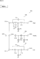
- FIG. 1 is a circuit configuration diagram of the filter according to the first embodiment.
- FIG. 2A is a diagram for explaining the principle of the present invention.
- FIG. 2B is a diagram for explaining the principle of the present invention.
- FIG. 3A is a diagram for explaining the principle of the present invention.
- FIG. 3B is a diagram for explaining the principle of the present invention.
- FIG. 4A is a diagram for explaining the principle of the present invention.
- FIG. 4B is a diagram for explaining the principle of the present invention.
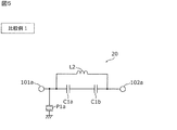
- FIG. 5 is a circuit configuration diagram of the filter according to Comparative Example 1.
- FIG. 6 is a graph comparing the pass characteristics of the filter according to the first embodiment and the pass characteristics of the filter according to the first comparative example.
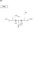
- FIG. 7 is a circuit configuration diagram of a filter according to Comparative Example 2.
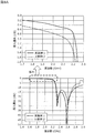
- FIG. 8A is a graph showing a comparison between the pass characteristics of the filter (low-pass filter) according to the first embodiment and the pass characteristics of the filter (low-pass filter) according to Comparative Example 2.
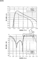
- FIG. 8B is a graph showing a comparison between the pass characteristic of the filter (high-pass filter) according to the first embodiment and the pass characteristic of the filter (high-pass filter) according to the second comparative example.
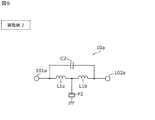
- FIG. 9 is a circuit configuration diagram of the filter according to the second embodiment.
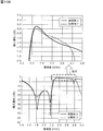
- FIG. 10A is a graph comparing the pass characteristics of the filter (low-pass filter) according to the second embodiment and the pass characteristics of the filter (low-pass filter) according to the second comparative example.
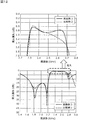
- FIG. 10B is a graph showing a comparison between the pass characteristics of the filter (high-pass filter) according to the second embodiment and the pass characteristics of the filter (high-pass filter) according to the second comparative example.
- FIG. 11 is a circuit configuration diagram of the filter according to the third embodiment.
- FIG. 12 is a graph showing a comparison between the pass characteristic of the filter according to the third embodiment and the pass characteristic of the filter according to the second comparative example.
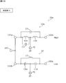
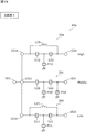
- FIG. 13 is a circuit configuration diagram of the multiplexer according to the fourth embodiment.
- FIG. 14 is a circuit configuration diagram of a multiplexer according to Comparative Example 3.
- FIG. 15 is a graph comparing the pass characteristics of the multiplexer according to the fourth embodiment and the pass characteristics of the multiplexer according to the third comparative example.
- FIG. 16 is a circuit configuration diagram of the multiplexer according to the fifth embodiment.
- FIG. 17 is a graph comparing the pass characteristics of the multiplexer according to the fifth embodiment and the pass characteristics of the multiplexer according to the third comparative example.
- FIG. 18 is a circuit configuration diagram of the multiplexer according to the sixth embodiment.
- FIG. 19 is a circuit configuration diagram of a multiplexer according to Comparative Example 4.
- FIG. 20 is a graph comparing the pass characteristics of the multiplexer according to the sixth embodiment and the pass characteristics of the multiplexer according to the fourth comparative example.
- FIG. 21 is a circuit configuration diagram of the multiplexer according to the seventh embodiment.
- FIG. 22 is a graph illustrating pass characteristics of the multiplexer according to the seventh embodiment.
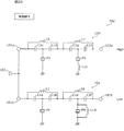
- FIG. 23 is a circuit configuration diagram of the multiplexer according to the eighth embodiment.
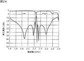
- FIG. 24 is a graph illustrating pass characteristics of the multiplexer according to the eighth embodiment.
- FIG. 25 is a circuit configuration diagram of the multiplexer according to the ninth embodiment.
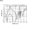
- FIG. 26 is a graph illustrating pass characteristics of the multiplexer according to the ninth embodiment.
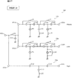
- FIG. 27 is a circuit configuration diagram of the multiplexer according to the tenth embodiment.
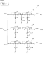
- FIG. 28 is a circuit configuration diagram of the multiplexer according to the eleventh embodiment.
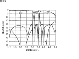
- FIG. 29 is a graph illustrating pass characteristics of the multiplexer according to the eleventh embodiment.
- FIG. 30 is a diagram for explaining the reason that each resonator constituting the multiplexer according to the fourth embodiment can be formed with one chip.
- FIG. 30 is a diagram for explaining the reason that each resonator constituting the multiplexer according to the fourth embodiment can be formed with one chip.
- FIG. 31 is a diagram for explaining the reason that each resonator forming the multiplexer according to the sixth embodiment can be formed by one chip.
- FIG. 32 is a top view schematically illustrating the structure of the multiplexer according to the sixth embodiment.
- FIG. 33 is a circuit configuration diagram of a filter according to a modification of the first embodiment.
- FIG. 34 is a graph illustrating pass characteristics of the filter according to the modification of the first embodiment when the switch is off and on.
- FIG. 35 is a circuit configuration diagram of the high-frequency front-end circuit according to the second embodiment.
- FIG. 36 is a circuit configuration diagram of the communication device according to the second embodiment.
- the high frequency filter is also referred to as a filter.
- the filter according to the first embodiment includes two first impedance elements connected in series on a path connecting the input terminal and the output terminal, and a second second impedance element connected in parallel to a series circuit of the two first impedance elements.
- the first impedance element is one of a capacitor and an inductor
- the second impedance element is the other of a capacitor and an inductor. That is, when the first impedance element is a capacitor, the second impedance element is an inductor, and when the first impedance element is an inductor, the second impedance element is a capacitor.
- an LC resonance circuit (specifically, an LC parallel resonance circuit) is configured by the two first impedance elements and the second impedance element. Further, the LC resonance circuit can function as both a high-pass filter and a low-pass filter by appropriately setting the respective element values (capacitance value, inductance value) of the two first impedance elements and the second impedance element. .
- the capacitor according to the present invention is an element that exhibits capacitance in all bands as an ideal element, and does not include an elastic wave resonator. This is because the elastic wave resonator exhibits inductive properties in a band between the resonance frequency and the anti-resonance frequency, and exhibits capacitive properties in other bands, but is not an element exhibiting capacitive properties in all bands.
- FIG. 1 is a circuit configuration diagram of the filter 10 according to the first embodiment.
- the filter 10 includes capacitors C1a and C1b, an inductor L2, and a parallel arm resonator P1.
- the capacitors C1a and C1b are two first impedance elements connected in series on a path connecting the terminal 101a and the terminal 102a.
- the terminal 101a is described as an input terminal, and the terminal 102a is described as an output terminal.
- the terminal 101a may be an output terminal, or the terminal 102a may be an input terminal.
- the inductor L2 is a second impedance element connected in parallel to a series circuit of the capacitors C1a and C1b. Specifically, the inductor L2 is connected between a connection point between the capacitor C1a and the terminal 101a and a connection point between the capacitor C1b and the terminal 102a.
- the LC resonance circuit 11 is formed by the capacitors C1a and C1b and the inductor L2.
- an LC resonance circuit is formed by two first impedance elements, one of the capacitor and the inductor, and a second impedance element, the other of the capacitor and the inductor.
- the dashed lines surrounding these and the description of “LC resonance circuit” are omitted.
- the parallel arm resonator P1 is an elastic wave resonator connected between the node N on the path connecting the terminal 101a and the terminal 102a between the capacitors C1a and C1b and the ground.
- the elastic wave resonator is a resonator using an elastic wave, for example, a resonator using SAW (Surface Acoustic Wave), a resonator using a BAW (Bulk Acoustic Wave), or an FBAR (Film Bulk Acoustic Resonator). ).
- SAW Surface Acoustic Wave
- BAW Bulk Acoustic Wave
- FBAR Fanm Bulk Acoustic Resonator
- SAW Surface Acoustic Wave
- the elastic wave resonator is a SAW resonator.
- the elastic wave resonator constituting the filter 10 can be constituted by an IDT (Inter Digital Transducer) electrode formed on a substrate having piezoelectricity, a small and low-profile filter circuit having high steep attenuation characteristics. Can be realized.
- IDT Inter Digital Transducer
- the substrate having piezoelectricity is a substrate having piezoelectricity on at least the surface.
- the substrate may include, for example, a piezoelectric thin film on the surface, a film having a different sound speed from the piezoelectric thin film, and a laminate such as a support substrate.
- the substrate is, for example, a high-sonic support substrate, a laminate including a piezoelectric thin film formed on the high-sonic support substrate, a high-sonic support substrate, and a low-sonic film formed on the high-sonic support substrate.
- a laminate including a piezoelectric thin film formed on a low-sonic film, or a supporting substrate, a high-sonic film formed on the supporting substrate, a low-sonic film formed on the high-sonic film, and a low-sonic It may be a laminate including a piezoelectric thin film formed on the film.
- the substrate may have piezoelectricity over the entire substrate. The same applies to the elastic wave resonators (series arm resonators and parallel arm resonators) described in the second to sixth embodiments, and the description is omitted in the second to sixth embodiments.
- a parallel arm resonator P1 is connected between capacitors C1a and C1b (two first impedance elements) constituting the LC resonance circuit 11, as shown in FIG. The principle of this will be described with reference to FIGS. 2A to 4B.
- [principle] 2A to 4B are views for explaining the principle of the present invention.
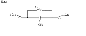
- FIG. 2A is a diagram illustrating a filter (LC resonance circuit) including the capacitor C1b and the inductor L2, in which the capacitor C1a and the parallel arm resonator P1 are removed from the configuration of the filter 10.
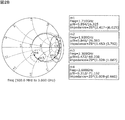
- FIG. 2B is a Smith chart showing the impedance characteristics of the filter shown in FIG. 2A.
- the Smith charts showing the impedance characteristics described in FIG. 2B, FIG. 3B and FIG. 4B show the vicinity of the lower end and the upper end of the required pass band, and the vicinity of the lower end of the required attenuation band. And a marker is added near the high frequency end.
- the frequency, the magnitude ⁇ and the phase ⁇ of the reflection coefficient, and the impedance (*) at the marker m * (where * is a numerical value following m in the graph) in the graph are shown.
- the coefficient Z0 is, for example, 50 ⁇ ).
- the required pass band is from 2300 MHz (frequency at marker m3) to 2690 MHz (frequency at marker m4)
- the required attenuation band is from 1710 MHz (frequency at marker m1) to 1920 MHz (frequency at marker m2).
- the filter shown in FIG. 2A is, for example, a high-pass filter in order to realize the required pass band and attenuation band, and as shown in FIG. 2B, near the low end and high end of the pass band. Is close to 50 ⁇ , and the impedance near the low end and high end of the attenuation band is almost open.
- the vicinity of the low end and the vicinity of the high end (markers m3 and m4) of the pass band are surrounded by broken-line circles, and the vicinity of the low end and high end of the attenuation band (markers m1 and m2). ) Is surrounded by a dot-dash line circle.
- the filter shown in FIG. 2A is an LC resonance circuit including the capacitor C1b and the inductor L2, it is difficult to obtain steep attenuation characteristics. On the other hand, it is conceivable to obtain a steep damping characteristic by adding an elastic wave resonator having a steep damping pole.
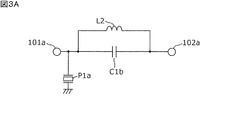
- FIG. 3A is a diagram in which a parallel arm resonator P1a is added to the configuration of the filter shown in FIG. 2A, and shows a filter including a capacitor C1b, an inductor L2, and a parallel arm resonator P1a.
- the parallel arm resonator P1a is connected between the node between the connection point of the capacitor C1b and the inductor L2 connected in parallel and the terminal 101a, and the ground.
- the parallel arm resonator P1a is a resonator having a resonance frequency of 2200 MHz and an anti-resonance frequency of 2500 MHz. Therefore, the parallel arm resonator P1a shows inductive properties in the resonance bandwidth (2200 MHz to 2500 MHz) and shows capacitive properties in other bands.
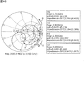
- FIG. 3B is a Smith chart showing the impedance characteristics of the filter shown in FIG. 3A.
- FIG. 3B shows a dot-dash line circle at the same position as the markers m1 and m2 shown in FIG. 2B. 2B, the same positions as the markers m3 and m4 are indicated by broken-line circles.
- the position of the marker m3 is shifted from the position of the dashed circle by adding the parallel arm resonator P1a exhibiting inductive properties at the frequency. Rotate clockwise (direction of arrow A).
- the frequency at the marker m4 near the high-frequency end of the passband is 2690 MHz
- the position of the marker m4 is indicated by a broken-line circle due to the addition of the parallel arm resonator P1a showing the capacitance at the frequency. Rotate clockwise from the position (direction of arrow B).
- the pass band from 2300 MHz to 2690 MHz, from the center (50 ⁇ ) of the Smith chart, The separated bands increase, and the insertion loss in the pass band increases.
- the parallel arm resonator P1a showing the capacitance at these frequencies is As a result of the addition, the positions of the markers m1 and m2 rotate in the clockwise direction (the direction of arrow C) from the position of the dashed-dotted circle. As described above, the attenuation band from 1710 MHz to 1920 MHz is apart from the open position of the Smith chart, and the attenuation characteristic is deteriorated.
- FIG. 4A is a diagram showing a filter in which a capacitor C1a is connected in series to a capacitor C1b in the configuration of the filter shown in FIG. 2A, and a parallel arm resonator P1 is connected between a node between the capacitors C1a and C1b and ground. is there.
- FIG. 4B is a Smith chart showing the impedance characteristics of the filter shown in FIG. 4A.
- FIG. 9 is a graph showing a change in impedance characteristics due to the addition of the capacitor C1a and the parallel arm resonator P1 to the filter shown in FIG. 2A (specifically, the addition of the capacitor C1a and the parallel arm resonator P1 in this order).
- a dashed-dotted circle is provided at the same position as the markers m1 and m2 shown in FIG. 2B, and a dashed-dotted circle is provided at the same position as the markers m3 and m4 shown in FIG.
- the parallel arm resonator P1 is a resonator having a resonance frequency of 2200 MHz and an anti-resonance frequency of 2500 MHz, like the parallel arm resonator P1a. For this reason, the parallel arm resonator P1 shows inductive properties in the resonance bandwidth (2200 MHz to 2500 MHz) and shows capacitive properties in other bands.
- the position of each marker rotates in the counterclockwise direction because the capacitor C1a showing the capacitance in all bands is connected in series to the capacitor C1b.
- the positions of the markers m3 and m4 rotate in the direction of arrow A from the position of the dashed circle and move to the vicinity of the position of the two-dot chain line circle.
- the positions of the markers m1 and m2 rotate in the direction of arrow B from the position of the dot-dash line circle. Note that the positions of the markers m1 and m2 are originally near the open position, and do not move greatly on the Smith chart even if the capacitor C1a is added. It is not shown like a two-dot chain line circle.
- the position of the marker m3 is changed to the position indicated by the two-dot chain line circle due to the addition of the parallel arm resonator P1 exhibiting inductive properties at the frequency. From the counterclockwise direction (direction of arrow C).
- the frequency at the marker m4 near the high-frequency end of the passband is 2690 MHz
- the position of the marker m4 is indicated by the two-dot chain line due to the addition of the parallel arm resonator P1 showing the capacitance at the frequency. It rotates clockwise (direction of arrow D) from the position of the circle.
- the positions of the markers m3 and m4 which were within the dashed circle were once rotated in the direction of arrow A by the capacitor C1a. It is considered that by rotating the markers m3 and m4 by P1, it was possible to approach the center of the Smith chart. Therefore, an increase in insertion loss in the pass band can be suppressed.
- the capacitance value of the capacitor C1a (that is, rotation in the direction of arrow A) is set so that the impedance at the markers m3 and m4 (that is, in the pass band) after the addition of the parallel arm resonator P1 is located near the center of the Smith chart. Volume) has been adjusted.
- the frequency of the marker m1 near the lower end of the attenuation band is 1710 MHz
- the frequency of the marker m2 near the higher end is 1920 MHz.
- the positions of the markers m1 and m2 rotate in the clockwise direction (the direction of arrow E) from the position of the dashed-dotted circle.
- the positions of the markers m1 and m2 which were within the dashed-dotted circle were once rotated in the direction of arrow B by the capacitor C1a. Even if m2 and m2 are rotated in the direction of arrow E, the Smith chart can be kept away from the open position. Therefore, the deterioration of the attenuation characteristic can be suppressed.
- FIG. 5 is a circuit configuration diagram of the filter 20 according to Comparative Example 1.
- the filter 20 according to Comparative Example 1 is different from the filter 10 according to Example 1 in the position where the parallel arm resonator is connected.
- the other points are the same as those in the filter 10, and the description is omitted.
- the parallel arm resonator P1a is connected between the ground between a node between the LC resonance circuit including the capacitors C1a and C1b and the inductor L2 and the terminal 101a and the ground. That is, in the filter 20, the parallel arm resonator P1a is not connected between the capacitors C1a and C1b as in the first embodiment, and has a configuration similar to that of the filter illustrated in FIG. 3A.
- FIG. 6 is a graph showing a comparison between the pass characteristic of the filter 10 according to the first embodiment and the pass characteristic of the filter 20 according to the first comparative example.
- the graph shown on the upper side of FIG. 6 is an enlarged view around the broken line circle of the graph shown on the lower side. It should be noted that the same applies to the subsequent diagrams showing the passing characteristics, in which the dashed circle indicates “enlarged”.
- the solid line indicates the pass characteristic of the filter 10 according to the first embodiment
- the broken line indicates the pass characteristic of the filter 20 according to the first comparative example.
- FIG. 6 is a graph showing pass characteristics when the filters 10 and 20 are designed to function as high-pass filters.
- the filters 10 and 20 include an elastic wave resonator, and both have steep attenuation characteristics as shown in FIG. 6 due to the steep attenuation pole caused by the elastic wave resonator.
- the filter 10 can suppress an increase in insertion loss in the pass band (2300 MHz to 2690 MHz) as compared with the filter 20.
- the insertion loss at 2300 MHz is 1.191 dB for the filter 20, while the filter 10 is as small as 0.838 dB for the filter 20, and the insertion loss at 2690 MHz is 4.216 dB for the filter 20.
- the filter 10 is as small as 1.391 dB.
- FIG. 7 is a circuit configuration diagram of the filter 20a according to Comparative Example 2.
- the filter 20a according to Comparative Example 2 includes the series arm resonators S10 and S20, the inductor L20, and the parallel arm resonator P10.
- the series arm resonators S10 and S20 are connected in series on a path connecting the terminal 101a and the terminal 102a.
- the inductor L20 is connected in parallel to the series circuit of the series arm resonators S10 and S20. Specifically, the inductor L20 is connected between a connection point between the series arm resonator S10 and the terminal 101a and a connection point between the series arm resonator S20 and the terminal 102a.
- the parallel arm resonator P10 is an elastic wave resonator connected between a node on the path connecting the terminal 101a and the terminal 102a between the series arm resonators S10 and S20 and the ground.
- the filter 20a according to the comparative example 2 is a ladder-type filter in which the series arm resonators S10 and S20 are connected instead of the two capacitors C1a and C1b, and the elastic wave resonators are arranged in a ladder-type. 1 is different from the filter 10 according to the first embodiment. Note that the element parameters of the series arm resonators S10 and S20, the inductor L20, and the parallel arm resonator P10 are adjusted such that the filter 20a has a pass band equivalent to that of the filter 10.
- the elastic wave resonator exhibits a capacitive characteristic in a band other than between the resonance frequency and the anti-resonance frequency, and can be used as a substitute for a capacitor. That is, it is considered that the function of the filter 10 according to the first embodiment can also be realized by the filter 20a according to the second comparative example.
- the pass band of the ladder-type filter is limited by the resonance bandwidth of each elastic wave resonator. Therefore, by giving Comparative Example 2 as a comparative object of Example 1, it is possible to confirm how excellent the pass characteristic of the filter of the present invention is compared with the ladder type filter.
- FIG. 8A is a graph showing a comparison between pass characteristics of the filter 10 (low-pass filter) according to the first embodiment and pass characteristics of the filter 20a (low-pass filter) according to the second comparative example.
- the solid line indicates the pass characteristic of the filter 10 according to the first embodiment
- the broken line indicates the pass characteristic of the filter 20a according to the second comparative example.
- the filter 10 and the filter 20a include an elastic wave resonator, and both have a steep attenuation characteristic as shown in FIG. 8A due to a steep attenuation pole caused by the elastic wave resonator.
- the filter 10 can suppress an increase in insertion loss in the pass band as compared with the filter 20a. Specifically, the insertion loss at 2200 MHz is as small as 0.792 dB for the filter 10 while the filter 20a is 1.561 dB for the filter 20a.
- FIG. 8B is a graph comparing the pass characteristics of the filter 10 (high-pass filter) according to the first embodiment and the pass characteristics of the filter 20a (high-pass filter) according to the second comparative example.
- the solid line indicates the pass characteristic of the filter 10 according to the first embodiment
- the broken line indicates the pass characteristic of the filter 20a according to the second comparative example.
- the filter 10 and the filter 20a each include an elastic wave resonator, and both have steep attenuation characteristics as shown in FIG. 8B due to the steep attenuation pole of the elastic wave resonator.
- the filter 10 can suppress an increase in insertion loss in the pass band (2300 MHz to 2690 MHz) as compared with the filter 20a. Specifically, the insertion loss at 2300 MHz is 0.94 dB for the filter 20a, whereas the filter 10 is as small as 0.922 dB for the filter 20a, and the insertion loss at 2690 MHz is 1.483 dB for the filter 20a. On the other hand, the filter 10 is as small as 1.1 dB.
- the ladder-type filter using the elastic wave resonator instead of the capacitors C1a and C1b has deteriorated transmission characteristics. That is, when the LC resonance circuit is configured as in the present invention, the deterioration of the transmission characteristic can be suppressed by not using the elastic wave resonator instead of the capacitor.
- the filter 10 having a steep attenuation characteristic and having a low-loss passband which is not limited to the resonance bandwidth (for example, 300 MHz or the like) of the elastic wave resonator like a ladder filter. .
- FIG. 9 is a circuit configuration diagram of the filter 10a according to the second embodiment.
- the filter 10a includes inductors L1a and L1b, a capacitor C2, and a parallel arm resonator P2.
- the inductors L1a and L1b are two first impedance elements connected in series on a path connecting the terminal 101a and the terminal 102a.
- the capacitor C2 is a second impedance element connected in parallel to a series circuit of the inductors L1a and L1b. Specifically, the capacitor C2 is connected between a connection point between the inductor L1a and the terminal 101a and a connection point between the inductor L1b and the terminal 102a.
- the second embodiment differs from the first embodiment in that the two first impedance elements are inductors and the second impedance element is a capacitor.
- an LC resonance circuit is formed by the inductors L1a and L1b and the capacitor C2.
- the parallel arm resonator P2 is an elastic wave resonator connected between a node on a path connecting the terminals 101a and 102a between the inductors L1a and L1b and the ground.
- FIG. 10A is a graph showing a comparison between the pass characteristic of the filter 10a (low-pass filter) according to the second embodiment and the pass characteristic of the filter 20a (low-pass filter) according to the second comparative example.
- the solid line indicates the pass characteristic of the filter 10a according to the second embodiment
- the broken line indicates the pass characteristic of the filter 20a according to the second comparative example.
- the filters 10a and 20a each include an elastic wave resonator, and both have steep attenuation characteristics as shown in FIG. 10A due to the steep attenuation pole caused by the elastic wave resonator.
- the filter 10a can suppress an increase in insertion loss in the pass band as compared with the filter 20a.
- the insertion loss at 2200 MHz is 1.561 dB for the filter 20a, and 0.825 dB for the filter 10a.
- FIG. 10B is a graph showing a comparison between the pass characteristic of the filter 10a (high-pass filter) according to the second embodiment and the pass characteristic of the filter 20a (high-pass filter) according to the second comparative example.
- the solid line indicates the pass characteristic of the filter 10a according to the second embodiment
- the broken line indicates the pass characteristic of the filter 20a according to the second comparative example.
- the filters 10a and 20a each include an elastic wave resonator, and as shown in FIG. 10B, both have steep attenuation characteristics due to a steep attenuation pole of the elastic wave resonator.
- the filter 10a can suppress an increase in insertion loss in a pass band (2300 MHz to 2690 MHz) as compared with the filter 20a. Specifically, the insertion loss at 2300 MHz is 0.94 dB for the filter 20a, whereas the filter 10a is as small as 0.838 dB, and the insertion loss at 2690 MHz is 1.483 dB for the filter 20a. On the other hand, the filter 10a is as small as 1.391 dB.
- the filter 10a having a steep attenuation characteristic and having a low-loss passband.
- FIG. 11 is a circuit configuration diagram of the filter 10b according to the third embodiment.
- the filters according to the first and second embodiments may further include a third impedance element connected in parallel to one of the two first impedance elements.
- the third impedance element is a capacitor.
- the third impedance element is an inductor.
- a filter in which the first impedance element is an inductor and the third impedance element is a capacitor specifically, a capacitor C3 is connected in parallel to the inductor L1a (first impedance element) in the second embodiment.
- the filter 10b will be described.
- the filter 10b includes a capacitor C3 in addition to the configuration of the filter 10a according to the second embodiment.
- the other points are the same as those in the second embodiment, and the description is omitted.
- the capacitor C3 is connected in parallel with the inductor L1a. Note that the capacitor C3 may be connected in parallel with the inductor L1b instead of the inductor L1a.
- FIG. 12 is a graph showing a comparison between the pass characteristic of the filter 10b according to the third embodiment and the pass characteristic of the filter 20a according to the second comparative example.
- the solid line indicates the pass characteristic of the filter 10b according to the third embodiment
- the broken line indicates the pass characteristic of the filter 20a according to the second comparative example.
- FIG. 12 is a graph showing pass characteristics when the filters 10b and 20a are designed to function as high-pass filters.
- the filters 10b and 20a include elastic wave resonators, and both have steep attenuation characteristics as shown in FIG. 12 due to the steep attenuation pole of the elastic wave resonator.
- the filter 10b can suppress an increase in the insertion loss in the pass band (2300 MHz to 2690 MHz) as compared with the filter 20a.
- the insertion loss at 2300 MHz is 0.94 dB for the filter 20a
- the filter 10a is as small as 0.907 dB
- the insertion loss at 2690 MHz is 1.483 dB for the filter 20a.
- the filter 10a is as small as 1.314 dB.
- the provision of the capacitor C3 makes it possible to make the impedance close to 50 ⁇ near the high-frequency end of the pass band. Therefore, at 2690 MHz, the insertion loss can be made smaller than in the second embodiment. .
- the filter 10b having a steep attenuation characteristic and having a low-loss passband.
- the capacitor C1a has a steep attenuation characteristic and a low loss. Filter 10 having a wide pass band can be realized.
- the filters according to the first to third embodiments described above can be applied to a multiplexer. Such a multiplexer will be described as Examples 4 to 11.
- the multiplexers according to the fourth to eleventh embodiments specifically include a plurality of filters each including the filters according to the first to third embodiments.
- the multiplexer includes a filter other than a plurality of filters (a third filter in the sixth embodiment, a low-pass filter in the ninth embodiment, and a high-pass filter in the tenth embodiment). ) In some cases. Input terminals or output terminals of the plurality of filters are connected to a common terminal.
- the plurality of filters include at least a first filter and a second filter, and an input terminal or an output terminal of the first filter and an input terminal or an output terminal of the second filter are connected to a common terminal.
- the input terminals of the plurality of filters are connected to the common terminal, but the output terminals may be connected to the common terminal.
- the multiplexer includes filters other than the plurality of filters, input terminals or output terminals of the filters other than the plurality of filters are also connected to the common terminal.
- the multiplexers according to the fourth to eleventh embodiments simultaneously output signals in a plurality of frequency bands respectively corresponding to filters constituting the multiplexer (a filter having an input terminal or an output terminal connected to a common terminal in the multiplexer). Transmission and reception, that is, so-called CA may be supported.
- the plurality of frequency bands corresponding to each of the filters constituting the multiplexer may be, for example, an LTE (Long Term Evolution: 4G) Band or an NR (New Radio: 5G) Band. Good.
- the plurality of frequency bands are, for example, sub @ 6 GHz (n77 (3.3-4.2 GHz), n78 (3.3-3.8 GHz), n79 (4.4-5.0 GHz) as NR Bands. ), 5.0-7.125 GHz).
- Band of 5.0-7.125 GHz for example, Band 46 (5150-5925 MHz) or Band 47 (5855-5925 MHz) is used.
- the plurality of frequency bands may be, for example, L5 of Global Positioning System (GPS).
- GPS Global Positioning System
- the plurality of frequency bands may include a 5 GHz band of Wi-Fi (registered trademark).
- the 5 GHz band may be, for example, 5150-5725 MHz.
- the first filter and the second filter may be filters that include any of these frequency bands in a pass band.
- the multiplexer includes a filter including a pass band of 699 MHz to 960 MHz, a filter including a pass band of 1.2 GHz, a filter including a pass band of 1.4 GHz to 5 GHz, and a pass band of 5 GHz to 7.125 GHz. And at least two filters. Further, for example, the multiplexer includes a filter including a pass band of 699 MHz to 2.7 GHz, a filter including a pass band of 3.3 GHz to 4.2 GHz, a filter including a pass band of 4.4 GHz to 5 GHz, and a filter including a pass band of 4.4 GHz to 5 GHz. At least two filters may be included among filters having a pass band of 7.125 GHz.
- FIG. 13 is a circuit configuration diagram of the multiplexer 30 according to the fourth embodiment.
- the plurality of filters in the multiplexer 30 include the first filter and the second filter as the filters according to the first to third embodiments.
- the multiplexer 30 is a diplexer including two filters according to the first embodiment.
- the two filters according to the first embodiment are filters 10 and 10d.
- the filter 10d is a first filter
- the filter 10 is a second filter.
- the filter 10d includes capacitors C1c and C1d, an inductor L5, and a parallel arm resonator P3.
- the capacitors C1c and C1d are two first impedance elements connected in series on a path connecting the terminal 101a and the terminal 102a.
- the inductor L5 is a second impedance element connected in parallel to a series circuit of the capacitors C1c and C1d. Specifically, the inductor L5 is connected between a connection point between the capacitor C1c and the terminal 101a and a connection point between the capacitor C1d and the terminal 102a.
- the parallel arm resonator P3 is an elastic wave resonator connected between the ground and a node on a path connecting the terminals 101a and 102a between the capacitors C1c and C1d.
- the filter 10d has the same configuration as the filter 10 of the first embodiment.
- the first impedance element included in the filter 10d and the first impedance element included in the filter 10 are both capacitors.
- the terminal 101b is, for example, an input terminal, and the terminal 102b is, for example, an output terminal.
- the input terminal (terminal 101a) of the filter 10d and the input terminal (terminal 101b) of the filter 10 are commonly connected to the common terminal 103.
- the common terminal 103 and the terminals 101a and 101b may be directly connected without interposing any other element or the like, or may be indirectly connected with another element.
- the filter 10d is a high-pass filter
- the filter 10 is a low-pass filter
- the pass band of the filter 10d is higher than the pass band of the filter 10.
- the multiplexer 30 can support two frequency bands. In FIG. 13, “High” is described next to the terminal 102 a of the filter 10 d and “Low” is described next to the terminal 102 b of the filter 10 because the pass band of the filter 10 d It is higher than the band.
- FIG. 14 is a circuit configuration diagram of the multiplexer 40 according to Comparative Example 3.
- the multiplexer 40 is a diplexer including two filters according to Comparative Example 2.
- the two filters according to Comparative Example 2 are filters 20a and 20b.
- the configuration of the filter 20b is the same as that of the filter 20a, the description is omitted.
- the filter 20a is a high-pass filter
- the filter 20b is a low-pass filter.
- the pass band of the filter 20a is higher than the pass band of the filter 20b.
- "High” is described next to the terminal 102a of the filter 20a
- "Low” is described next to the terminal 102b of the filter 20b because the pass band of the filter 20a is higher than that of the filter 20b. It is higher than the band.
- the element values of the filter 20a are set so that the filter 20a has the same pass band as the filter 10d
- the element values of the filter 20b are set so that the filter 20b has the same pass band as the filter 10. Have been.
- FIG. 15 is a graph comparing the pass characteristics of the multiplexer 30 according to the fourth embodiment and the pass characteristics of the multiplexer 40 according to the third comparative example.
- the solid line indicates the pass characteristic of the multiplexer 30 according to the fourth embodiment
- the broken line indicates the pass characteristic of the multiplexer 40 according to the third comparative example.
- “High” is described in the pass band formed by the filter 10 d configuring the multiplexer 30 and the filter 20 a configuring the multiplexer 40.
- “Low” is described in a pass band formed by the filter 10 forming the multiplexer 30 and the filter 20 b forming the multiplexer 40.
- Each of the filters 10d and 20a includes an elastic wave resonator. Due to a steep attenuation pole caused by the elastic wave resonator, each of the multiplexers has a steep attenuation characteristic at the lower end of the pass band indicated by “High” in FIG. Have. Each of the filters 10 and 20b also includes an elastic wave resonator. Due to the steep attenuation pole caused by the elastic wave resonator, each of the multiplexers is steep at the high-frequency end of the pass band indicated by “Low” in FIG. It has attenuation characteristics. On the other hand, the multiplexer 30 can suppress an increase in insertion loss in the pass band as compared with the multiplexer 40.
- the insertion loss at 2200 MHz is 1.806 dB for the multiplexer 40 and 1.226 dB for the multiplexer 30.
- the insertion loss at 2300 MHz is 1.778 dB in the multiplexer 40
- the multiplexer 30 is as small as 1.217 dB.
- the insertion loss at 2690 MHz is 1.02 dB in the multiplexer 40.
- the multiplexer 30 is as small as 0.788 dB.
- the multiplexer 30 having steep attenuation characteristics and a low-loss passband can be realized.
- the first filter is the filter 10d (the filter according to the first embodiment), but the first filter may be the filter 10a (the filter according to the second embodiment).
- both the first impedance element included in the filter 10d (first filter) and the first impedance element included in the filter 10 (second filter) are capacitors, so that the first filter As compared with the case where the filter 10a is used, a multiplexer having a pass band with lower loss can be realized.
- the inductor has a lower Q value than the capacitor, and by using the filter 10d according to the first embodiment having a smaller number of inductors than the filter 10a according to the second embodiment, the total number of inductors having a low Q value used in the multiplexer is reduced. It is because it becomes less. In other words, the total number of capacitors having a high Q value is increased, and the loss can be reduced.
- FIG. 16 is a circuit configuration diagram of the multiplexer 30a according to the fifth embodiment.
- the multiplexer 30a includes a filter 10b instead of the filter 10d in the multiplexer 30 according to the fourth embodiment.
- the other points are the same as those in the fourth embodiment, and the description is omitted.
- the filter 10b is a high-pass filter
- the filter 10 is a low-pass filter
- the pass band of the filter 10b is higher than the pass band of the filter 10.
- the multiplexer 30a can support two frequency bands. In FIG. 16, “High” is described next to the terminal 102 a of the filter 10 b and “Low” is described next to the terminal 102 b of the filter 10 because the pass band of the filter 10 b It is higher than the band.
- FIG. 17 is a graph comparing the pass characteristics of the multiplexer 30a according to the fifth embodiment and the pass characteristics of the multiplexer 40 according to the third comparative example.
- the solid line indicates the pass characteristic of the multiplexer 30a according to the fifth embodiment
- the broken line indicates the pass characteristic of the multiplexer 40 according to the third comparative example.
- “High” is described in the pass band formed by the filter 10 b forming the multiplexer 30 a and the filter 20 a forming the multiplexer 40.
- “Low” is described in the pass band formed by the filter 10 forming the multiplexer 30a and the filter 20b forming the multiplexer 40.
- Each of the filters 10b and 20a includes an elastic wave resonator. Due to a steep attenuation pole caused by the elastic wave resonator, each of the multiplexers has a steep attenuation characteristic at a lower end of a pass band indicated by “High” in FIG. Have. Each of the filters 10 and 20b also includes an elastic wave resonator. Due to a steep attenuation pole caused by the elastic wave resonator, each of the multiplexers is steep at the high-frequency end of the pass band indicated by “Low” in FIG. It has attenuation characteristics. On the other hand, the multiplexer 30a can suppress an increase in insertion loss in the pass band as compared with the multiplexer 40.
- the insertion loss at 2200 MHz is 1.806 dB for the multiplexer 40 and 1.05 dB for the multiplexer 30a.
- the multiplexer 30 has an insertion loss of 1.778 dB at 2300 MHz, the multiplexer 30 has a low insertion loss of 1.074 dB, and the insertion loss at 2690 MHz has a multiplexer of 1.02 dB.
- the multiplexer 30 is as small as 0.897 dB.
- the multiplexer 30a having a steep attenuation characteristic and having a low-loss passband.
- FIG. 18 is a circuit configuration diagram of the multiplexer 30b according to the sixth embodiment.
- the plurality of filters in the multiplexer 30b include a first filter and a second filter as the filters according to the first to third embodiments. Further, the multiplexer 30b further includes a third filter whose input terminal or output terminal is connected to the common terminal. The third filter includes at least one series arm resonator and at least one parallel arm resonator. Specifically, the multiplexer 30b is a triplexer including the filter 10 according to the first embodiment, the filter 10b according to the third embodiment, and the filter 20c. For example, the filter 10b is a first filter, the filter 10 is a second filter, and the filter 20c is a third filter.
- the terminal 101c is, for example, an input terminal
- the terminal 102c is, for example, an output terminal.
- the input terminal (terminal 101a) of the filter 10b, the input terminal (terminal 101c) of the filter 20c, and the input terminal (terminal 101b) of the filter 10 are commonly connected to the common terminal 103.
- the common terminal 103 and the terminals 101a, 101b, and 101c may be directly connected without interposing any other element or the like, or may be indirectly connected through another element. Good.
- the filter 10b is a high-pass filter
- the filter 10 is a low-pass filter
- the filter 20c is a band-pass filter.
- the pass band of the filter 10b is higher than the pass band of the filter 10
- the pass band of the filter 20c is lower than the pass band of the filter 10b and higher than the pass band of the filter 10.
- the multiplexer 30b can support three frequency bands.
- “High” is described next to the terminal 102a of the filter 10b
- “Middle” is described next to the terminal 102c of the filter 20c
- “Low” is described next to the terminal 102b of the filter 10.
- the pass band of the filter 10b is higher than the pass band of the filter 20c
- the pass band of the filter 20c is higher than the pass band of the filter 10.
- the filter 20c includes the series arm resonators S30 and S40 as at least one series arm resonator, and the parallel arm resonators P20 and P30 as at least one parallel arm resonator.
- Series arm resonators S30 and S40 are connected in series on a path connecting terminal 101c and terminal 102c.
- the parallel arm resonator P20 is connected between the node between the series arm resonator S30 and the series arm resonator S40 and the ground
- the parallel arm resonator P30 is connected between the series arm resonator S40 and the terminal 102c. Is connected between this node and the ground.
- the filter 20c may include one or three or more series arm resonators as at least one series arm resonator, and one or three or more parallel arm resonances as at least one parallel arm resonator. A child may be provided.
- FIG. 19 is a circuit configuration diagram of the multiplexer 40a according to Comparative Example 4.
- the multiplexer 40a is a triplexer including the two filters according to the comparative example 2 and the filter 20c.
- two filters according to Comparative Example 2 are filters 20a and 20b.
- the filter 20c in Comparative Example 4 is the same as that in Example 6.
- the filter 20a is a high-pass filter
- the filter 20b is a low-pass filter
- the filter 20c is a band-pass filter.
- the pass band of the filter 20a is higher than the pass band of the filter 20b
- the pass band of the filter 20c is lower than the pass band of the filter 20a and higher than the pass band of the filter 20b.
- “High” is described next to the terminal 102a of the filter 20a
- “Middle” is described next to the terminal 102c of the filter 20c
- “Low” is described next to the terminal 102b of the filter 20b.
- the pass band of the filter 20a is higher than the pass band of the filter 20c, and the pass band of the filter 20c is higher than the pass band of the filter 20b.
- the element values of the filter 20a are set so that the filter 20a has a pass band equivalent to the filter 10b, and the element values of the filter 20b are set so that the filter 20b has a pass band equivalent to the filter 10. Have been.
- FIG. 20 is a graph showing a comparison between the pass characteristics of the multiplexer 30b according to the sixth embodiment and the pass characteristics of the multiplexer 40a according to the fourth comparative example.
- the solid line indicates the pass characteristic of the multiplexer 30b according to the sixth embodiment
- the dashed line indicates the pass characteristic of the multiplexer 40a according to the comparative example 4.
- “High” is described in the pass band formed by the filter 10b forming the multiplexer 30b and the filter 20a forming the multiplexer 40a.
- “Middle” is described in the passband formed by the filters 20c constituting the multiplexers 30b and 40a, respectively.
- “Low” is described in the pass band formed by the filter 10 forming the multiplexer 30b and the filter 20b forming the multiplexer 40a.
- Each of the filters 10b and 20a includes an elastic wave resonator. Due to a steep attenuation pole caused by the elastic wave resonator, each multiplexer has a steep attenuation characteristic at a lower end of a pass band indicated by "High” in FIG. Have. Also, the filters 10 and 20b also include an elastic wave resonator. Due to the steep attenuation pole caused by the elastic wave resonator, each multiplexer is steep at the high-frequency end of the pass band indicated by “Low” in FIG. It has attenuation characteristics. On the other hand, the multiplexer 30b can suppress an increase in insertion loss in the pass band as compared with the multiplexer 40a.
- the insertion loss at 2200 MHz is 1.488 dB for the multiplexer 40a and 1.15 dB for the multiplexer 30b.
- the insertion loss at 2500 MHz is as small as 1.074 dB for the multiplexer 30a, while it is 1.225 dB for the multiplexer 40a.
- the multiplexer 30b having a steep attenuation characteristic and having a low-loss passband.
- FIG. 21 is a circuit configuration diagram of the multiplexer 30c according to the seventh embodiment.
- the plurality of filters in the multiplexer 30c include a first filter and a second filter as filters combining the filters according to the first to third embodiments.
- the multiplexer 30c is a diplexer including filters 10e and 10f, and the filters 10e and 10f are filters obtained by combining the filters according to the first and second embodiments, respectively.
- the filter 10f is a first filter
- the filter 10e is a second filter.
- the filter 10e includes capacitors C1a, C1b, C2, inductors L1a, L1b, L10, L11, and parallel arm resonators P1 and P2.
- the capacitors C1a and C1b are two first impedance elements connected in series on a path connecting the terminal 101b and the terminal 102b.
- the inductor L1a is a second impedance element connected in parallel to a series circuit of the capacitors C1a and C1b. Specifically, the inductor L1a is connected between a connection point between the capacitor C1a and the terminal 101b and a connection point between the capacitor C1b and the inductor L1b.
- the parallel arm resonator P1 is an elastic wave resonator connected between a node on a path connecting the terminals 101b and 102b between the capacitors C1a and C1b and the ground.
- the inductor L10 is an inductor connected in series with the parallel arm resonator P1 between the node and the ground.
- the filter composed of the capacitors C1a and C1b, the inductor L1a, and the parallel arm resonator P1 in the filter 10e has the same configuration as the filter 10 of the first embodiment.
- the inductor L1a is also a first impedance element.
- the inductors L1a and L1b are connected in series on a path connecting the terminal 101b and the terminal 102b.
- the inductors L1a and L1b become first impedance elements. It is.
- the capacitor C2 is a second impedance element connected in parallel to a series circuit of the inductors L1a and L1b. Specifically, the capacitor C2 is connected between a connection point between the inductor L1a and the terminal 101b and a connection point between the inductor L1b and the terminal 102b.
- the parallel arm resonator P2 is an elastic wave resonator connected between the ground and a node on a path connecting the terminals 101b and 102b between the inductors L1a and L1b.
- the inductor L11 is an inductor connected in series with the parallel arm resonator P2 between the node and the ground.
- the filter composed of the inductors L1a and L1b, the capacitor C2 and the parallel arm resonator P2 in the filter 10e has the same configuration as the filter 10a of the second embodiment.
- the filter 10f includes capacitors C1c, C1d, and C4, inductors L1c, L1d, L12, and L13, and parallel arm resonators P3 and P4.
- the capacitors C1c and C1d are two first impedance elements connected in series on a path connecting the terminal 101a and the terminal 102a.
- the inductor L1c is a second impedance element connected in parallel to a series circuit of the capacitors C1c and C1d. Specifically, the inductor L1c is connected between a connection point between the capacitor C1c and the terminal 101a and a connection point between the capacitor C1d and the inductor L1d.
- the parallel arm resonator P3 is an elastic wave resonator connected between the ground and a node on a path connecting the terminals 101a and 102a between the capacitors C1c and C1d.
- the inductor L12 is an inductor connected in series with the parallel arm resonator P3 between the node and the ground.
- the filter composed of the capacitors C1c and C1d, the inductor L1c, and the parallel arm resonator P3 in the filter 10f has the same configuration as the filter 10 of the first embodiment.
- the inductor L1c is also a first impedance element.
- the inductors L1c and L1d are connected in series on a path connecting the terminal 101a and the terminal 102a.
- the inductors L1c and L1d become first impedance elements. It is.
- the capacitor C4 is a second impedance element connected in parallel to a series circuit of the inductors L1c and L1d. Specifically, the capacitor C4 is connected between a connection point between the inductor L1c and the terminal 101a and a connection point between the inductor L1d and the terminal 102a.
- the parallel arm resonator P4 is an elastic wave resonator connected between a ground and a node on a path connecting the terminals 101a and 102a between the inductors L1c and L1d.
- the inductor L13 is an inductor connected in series with the parallel arm resonator P4 between the node and the ground.
- the filter composed of the inductors L1c and L1d, the capacitor C4, and the parallel arm resonator P4 in the filter 10f has the same configuration as the filter 10a of the second embodiment.
- the input terminal (terminal 101a) of the filter 10f and the input terminal (terminal 101b) of the filter 10e are commonly connected to the common terminal 103.
- the common terminal 103 and the terminals 101a and 101b may be directly connected without interposing any other element or the like, or may be indirectly connected with another element.
- the filter 10f is a high-pass filter
- the filter 10e is a low-pass filter
- the pass band of the filter 10f is higher than the pass band of the filter 10e.
- the multiplexer 30c can support two frequency bands. In FIG. 21, “High” is described next to the terminal 102 a of the filter 10 f and “Low” is described next to the terminal 102 b of the filter 10 e because the pass band of the filter 10 f is higher than the pass band of the filter 10 e. It is higher than the band.
- FIG. 22 is a graph showing the pass characteristics of the multiplexer 30c according to the seventh embodiment.
- "High” is described in the pass band formed by the filter 10f included in the multiplexer 30c.
- “Low” is described in the pass band formed by the filter 10 e that configures the multiplexer 30 c.
- the filter 10f includes an elastic wave resonator, and the multiplexer 30c has a steep attenuation characteristic at the lower end of the pass band indicated by “High” in FIG. 22 due to the steep attenuation pole caused by the elastic wave resonator. I have. Further, the filter 10e also includes an elastic wave resonator, and the steep attenuation pole by the elastic wave resonator causes the multiplexer 30c to exhibit a steep attenuation characteristic at a high-frequency end of a pass band indicated by “Low” in FIG. Have.
- the insertion loss of the multiplexer 30c at 1430 MHz, 1880 MHz, 2200 MHz, 2300 MHz and 2690 MHz is as small as 0.81 dB, 0.44 dB, 1.47 dB, 1.44 dB and 1.15 dB, respectively.
- the multiplexer 30c having a steep attenuation characteristic and having a low-loss passband.
- FIG. 23 is a circuit configuration diagram of a multiplexer 30d according to the eighth embodiment.
- the plurality of filters in the multiplexer 30d include a first filter and a second filter as filters combining the filters according to the first to third embodiments.
- the multiplexer 30d is a diplexer including filters 10g and 10h, and each of the filters 10g and 10h is a filter in which two filters similar to the filter 10 of the first embodiment are connected in series.
- the filter 10h is a first filter
- the filter 10g is a second filter.
- the filter 10g includes capacitors C1a, C1b, C1e, C1f, inductors L2, L6, L14, and parallel arm resonators P1 and P4.
- the capacitors C1a and C1b are two first impedance elements connected in series on a path connecting the terminal 101b and the terminal 102b.
- the inductor L2 is a second impedance element connected in parallel to a series circuit of the capacitors C1a and C1b. Specifically, the inductor L2 is connected between a connection point between the capacitor C1a and the terminal 101b and a connection point between the capacitor C1b and the capacitor C1e.
- the parallel arm resonator P1 is an elastic wave resonator connected between a node on a path connecting the terminals 101b and 102b between the capacitors C1a and C1b and the ground.
- the filter composed of the capacitors C1a and C1b, the inductor L2, and the parallel arm resonator P1 in the filter 10g has the same configuration as the filter 10 of the first embodiment.
- the capacitors C1e and C1f are two first impedance elements connected in series on a path connecting the terminal 101b and the terminal 102b.
- the inductor L6 is a second impedance element connected in parallel to a series circuit of the capacitors C1e and C1f. Specifically, the inductor L6 is connected between a connection point between the capacitors C1e and C1b and a connection point between the capacitor C1f and the terminal 102b.
- the parallel arm resonator P4 is an elastic wave resonator connected between the ground and a node on a path connecting the terminals 101b and 102b between the capacitors C1e and C1f.
- the inductor L14 is an inductor connected in parallel with the parallel arm resonator P4 between the node and the ground.
- the filter composed of the capacitors C1e and C1f, the inductor L6, and the parallel arm resonator P4 in the filter 10g has the same configuration as the filter 10 of the first embodiment.
- the filter 10h includes capacitors C1c, C1d, C1g, C1h, inductors L5, L6, L15, and parallel arm resonators P3 and P5.
- the capacitors C1c and C1d are two first impedance elements connected in series on a path connecting the terminal 101a and the terminal 102a.
- the inductor L5 is a second impedance element connected in parallel to a series circuit of the capacitors C1c and C1d. Specifically, the inductor L5 is connected between a connection point between the capacitor C1c and the terminal 101a and a connection point between the capacitor C1d and the capacitor C1g.
- the parallel arm resonator P3 is an elastic wave resonator connected between the ground and a node on a path connecting the terminals 101a and 102a between the capacitors C1c and C1d.
- the filter composed of the capacitors C1c and C1d, the inductor L5, and the parallel arm resonator P3 in the filter 10h has the same configuration as the filter 10 of the first embodiment.
- the capacitors C1g and C1h are two first impedance elements connected in series on a path connecting the terminal 101a and the terminal 102a.
- the inductor L7 is a second impedance element connected in parallel to the series circuit of the capacitors C1g and C1h. Specifically, the inductor L7 is connected between a connection point between the capacitor C1g and the capacitor C1d and a connection point between the capacitor C1h and the terminal 102a.
- the parallel arm resonator P5 is an elastic wave resonator connected between a node on the path connecting the terminals 101a and 102a between the capacitors C1g and C1h and the ground.
- the inductor L15 is an inductor connected in series with the parallel arm resonator P5 between the node and the ground.
- the filter composed of the capacitors C1g and C1h, the inductor L7, and the parallel arm resonator P5 in the filter 10h has the same configuration as the filter 10 of the first embodiment.
- the input terminal (terminal 101a) of the filter 10h and the input terminal (terminal 101b) of the filter 10g are commonly connected to the common terminal 103.
- the common terminal 103 and the terminals 101a and 101b may be directly connected without interposing any other element or the like, or may be indirectly connected with another element.
- the filter 10h is a high-pass filter
- the filter 10g is a low-pass filter
- the pass band of the filter 10h is higher than the pass band of the filter 10g.
- the multiplexer 30d can support two frequency bands. In FIG. 23, “High” is described next to the terminal 102a of the filter 10h and “Low” is described next to the terminal 102b of the filter 10g because the pass band of the filter 10h is higher than the pass band of the filter 10g. It is higher than the band.
- FIG. 24 is a graph showing the passing characteristic of the multiplexer 30d according to the eighth embodiment.
- “High” is described in the pass band formed by the filter 10 h configuring the multiplexer 30 d.
- “Low” is described in the pass band formed by the filter 10 g configuring the multiplexer 30 d.
- the filter 10h includes an elastic wave resonator, and the multiplexer 30d has a steep attenuation characteristic at the lower end of the pass band indicated by “High” in FIG. 24 due to the steep attenuation pole caused by the elastic wave resonator. I have.
- the filter 10g also includes an elastic wave resonator, and the steep attenuation pole of the elastic wave resonator causes the multiplexer 30d to exhibit a steep attenuation characteristic at the high-frequency end of the pass band indicated by “Low” in FIG. Have.
- the insertion loss of the multiplexer 30d at 1430 MHz, 1880 MHz, 2200 MHz, 2300 MHz and 2690 MHz is as small as 0.89 dB, 0.51 dB, 1.21 dB, 1.21 dB and 0.93 dB, respectively.
- the multiplexer 30d having a steep attenuation characteristic and having a low-loss passband can be realized.
- FIG. 25 is a circuit configuration diagram of a multiplexer 30e according to the ninth embodiment.
- the plurality of filters in the multiplexer 30e include a first filter and a second filter as filters combining the filters according to the first to third embodiments. Further, the multiplexer 30e further includes a low-pass filter whose input terminal or output terminal is connected to the common terminal. Specifically, the multiplexer 30e is a triplexer including the filters 10g, 10i, and 20d, and the filters 10g and 10i are each a filter in which two filters similar to the filter 10 of the first embodiment are connected in series. .
- the filter 20d is a low-pass filter. For example, the filter 10i is a first filter, and the filter 10g is a second filter.
- the multiplexer 30e includes a capacitor C6 and an inductor L17.
- the filter 10g has the same configuration as that described in the eighth embodiment, and a description thereof will be omitted.
- the filter 10i further includes a capacitor C5 and an inductor L16 in addition to the configuration of the filter 10h described in the eighth embodiment.
- the configuration other than the capacitor C5 and the inductor L16 is the same as that of the filter 10h, and thus the description is omitted.
- the capacitor C5 is a capacitor connected between a node on a path connecting the terminal 101a and the terminal 102a between the capacitors C1d and C1g and the ground.
- the inductor L16 is an inductor connected between the ground and a node on a path connecting the terminal 101a and the terminal 102a between the capacitors C1d and C1g.
- the capacitor C5 and the inductor L16 are connected in series.
- the filter 20d includes capacitors C7, C8, C9, C10, and inductors L18 and L19.
- the capacitor C7 and the inductor L18 are connected in parallel with each other, and form a parallel resonance circuit on a path connecting the terminal 101c and the terminal 102c.
- the capacitor C9 and the inductor L19 are connected in parallel with each other, and form a parallel resonance circuit on a path connecting the terminal 101c and the terminal 102c.
- the capacitor C8 is a capacitor connected between the ground and a node on a path connecting the terminal 101c and the terminal 102c between the capacitors C7 and C9.
- the capacitor C10 is a capacitor connected between the ground and a node on a path connecting the terminal 101c and the terminal 102c between the capacitor C9 and the terminal 102c.
- the capacitor C6 is a capacitor provided on a path connecting the common terminal 103 and the terminal 101a (terminal 101b).
- the inductor L17 is an inductor connected between a ground on a node connecting the common terminal 103 and the terminal 101a (terminal 101b) between the capacitor C6 and the terminal 101a (terminal 101b).
- the capacitor C6 and the inductor L17 form a matching circuit.
- the input terminal (terminal 101a) of the filter 10i, the input terminal (terminal 101b) of the filter 10g, and the input terminal (terminal 101c) of the filter 20d are commonly connected to the common terminal 103.
- the common terminal 103 and the terminals 101a, 101b, and 101c may be directly connected without interposing any other element or the like, or may be indirectly connected through another element.
- FIG. 25 illustrates an example in which the common terminal 103 and the terminals 101a and 101b are indirectly connected via another element therebetween.
- the filter 10i is a high-pass filter
- the filter 10g is a band-pass filter
- the filter 20d is a low-pass filter as described above.
- the pass band of the filter 10i is higher than the pass band of the filter 10g
- the pass band of the filter 10g is higher than the pass band of the filter 20d.
- the multiplexer 30e can support three frequency bands.
- “High” is described next to the terminal 102a of the filter 10i
- "Middle” is described next to the terminal 102b of the filter 10g
- "Low” is described next to the terminal 102c of the filter 20d.
- Indicates that the pass band of the filter 10i is higher than the pass band of the filter 10g, and the pass band of the filter 10g is higher than the pass band of the filter 20d.
- FIG. 26 is a graph showing the passing characteristic of the multiplexer 30e according to the ninth embodiment.
- “High” is described in the pass band formed by the filter 10i included in the multiplexer 30e.
- “Middle” is described in the pass band formed by the filter 10g included in the multiplexer 30e.
- “Low” is described in the pass band formed by the filter 20 d included in the multiplexer 30 e.
- the filter 10i includes an elastic wave resonator, and the multiplexer 30e has a steep attenuation characteristic at the lower end of the pass band indicated by “High” in FIG. 26 due to the steep attenuation pole caused by the elastic wave resonator. I have.
- the filter 10g also includes an elastic wave resonator, and the steep attenuation pole of the elastic wave resonator causes the multiplexer 30e to have a steep attenuation characteristic at the high-frequency end of the pass band indicated by "Middle" in FIG. Have.
- the insertion loss of the multiplexer 30e at 699 MHz, 960 MHz, 1430 MHz, 2200 MHz, 2300 MHz and 2690 MHz is reduced to 0.29 dB, 0.73 dB, 1.36 dB, 1.34 dB, 1.45 dB and 1.45 dB, respectively. I have.
- the multiplexer 30e having a steep attenuation characteristic and having a low-loss passband.
- FIG. 27 is a circuit configuration diagram of the multiplexer 30f according to the tenth embodiment.
- the plurality of filters in the multiplexer 30f include a first filter and a second filter as filters combining the filters according to the first to third embodiments.
- the multiplexer 30f further includes a high-pass filter whose input terminal or output terminal is connected to the common terminal.
- the multiplexer 30f is a triplexer including the filters 10g, 10i, and 20e, and the filters 10g and 10i are respectively filters in which two filters similar to the filter 10 of the first embodiment are connected in series.
- the filter 20e is a high-pass filter.
- the filter 10i is a first filter
- the filter 10g is a second filter.
- the multiplexer 30f includes a capacitor C11 and an inductor L21.
- the filter 10g has the same configuration as that described in the eighth embodiment, and a description thereof will be omitted.
- the filter 10i has the same configuration as that described in the ninth embodiment, and a description thereof will be omitted.
- the filter 20e includes capacitors C12, C13, C14 and an inductor L22.
- Capacitors C12 and C14 are connected in series on a path connecting terminal 101c and terminal 102c.
- the capacitor C13 is a capacitor connected between a node on a path connecting the terminal 101c and the terminal 102c between the capacitors C12 and C14 and the ground.
- the inductor L22 is an inductor connected between the ground and a node on a path connecting the terminals 101c and 102c between the capacitors C12 and C14.
- the capacitor C13 and the inductor L22 are connected in series.
- the filter 20e may not include the capacitor C13.
- the inductor L21 is an inductor provided on a path connecting the common terminal 103 and the terminal 101a (terminal 101b).
- the capacitor C11 is a capacitor connected between a ground and a node on a path connecting the common terminal 103 and the terminal 101a (terminal 101b) between the inductor L21 and the terminal 101a (terminal 101b).
- the inductor L21 and the capacitor C11 constitute a matching circuit.
- the multiplexer 30f may not include the inductor L21 and the capacitor C11.
- the input terminal (terminal 101a) of the filter 10i, the input terminal (terminal 101b) of the filter 10g, and the input terminal (terminal 101c) of the filter 20e are commonly connected to the common terminal 103.
- the common terminal 103 and the terminals 101a, 101b, and 101c may be directly connected without interposing any other element or the like, or may be indirectly connected through another element.
- FIG. 27 illustrates an example in which the common terminal 103 and the terminals 101a and 101b are indirectly connected via another element therebetween.
- the filter 10i is a band-pass filter
- the filter 10g is a low-pass filter
- the filter 20e is a high-pass filter as described above.
- the pass band of the filter 20e is higher than the pass band of the filter 10i
- the pass band of the filter 10i is higher than the pass band of the filter 10g.
- the multiplexer 30f can support three frequency bands.
- “Middle” is described beside the terminal 102a of the filter 10i
- "Low” is described beside the terminal 102b of the filter 10g
- “High” is described beside the terminal 102c of the filter 20e.
- the pass band of the filter 20e is higher than the pass band of the filter 10i
- the pass band of the filter 10i is higher than the pass band of the filter 10g.
- the multiplexer 30f has the filters 10g and 10i including the elastic wave resonators, as in the ninth embodiment.
- the multiplexer 30f having a low-loss passband can be realized.
- FIG. 28 is a circuit configuration diagram of the multiplexer 30g according to the eleventh embodiment.
- the plurality of filters in the multiplexer 30g include a first filter, a second filter, and a fourth filter as filters combining the filters according to the first to third embodiments. More specifically, the multiplexer 30g is a triplexer including the filters 10g, 10i, and 10j. It is. For example, the filter 10i is a first filter, the filter 10g is a second filter, and the filter 10j is a fourth filter.
- the filter 10i has the same configuration as that described in the ninth embodiment, and thus the description is omitted.
- the filter 10g has the same configuration as that described in the eighth embodiment except that the filter 10g is connected between the terminal 101c and the terminal 102c, and thus the description is omitted.
- the filter 10j includes capacitors C1i, C1j, C1k, C11, inductors L8, L9, L23, and parallel arm resonators P6 and P7.
- the capacitors C1i and C1j are two first impedance elements connected in series on a path connecting the terminal 101b and the terminal 102b.
- the inductor L8 is a second impedance element connected in parallel to a series circuit of the capacitors C1i and C1j. Specifically, the inductor L8 is connected between a connection point between the capacitor C1i and the terminal 101b and a connection point between the capacitor C1j and the capacitor C1k.
- the parallel arm resonator P6 is an elastic wave resonator connected between the ground and a node on a path connecting the terminals 101b and 102b between the capacitors C1i and C1j.
- the filter of the filter 10g including the capacitors C1i and C1j, the inductor L8, and the parallel arm resonator P6 has the same configuration as the filter 10 of the first embodiment.
- the capacitors C1k and C11 are two first impedance elements connected in series on a path connecting the terminal 101b and the terminal 102b.
- the inductor L9 is a second impedance element connected in parallel to a series circuit of the capacitors C1k and C11. Specifically, the inductor L9 is connected between a connection point between the capacitors C1k and C1j and a connection point between the capacitor C11 and the terminal 102b.
- the parallel arm resonator P7 is an elastic wave resonator connected between the ground and a node on a path connecting the terminals 101b and 102b between the capacitors C1k and C11.
- the inductor L23 is an inductor connected in parallel with the parallel arm resonator P7 between the node and the ground.
- the filter composed of the capacitors C1k and C11, the inductor L9, and the parallel arm resonator P7 in the filter 10j has the same configuration as the filter 10 of the first embodiment.
- the input terminal (terminal 101a) of the filter 10i, the input terminal (terminal 101b) of the filter 10j, and the input terminal (terminal 101c) of the filter 10g are commonly connected to the common terminal 103.
- the common terminal 103 and the terminals 101a, 101b, and 101c may be directly connected without interposing any other element or the like, or may be indirectly connected through another element. Good.
- the filter 10i is a high-pass filter
- the filter 10j is a band-pass filter
- the filter 10g is a low-pass filter.
- the pass band of the filter 10i is higher than the pass band of the filter 10j
- the pass band of the filter 10j is higher than the pass band of the filter 10g.
- the multiplexer 30g can support three frequency bands.
- “High” is described next to the terminal 102a of the filter 10i
- “Middle” is described next to the terminal 102b of the filter 10j
- “Low” is described next to the terminal 102c of the filter 10g. Indicates that the pass band of the filter 10i is higher than the pass band of the filter 10j, and the pass band of the filter 10j is higher than the pass band of the filter 10g.
- FIG. 29 is a graph showing the pass characteristics of the multiplexer 30g according to the eleventh embodiment.
- “High” is described in the passband formed by the filter 10i included in the multiplexer 30g.
- “Middle” is described in the pass band formed by the filter 10j included in the multiplexer 30g.
- “Low” is described in the pass band formed by the filter 10 g configuring the multiplexer 30 g.
- the filter 10i includes an elastic wave resonator, and the multiplexer 30g has a steep attenuation characteristic at the lower end of the pass band indicated by “High” in FIG. 29 due to the steep attenuation pole caused by the elastic wave resonator. I have.
- the filter 10j also includes an elastic wave resonator, and the steep attenuation pole caused by the elastic wave resonator causes the multiplexer 30g to have a steep peak at the high end and the low end of the pass band indicated by "Middle" in FIG. It has excellent attenuation characteristics.
- the filter 10g also includes an elastic wave resonator, and the steep attenuation pole by the elastic wave resonator causes the multiplexer 30g to exhibit a steep attenuation characteristic at the high-frequency end of the pass band indicated by “Low” in FIG. Have. Also, the insertion loss of the multiplexer 30g at 1430 MHz, 2200 MHz, 2300 MHz, 2400 MHz, 2500 MHz and 2690 MHz is reduced to 0.65 dB, 1.34 dB, 1.75 dB, 1.90 dB, 1.59 dB and 1.25 dB, respectively. I have.
- the multiplexer 30g having a steep attenuation characteristic and having a low-loss passband can be realized.
- the elastic wave resonator is formed on a substrate having piezoelectricity, a plurality of elastic wave resonators can be formed on one substrate. That is, a plurality of elastic wave resonators can be formed in one chip. This enables downsizing.
- elastic wave resonators having a resonance frequency in the range of 200 MHz are formed by one chip.
- the harmonics generated for each elastic wave resonator formed in one chip also fall within the range of 200 MHz, and it is possible to easily take measures against harmonics existing in frequency bands close to each other.
- the parallel arm resonators P1 and P3 in the multiplexer 30 according to the fourth embodiment can be formed by one chip. This will be described with reference to FIG.
- FIG. 30 is a diagram for explaining the reason why each resonator constituting the multiplexer 30 according to the fourth embodiment can be formed by one chip.
- the upper part of FIG. 30 shows a graph showing the pass characteristics of the multiplexer 30, and the lower part of FIG. 30 shows a graph showing the impedance characteristics of the parallel arm resonators P1 and P3 constituting the multiplexer 30.
- “High” is described in the pass band formed by the filter 10 d forming the multiplexer 30
- “Low” is described in the pass band formed by the filter 10 forming the multiplexer 30.
- the vertical axis of the impedance characteristic indicates that the impedance increases as it goes upward.
- the attenuation pole on the lower pass band side of the filter 10d corresponds to the resonance frequency of the parallel arm resonator P3, and the attenuation pole on the higher pass band side of the filter 10 (FIG. 30).
- B portion corresponds to the resonance frequency of the parallel arm resonator P1.
- the resonance frequency of the parallel arm resonator P1 and the resonance frequency of the parallel arm resonator P3 are in the range of 200 MHz as shown in the lower graph of FIG. Therefore, even when the parallel arm resonators P1 and P3 are formed by one chip, the harmonics generated by the parallel arm resonators P1 and P3 have frequencies close to each other, and the countermeasures are easy. Can be formed by one chip.
- each resonator in the multiplexer 30b according to the sixth embodiment can be formed by one chip. This will be described with reference to FIG.
- FIG. 31 is a diagram for explaining the reason that each resonator constituting the multiplexer 30b according to the sixth embodiment can be formed by one chip.
- a graph showing the pass characteristics of the multiplexer 30b is shown on the upper side of FIG. 31, and the parallel arm resonators P1, P2, P20 and P30 and the series arm resonators S30 and S40 constituting the multiplexer 30b are shown on the lower side of FIG. 3 is a graph showing the impedance characteristic of FIG.
- the two attenuation poles (portion A and portion B in FIG. 31) on the low pass band side of the filter 20c correspond to the resonance frequencies of the parallel arm resonators P30 and P20, and are on the high pass band side of the filter 10. (Corresponding to C in FIG. 31) corresponds to the resonance frequency of the parallel arm resonator P1.
- the resonance frequency of the parallel arm resonator P30, the resonance frequency of the parallel arm resonator P20, and the resonance frequency of the parallel arm resonator P1 are in the range of 200 MHz as shown in the lower graph of FIG.
- the harmonics generated by the parallel arm resonators P1, P20, and P30 have frequencies close to each other, and the countermeasure is easy.
- the daughters P1, P20 and P30 can be formed by one chip.
- the attenuation pole on the lower side of the pass band of filter 10b corresponds to the resonance frequency of parallel arm resonator P2, and the two attenuation poles on the upper side of the pass band of filter 20c (see FIG. 31).
- E portion and F portion in 31) correspond to the anti-resonance frequencies of the series arm resonators S30 and S40.
- the resonance frequency of the series arm resonator S30, the resonance frequency of the parallel arm resonator P2, and the resonance frequency of the series arm resonator S40 are in the range of 200 MHz as shown in the lower graph of FIG.
- the parallel arm resonator P2 and the series arm resonators S30 and S40 are formed as a single chip, the harmonics generated by the parallel arm resonator P2 and the series arm resonators S30 and S40 become frequencies close to each other, and countermeasures are taken. Because it is easy, the parallel arm resonator P2 and the series arm resonators S30 and S40 can be formed by one chip.
- the parallel arm resonators P1, P2, P3, and P4 in the seventh embodiment each have a resonance frequency within a range of 200 MHz, and can be formed by one chip.
- the parallel arm resonators P1, P3, P4, and P5 of the eighth embodiment each have a resonance frequency within the range of 200 MHz, and can be formed by one chip.
- the parallel arm resonators P1, P3, P4, and P5 in the ninth embodiment each have a resonance frequency within a range of 200 MHz, and can be formed by one chip.
- the parallel arm resonators P1, P3, P4, and P5 in the tenth embodiment each have a resonance frequency within a range of 200 MHz, and can be formed by one chip.
- the parallel arm resonators P1, P4, and P6 of the eleventh embodiment each have a resonance frequency within a range of 200 MHz, and can be formed by one chip.
- the parallel arm resonators P3, P5, and P7 in the eleventh embodiment each have a resonance frequency in the range of 200 MHz, and can be formed by one chip.
- FIG. 32 is a top view schematically illustrating the structure of the multiplexer 30b according to the sixth embodiment.
- parallel arm resonators P1, P2, P20 and P30 and series arm resonators S30 and S40 which are actually formed by IDT electrodes and the like, are schematically shown as rectangles.
- the multiplexer 30b is realized by, for example, a substrate 60 such as a mother substrate, and substrates 71 and 72 having piezoelectricity mounted on the substrate 60. As shown in FIG. 32, it can be seen that the substrate 71 and the substrate 72 are provided separately. For example, each of the substrates 71 and 72 is also called a chip, and forming a plurality of components on one chip means that a plurality of components are collectively arranged on one substrate or formed on one substrate. A state in which the parallel arm resonator P2 and the series arm resonators S30 and S40 are formed in one chip is shown in FIG. Are arranged together. In addition, in FIG.
- the parallel arm resonators P1, P20, and P30 which are schematically illustrated in a rectangular shape in a state where the parallel arm resonators P1, P20, and P30 are formed as one chip, are collectively arranged on the substrate 72. Indicated by
- the capacitors and inductors that constitute the multiplexer 30b can be formed by a wiring pattern or the like on a chip component or a substrate, and may be arranged or formed on any of the substrates 60, 71, and 72, and are not shown.
- the combination of the acoustic wave resonators formed in one chip is not limited to the one described above.
- the parallel arm resonator P2 in the filter 10b, the series arm resonators S30 and S40 in the filter 20c, and the parallel arm resonators P20 and P30 may be formed in one chip.
- the series arm resonators S30 and S40 in the filter 20c, the parallel arm resonators P20 and P30, and the parallel arm resonator P1 in the filter 10 may be formed in one chip.
- the parallel arm resonator P2 in the filter 10b, the series arm resonators S30 and S40 in the filter 20c, the parallel arm resonators P20 and P30, and the parallel arm resonator P1 in the filter 10 are formed in one chip. May be done.
- At least one of the parallel arm resonator P2 included in the filter 10b and the parallel arm resonator P1 included in the filter 10 and at least one of the series arm resonator and the parallel arm resonator included in the filter 20c are formed as one chip. It may be formed.
- a capacitor or an inductor may be connected in series to the capacitors C1a and C1b in the filter 10, a capacitor or an inductor may be connected in parallel to the capacitor C1a or C1b, or the inductor L2 May be connected in series or in parallel with a capacitor or an inductor.
- a capacitor or an inductor may be connected in series to the inductors L1a and L1b in the filter 10a, or a capacitor or an inductor may be connected in parallel to the inductor L1a or L1b, A capacitor or an inductor may be connected to the capacitor C2 in series or in parallel.
- a capacitor or an inductor may be connected to the parallel arm resonators P1 and P2 in series, or a capacitor or an inductor may be connected in parallel.
- an impedance variable circuit may be connected in series or parallel to the parallel arm resonators P1 and P2. .
- the variable impedance circuit will be described with reference to FIGS. Although the following description focuses on the filter in the first embodiment, the same effect can be obtained by applying an impedance variable circuit to the filters in the second to eleventh embodiments.
- FIG. 33 is a circuit configuration diagram of a filter 10c according to a modification of the first embodiment.
- the filter 10 c includes an impedance variable circuit 12 in addition to the configuration of the filter 10 according to the first embodiment.
- the other points are the same as those in the first embodiment, and the description is omitted.
- the variable impedance circuit 12 is connected in series to the parallel arm resonator P1, for example, between a node to which the parallel arm resonator P1 is connected and the ground.
- the impedance variable circuit 12 is a circuit for varying the impedance of the parallel arm (that is, the circuit in which the parallel arm resonator P1 and the impedance variable circuit 12 are connected in series) in the filter 10c.
- the variable impedance circuit 12 is connected between the parallel arm resonator P1 and the ground, but may be connected between the node and the parallel arm resonator P1.
- the variable impedance circuit 12 includes an inductor L3, an inductor L4, and a switch SW.
- the inductor L4 and the switch SW are connected in series, and the inductor L3 is connected in parallel with the series-connected circuit.
- the impedance variable circuit 12 can vary the impedance of the parallel arm, specifically, the frequency of the attenuation pole of the parallel arm, according to the on / off state of the switch SW. Since the frequency of the attenuation pole of the parallel arm is variable, the pass characteristic of the filter 10c is also variable.
- FIG. 34 is a graph illustrating pass characteristics of the filter 10c according to the modification of the first embodiment when the switch SW is off and on.
- the solid line shows the pass characteristic of the filter 10c when the switch SW is off
- the broken line shows the pass characteristic of the filter 10c when the switch SW is on.
- the impedance variable circuit 12 becomes a circuit in which the inductors L3 and L4 are connected in parallel, and due to the influence of the circuit connected in parallel, as shown in FIG. It can be shifted to the region side.
- the switch SW is turned off, the effect of the inductor L4 is almost ignored in the variable impedance circuit 12, so that the upper end of the pass band of the filter 20c is shifted to the lower side as shown in FIG. Can be shifted.
- the circuit configuration of the variable impedance circuit 12 is not limited to that shown in FIG.
- the circuit configuration is such that the number of parallel connected inductors is variable by the switch SW
- the circuit configuration may be such that the number of serially connected inductors is variable by the switch SW.
- a capacitor may be used instead of the inductors L3 and L4.
- the upper end of the pass band of the filter 20c can be shifted or the lower end can be shifted.
- the high-frequency filter according to the first embodiment includes two first impedance elements connected in series on a path connecting the input terminal and the output terminal, and a series circuit of the two first impedance elements. And a parallel arm resonator connected between a node on the path between the two first impedance elements and the ground, and a parallel arm resonator connected between the two first impedance elements. And the second impedance element is the other of the capacitor and the inductor.
- a pass band with lower loss can be realized as compared with the case where the parallel arm resonator is connected between the ground and the node between one of the two first impedance elements and the input terminal or the output terminal. Further, it is possible to realize a pass band with lower loss than in a case where an elastic wave resonator is used instead of the capacitor in one of the two first impedance elements and the second impedance element. Further, a steep damping characteristic can be realized by a parallel arm resonator having a steep damping pole. As described above, it is possible to realize a high-frequency filter having a steep attenuation characteristic and having a low-loss passband that is not limited by the resonance bandwidth of the elastic wave resonator.
- the high-frequency filter according to the first embodiment further includes a third impedance element connected in parallel to one of the two first impedance elements.
- the third impedance element has a third impedance.
- the element may be a capacitor, and when the first impedance element is a capacitor, the third impedance element may be an inductor.
- the impedance can be made close to 50 ⁇ near the high-frequency end of the passband, so that the insertion loss in the passband is reduced. Can be smaller.
- the high-frequency filter according to the first embodiment further includes an impedance variable circuit 12 connected in series or parallel to the parallel arm resonator between a node to which the parallel arm resonator is connected and the ground. May be.
- a tunable filter capable of shifting the pass band can be realized by the impedance variable circuit 12.
- the multiplexer according to the first embodiment includes a plurality of filters each including the high-frequency filter according to the first embodiment, and input terminals or output terminals of the plurality of filters may be connected to the common terminal 103. .
- the plurality of filters may include a first filter and a second filter, and the first impedance element included in the first filter and the first impedance element included in the second filter may be capacitors.
- the multiplexer further includes a low-pass filter having an input terminal or an output terminal connected to the common terminal, and the low-pass filter has a pass band lower than the pass band of the first filter and the pass band of the second filter. Good.
- the multiplexer further includes a high-pass filter having an input terminal or an output terminal connected to the common terminal, and the high-pass filter has a pass band higher than the pass band of the first filter and the pass band of the second filter. Good.
- each of the first filter and the second filter are formed by one chip, and the resonance frequency of each parallel arm resonator formed by one chip may be in a range of 200 MHz. .
- the size of the multiplexer can be reduced.
- the multiplexer further includes a third filter having an input terminal or an output terminal connected to the common terminal, the third filter including at least one series arm resonator and at least one parallel arm resonator,
- the pass band of the third filter may be lower than the pass band of the first filter and higher than the pass band of the second filter.
- At least one of a parallel arm resonator included in the first filter and a parallel arm resonator included in the second filter, and at least one of at least one series arm resonator and at least one parallel arm resonator included in the third filter. May be formed in one chip, and the resonance frequency of each resonator formed in one chip may be in the range of 200 MHz.
- the size of the multiplexer can be reduced.
- the plurality of filters may further include a fourth filter, and the pass band of the fourth filter may be lower than the pass band of the first filter and higher than the pass band of the second filter.
- At least one of the parallel arm resonator included in the first filter and the parallel arm resonator included in the second filter, and the parallel arm resonator included in the fourth filter are formed as one chip, and formed as one chip.
- the resonance frequency of each resonator may be in the range of 200 MHz.
- the size of the multiplexer can be reduced.
- the multiplexer includes a filter including a pass band of 699 MHz to 960 MHz, a filter including a pass band of 1.2 GHz, a filter including a pass band of 1.4 GHz to 5 GHz, and a filter including a pass band of 5 GHz to 7.125 GHz. And at least two of the filters.
- the multiplexer includes a filter including a pass band from 699 MHz to 2.7 GHz, a filter including a pass band from 3.3 GHz to 4.2 GHz, a filter including a pass band from 4.4 GHz to 5 GHz, and a filter including a pass band from 4.4 GHz to 5 GHz. At least two filters may be included among filters having a pass band of 125 GHz.
- FIG. 35 is a circuit configuration diagram of the high-frequency front-end circuit 50 according to the second embodiment.
- the high-frequency front-end circuit 50 is a reception system front-end circuit, and includes a multiplexer 30, switches 31 and 32, filters 21, 22, 23, 24, and 25, and reception amplifiers 41, 42, 43, 44 and 45.
- FIG. 2 shows the antenna element ANT.
- the antenna element ANT is a multi-band compatible antenna that transmits and receives high-frequency signals and conforms to a communication standard such as LTE.
- the antenna element ANT and the high-frequency front-end circuit 50 are arranged, for example, in a front-end section of a multi-mode / multi-band mobile phone.
- the multiplexer 30 includes the filter 10d (high-pass filter) and the filter 10 (low-pass filter) as described above.
- the filter 10 is a low-pass filter in which the frequency range of the low band group (for example, 1427 MHz to 2200 MHz) is a pass band, and the frequency range of the high band group is an attenuation band.
- the filter 10d is a high-pass filter in which the pass band is the frequency range of the high band group (for example, 2300 MHz to 2690 MHz) and the attenuation band is the frequency range of the low band group. Note that at least one of the filters 10 and 10d may be a tunable filter.
- the switch 31 has a common terminal and two selection terminals, and is a switch element having the common terminal connected to the filter 10.
- the switch 31 is an SPDT-type switch circuit capable of connecting a common terminal and one of two selection terminals.
- the switch 32 is a switch element having a common terminal and three selection terminals, and the common terminal is connected to the filter 10d.
- the switch 32 is an SP3T type switch circuit capable of connecting to a common terminal and any one of the three selection terminals.
- the filter 21 is connected to the selection terminal of the switch 31 and is, for example, a band-pass filter having LTE Band 3 (reception band: 1805-1880 MHz) as a pass band.
- the filter 22 is connected to a selection terminal of the switch 31, and is, for example, a band-pass filter having LTE Band 1 (reception band: 2110-2170 MHz) as a pass band.
- the filter 23 is connected to a selection terminal of the switch 32 and is, for example, a band-pass filter that uses LTE Band 7 (reception band: 2620-2690 MHz) as a pass band.
- the filter 24 is connected to a selection terminal of the switch 32 and is, for example, a band-pass filter having a pass band of LTE Band 40 (reception band: 2300 to 2400 MHz).
- the filter 25 is connected to a selection terminal of the switch 32 and is, for example, a band-pass filter having a pass band of LTE Band 41 (reception band: 2496 to 2690 MHz).
- the receiving amplifier 41 is connected to the filter 21, the receiving amplifier 42 is connected to the filter 22, the receiving amplifier 43 is connected to the filter 23, the receiving amplifier 44 is connected to the filter 24, and the receiving amplifier 45 is connected to the filter 25.
- Each of the reception amplifiers 41 to 45 is, for example, a low-noise amplifier including a transistor and the like.
- the reception amplifiers 41 and 42 constitute an amplification circuit 46.
- the reception amplifiers 43 to 45 constitute an amplification circuit 47.
- Each of the amplifier circuits 46 and 47 may be constituted by one receiving amplifier. In this case, an SPDT type switch is arranged between the filters 21 and 22 and the amplifier circuit 46, and the filters 23 to An SP3T type switch is arranged between the amplifier 25 and the amplifier circuit 47.
- the high-frequency front-end circuit 50 is connected to the multiplexer 30 according to the first embodiment, the switches 31 and 32 connected directly or indirectly to the multiplexer 30, and the switch 30 directly or indirectly to the multiplexer 30.
- Amplifying circuits 46 and 47 are connected to the multiplexer 30 according to the first embodiment, the switches 31 and 32 connected directly or indirectly to the multiplexer 30, and the switch 30 directly or indirectly to the multiplexer 30. Amplifying circuits 46 and 47.
- the high-frequency front-end circuit 50 configured as described above, by including the multiplexer according to the first embodiment, the high-frequency front-end circuit 50 has a steep attenuation characteristic and is not limited to the resonance bandwidth of the elastic wave resonator.
- a high-frequency front-end circuit having a low-loss passband can be realized.
- FIG. 36 is a circuit configuration diagram of the communication device 150 according to the second embodiment.
- the communication device 150 includes a high-frequency front-end circuit 130 and an RF signal processing circuit (RFIC) 140.
- FIG. 36 shows the antenna element ANT.
- the antenna element ANT may be built in the communication device 150.
- the high-frequency front-end circuit 130 is a circuit that transmits a high-frequency signal between the antenna element ANT and the RFIC 140. Specifically, the high-frequency front-end circuit 130 transmits a high-frequency signal (here, a high-frequency reception signal) received by the antenna element ANT to the RFIC 140 via a reception-side signal path.
- a high-frequency signal here, a high-frequency reception signal
- the high-frequency front-end circuit 130 includes the multiplexer 30b according to the first embodiment, switches 111 to 116, amplifier circuits 121 to 123, and band-pass filters (BPFs) 161 to 168.
- the BPFs 161 and 162 and the BPFs 163 and 164 each constitute a duplexer.
- the multiplexer 30b includes the filter 10b (high-pass filter), the filter 20c (band-pass filter), and the filter 10 (low-pass filter).
- the filter 10 is a low-pass filter in which the frequency range of the low band group (for example, 1427 MHz to 2200 MHz) is a pass band, and the frequency range of the middle band group and the high band group is an attenuation band.
- the filter 20c is a band-pass filter that has a middle band group frequency range (for example, 2300 MHz to 2400 MHz) as a pass band and a low band group and a high band group frequency range as an attenuation band.
- the filter 10b is a high-pass filter that uses a high-band group frequency range (for example, 2496 MHz to 2690 MHz) as a pass band and a low-band group and a middle band group as an attenuation band. Note that at least one of the filters 10, 20c and 10b may be a tunable filter.
- Switches 111 to 113 are connected between multiplexer 30b and BPFs 161 to 168, and according to control signals from a control unit (not shown), signal paths corresponding to the low band group, the middle band group, and the high band group, respectively. And BPFs 161 to 168 are connected.
- the switch 111 has a common terminal connected to the filter 10b and each selection terminal connected to the BPFs 161 to 164.
- the switch 112 has a common terminal connected to the filter 20c and each selection terminal connected to BPFs 165 and 166.
- the switch 113 has a common terminal connected to the filter 10 and each selection terminal connected to BPFs 167 and 168.
- the switches 114 to 116 are connected between the amplifier circuits 121 to 123 and the BPFs 161 to 168, and connect the BPFs 161 to 168 and the amplifier circuits 121 to 123 according to a control signal from a control unit (not shown).
- the switch 114 has a common terminal connected to the amplifier circuit 121 and each selection terminal connected to the BPFs 161 to 164.
- the switch 115 has a common terminal connected to the amplifier circuit 122 and each selection terminal connected to BPFs 165 and 166.
- the switch 116 has a common terminal connected to the amplifier circuit 123 and each selection terminal connected to BPFs 167 and 168.
- the pass band (2496 MHz-2690 MHz) of the filter 10b includes the respective pass bands of the BPFs 161 to 164.
- the pass band (2300-2400 MHz) of the filter 20c includes each pass band of the BPFs 165 and 166.
- the pass band (1427 MHz-2200 MHz) of the filter 10 includes the pass bands of the BPFs 167 and 168.
- the amplification circuits 121 to 123 are low-noise amplifiers connected to the multiplexer 30b via, for example, the switches 111 to 116 and the BPFs 161 to 168, and amplifying the high-frequency reception signal received by the antenna element ANT.
- the RFIC 140 is an RF signal processing circuit that processes a high-frequency signal transmitted and received by the antenna element ANT. Specifically, the RFIC 140 processes a high-frequency signal (here, a high-frequency reception signal) input from the antenna element ANT via the reception-side signal path of the high-frequency front-end circuit 130 by down-conversion or the like, and performs the signal processing. The generated reception signal is output to a baseband signal processing circuit (not shown).
- a baseband signal processing circuit not shown.
- the high-frequency front-end circuit 130 may have a transmission-side signal path, and transmits a high-frequency signal (here, a high-frequency transmission signal) output from the RFIC 140 to the antenna element ANT via the transmission-side signal path. May be.
- the RFIC 140 performs signal processing on the transmission signal input from the baseband signal processing circuit by up-conversion or the like, and converts a high-frequency signal (here, a high-frequency transmission signal) generated by the signal processing to the high-frequency front-end circuit 130.
- the signal may be output to the signal path on the transmission side, and the amplifier circuits 121 to 123 may be power amplifiers for power-amplifying the high-frequency transmission signal output from the RFIC 140.
- control unit may be included in the RFIC 140, or may constitute a switch IC together with a switch controlled by the control unit.
- the high-frequency front-end circuit 130 has a steep attenuation characteristic, and has a resonance bandwidth of an elastic wave resonator.
- a high-frequency front-end circuit and a communication device having a low-loss passband without being limited to the above can be realized.
- the high-frequency filter, the multiplexer, the high-frequency front-end circuit, and the communication device according to the present invention have been described with reference to the embodiments.
- the present invention is not limited to the above-described embodiments.
- Examples and various devices including the high-frequency filter, the multiplexer, the high-frequency front-end circuit, and the communication device according to the present invention are also included in the present invention.
- the elastic wave resonator in the above embodiment is not limited to one resonator, and may be configured by a plurality of split resonators obtained by dividing one resonator.
- an inductor or a capacitor may be connected between the components.
- the inductor may include a wiring inductor formed by a wiring connecting the components.
- the multiplexer is used for splitting the input high-frequency signal, but may be used for multiplexing.
- the plurality of filters included in the multiplexer include two or more filters in Examples 1 to 3, but any one of the filters in Examples 1 to 3 includes at least one filter. It just needs to be.
- a diplexer constituted by two filters or a triplex constituted by three filters is shown as a multiplexer, but a multiplexer may be constituted by four or more filters.
- the high-frequency front-end circuit includes both the switch and the amplifier circuit, but may not include any of the switch and the amplifier circuit.
- the present invention can be widely used in communication devices such as mobile phones as high-frequency filters, multiplexers, front-end circuits, and communication devices applicable to multi-band systems.
Landscapes
- Engineering & Computer Science (AREA)
- Physics & Mathematics (AREA)
- Acoustics & Sound (AREA)
- Computer Networks & Wireless Communication (AREA)
- Signal Processing (AREA)
- Chemical & Material Sciences (AREA)
- Crystallography & Structural Chemistry (AREA)
- Power Engineering (AREA)
- Surface Acoustic Wave Elements And Circuit Networks Thereof (AREA)
- Filters And Equalizers (AREA)
Abstract
L'invention concerne un filtre (10) pourvu : de deux condensateurs (C1a, C1b) connectés en série sur un trajet connectant une borne d'entrée (101a) et une borne de sortie (102a); d'une bobine d'induction (L2) connectée en parallèle au circuit série des deux condensateurs (C1a, C1b); et d'un résonateur à bras en parallèle (P1) connecté entre une masse et un nœud (N) sur ledit trajet entre les deux condensateurs (C1a, C1b).
Priority Applications (1)
| Application Number | Priority Date | Filing Date | Title |
|---|---|---|---|
| US17/126,178 US11336252B2 (en) | 2018-07-03 | 2020-12-18 | Radio frequency filter, multiplexer, radio frequency front end circuit, and communication apparatus |
Applications Claiming Priority (2)
| Application Number | Priority Date | Filing Date | Title |
|---|---|---|---|
| JP2018-126478 | 2018-07-03 | ||
| JP2018126478 | 2018-07-03 |
Related Child Applications (1)
| Application Number | Title | Priority Date | Filing Date |
|---|---|---|---|
| US17/126,178 Continuation US11336252B2 (en) | 2018-07-03 | 2020-12-18 | Radio frequency filter, multiplexer, radio frequency front end circuit, and communication apparatus |
Publications (1)
| Publication Number | Publication Date |
|---|---|
| WO2020008759A1 true WO2020008759A1 (fr) | 2020-01-09 |
Family
ID=69060775
Family Applications (1)
| Application Number | Title | Priority Date | Filing Date |
|---|---|---|---|
| PCT/JP2019/021222 Ceased WO2020008759A1 (fr) | 2018-07-03 | 2019-05-29 | Filtre haute fréquence, multiplexeur, circuit frontal haute fréquence et dispositif de communication |
Country Status (2)
| Country | Link |
|---|---|
| US (1) | US11336252B2 (fr) |
| WO (1) | WO2020008759A1 (fr) |
Cited By (2)
| Publication number | Priority date | Publication date | Assignee | Title |
|---|---|---|---|---|
| WO2022106167A1 (fr) * | 2020-11-23 | 2022-05-27 | RF360 Europe GmbH | Filtre à sorties ou entrées multiples pour mettre en œuvre de multiples réponses de fréquence de filtre |
| JP2025510268A (ja) * | 2022-03-25 | 2025-04-14 | 安徽安努奇科技有限公司 | 共振器、フィルタ及びマルチプレクサ |
Families Citing this family (7)
| Publication number | Priority date | Publication date | Assignee | Title |
|---|---|---|---|---|
| US11387556B2 (en) * | 2019-04-05 | 2022-07-12 | Samsung Electro-Mechanics Co., Ltd. | Frontend module |
| JP2022073733A (ja) * | 2020-11-02 | 2022-05-17 | 株式会社村田製作所 | 高周波信号送受信回路 |
| US20220200639A1 (en) * | 2020-12-18 | 2022-06-23 | Skyworks Solutions, Inc. | Capacitor substitution in a stacked resonator based antennaplexer |
| JP7650169B2 (ja) * | 2021-03-09 | 2025-03-24 | Tdk株式会社 | 分波器 |
| TWI803091B (zh) * | 2021-12-08 | 2023-05-21 | 立積電子股份有限公司 | 雙工器 |
| CN117713732A (zh) * | 2023-12-25 | 2024-03-15 | 安徽安努奇科技有限公司 | 滤波器和多工器 |
| CN121333334A (zh) * | 2024-07-11 | 2026-01-13 | 华为技术有限公司 | 一种射频前端模组、射频处理电路及通信设备 |
Citations (7)
| Publication number | Priority date | Publication date | Assignee | Title |
|---|---|---|---|---|
| WO2005088832A1 (fr) * | 2004-03-16 | 2005-09-22 | Nec Corporation | Circuit de filtre |
| JP2006246124A (ja) * | 2005-03-04 | 2006-09-14 | Kyocera Corp | 積層型ノイズフィルタ |
| JP2014502803A (ja) * | 2010-12-10 | 2014-02-03 | ペレグリン セミコンダクター コーポレイション | 共振器回路及び共振器の調整のための方法、システム、及び装置 |
| WO2016042990A1 (fr) * | 2014-09-18 | 2016-03-24 | 株式会社村田製作所 | Composant à haute fréquence |
| JP2017528013A (ja) * | 2014-08-20 | 2017-09-21 | スナップトラック・インコーポレーテッド | 直列共振器を有するチューナブルhfフィルタ |
| WO2018003538A1 (fr) * | 2016-06-30 | 2018-01-04 | 株式会社村田製作所 | Module à haute fréquence, multiplexeur, et multi-filtre |
| JP2018019392A (ja) * | 2016-07-15 | 2018-02-01 | 株式会社村田製作所 | 高周波フロントエンド回路および通信装置 |
Family Cites Families (5)
| Publication number | Priority date | Publication date | Assignee | Title |
|---|---|---|---|---|
| JPH10335965A (ja) | 1997-05-29 | 1998-12-18 | Kyocera Corp | 弾性表面波フィルタ |
| US7606184B2 (en) * | 2005-01-04 | 2009-10-20 | Tdk Corporation | Multiplexers employing bandpass-filter architectures |
| DE102008020597B4 (de) * | 2008-04-24 | 2017-11-23 | Epcos Ag | Schaltungsanordnung |
| US9178487B2 (en) * | 2013-06-28 | 2015-11-03 | Nokia Technologies Oy | Methods and apparatus for signal filtering |
| US9998097B2 (en) | 2016-07-15 | 2018-06-12 | Murata Manufacturing Co., Ltd. | Radio-frequency front-end circuit and communication device |
-
2019
- 2019-05-29 WO PCT/JP2019/021222 patent/WO2020008759A1/fr not_active Ceased
-
2020
- 2020-12-18 US US17/126,178 patent/US11336252B2/en active Active
Patent Citations (7)
| Publication number | Priority date | Publication date | Assignee | Title |
|---|---|---|---|---|
| WO2005088832A1 (fr) * | 2004-03-16 | 2005-09-22 | Nec Corporation | Circuit de filtre |
| JP2006246124A (ja) * | 2005-03-04 | 2006-09-14 | Kyocera Corp | 積層型ノイズフィルタ |
| JP2014502803A (ja) * | 2010-12-10 | 2014-02-03 | ペレグリン セミコンダクター コーポレイション | 共振器回路及び共振器の調整のための方法、システム、及び装置 |
| JP2017528013A (ja) * | 2014-08-20 | 2017-09-21 | スナップトラック・インコーポレーテッド | 直列共振器を有するチューナブルhfフィルタ |
| WO2016042990A1 (fr) * | 2014-09-18 | 2016-03-24 | 株式会社村田製作所 | Composant à haute fréquence |
| WO2018003538A1 (fr) * | 2016-06-30 | 2018-01-04 | 株式会社村田製作所 | Module à haute fréquence, multiplexeur, et multi-filtre |
| JP2018019392A (ja) * | 2016-07-15 | 2018-02-01 | 株式会社村田製作所 | 高周波フロントエンド回路および通信装置 |
Cited By (3)
| Publication number | Priority date | Publication date | Assignee | Title |
|---|---|---|---|---|
| WO2022106167A1 (fr) * | 2020-11-23 | 2022-05-27 | RF360 Europe GmbH | Filtre à sorties ou entrées multiples pour mettre en œuvre de multiples réponses de fréquence de filtre |
| US11942924B2 (en) | 2020-11-23 | 2024-03-26 | Rf360 Singapore Pte. Ltd. | Filter with multiple outputs or inputs to implement multiple filter frequency responses |
| JP2025510268A (ja) * | 2022-03-25 | 2025-04-14 | 安徽安努奇科技有限公司 | 共振器、フィルタ及びマルチプレクサ |
Also Published As
| Publication number | Publication date |
|---|---|
| US20210104996A1 (en) | 2021-04-08 |
| US11336252B2 (en) | 2022-05-17 |
Similar Documents
| Publication | Publication Date | Title |
|---|---|---|
| US10804882B2 (en) | Multiplexer, high-frequency front end circuit, and communication device | |
| US10243538B2 (en) | High-frequency filter, multiplexer, high-frequency front-end circuit, and communication device | |
| US10727805B2 (en) | Multiplexer including filters with resonators and parallel inductor | |
| WO2020008759A1 (fr) | Filtre haute fréquence, multiplexeur, circuit frontal haute fréquence et dispositif de communication | |
| US12199657B2 (en) | High frequency filter, multiplexer, high frequency front-end circuit, and communication device | |
| US10972073B2 (en) | Multiplexer, high-frequency front end circuit, and communication device | |
| JP6411398B2 (ja) | フィルタ回路、フロントエンド回路およびモジュール | |
| WO2011086717A1 (fr) | Multiplexeur | |
| US11881841B2 (en) | Multiplexer and high-frequency filter | |
| WO2017006867A1 (fr) | Module haute fréquence | |
| JP2017208656A (ja) | スイッチモジュール及び高周波モジュール | |
| JP6798456B2 (ja) | 高周波フロントエンド回路及び通信装置 | |
| JP2018078542A (ja) | フィルタ装置、マルチプレクサ、高周波フロントエンド回路及び通信装置 | |
| JP2018026795A (ja) | 高周波モジュール及び通信装置 | |
| WO2018061949A1 (fr) | Dispositif de filtre à ondes acoustiques, multiplexeur, circuit frontal à haute fréquence et dispositif de communication | |
| CN109792238B (zh) | 弹性波滤波器装置、高频前端电路以及通信装置 | |
| WO2018105193A1 (fr) | Dispositif de filtre, circuit frontal haute fréquence et appareil de communication | |
| WO2018061783A1 (fr) | Dispositif de filtre d'onde élastique, circuit frontal haute fréquence et dispositif de communication | |
| KR101703060B1 (ko) | 필터장치 및 듀플렉서 | |
| WO2018159205A1 (fr) | Dispositif formant filtre, multiplexeur, circuit frontal à haute fréquence et appareil de communication | |
| KR102182259B1 (ko) | 고주파 필터 및 멀티플렉서 |
Legal Events
| Date | Code | Title | Description |
|---|---|---|---|
| 121 | Ep: the epo has been informed by wipo that ep was designated in this application |
Ref document number: 19830854 Country of ref document: EP Kind code of ref document: A1 |
|
| NENP | Non-entry into the national phase |
Ref country code: DE |
|
| 122 | Ep: pct application non-entry in european phase |
Ref document number: 19830854 Country of ref document: EP Kind code of ref document: A1 |
|
| NENP | Non-entry into the national phase |
Ref country code: JP |