WO2020009247A1 - Plaque chauffante, film attaché à un conducteur électrique, plaque stratifiée, dégivreur, corps mobile et procédé de fabrication de plaque chauffante - Google Patents
Plaque chauffante, film attaché à un conducteur électrique, plaque stratifiée, dégivreur, corps mobile et procédé de fabrication de plaque chauffante Download PDFInfo
- Publication number
- WO2020009247A1 WO2020009247A1 PCT/JP2019/027058 JP2019027058W WO2020009247A1 WO 2020009247 A1 WO2020009247 A1 WO 2020009247A1 JP 2019027058 W JP2019027058 W JP 2019027058W WO 2020009247 A1 WO2020009247 A1 WO 2020009247A1
- Authority
- WO
- WIPO (PCT)
- Prior art keywords
- conductor
- substrate
- heating
- linear
- plate
- Prior art date
- Legal status (The legal status is an assumption and is not a legal conclusion. Google has not performed a legal analysis and makes no representation as to the accuracy of the status listed.)
- Ceased
Links
Images


Classifications
-
- B—PERFORMING OPERATIONS; TRANSPORTING
- B32—LAYERED PRODUCTS
- B32B—LAYERED PRODUCTS, i.e. PRODUCTS BUILT-UP OF STRATA OF FLAT OR NON-FLAT, e.g. CELLULAR OR HONEYCOMB, FORM
- B32B3/00—Layered products comprising a layer with external or internal discontinuities or unevennesses, or a layer of non-planar shape; Layered products comprising a layer having particular features of form
- B32B3/10—Layered products comprising a layer with external or internal discontinuities or unevennesses, or a layer of non-planar shape; Layered products comprising a layer having particular features of form characterised by a discontinuous layer, i.e. formed of separate pieces of material
- B32B3/18—Layered products comprising a layer with external or internal discontinuities or unevennesses, or a layer of non-planar shape; Layered products comprising a layer having particular features of form characterised by a discontinuous layer, i.e. formed of separate pieces of material characterised by an internal layer formed of separate pieces of material which are juxtaposed side-by-side
- B32B3/22—Layered products comprising a layer with external or internal discontinuities or unevennesses, or a layer of non-planar shape; Layered products comprising a layer having particular features of form characterised by a discontinuous layer, i.e. formed of separate pieces of material characterised by an internal layer formed of separate pieces of material which are juxtaposed side-by-side of spaced pieces
-
- B—PERFORMING OPERATIONS; TRANSPORTING
- B32—LAYERED PRODUCTS
- B32B—LAYERED PRODUCTS, i.e. PRODUCTS BUILT-UP OF STRATA OF FLAT OR NON-FLAT, e.g. CELLULAR OR HONEYCOMB, FORM
- B32B7/00—Layered products characterised by the relation between layers; Layered products characterised by the relative orientation of features between layers, or by the relative values of a measurable parameter between layers, i.e. products comprising layers having different physical, chemical or physicochemical properties; Layered products characterised by the interconnection of layers
- B32B7/02—Physical, chemical or physicochemical properties
- B32B7/023—Optical properties
-
- B—PERFORMING OPERATIONS; TRANSPORTING
- B60—VEHICLES IN GENERAL
- B60J—WINDOWS, WINDSCREENS, NON-FIXED ROOFS, DOORS, OR SIMILAR DEVICES FOR VEHICLES; REMOVABLE EXTERNAL PROTECTIVE COVERINGS SPECIALLY ADAPTED FOR VEHICLES
- B60J1/00—Windows; Windscreens; Accessories therefor
-
- B—PERFORMING OPERATIONS; TRANSPORTING
- B60—VEHICLES IN GENERAL
- B60J—WINDOWS, WINDSCREENS, NON-FIXED ROOFS, DOORS, OR SIMILAR DEVICES FOR VEHICLES; REMOVABLE EXTERNAL PROTECTIVE COVERINGS SPECIALLY ADAPTED FOR VEHICLES
- B60J1/00—Windows; Windscreens; Accessories therefor
- B60J1/20—Accessories, e.g. wind deflectors, blinds
-
- B—PERFORMING OPERATIONS; TRANSPORTING
- B60—VEHICLES IN GENERAL
- B60S—SERVICING, CLEANING, REPAIRING, SUPPORTING, LIFTING, OR MANOEUVRING OF VEHICLES, NOT OTHERWISE PROVIDED FOR
- B60S1/00—Cleaning of vehicles
- B60S1/02—Cleaning windscreens, windows or optical devices
-
- C—CHEMISTRY; METALLURGY
- C03—GLASS; MINERAL OR SLAG WOOL
- C03C—CHEMICAL COMPOSITION OF GLASSES, GLAZES OR VITREOUS ENAMELS; SURFACE TREATMENT OF GLASS; SURFACE TREATMENT OF FIBRES OR FILAMENTS MADE FROM GLASS, MINERALS OR SLAGS; JOINING GLASS TO GLASS OR OTHER MATERIALS
- C03C17/00—Surface treatment of glass, not in the form of fibres or filaments, by coating
- C03C17/06—Surface treatment of glass, not in the form of fibres or filaments, by coating with metals
- C03C17/09—Surface treatment of glass, not in the form of fibres or filaments, by coating with metals by deposition from the vapour phase
-
- H—ELECTRICITY
- H05—ELECTRIC TECHNIQUES NOT OTHERWISE PROVIDED FOR
- H05B—ELECTRIC HEATING; ELECTRIC LIGHT SOURCES NOT OTHERWISE PROVIDED FOR; CIRCUIT ARRANGEMENTS FOR ELECTRIC LIGHT SOURCES, IN GENERAL
- H05B3/00—Ohmic-resistance heating
- H05B3/20—Heating elements having extended surface area substantially in a two-dimensional [2D] plane, e.g. plate-heater
-
- H—ELECTRICITY
- H05—ELECTRIC TECHNIQUES NOT OTHERWISE PROVIDED FOR
- H05B—ELECTRIC HEATING; ELECTRIC LIGHT SOURCES NOT OTHERWISE PROVIDED FOR; CIRCUIT ARRANGEMENTS FOR ELECTRIC LIGHT SOURCES, IN GENERAL
- H05B3/00—Ohmic-resistance heating
- H05B3/84—Heating arrangements specially adapted for transparent or reflecting areas, e.g. for demisting or de-icing windows, mirrors or vehicle windshields
- H05B3/86—Heating arrangements specially adapted for transparent or reflecting areas, e.g. for demisting or de-icing windows, mirrors or vehicle windshields the heating conductors being embedded in the transparent or reflecting material
-
- Y—GENERAL TAGGING OF NEW TECHNOLOGICAL DEVELOPMENTS; GENERAL TAGGING OF CROSS-SECTIONAL TECHNOLOGIES SPANNING OVER SEVERAL SECTIONS OF THE IPC; TECHNICAL SUBJECTS COVERED BY FORMER USPC CROSS-REFERENCE ART COLLECTIONS [XRACs] AND DIGESTS
- Y02—TECHNOLOGIES OR APPLICATIONS FOR MITIGATION OR ADAPTATION AGAINST CLIMATE CHANGE
- Y02B—CLIMATE CHANGE MITIGATION TECHNOLOGIES RELATED TO BUILDINGS, e.g. HOUSING, HOUSE APPLIANCES OR RELATED END-USER APPLICATIONS
- Y02B30/00—Energy efficient heating, ventilation or air conditioning [HVAC]
Definitions
- the present invention relates to a method for manufacturing a heating plate, a film with a conductor, a laminated plate, a defroster, a moving body, and a heating plate.
- a heating plate (a laminated plate having a patterned conductor) in which a heating conductor is arranged between a pair of substrates such as a glass substrate has been widely used.
- This heat generating plate (laminated plate) is used, for example, for a defroster (defroster) used for a window glass of a moving body.
- the heat generating plate generates heat by resistance heating when electricity is supplied to the heat generating conductor (see, for example, JP2013-173402A and JP8-72674A).
- the heating plate applied to the windowpane of the moving object removes fogging of the windowpane, melts snow and ice adhered to the windowpane, or removes water droplets adhered to the windowpane by raising the temperature of the heating conductor. By evaporating the air, the visibility of the occupant of the moving body can be secured.
- the heat generating plate has a bonding layer between the pair of substrates in order to bond the pair of substrates.
- distortion disortion
- the temperature of the portion of the bonding layer closer to the heat-generating conductor tends to be higher than other portions, and the material of the bonding layer is deteriorated in the portion where the temperature of the bonding layer is higher, thereby lowering the refractive index.
- the first and second inventions are based on the above findings, and have an object to suppress generation of distortion in a field of view via a heating plate.
- a problem such as flickering may occur.
- the flicker is a phenomenon in which fine linear or point light that shines brightly is visually recognized.
- flicker occurs when light such as sunlight is incident on the laminated plate from the outside, and the reflected light from the pattern conductor of the laminated plate is visually recognized.
- the occurrence of flicker impairs the view through the plywood and also distracts the observer. Therefore, for example, a laminated plate used as a window glass of a moving object, particularly, a window glass of an automobile is a serious problem.
- the third invention has been made in view of such a point, and an object of the invention is to make the reflection of light on a pattern conductor inconspicuous in a mating plate and to improve visibility through the mating plate. I do.
- the first heating plate of the first invention is: A first substrate and a second substrate spaced apart in a first direction; A heat-generating conductor that is disposed between the first substrate and the second substrate and that generates heat when a voltage is applied thereto; A bonding layer for bonding the first substrate and the second substrate, The heating conductor is adjacent to the bonding layer, The heat generating conductor has a surface in contact with the first substrate.
- the second heating plate of the first invention is A first substrate and a second substrate spaced apart in a first direction; A heat-generating conductor that is disposed between the first substrate and the second substrate and that generates heat when a voltage is applied thereto; A bonding layer for bonding the first substrate and the second substrate, The heating conductor is adjacent to the bonding layer, The heating conductor is in contact with the first substrate, The surface roughness Sz of the heating conductor on the side in contact with the first substrate is 3.0 ⁇ m or less.
- the heating conductor includes a plurality of linear conductors, In a cross section along a direction perpendicular to a longitudinal direction of the linear conductor, the linear conductor may have a surface in contact with the first substrate.
- a surface roughness Sz of a surface of the heating conductor adjacent to the bonding layer may be greater than 1.0 ⁇ m.
- the heating conductor includes a plurality of linear conductors
- the linear conductor may include a conductive layer and a dark layer provided on at least a part of a surface of the conductive layer.
- the dark layer may be provided at least on a side of the linear conductor facing the first substrate.
- the dark layer may cover both side surfaces and a surface facing the second substrate of a surface of the conductive layer.
- the heating conductor includes a plurality of linear conductors,
- the line width of each linear conductor is 2 ⁇ m or more and 20 ⁇ m or less,
- the thickness of each linear conductor may be 1 ⁇ m or more and 30 ⁇ m or less.
- the heating conductor includes a plurality of linear conductors, In each position of the linear conductor, a ratio of a height to a line width of the linear conductor may be 0.5 or more and 1.8 or less.
- the heating conductor includes a plurality of linear conductors arranged in a pattern defining a plurality of opening regions,
- the average of the distance between the centers of gravity of the opening regions may be not less than 100 ⁇ m and not more than 10,000 ⁇ m.
- the heating conductor includes a plurality of linear conductors extending in one direction and arranged with a gap in a direction non-parallel to the one direction,
- the average of the length of the gap along a direction not parallel to the one direction may be not less than 100 ⁇ m and not more than 12000 ⁇ m.
- the resistance of the heating conductor may be not less than 0.1 ⁇ / ⁇ and not more than 1 ⁇ / ⁇ .
- the heating conductor includes a plurality of linear conductors
- the bonding layer includes a first portion adjacent to the heat-generating conductor, and a second portion positioned off the first portion in the first direction,
- the ratio of the thickness of the first portion to the height of the linear conductor may be 3 or more and 8 or less.
- a ratio of a thickness of the second portion to a height of the linear conductor may be 20 or more and 130 or less.
- the heating conductor includes a plurality of linear conductors,
- the cross-sectional shape of the linear conductor may be trapezoidal.
- a cross-sectional shape of the linear conductor has a trapezoidal shape in which a side in contact with the first substrate is a shorter side of two opposite sides parallel to each other. It may be.
- the cross-sectional shape of the linear conductor is a trapezoidal shape in which the side in contact with the first substrate is the longer side of the two opposite sides parallel to each other. It may be.
- the heating conductor includes a plurality of linear conductors,
- the cross-sectional shape of the linear conductor may be narrower at a position closest to the second substrate than at a position in contact with the first substrate.
- the heating conductor includes a plurality of linear conductors,
- the cross-sectional shape of the linear conductor may be wider at a position closest to the second substrate than at a position contacting the first substrate.
- the film with a conductor of the first invention is a film with a conductor used for a heating plate, A heating conductor that generates heat when a voltage is applied thereto; A substrate film supporting the heat-generating conductor, The base film has a heat sealing property.
- the method for manufacturing a heat generating plate according to the first invention includes: A step of providing a conductive film on a substrate film having heat sealing properties, Patterning the conductive film, A step of pressing and heating the first substrate and the second substrate toward each other and bonding them in a state where the base film is arranged between the first substrate and the second substrate.
- the first aspect it is possible to suppress the occurrence of distortion in the field of view via the heating plate.
- a second aspect of the present invention aims to suppress the occurrence of distortion in a field of view through a heating plate.
- the heating plate of the second invention is A first substrate and a second substrate spaced apart in a first direction; A heat-generating conductor that is disposed between the first substrate and the second substrate and that generates heat when a voltage is applied thereto; A bonding layer for bonding the first substrate and the second substrate, The bonding layer includes a first portion adjacent to the heat-generating conductor, and a second portion positioned off the first portion in the first direction, The first portion satisfies at least one of the following: a smaller amount of a plasticizer per unit mass, a higher glass transition temperature, and a higher softening point than the second portion.
- the first portion of the bonding layer satisfies at least one of an amount of a plasticizer of 25 wt% or less, a glass transition temperature of 60 ° C or more, and a softening point of 110 ° C or more. May be.
- the length of the first portion in the first direction may be shorter than the length of the second portion in the first direction.
- the length of the first portion in the first direction may be not less than 20 ⁇ m and not more than 100 ⁇ m.
- the heat generating conductor may be disposed between the first portion and the second portion, and may be adjacent to the second portion.
- the heating conductor may be in contact with the first substrate.
- the surface roughness Sz of the surface of the heat generating conductor on the side in contact with the first substrate may be 3.0 ⁇ m or less.
- the heating conductor includes a plurality of linear conductors, In a cross section along a direction perpendicular to a longitudinal direction of the linear conductor, the linear conductor may have a surface in contact with the first substrate.
- the heating conductor includes a plurality of linear conductors,
- the ratio of the thickness of the first portion to the height of the linear conductor may be 3 or more and 8 or less.
- a ratio of a thickness of the second portion to a height of the linear conductor may be 20 or more and 130 or less.
- the surface roughness Sz of the surface of the heating conductor on the side adjacent to the bonding layer may be larger than 1.0 ⁇ m.
- the heating conductor includes a plurality of linear conductors,
- the linear conductor may include a conductive layer and a dark layer provided on at least a part of a surface of the conductive layer.
- the dark color layer may be provided at least on a side of the linear conductor facing the first substrate.
- the dark layer may cover both side surfaces and the surface facing the second substrate of the surface of the conductive layer.
- the heating conductor includes a plurality of linear conductors,
- the line width of each linear conductor is 2 ⁇ m or more and 20 ⁇ m or less,
- the thickness of each linear conductor may be 1 ⁇ m or more and 30 ⁇ m or less.
- the heating conductor includes a plurality of linear conductors, In each position of the linear conductor, a ratio of a height to a line width of the linear conductor may be 0.5 or more and 1.8 or less.
- the heating conductor includes a plurality of linear conductors arranged in a pattern defining a plurality of opening regions,
- the average of the distance between the centers of gravity of the opening regions may be not less than 100 ⁇ m and not more than 10,000 ⁇ m.
- the heating conductor includes a plurality of linear conductors extending in one direction and arranged with a gap in a direction non-parallel to the one direction,
- the average of the length of the gap along a direction not parallel to the one direction may be not less than 100 ⁇ m and not more than 12000 ⁇ m.
- the resistance of the heat generating conductor may be 0.1 ⁇ / ⁇ or more and 13 ⁇ / ⁇ or less.
- the heating conductor includes a plurality of linear conductors,
- the cross-sectional shape of the linear conductor may be trapezoidal.
- the cross-sectional shape of the linear conductor may be a trapezoidal shape in which the side in contact with the first substrate is the shorter side of the two opposite sides parallel to each other.
- the cross-sectional shape of the linear conductor may be a trapezoidal shape in which the side in contact with the first substrate is the longer side of the two opposite sides parallel to each other.
- the heating conductor includes a plurality of linear conductors,
- the cross-sectional shape of the linear conductor may be narrower on a side facing the second substrate than on a side facing the first substrate.
- the heating conductor includes a plurality of linear conductors,
- the cross-sectional shape of the linear conductor may be wider on a side facing the second substrate than on a side facing the first substrate.
- the film with a conductor of the second invention is a film with a conductor used for a heating plate, A heating conductor that generates heat when a voltage is applied thereto; A substrate film supporting the heat-generating conductor, The base film has a heat sealing property.
- the method for manufacturing a heating plate according to the second invention is as follows. A step of providing a conductive film on a substrate film having heat sealing properties, Patterning the conductive film, A step of pressing and heating the first substrate and the second substrate toward each other and bonding them in a state where the base film is arranged between the first substrate and the second substrate.
- the base film may satisfy at least one of the following: a smaller amount of a plasticizer per unit mass, a higher glass transition temperature, and a higher softening point than the adhesive film.
- the thickness of the base film may be smaller than the thickness of the adhesive film.
- a step of adding a plasticizer from the side of the base film opposite to the side on which the conductive film is provided may be further provided.
- the second aspect it is possible to suppress the occurrence of distortion in the field of view via the heating plate.
- a third aspect of the present invention aims to make the reflection of light from the pattern conductor inconspicuous in the laminated plate and to improve the visibility through the laminated plate.
- the first laminated plate of the third invention is: A pair of transparent substrates, A pattern conductor disposed between the pair of transparent substrates, The pattern conductor includes a plurality of linear conductors,
- the measurement is performed in a direction inclined by 70 ° to one side with respect to the irradiation direction of the parallel light on the side opposite to the side irradiated with the parallel light of the laminated plate.
- Brightness, the normal direction of the ply plate being parallel to the direction perpendicular to both the irradiation direction of the parallel light beam and the direction inclined 70 ° to one side with respect to the irradiation direction of the parallel light beam.
- the normalized luminance at each inclination angle ⁇ 1 calculated by dividing the luminance measured at each inclination angle ⁇ 1 by the luminance measured at the inclination angle 0 ° is the inclination angle ⁇ with respect to the irradiation direction of the parallel light beam.
- the parameters L 1p and ⁇ 1w obtained by fitting the following function L 1n ( ⁇ 1 ) with 1 as a variable by the least square method satisfy the following relationships (i) and (ii).
- the second laminated plate of the third invention is: A pair of transparent substrates, A pattern conductor disposed between the pair of transparent substrates, The pattern conductor includes a plurality of linear conductors,
- the measurement is performed in a direction inclined by 70 ° to one side with respect to the irradiation direction of the parallel light on the side opposite to the side irradiated with the parallel light of the laminated plate.
- Brightness, the normal direction of the ply plate being parallel to the direction perpendicular to both the irradiation direction of the parallel light beam and the direction inclined 70 ° to one side with respect to the irradiation direction of the parallel light beam.
- the normalized luminance at each inclination angle ⁇ 1 calculated by dividing the luminance measured at each inclination angle ⁇ 1 by the luminance measured at the inclination angle 0 ° is the inclination angle ⁇ with respect to the irradiation direction of the parallel light beam.
- L 1n ( ⁇ 1 ) L 1p exp ( ⁇ 2 (( ⁇ 1 ⁇ 1p ) / ⁇ 1w ) 2 ) + Cos ⁇ 1 2 ⁇ 1w ⁇ 16 ° (i) L 1p /D ⁇ 0.002 (iii)
- the third laminated plate of the third invention is: A pair of transparent substrates, A pattern conductor disposed between the pair of transparent substrates, The pattern conductor includes a plurality of linear conductors, The luminance measured on the opposite side of the laminated plate from the side irradiated with the parallel rays, in a state where the laminated plate is irradiated with the parallel rays from the direction inclined 45 ° to the other side from the normal direction of the laminated board.
- a is the measured in a direction that an angle theta 2 inclined toward one side with respect to the normal direction of the laminated plate in both the normal direction of the illumination direction and the laminated plate of parallel rays about an axis perpendicular Brightness Normalized luminance at each inclination angle theta 2 which is calculated by dividing the measured intensity of the luminance measured at the inclined angle theta 2 at a tilt angle of 0 °, the brightness with respect to the normal direction of the alignment plate
- L 2n ( ⁇ 2 ) having the inclination angle ⁇ 2 of the measured direction as a variable
- parameters L 2p and ⁇ 2w obtained by fitting by the least squares method are expressed by the following relationship (iv). And (v) are satisfied.
- L 2n ( ⁇ 2 ) L 2p exp ( ⁇ 2 (( ⁇ 2 ⁇ 2p ) / ⁇ 2w ) 2 ) +1 2 ⁇ 2w ⁇ 16 ° (iv) L 2p ⁇ 1.85 (v)
- the linear conductor may have a blackened and roughened layer on a surface thereof.
- the thickness of the blackened and roughened layer may be 0.7 ⁇ m or more and less than 50% of the width of the linear conductor.
- the fourth laminated plate of the third invention is: A pair of transparent substrates, A pattern conductor disposed between the pair of transparent substrates, The pattern conductor includes a plurality of linear conductors, The linear conductor has a blackened and roughened layer on its surface, The thickness of the roughened blackening layer is 0.7 ⁇ m or more and less than 50% of the width of the linear conductor.
- the blackened and roughened layer may be porous.
- the blackened and roughened layer is formed on both sides of the surface of the linear conductor and on a side facing one of the pair of transparent substrates.
- the surface may be covered.
- a ratio of a height to a line width of the linear conductor is 0.5 or more and 1.8 or less. May be.
- the linear conductor has a surface inclined with respect to a direction along a plate surface of the laminated plate and a normal direction to the plate surface of the laminated plate. May be included.
- ⁇ A defroster according to a third aspect of the present invention includes the plywood of the third aspect.
- a moving body includes the plywood of the third aspect or the defroster of the third aspect.
- the reflection of light on the pattern conductor is made inconspicuous, and the visibility through the laminated plate can be improved.
- FIG. 1 is a diagram for explaining the first to third embodiments, and is a perspective view schematically showing a moving body provided with a heat generating plate (ply plate).
- FIG. 1 schematically shows an automobile having a front window formed of a heating plate (ply plate) as an example of a moving body.
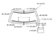
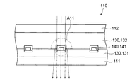
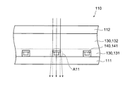
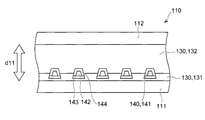
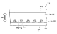
- FIG. 2 is a diagram illustrating the heat generating plates (matching plates) according to the first to third embodiments from the normal direction of the plate surfaces.
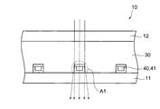
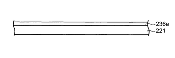
- FIG. 3 is a cross-sectional view of the heat generating plate according to the first embodiment, taken along line AA of FIG. FIG.
- FIG. 4 is a plan view showing the heating conductors of the first embodiment and the second embodiment from the normal direction of the plate surface of the heating plate, and is a plan view showing an example of the heating conductor. It is.
- FIG. 5 is a plan view showing the heat-generating conductors of the first embodiment and the second embodiment from the normal direction of the plate surface of the heat-generating plate, and shows another example of the heat-generating conductor. It is a top view.
- FIG. 6 is a diagram for explaining the operation of the heating plate of FIG.
- FIG. 7 is a diagram for explaining an example of a method of manufacturing the heating plate according to the first embodiment and the second embodiment.
- FIG. 8 is a diagram for explaining an example of a method of manufacturing the heating plate according to the first embodiment and the second embodiment.
- FIG. 9 is a diagram for explaining an example of a method of manufacturing the heating plate according to the first embodiment and the second embodiment.
- FIG. 10 is a diagram for explaining an example of a method of manufacturing the heating plate according to the first embodiment and the second embodiment.
- FIG. 11 is a diagram for explaining an example of a method of manufacturing the heating plate according to the first embodiment and the second embodiment.
- FIG. 12 is a diagram for explaining an example of a method of manufacturing the heating plate according to the first embodiment and the second embodiment.
- FIG. 13 is a diagram for explaining another example of the method of manufacturing the heat generating plates according to the first embodiment and the second embodiment.
- FIG. 14 is a diagram for explaining another example of the method for manufacturing the heating plate according to the first embodiment.
- FIG. 10 is a diagram for explaining an example of a method of manufacturing the heating plate according to the first embodiment and the second embodiment.
- FIG. 11 is a diagram for explaining an example of a method of manufacturing the heating plate according to the first embodiment and the second embodiment.
- FIG. 15 is a cross-sectional view illustrating a modification of the cross-sectional shape of the linear conductor included in the heating plate according to the first embodiment.
- FIG. 16 is a cross-sectional view showing another modification of the cross-sectional shape of the linear conductor included in the heat generating plate according to the first embodiment.
- FIG. 17 is a cross-sectional view illustrating a modified example of the linear conductor included in the heating plate according to the first embodiment.
- FIG. 18 is a diagram for explaining the operation of a conventional heat generating plate.
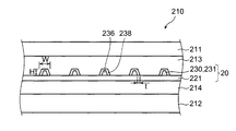
- FIG. 19 is an example of a cross-sectional view of the heat generating plate of the second embodiment taken along line AA of FIG. FIG.
- FIG. 20 is another example of a cross-sectional view of the heat generating plate according to the second embodiment taken along line AA of FIG.
- FIG. 21A is a diagram for explaining the operation of the heating plate of FIG. 19.
- FIG. 21B is a diagram for explaining the operation of the heat generating plate of FIG.
- FIG. 22 is a diagram illustrating an example of a method of manufacturing the heat generating plate according to the second embodiment.
- FIG. 23 is a diagram for explaining another example of the method of manufacturing the heat generating plate according to the second embodiment.
- FIG. 24 is a diagram for explaining another example of the method for manufacturing the heating plate according to the second embodiment.
- FIG. 25 is a cross-sectional view illustrating a modification of the cross-sectional shape of the linear conductor included in the heat generating plate according to the second embodiment.
- FIG. 26 is a cross-sectional view illustrating another modification of the cross-sectional shape of the linear conductor included in the heat generating plate according to the second embodiment.
- FIG. 27 is a cross-sectional view illustrating still another modification of the cross-sectional shape of the linear conductor included in the heat generating plate according to the second embodiment.
- FIG. 28 is a cross-sectional view illustrating still another modification of the cross-sectional shape of the linear conductor included in the heat generating plate according to the second embodiment.
- FIG. 26 is a cross-sectional view illustrating another modification of the cross-sectional shape of the linear conductor included in the heat generating plate according to the second embodiment.
- FIG. 27 is a cross-sectional view illustrating still another modification of the cross-sectional shape of the linear conductor included in the heat generating plate according to the second embodiment.
- FIG. 29 is a cross-sectional view illustrating a modification of the linear conductor included in the heat generating plate according to the second embodiment.
- FIG. 30 is a cross-sectional view illustrating another modified example of the linear conductor included in the heating plate according to the second embodiment.
- FIG. 31 is a diagram for explaining the operation of the conventional heat generating plate.
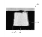
- FIG. 32 is a cross-sectional view of the laminated plate of the third embodiment taken along line AA of FIG.
- FIG. 33 is a plan view showing the patterned conductor of the third embodiment from the normal direction of the sheet surface, and is a plan view showing an example of the conductor.
- FIG. 34 is a plan view showing the patterned conductor of the third embodiment from the normal direction of the sheet surface, and is a plan view showing another example of the conductor.
- FIG. 35 is a diagram for describing an example of a method of manufacturing a plywood according to the third embodiment.
- FIG. 36 is a view for explaining an example of a method for manufacturing a plywood according to the third embodiment.
- FIG. 37 is a diagram for describing an example of a method for manufacturing a plywood according to the third embodiment.
- FIG. 38 is a diagram for describing an example of a method of manufacturing a plywood according to the third embodiment.
- FIG. 39 is a view illustrating an example of a method for manufacturing a laminated plate according to the third embodiment.
- FIG. 40 is a diagram for describing an example of a method for manufacturing a plywood according to the third embodiment.
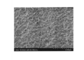
- FIG. 41 is an enlarged photograph showing a part of the linear conductor in the laminated plate according to the third embodiment.
- FIG. 42 is a photograph showing one cross section of the linear conductor in the laminated plate according to the third embodiment.
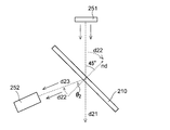
- FIG. 43 is a diagram for explaining the operation of the combination plate according to the third embodiment.
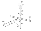
- FIG. 44 is a diagram illustrating an example of a method of measuring the luminance of light reflected by the mating plate according to the third embodiment.
- FIG. 45 is a diagram illustrating another example of a method of measuring the luminance of light reflected by the mating plate according to the third embodiment.
- FIG. 41 is an enlarged photograph showing a part of the linear conductor in the laminated plate according to the third embodiment.
- FIG. 42 is a photograph showing one cross section of the linear conductor in the laminated plate according to the third embodiment.
- FIG. 43 is a diagram for explaining the
- FIG. 46 is a graph of the example showing the relationship between the luminance measured in the state of FIG. 44 and the inclination angle of the plywood.
- FIG. 47 is a graph of a comparative example showing the relationship between the luminance measured in the state of FIG. 44 and the inclination angle of the plywood.
- FIG. 48 is an enlarged photograph showing a part of a linear conductor in an example of a conventional laminated plate.
- FIG. 49 is an enlarged photograph showing a part of a linear conductor in another example of the conventional laminated plate.
- FIG. 50 is a photograph showing one section of a linear conductor in an example of a conventional laminated plate.
- FIG. 51 is a diagram for explaining the operation of an example of a conventional laminated plate.
- the terms “plate”, “sheet”, and “film” are not distinguished from each other based only on the difference in the names.
- the “film with a conductor” is a concept including a member that can be called a plate or a sheet. Therefore, the “film with a conductor” includes a “plate with a conductor (substrate)” and a “film with a conductor”. It cannot be distinguished from a member called “sheet” only by the difference in the name.
- sheet surface refers to a target sheet-like member (plate-like member (plate-like member) when viewed as a whole and globally. Member, film-shaped member).
- FIG. 1 to FIG. 18 are diagrams for explaining the first embodiment and modifications.
- 1 is a diagram schematically showing an automobile provided with a heating plate
- FIG. 2 is a diagram of the heating plate viewed from a normal direction of the plate surface
- FIG. 3 is a diagram illustrating a cross section of the heat generating plate according to the first embodiment, taken along line -A.
- the automobile 1 as an example of the moving object has window glasses such as a front window, a rear window, and a side window.
- window glasses such as a front window, a rear window, and a side window.
- the front window 5 is constituted by the heat generating plate 10 will be described.
- the vehicle 1 has a power source 7 such as a battery.
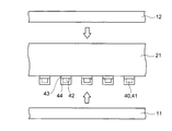
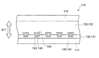
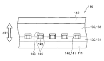
- FIG. 2 shows the heating plate 10 viewed from the normal direction of the plate surface.
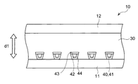
- FIG. 3 is a cross-sectional view of the heating plate 10 taken along line AA of FIG.
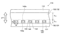
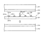
- the heating plate 10 is disposed between the first substrate 11 and the second substrate 12 that are separated from each other in the first direction d1.
- a bonding layer 30 for bonding the first substrate 11 and the second substrate 12 to each other.
- the first direction matches the thickness direction of the heating plate 10 and further matches the normal direction to the plate surface of the heating plate 10.
- the heating conductor 40 is arranged at an end of the bonding layer 30 in the first direction d1. In the examples shown in FIGS.
- FIG. 3 is a diagram showing a cross section along a direction orthogonal to a longitudinal direction of a linear conductor 41 of a heating conductor 40 described later.
- the heating plate 10 has a wiring portion 15 for supplying electricity to the heating conductor 40.
- power is supplied from the power supply 7 such as a battery to the heating conductor 40 from the wiring portion 15 through the bus bar 45 of the heating conductor 40, and the heating conductor 40 is heated by resistance heating.
- the heat generated by the heat generating conductor 40 is transmitted to the first substrate 11 and the second substrate 12, and the first substrate 11 and the second substrate 12 are warmed. Thereby, it is possible to remove the fogging due to the dew condensation attached to the first substrate 11 and the second substrate 12. If snow or ice is attached to the first substrate 11 and the second substrate 12, the snow and ice can be melted. Therefore, the occupant's field of view is well secured.
- a switch is usually inserted (connected in series) between the power supply 7 and the bus bar 45 of the heating conductor 40 in the wiring section 15. Then, only when the heating plate 10 needs to be heated, the switch is closed to energize the heating conductor 40.
- the first substrate 11 and the second substrate 12 will be described.
- a substrate having a high visible light transmittance so as not to obstruct the occupant's view.
- the material of the first substrate 11 and the second substrate 12 include soda lime glass and blue plate glass.
- the visible light transmittance of the first substrate 11 and the second substrate 12 is preferably 90% or more.
- the visible light transmittance of the first substrate 11 and the second substrate 12 is measured at a wavelength of 380 nm to 780 nm using a spectrophotometer (“UV-3100PC” manufactured by Shimadzu Corp., conforming to JIS K-0115).
- the visible light transmittance of this part may be reduced by coloring a part or the whole of the first substrate 11 and the second substrate 12. In this case, it is possible to block direct sunlight and make it difficult to visually recognize the inside of the vehicle from outside.
- the first substrate 11 and the second substrate 12 have a thickness of 1 mm or more and 5 mm or less. With such a thickness, the first substrate 11 and the second substrate 12 having excellent strength and optical characteristics can be obtained.
- the first substrate 11 and the second substrate 12 may be made of the same material and have the same configuration, or may be different from each other in at least one of the material and the configuration.
- the bonding layer 30 is disposed between the first substrate 11 and the second substrate 12, and bonds the first substrate 11 and the second substrate 12.
- layers made of various adhesive or tacky materials can be used. Further, it is preferable to use a material having a high visible light transmittance for the bonding layer 30.
- a layer made of polyvinyl butyral (PVB) can be exemplified.
- the bonding layer 30 has a first portion 31 and a second portion 32. The first portion 31 is adjacent to the heating conductor 40. The second portion 32 is located offset from the first portion 31 in the first direction d1. The first portion 31 is in contact with the first substrate 11, and the second portion 32 is in contact with the second substrate 12.
- the thickness of the bonding layer 30, that is, the length in the first direction d1, is, for example, not less than 20 ⁇ m and not more than 1000 ⁇ m. If the bonding layer 30 has a sufficient thickness, when the heat generating plate 10 is damaged, it is possible to prevent the fragments and the like of the first substrate 11 from being scattered. This is preferable because it can suppress the penetration of the heat generating plate 10.
- the thickness T1 of the first portion 31, that is, the length in the first direction d1, is shorter than the thickness T2 of the second portion, that is, the length in the first direction d1.
- the thickness T1 of the first portion 31 can be set to 20 ⁇ m or more and 100 ⁇ m or less, and can be set to 40 ⁇ m or more and 80 ⁇ m or less.
- the thickness T2 of the second portion 32 can be, for example, not less than 150 ⁇ m and not more than 1600 ⁇ m.
- the heating plate 10 is not limited to the illustrated example, and may be provided with another functional layer expected to exhibit a specific function. Further, one functional layer may exhibit two or more functions. For example, some function may be given to at least one of the first substrate 11 and the second substrate 12 of the heating plate 10 and the bonding layer 30. Examples of the functions that can be provided to the heating plate 10 include an anti-reflection (AR) function, a hard coat (HC) function having scratch resistance, an infrared shielding (reflection) function, an ultraviolet shielding (reflection) function, and an antifouling property. Functions and the like can be exemplified.
- FIGS. 4 and 5 are plan views of the heat-generating conductor 40 viewed from the normal direction of the plate surface of the heat-generating plate 10.
- FIG. 4 shows an example of an arrangement pattern of the linear conductors 41 forming the heating conductor 40
- FIG. 5 shows another arrangement pattern of the linear conductors 41 forming the heating conductor 40. An example is shown.
- the heating conductor 40 has a pair of bus bars 45 and a plurality of linear conductors 41 disposed between the pair of bus bars 45.
- the pair of bus bars 45 are arranged apart from each other in the second direction d2, and each is electrically connected to the corresponding wiring portion 15.
- the second direction d2 is a direction along the plate surface of the heat generating plate 10, and in the illustrated example, is orthogonal or substantially orthogonal to the first direction d1.
- the voltage of the power supply 7 connected to the wiring section 15 is applied between the pair of bus bars 45.
- the linear conductor 41 is connected to a pair of bus bars 45 at both ends. Therefore, the linear conductor 41 electrically connects the pair of bus bars 45.
- the linear conductor 41 When a voltage is applied through the wiring portion 15 and the bus bar 45, the linear conductor 41 generates heat by resistance heating. Then, the heat is transmitted to the first substrate 11 and the second substrate 12 via the bonding layer 30, so that the first substrate 11 and the second substrate 12 are warmed.
- the sheet resistance of the heat generating conductor 40 in accordance with the applied voltage.
- the applied voltage is about 12 V
- it is preferably 0.1 ⁇ / ⁇ or more and 1 ⁇ / ⁇ or less
- the applied voltage is about 48 V
- it is preferably 1 ⁇ / ⁇ or more and 13 ⁇ / ⁇ or less. Therefore, when the applied voltage is in the range of 12 to 48 V, the sheet resistance is preferably from 0.1 ⁇ / ⁇ to 13 ⁇ / ⁇ .
- the resistance of the heat generating conductor 40 is too large, the amount of heat generated by the heat generating conductor 40 is insufficient, and the first substrate 11 and the second substrate 12 cannot be appropriately heated. If the resistance of the heating conductor 40 is too small, the amount of heat generated in the heating conductor 40 becomes too large, and uneven heating is likely to occur between the area near the linear conductor 41 and other areas. Become.
- the heating conductors 40 can be arranged in various patterns.
- the heating conductor 40 is formed by arranging the linear conductors 41 in a mesh pattern defining a plurality of opening regions 47.
- the heating conductor 40 includes a plurality of connecting elements 48 extending between two branch points 46 and defining an open area 47. That is, the linear conductor 41 of the heating conductor 40 is configured as a group of a plurality of connection elements 48 forming the branch points 46 at both ends.
- the mesh-shaped pattern may be an irregular mesh pattern in which the shape and size of each of the opening regions 47 are not congruent and have no constant repetition period in a plane. And the size may be the same, and the opening region 47 may be a periodic lattice mesh pattern having a constant repetition period in a plane.
- the average distance between the centers of gravity of the opening regions 47 is preferably 10,000 ⁇ m or less, more preferably 7000 ⁇ m or less, and even more preferably 5000 ⁇ m or less. If the distance between the centers of gravity of the two adjacent opening regions 47 is too small, the transmittance is deteriorated and the transparency is impaired. Therefore, the average distance between the centers of gravity of the opening regions 47 is preferably 100 ⁇ m or more. .
- the heating conductor 40 includes a plurality of linear conductors 41 connecting a pair of bus bars 45 in a striped pattern. It may be formed by being arranged in. More specifically, the plurality of linear conductors 41 may be arranged with a gap 49 in a direction not parallel to the second direction d2 while extending in the second direction d2.
- the size of the gap 49 in other words, the second direction which is the arrangement direction of the gap 49.
- d2 is an average length along a non-parallel direction, in other words, an average distance between adjacent linear conductors 41 is preferably 12000 ⁇ m or less, and preferably 7000 ⁇ m or less. Is more preferable, and it is still more preferable that it is 3000 ⁇ m or less.
- the gap 49 is too small, the transmittance is deteriorated and the transparency is impaired, so that the average distance between the adjacent linear conductors 41 is preferably 100 ⁇ m or more.
- the heat generating conductor 40 is embedded in the bonding layer 30.
- the heating conductor 40 is disposed at an end of the bonding layer 30 in the first direction d1 while being embedded in the bonding layer 30. That is, the heating conductor 40 is adjacent to the bonding layer 30.
- the heating conductor 40 is in contact with the first substrate 11.
- the linear conductor 41 of the heating conductor 40 has a surface 40 a that is in contact with the first substrate 11.
- the surface roughness Sz of the surface 40a of the heat generating conductor 40 on the side in contact with the first substrate 11 is preferably 3.0 ⁇ m or less, more preferably 2.0 ⁇ m or less, and more preferably 1.0 ⁇ m or less. It is more preferred that:
- the surface roughness Sz of the surface 40b on the side adjacent to the bonding layer 30 of the heat generating conductor 40 is preferably greater than 1.0 ⁇ m, and more preferably 3.0 ⁇ m or more. Is more preferred.
- the surface roughness Sz means Sz defined by ISO25178.
- linear conductor 41 and a bus bar 45 for example, gold, silver, copper, platinum, aluminum, chromium, molybdenum, nickel, titanium, palladium, indium, tungsten, and these One or more of the alloys can be exemplified.
- the linear conductor 41 and the bus bar 45 may be formed using the same material, or may be formed using different materials.
- the linear conductor 41 can be formed using an opaque metal material as described above.
- the ratio of the region not covered by the linear conductor 41 that is, the non-coverage ratio (opening ratio) is as high as about 70% to 99%.
- the line width of the linear conductor 41 is 2 ⁇ m or more and 20 ⁇ m or less. For this reason, the region where the linear conductor 41 is provided is transparently grasped as a whole, so that the presence of the linear conductor 41 does not impair the transparency of the heating plate 10.
- the linear conductor 41 has a rectangular cross section as a whole.
- the width W of the linear conductor 41 that is, the width W along the plate surface of the heating plate 10 is 2 ⁇ m or more and 20 ⁇ m or less
- the height (thickness) H that is, the plate surface of the heating plate 10 It is preferable that the height (thickness) H along the normal line direction be 1 ⁇ m or more and 30 ⁇ m or less. According to the linear conductor 41 having such dimensions, since the linear conductor 41 is sufficiently thinned, the linear conductor 41 can be effectively made invisible.
- the ratio (H / W) of the height H to the line width W of the linear conductor 41 is preferably 0.5 or more and 1.8 or less. It is more preferably 7 or more and 1.5 or less, further preferably 0.9 or more and 1.35 or less.
- the linear conductor 41 having such a dimensional ratio is easy to manufacture, and can be configured such that the width is too large with respect to the height and does not impair the transparency. Further, even if the linear conductor 41 having such a dimensional ratio is observed from a direction inclined in the normal direction of the heating plate 10, the width of the visible linear conductor 41 hardly changes. In other words, seeing from a direction inclined in the normal direction of the heating plate 10 does not easily impair the transparency.
- the ratio (T1 / H) of the thickness T1 of the first portion 31 of the bonding layer 30 to the height H of the linear conductor 41 is preferably 3 or more and 8 or less, and more preferably 4 or more and 7 or less. Is more preferred.
- the ratio (T2 / H) of the thickness T2 of the second portion 32 of the bonding layer 30 to the height H of the linear conductor 41 is preferably 20 or more and 130 or less, and is 60 or more and 110 or less. Is more preferred. In such a case, when the heat generating conductor 40 is embedded in the first portion 31 (the base film 21) of the bonding layer 30 in the manufacturing process of the heat generating plate 10 described later, it is possible to effectively suppress the entry of air and the like. can do.
- the linear conductor 41 is formed of a conductive layer 42, a second dark layer 44 that covers the side of the surface of the conductive layer 42 that faces the first substrate 11 and both sides.
- a first dark color layer 43 that covers the surface of the conductive layer 42 on the side facing the second substrate 12 may be included.
- the linear conductor 41 includes at least a dark layer covering the surface of the second dark layer 44 on the side facing the first substrate 11.
- the conductive layer 42 made of a metal material having excellent conductivity exhibits a relatively high reflectance. When light is reflected by the conductive layer 42 forming the linear conductor 41, the reflected light becomes visible, which may obstruct the occupant's view.
- the first dark layer 43 and the second dark layer 44 cover at least a part of the surface of the conductive layer 42.
- the first dark color layer 43 and the second dark color layer 44 may be layers having a lower visible light reflectance than the conductive layer 42, and are dark layers such as black.
- the first dark color layer 43 and the second dark color layer 44 have a visible light reflectance of 15% or less, preferably 8% or less, more preferably 5% or less.
- the first dark color layer 43 and the second dark color layer 44 make it difficult for the conductive layer 42 to be visually recognized, so that the occupant's view can be secured well.
- the surface of the surface 40b of the heat generating conductor 40 adjacent to the bonding layer 30 is rough, the first dark color formed on the side surface of the conductive layer 42 formed on the surface of the linear conductor 41 The layer 43 and the second dark layer 44 are roughened.
- a heating conductor made of a tungsten wire is disposed between two substrates while being supported by a heat-sealing transparent substrate film, and is bonded. It was bonded to each substrate by layers.
- a heating wire (wire) formed of such tungsten has a relatively high volume resistivity.
- the thin heating wire is easily broken, it is also difficult to process the heating plate with high yield. For these reasons, the heating wire made of tungsten is formed thick. For this reason, the heating wire included in the heating plate is easily recognized, and the visibility of the field of view through the heating plate is deteriorated.
- a heating conductor made of a heating wire made of copper or the like and having a line width of 10 ⁇ m or less was supported on a transparent substrate made of polyethylene terephthalate (PET) or the like. In this state, it was arranged between the two bonding layers and bonded to each substrate by the bonding layers. Therefore, the heat generating conductor is hard to be visually recognized, and it is effective in obtaining good transparency.
- a voltage is applied to the heating conductor to cause the heating plate to generate heat, distortion may occur in the field of view through the heating plate. The distortion can deteriorate visibility through the heating plate.
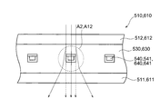
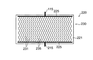
- the resin layer 530 is a layer including a bonding layer and a transparent base material.
- the refractive index of the resin layer 530 is more likely to change due to a temperature rise than the substrates 511 and 512 made of glass or the like.
- the present inventors have also confirmed that the occurrence of the difference in the refractive index in the resin layer 530 is caused by uneven temperature in the resin layer 530.
- the peripheral region A2 near each linear conductor 541 of the heating conductor 540 becomes , More susceptible to heat than other areas.
- the peripheral area A2 of the linear conductor 541 is warmed more than other areas. That is, temperature unevenness occurs between the peripheral region A2 and other regions.
- the resin layer 530 is deteriorated by heat. Due to the alteration, the refractive index of the resin layer 530 in the peripheral region A2 changes.
- a difference in the refractive index occurs between the peripheral region A2 of the resin layer 530 and the region other than the peripheral region A2.
- light transmitted between the peripheral region A2 and the region other than the peripheral region A2 is refracted as shown by a solid arrow in FIG.
- the light incident on the heat generating plate 510 passes through the heat generating plate 510 in a state where heat is generated, the light spreads far more than the dotted arrow indicating light that is not refracted and is emitted.
- the emitted light spreads more as the area A2 in which the resin layer 530 deteriorates becomes larger.
- the distortion occurs in the field of view via the heating plate 510.
- the heat generating conductor 40 has a surface 40 a in contact with the first substrate 11.
- the heat generated by the heat generating conductor 40 can be efficiently transmitted to the first substrate 11.
- the first substrate 11 made of glass or the like is more likely to conduct heat than the bonding layer 30 made of resin or the like. That is, more heat is conducted to the first substrate 11. In other words, the heat conducted to the bonding layer 30 is reduced. For this reason, the peripheral region A1 where deterioration due to heat can occur can be reduced. Since the light incident on the heating plate 10 is less likely to spread, generation of distortion can be suppressed. Further, since heat is easily transmitted to the first substrate 11, the first substrate 11 can efficiently generate heat. This is particularly effective when it is desired to efficiently generate heat only on one side of the heat generating plate 10, such as the outside of the front window 5 of the automobile 1 shown in FIG.
- the surface roughness Sz of the surface 40a of the heating conductor 40 on the side in contact with the first substrate 11 is preferably 3.0 ⁇ m or less, more preferably 2.0 ⁇ m or less, and further preferably 1.0 ⁇ m or less. It is as follows. That is, the portion where the heating conductor 40 and the first substrate 11 are in contact with each other is large. In this case, the heat generated by the heating conductor 40 can be efficiently transmitted to the first substrate 11. That is, more heat is conducted to the first substrate 11. In other words, the heat conducted to the bonding layer 30 is reduced. For this reason, the peripheral region A1 where deterioration due to heat can occur can be made smaller.
- the first substrate 11 can efficiently generate heat. This is particularly effective when only one side of the heat generating plate 10 such as the outside of the front window 5 of the automobile 1 shown in FIG.
- the surface roughness Sz of the surface 40b of the heat generating conductor 40 on the side adjacent to the bonding layer 30 is preferably larger than 1.0 ⁇ m, and more preferably 3.0 ⁇ m or more. In other words, it is preferable that a portion where the heat generating conductor 40 and the bonding layer 30 are in contact is small. In this case, the heat generated in the heating conductor 40 is not easily transmitted to the bonding layer 30 by heat conduction. For this reason, the peripheral region A1 where deterioration due to heat can occur can be made smaller. Since the light incident on the heating plate 10 is less likely to spread, the occurrence of distortion can be further suppressed.
- the heat generated in the heating conductor 40 is easily transmitted by radiation (radiation). According to the transmission of heat by radiation, local heating of the heat generating plate 10 can be avoided, and more uniform heating can be realized than the transmission by heat conduction. For this reason, the peripheral region A1 where deterioration due to heat can occur can be made smaller. Since the light incident on the heating plate 10 is less likely to spread, the occurrence of distortion can be further suppressed. Moreover, according to the transfer of heat by radiation, the first substrate 11 and the second substrate 12 can be efficiently heated, or snow, water droplets, and the like attached to the surface of the heating plate 10 can be directly heated. That is, the function of the heat generating plate 10 can be exhibited more efficiently.
- the linear conductor 41 preferably includes a first dark color layer 43 or a second dark color layer 44 provided on at least a part of the surface.
- the linear conductor 41 preferably includes the second dark layer 44 provided on the side facing the first substrate 11.
- the first substrate 11 and the second substrate 12 can be efficiently heated, or snow, water droplets, etc. attached to the surface of the heating plate 10 can be directly heated. That is, the function of the heat generating plate 10 can be exhibited more efficiently.
- the distance between the centers of gravity of two adjacent opening regions 47 is 100 ⁇ m or more and 10000 ⁇ m or less, more preferably 7000 ⁇ m or less, and further preferably 5000 ⁇ m or less.
- the average length of the gap 49 along a direction not parallel to the second direction d2 is 100 ⁇ m or more and 12000 ⁇ m or less, and more preferably 7000 ⁇ m or less. And more preferably 3,000 ⁇ m or less.
- the peripheral region A1 where deterioration due to heat can occur can be made smaller. Since the light incident on the heating plate 10 is less likely to spread, the occurrence of distortion can be further suppressed.
- the sheet resistance of the heat generating conductor 40 is 0.1 ⁇ / ⁇ or more and 1 ⁇ / ⁇ or less, more preferably 0.2 ⁇ / ⁇ or more, and further preferably 0.3 ⁇ / ⁇ or more. It has become.
- the heat generation amount is too large, so that the heat generation unevenness occurs between the area near the linear conductor 41 and other areas. This can be suppressed. For this reason, the peripheral region A1 where deterioration due to heat can occur can be made smaller. Since the light incident on the heating plate 10 is less likely to spread, the occurrence of distortion can be further suppressed.
- the ratio (T1 / H) of the thickness T1 of the first portion 31 of the bonding layer 30 to the height H of the linear conductor 41 is preferably 3 or more, and more preferably 4 or more.
- the heating conductor 40 in the manufacturing process of the heating plate 10 causes the first portion 31 of the bonding layer 30 (the base film 31).
- the heat generating conductor 40 is easily and completely embedded in the first portion 31. In other words, the heat generating conductor 40 is embedded in the first portion 31 without any gap. Therefore, entry of air or the like between the first substrate 11 and the bonding layer 30 can be effectively suppressed.
- the ratio (T2 / H) of the thickness T2 of the second portion 32 of the bonding layer 30 to the height H of the linear conductor 41 is preferably 20 or more, and more preferably 60 or more.
- the heating conductor 40 in the manufacturing process of the heating plate 10 causes the first portion 31 of the bonding layer 30 (the base film 31).
- the deformation of the first portion 31 caused by the heating conductor 40 being embedded in the first portion 31 can be easily flattened by the second portion 32. In other words, it is possible to prevent a gap from being generated between the first portion 31 and the second portion 32. Therefore, it is possible to effectively suppress air or the like from entering between the first portion 31 and the second portion 32 or between the second portion 32 and the second substrate 12.
- the ratio (T1 / H) of the thickness T1 of the first portion 31 of the bonding layer 30 to the height H of the linear conductor 41 is set so that the entire thickness of the heating plate 10 is not excessively large. , 8 or less, and more preferably 7 or less.
- the ratio (T2 / H) of the thickness T2 of the second portion 32 of the bonding layer 30 to the height H of the linear conductor 41 is preferably 130 or less, and more preferably 110 or less. More preferred.
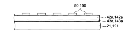
- a dark film 43a for forming the first dark layer 43 is provided on the base film 21 for forming a part of the bonding layer 30.
- the base film 21 has a heat sealing property.
- the dark color film 43a is provided in a state where it is processed to be coarse.
- the dark color film 43a is processed so as to be rough.
- the dark-colored film 43a can be treated so as to be coarse by, for example, immersing it in a mixture of an aqueous solution of sodium chlorite and an aqueous solution of sodium hydroxide. That is, the surface has a large surface roughness Sz.
- a conductive film 42a for forming the conductive layer 42 is provided on the dark film 43a.
- the conductive film 42a can be formed by a known method. For example, a method of attaching a metal foil such as a copper foil, a plating method including electroplating and electroless plating, a sputtering method, a CVD method, a PVD method, an ion plating method, or a method combining two or more of these methods is employed. can do.
- the conductive film 42a may be formed by applying a paste-like material containing a conductive metal or the like.
- two layers may be formed at the same time by sticking an electrolytic copper foil or a rolled copper foil composed of the conductive film 42a having the dark color film 43a that has been processed to be coarse.
- a resist pattern 50 is provided on the conductive film 42a.
- the resist pattern 50 has a shape corresponding to the arrangement pattern of the linear conductors 41 to be formed.
- This resist pattern 50 can be formed by patterning using a known photolithography technique.
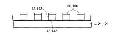
- the conductive film 42a and the dark color film 43a are etched using the resist pattern 50 as a mask. By this etching, the conductive film 42a and the dark color film 43a are patterned into a pattern substantially the same as the resist pattern 50. As a result, as shown in FIG. 9, a conductive layer 42 which forms a part of the linear conductor 41 is formed from the patterned conductive film 42a. In addition, a first dark layer 43 that forms a part of the linear conductor 41 is formed from the patterned dark film 43a.
- the etching method is not limited to wet etching using an etching solution, and a known method can be employed. As a known method, for example, plasma etching may be used. After the etching step, the resist pattern 50 is removed as shown in FIG.
- a second dark layer 44 is formed on the surface and the side of the conductive layer 42 opposite to the surface on which the first dark layer 43 is provided.
- the second dark layer 44 is formed, for example, by performing a darkening process (blackening process) on a part of the material forming the conductive layer 42, and forming a second layer made of metal oxide or metal sulfide from the part forming the conductive layer 42.
- a dark layer 44 can be formed.
- the second dark color layer 44 may be provided on the surface of the conductive layer 42.
- the surface of the conductive layer 42 may be roughened to provide the second dark layer 44.
- the conductor-attached film 20 including the heat-generating conductor 40 and the base film 21 supporting the heat-generating conductor 40 is manufactured.
- the bus bar 45 of the heating conductor 40 may be formed integrally with the conductive layer 42 of the linear conductor 41 by patterning the conductive film 42a, or may be a line provided on the base film 21.
- the conductor 41 may be separate from the conductor 41.
- the heating conductor 40 supported by the base film 21 is disposed between the first substrate 11 and the second substrate 12.
- an adhesive film 22 is disposed between the first substrate 11 and the second substrate 12 and on the side of the base film 21 of the film with conductor 20.
- the adhesive film 22 has a heat sealing property.
- the first substrate 11 and the second substrate 12 are joined by pressing and heating toward each other.
- the heating conductor 40 is embedded in the base film 21 while being in contact with the first substrate 11.
- the base film 21 and the adhesive film 22 are heated and pressed, the base film 21 becomes the first portion 31 of the bonding layer 30, and the bonding film 22 becomes the second portion 32 of the bonding layer 30.
- the bonding layer 30 is formed by the base film 21 and the adhesive film 22.
- the bonding layer 30 may be formed only from the base film 21 by making the base film 21 on which the dark film 43a and the conductive film 42a are provided with a sufficient thickness.
- the heating conductor 40 supported by the base film 21 is disposed between the first substrate 11 and the second substrate 12, and the first substrate 11 and the second substrate 12 are Press and heat toward each other to join.
- the heating conductor 40 is embedded in the base film 21 while being in contact with the first substrate 11.
- the side of the base film 21 on which the heating conductor 40 is provided is from the side opposite to the side of the base film 21 on which the heating conductor 40 is provided to support the heating conductor 40. , So that the hardness is high.
- the side of the heat generating conductor 40 of the base film 21 having the higher hardness becomes the first portion 31 of the bonding layer 30 and is separated from the heat generating conductor 40 of the base film 21 having the lower hardness.
- the side becomes the second portion 32 of the bonding layer 30.
- the heating plate 10 shown in FIG. 3 is also manufactured in such a process.
- the heat generating plate 10 is provided between the first substrate 11 and the second substrate 12 that are spaced apart from each other in the first direction d1.
- the heat generating conductor 40 includes a heating conductor 40 that is disposed and generates heat when a voltage is applied thereto, and a bonding layer 30 that bonds the first substrate 11 and the second substrate 12 together.
- the heating conductor 40 has a surface in contact with the first substrate 11. According to such a heating plate 10, heat generated by the heating conductor 40 can be efficiently transmitted to the first substrate 11. In other words, the heat conducted to the bonding layer 30 is reduced. For this reason, the peripheral region A1 where deterioration due to heat can occur can be reduced. Therefore, it is possible to suppress the occurrence of distortion in the field of view via the heating plate 10 while the heating plate 10 is generating heat.
- the surface roughness Sz of the heat generating conductor 40 on the side in contact with the first substrate 11 is 3.0 ⁇ m or less. According to such a heating plate 10, heat generated by the heating conductor 40 can be efficiently transmitted to the first substrate 11. For this reason, more heat is conducted to the first substrate 11, and the peripheral region A1 where deterioration due to heat may occur can be made smaller. Therefore, since the light incident on the heat generating plate 10 is hardly spread, the occurrence of distortion can be further suppressed.
- the method of manufacturing the heat generating plate 10 according to the first embodiment includes a step of providing the conductive film 42a on the base film 21 having heat sealing properties, a step of patterning the conductive film 42a, and a step of forming the first substrate 11 and A step of pressing and heating the first substrate 11 and the second substrate 12 toward each other in a state where the base film 21 is disposed between the second substrates 12 and joining them.
- the method for manufacturing the heating plate 10 since the conductive film 42 a that forms the conductive layer 42 is formed on the base film 21 having heat sealing properties, the above-described heating plate 10 can be easily manufactured. Can be.
- the heat generating plate 10 is formed in a curved shape.
- the present invention is not limited to this example, and the heat generating plate 10 may be formed in a flat shape.
- the linear conductor 41 has a rectangular cross section. That is, in the cross section of the linear conductor 41, opposing sides in the first direction d1 are parallel and have the same length.
- the linear conductor 41 is not limited to a rectangular shape, and may have, for example, a trapezoidal cross section. Further, the linear conductor 41 may have different lengths on opposite sides facing the first direction d1.
- the cross-sectional shape of the linear conductor 41 may be a trapezoidal shape in which the side in contact with the first substrate 11 is the shorter side of the two opposite sides parallel to each other.
- the linear conductor 41 may have different widths on opposite sides in a cross section along the first direction d1.
- the width of the linear conductor 41 in a direction orthogonal to the first direction d1 may be narrower at a position closest to the second substrate 12 than at a position in contact with the first substrate 11.
- the width of the linear conductor 41 along a direction orthogonal to the first direction d1 may be gradually reduced from the first substrate 11 side to the second substrate 12 side.
- the legs in the cross section of the linear conductor 41 that is, the side surfaces of the linear conductor 41 may be inclined toward a direction orthogonal to the first direction and face the second substrate 12. it can. For this reason, the heat transmitted by the radiation from the side surface of the linear conductor 41 tends to travel to the second substrate 12. That is, not only the first substrate 11 but also the second substrate 12 can be appropriately heated.
- the side surface of the linear conductor 41 is not limited to a straight line as in the example shown in FIG. 15 in a cross section along the first direction d1, but may be curved.
- the surface roughness Sz of the side surface of the linear conductor 41 is larger than 1.0 ⁇ m, local heating of the heating plate 10 is avoided by radiation from the side surface of the linear conductor 41 to make the heating plate 10 uniform.
- the heat can be transferred to the second substrate 12 while being heated.
- the second substrate 12 can efficiently generate heat.
- the side surface of the linear conductor 41 includes the second dark layer 44, radiation from the side surface of the linear conductor 41 can be promoted. It is possible to efficiently transfer heat to the second substrate 12 while uniformly heating the heating plate 10 by effectively avoiding local heating of the heating plate 10 by radiation from the side surface of the linear conductor 41. it can. In other words, the second substrate 12 can generate heat more efficiently.
- the heating conductor 40 supported by the base film 21 in a state where the heating conductor 40 supported by the base film 21 is disposed between the first substrate 11 and the second substrate 12, the first substrate 11 and the second In the step of pressing and heating the two substrates 12 toward each other and joining them, the legs in the cross section of the linear conductor 41, that is, the side surfaces of the linear conductor 41 are inclined with respect to a direction orthogonal to the first direction d1.
- the heating conductor 40 is embedded in the base film 21 when facing the side of the second substrate 12, air flows between the first substrate 11 and the base film 21 and the heating conductor 40. And the like can be effectively suppressed. Therefore, it is possible to prevent the visibility through the heating plate 10 from being deteriorated by the bubbles.
- the cross-sectional shape of the linear conductor 41 may be a trapezoidal shape in which the side in contact with the first substrate 11 is the longer side of the two opposite sides that are parallel.
- the width of the linear conductor 41 in a direction orthogonal to the first direction d1 may be wider at a position closest to the second substrate 12 than at a position in contact with the first substrate 11.
- the width of the linear conductor 41 along a direction orthogonal to the first direction d1 may be gradually increased from the first substrate 11 side to the second substrate 12 side.
- the legs in the cross section of the linear conductor 41 that is, the side surfaces of the linear conductor 41 may be inclined with respect to a direction orthogonal to the first direction d1 and face the first substrate 11 side. it can. For this reason, the heat transmitted by the radiation from the side surface of the linear conductor 41 tends to travel to the first substrate 11. That is, the first substrate 11 can be efficiently heated.
- the side surface of the linear conductor 41 is not limited to a straight line as in the example shown in FIG. 15 in a cross section along the first direction d1, but may be curved.
- the surface roughness Sz of the side surface of the linear conductor 41 is greater than 1.0 ⁇ m, local heating of the heating plate 10 is avoided by radiation from the side surface of the linear conductor 41 to make the heating plate 10 uniform.
- the heat can be efficiently transmitted to the first substrate 11 while being heated.
- the entire first substrate 11 can be efficiently heated.
- the side surface of the linear conductor 41 includes the second dark layer 44, radiation from the side surface of the linear conductor 41 can be promoted. Radiation from the side surface of the linear conductor 41 effectively avoids local heating of the heating plate 10 and efficiently transfers heat to the first substrate 11 while uniformly heating the heating plate 10. it can. In other words, the entire first substrate 11 can be more efficiently heated.
- the linear conductor 41 having such a tapered cross-sectional shape is formed by, for example, making the dark-colored film 43a forming the first dark-colored layer 43 more difficult to be etched than the conductive film 42a forming the conductive layer 42.
- it can be formed by being easily etched. That is, if the dark color film 43a is less likely to be etched than the conductive film 42a, the dissolution of the dark color film 43a is less likely to progress than the conductive film 42a, and the etching of the conductive film 42a on the side of the dark color film 43a is less likely to progress. Therefore, as shown in FIG.
- the cross-sectional shape of the linear conductor 41 is tapered toward the side in contact with the first substrate 11, typically, the cross-sectional shape of the linear conductor 41 is the first shape.
- the side in contact with the substrate 11 has a trapezoidal shape that is the shorter side of the two opposite sides that are parallel (substantially parallel). If the dark film 43a is more easily etched than the conductive film 42a, the dissolution of the dark film 43a proceeds from the conductive film 42a, and the conductive film 42a is also etched from the side of the dissolved dark film 43a. Therefore, as shown in FIG.
- the cross-sectional shape of the linear conductor 41 has a tapered shape tapered toward the side in contact with the first substrate 11, and typically, the side in contact with the first substrate 11 is parallel ( It has a trapezoidal shape that is the shorter side of the two opposite sides (substantially parallel).
- the second dark layer 44 may be provided as follows. First, after the conductive film 42a and the dark color film 43a are patterned into substantially the same pattern as the resist pattern 50 by an etching process, the second dark color layer roughened on the side surface of the conductive layer 42 without removing the resist pattern 50. 44 is formed. Thereafter, the resist pattern 50 is removed, and another part of the second dark color layer 44 that is not roughened is formed on the surface of the conductive layer 42 opposite to the surface on which the first dark color layer 43 is provided.
- the surface roughness Sz of the heating conductor 40 on the side in contact with the first substrate 11 can be easily reduced. That is, the surface roughness Sz of the heat generating conductor 40 on the side in contact with the first substrate 11 can be easily reduced to 3.0 ⁇ m or less.
- the second dark layer 44 may not be provided on the side in contact with the first substrate 11. That is, the second dark layer 44 may be provided only on the side surface of the conductive layer 42.
- Such a second dark layer 44 is formed on the side surface of the conductive layer 42 without removing the resist pattern 50 after the conductive film 42a and the dark film 43a are patterned into substantially the same pattern as the resist pattern 50 by an etching process. It can be provided by forming a part of the roughened second dark layer 44.
- the conductive layer 42 is exposed on the side in contact with the first substrate 11.
- the conductive layer 42 has a small surface roughness. Therefore, the surface roughness Sz of the heat generating conductor 40 on the side in contact with the first substrate 11 can be easily reduced. That is, the surface roughness Sz of the heat generating conductor 40 on the side in contact with the first substrate 11 can be easily reduced to 3.0 ⁇ m or less.
- FIGS. 1, 2, 4, 5, 7 to 13, and 18 to 31 are diagrams for explaining the second embodiment and modifications.
- 1 is a diagram schematically showing an automobile provided with a heating plate
- FIG. 2 is a diagram of the heating plate viewed from a normal direction of the plate surface
- FIGS. 19 and 20 are diagrams of FIG. It is a figure showing an example of a section of a heat generating plate concerning a 2nd embodiment along another AA line of Drawing 2, and another example.
- the automobile 101 as an example of the moving object has window glasses such as a front window, a rear window, and a side window.
- window glasses such as a front window, a rear window, and a side window.
- the front window 105 is constituted by the heat generating plate 110 is illustrated.
- the automobile 101 has a power supply 107 such as a battery.
- FIG. 2 shows the heating plate 110 viewed from the normal direction of the plate surface.
- FIGS. 19 and 20 are cross-sectional views of the heat generating plate 110 shown in FIG. 2 taken along the line AA.
- the heating plate 110 is formed by the first substrate 111 and the second substrate 112 that are separated from each other in the first direction d11 and the first substrate 111 and the second substrate 112. It has a heat-generating conductor 140 disposed therebetween and a bonding layer 130 for bonding the first substrate 111 and the second substrate 112.
- the first direction d11 matches the thickness direction of the heating plate 110, and further matches the normal direction to the plate surface of the heating plate 110.
- FIG. 19 and 20 are cross-sectional views of the heat generating plate 110 shown in FIG. 2 taken along the line AA.
- the heating plate 110 is formed by the first substrate 111 and the second substrate 112 that are separated from each other in the first direction d11 and the first substrate 111 and the second substrate 112. It has a heat-generating conductor 140
- the heat generating conductor 140 is disposed at an intermediate portion of the bonding layer 130 in the first direction d11.
- the heat generating conductor 140 is disposed at an end of the bonding layer 130 in the first direction d11.
- the heating plate 110 is curved, but in other drawings, the heating plate 110, the first substrate 111, The second substrate 112 is illustrated as a flat plate.
- FIGS. 19 and 20 are views showing a cross section along a direction orthogonal to the longitudinal direction of the linear conductor 141 of the heat generating conductor 140 described later.
- the heating plate 110 has a wiring portion 115 for supplying electricity to the heating conductor 140.
- the power supply 107 such as a battery supplies electricity to the heating conductor 140 from the wiring section 115 via the bus bar 145 of the heating conductor 140, and causes the heating conductor 140 to generate heat by resistance heating.
- the heat generated by the heat generating conductor 140 is transmitted to the first substrate 111 and the second substrate 112, and the first substrate 111 and the second substrate 112 are heated. Accordingly, it is possible to remove the fogging due to the dew attached to the first substrate 111 and the second substrate 112. When snow or ice is attached to the first substrate 111 and the second substrate 112, the snow or ice can be melted.
- a switch is usually inserted (connected in series) between the power supply 107 and the bus bar 145 of the heating conductor 140 in the wiring section 115. Then, only when the heating plate 110 needs to be heated, the switch is closed to energize the heating conductor 140.
- the first substrate 111 and the second substrate 112 will be described.
- the first substrate 111 and the second substrate 112 are used for a front window of an automobile as in the example shown in FIG.
- the first substrate 111 and the second substrate 112 preferably have a visible light transmittance of 90% or more.
- the material of the first substrate 111 and the second substrate 112 include soda lime glass and blue plate glass.
- the visible light transmittance of a part of the first substrate 111 and the second substrate 112 may be reduced by coloring a part or the whole of the first substrate 111 and the second substrate 112. In this case, it is possible to block direct sunlight and make it difficult to visually recognize the inside of the vehicle from outside.
- the first substrate 111 and the second substrate 112 have a thickness of 1 mm or more and 5 mm or less. With such a thickness, the first substrate 111 and the second substrate 112 having excellent strength and optical characteristics can be obtained.
- the first substrate 111 and the second substrate 112 may be made of the same material and have the same structure, or may be different from each other in at least one of the material and the structure.
- the bonding layer 130 is disposed between the first substrate 111 and the second substrate 112, and bonds the first substrate 111 and the second substrate 112.
- a layer made of various adhesive or tacky materials can be used. Further, it is preferable to use a material having a high visible light transmittance for the bonding layer 130.
- a layer made of polyvinyl butyral (PVB) can be exemplified. 19 and 20, the bonding layer 130 has a first portion 131 and a second portion 132. The first portion 131 is adjacent to the heating conductor 140. The first portion 131 and the second portion 132 have different properties and are shifted from each other in the first direction d11.
- the first portion 131 satisfies at least one of the following: a smaller amount of the plasticizer per unit mass included, a higher glass transition temperature, and a higher softening point than the second portion 132. ing.
- the amount of the plasticizer per unit mass, the glass transition temperature, and the softening point of the first portion 131 and the second portion 132 are determined by, for example, the content of the additive added to the first portion 131 and the amount added to the second portion 132. It can be set appropriately by adjusting the content of the additive to be added.
- the amount of the plasticizer contained in the first portion 131 can be set to 25 wt% or less, the glass transition temperature can be set to 60 ° C or higher, and the softening point can be set to 110 ° C or higher.
- the amount of the plasticizer contained can be 15 wt% or less, the glass transition temperature can be 65 ° C or more, and the softening point can be 140 ° C or more.
- the unit [wt%] represents the mass percent concentration.
- the thickness T1 of the first portion 131 is shorter than the thickness T2 of the second portion 132, that is, the length in the first direction d11.
- the thickness T1 of the first portion 131 can be set to 20 ⁇ m or more and 100 ⁇ m or less, and further, 40 ⁇ m or more and 80 ⁇ m or less.
- the thickness T2 of the second portion 132 can be selected according to the safety performance of the laminated glass, and a certain thickness is required to enhance the penetration performance of an impact object when the glass is broken and the scattering of glass fragments. However, it can be set to, for example, 150 ⁇ m or more and 1600 ⁇ m or less.
- the heating plate 110 is not limited to the illustrated example, and may be provided with another functional layer expected to exhibit a specific function. Further, one functional layer may exhibit two or more functions. For example, some function may be given to at least one of the first substrate 111 and the second substrate 112 of the heating plate 110 and the first portion 131 and the second portion 132 of the bonding layer 130.
- the functions that can be provided to the heat generating plate 110 include an anti-reflection (AR) function, a hard coat (HC) function having scratch resistance, an infrared shielding (reflection) function, an ultraviolet shielding (reflection) function, and an antifouling property. Functions and the like can be exemplified.
- FIGS. 4 and 5 are plan views of the heat generating conductor 140 as viewed from the normal direction of the plate surface of the heat generating plate 110.
- FIG. FIG. 4 shows an example of an arrangement pattern of the linear conductors 141 forming the heating conductor 140
- FIG. 5 shows another arrangement pattern of the linear conductors 141 forming the heating conductor 140. An example is shown.
- the heat generating conductor 140 has a pair of bus bars 145 and a plurality of linear conductors 141 disposed between the pair of bus bars 145.
- the pair of bus bars 145 are arranged apart from each other in the second direction d12, and each is electrically connected to the corresponding wiring portion 115.
- the second direction d12 is a direction along the plate surface of the heat generating plate 110, and in the illustrated example, is orthogonal or substantially orthogonal to the first direction d11.
- the voltage of the power supply 107 connected to the wiring section 115 is applied between the pair of bus bars 145.
- the linear conductor 141 is connected to a pair of bus bars 145 at both ends. Therefore, the linear conductor 141 electrically connects the pair of bus bars 145.
- the linear conductor 141 When a voltage is applied to the linear conductor 141 via the wiring portion 115 and the bus bar 145, the linear conductor 141 generates heat by resistance heating. Then, the heat is transmitted to the first substrate 111 and the second substrate 112 via the bonding layer 130, so that the first substrate 111 and the second substrate 112 are heated.
- the sheet resistance of the heat generating conductor 140 in accordance with the applied voltage.
- the applied voltage is about 12 V
- it is preferably 0.1 ⁇ / ⁇ or more and 1 ⁇ / ⁇ or less
- the applied voltage is about 48 V
- it is preferably 1 ⁇ / ⁇ or more and 13 ⁇ / ⁇ or less. Therefore, when the applied voltage is in the range of 12 to 48 V, the sheet resistance is preferably from 0.1 ⁇ / ⁇ to 13 ⁇ / ⁇ .
- the resistance of the heating conductor 140 is too large, the amount of heat generated by the heating conductor 140 is insufficient, and the first substrate 111 and the second substrate 112 cannot be appropriately heated. On the other hand, if the resistance of the heating conductor 140 is too small, the amount of heat generated in the heating conductor 140 becomes too large, and uneven heating is likely to occur between a region near the linear conductor 141 and another region. Become.
- the heat generating conductor 140 can be arranged in various patterns.
- the heating conductor 140 is formed by arranging the linear conductors 141 in a mesh pattern defining a plurality of opening regions 147. ing.
- the heating conductor 140 includes a plurality of connection elements 148 extending between two branch points 146 and defining an open area 147. That is, the linear conductor 141 of the heating conductor 140 is configured as a group of a plurality of connection elements 148 forming the branch points 146 at both ends. As shown in FIG.
- the mesh pattern may be an irregular mesh pattern in which the shape and size of each opening region 147 are not congruent and have no fixed repetition period in a plane, or may be a shape of each opening region 147. And the size may be congruent, and the opening region 147 may be a periodic lattice mesh pattern having a constant repetition period within a plane.
- the average distance between the centers of gravity of the opening regions 147 Is preferably 10,000 ⁇ m or less, more preferably 7000 ⁇ m or less, and even more preferably 5000 ⁇ m or less. Further, if the distance between the centers of gravity of the two adjacent opening regions 147 is too small, the transmittance is deteriorated and the transparency is impaired, so that the average distance between the centers of gravity of the opening regions 147 is preferably 100 ⁇ m or more. .
- the heating conductor 140 includes a plurality of linear conductors 141 that connect a pair of bus bars 145 arranged in a stripe pattern. It is formed by doing. More specifically, the plurality of linear conductors 141 are arranged with a gap 149 in a direction not parallel to the second direction d12 while extending in the second direction d12.
- an average distance between adjacent linear conductors 141 is preferably 12000 ⁇ m or less, and is preferably 7000 ⁇ m or less. Is more preferable, and it is still more preferable that it is 3000 ⁇ m or less. If the gap 149 is too small, the transmittance is deteriorated and the transparency is impaired. Therefore, the average of the distance between the adjacent linear conductors 141 is preferably 100 ⁇ m or more.
- the heat generating conductor 140 is embedded in the bonding layer 130.
- the heating conductor 140 is disposed between the first portion 131 and the second portion 132 of the bonding layer 130.
- the heat generating conductor 140 is disposed at an intermediate portion of the bonding layer 130 in the first direction d11.
- the heating conductor 140 is adjacent to the second portion 132 as well as the first portion 131.
- the first portion 131 of the bonding layer 130 is in contact with the first substrate 111
- the second portion 132 is in contact with the second substrate 112.
- FIG. 19 the heat generating conductor 140 is embedded in the bonding layer 130.
- the heating conductor 140 is disposed between the first portion 131 and the second portion 132 of the bonding layer 130.
- the heat generating conductor 140 is disposed at an intermediate portion of the bonding layer 130 in the first direction d11.
- the heating conductor 140 is adjacent to the second portion 132 as well as the first portion 131.
- the first portion 131 of the bonding layer 130 is in
- the heat generating conductor 140 is disposed at an end of the bonding layer 130 in the first direction d11 while being embedded in the bonding layer 130. That is, the heating conductor 140 is adjacent to the bonding layer 130. The heat generating conductor 140 is in contact with the first substrate 111. Further, in the cross section illustrated in FIG. 20, the linear conductor 141 of the heating conductor 140 has a surface 140 a that is in contact with the first substrate 111.
- the surface roughness Sz of the surface 140a of the heating conductor 140 on the side in contact with the first substrate 111 is preferably 3.0 ⁇ m or less, more preferably 2.0 ⁇ m or less, and more preferably 1.0 ⁇ m or less. It is more preferred that:
- the surface roughness Sz of the surface 140b of the heating conductor 140 on the side adjacent to the bonding layer 130 is preferably larger than 1.0 ⁇ m, and more preferably 3 ⁇ m or more. More preferably, it is.
- Examples of a material for forming the linear conductor 141 and the bus bar 145 include gold, silver, copper, platinum, aluminum, chromium, molybdenum, nickel, titanium, palladium, indium, tungsten, and these. One or more of the alloys can be exemplified.
- the linear conductor 141 and the bus bar 145 may be formed using the same material, or may be formed using different materials.
- the linear conductor 141 can be formed using an opaque metal material as described above.
- the ratio of the region not covered by the linear conductor 141 that is, the non-coverage ratio (opening ratio) is as high as about 70% to 99%.
- the line width of the linear conductor 141 is 2 ⁇ m or more and 20 ⁇ m or less. For this reason, the region where the linear conductor 141 is provided is transparently grasped as a whole, so that the presence of the linear conductor 141 does not impair the transparency of the heating plate 110.
- the linear conductor 141 has a rectangular cross section as a whole.
- the width W of the linear conductor 141 that is, the width W along the plate surface of the heating plate 110 is 2 ⁇ m or more and 20 ⁇ m or less
- the height (thickness) H that is, the plate surface of the heating plate 110 It is preferable that the height (thickness) H along the normal direction to be not less than 1 ⁇ m and not more than 30 ⁇ m. According to the linear conductor 141 having such dimensions, since the linear conductor 141 is sufficiently thinned, the linear conductor 141 can be effectively made invisible.
- the ratio (H / W) of the height H to the line width W of the linear conductor 141 is preferably 0.5 or more and 1.8 or less. It is more preferably 7 or more and 1.5 or less, further preferably 0.9 or more and 1.35 or less.
- the linear conductor 141 having such a dimensional ratio is easy to manufacture, and can prevent the visibility from being impaired due to the width being too large relative to the height. Further, even when the linear conductor 141 having such a dimensional ratio is observed from a direction inclined in the normal direction of the heating plate 110, the width of the visible linear conductor 141 hardly changes. In other words, seeing from a direction inclined in the normal direction of the heating plate 110 does not easily impair the transparency.
- the ratio (T1 / H) of the thickness T1 of the first portion 131 of the bonding layer 130 to the height H of the linear conductor 141 is 3 or more and 8 or less. , And more preferably 4 or more and 7 or less. Further, the ratio (T2 / H) of the thickness T2 of the second portion 132 of the bonding layer 130 to the height H of the linear conductor 141 is preferably 20 or more and 130 or less, and is 60 or more and 110 or less. Is more preferred.
- the linear conductor 141 is formed of the conductive layer 142 and the first dark layer 143 which covers the surface of the conductive layer 142 on the side facing the first substrate 111.
- the second dark color layer 144 may cover the surface of the conductive layer 142 facing the second substrate 112 and the both sides.
- the linear conductor 141 preferably includes at least the first dark layer 143.
- the conductive layer 142 made of a metal material having excellent conductivity exhibits a relatively high reflectance. When light is reflected by the conductive layer 142 forming the linear conductor 141, the reflected light becomes visible, which may obstruct the occupant's view.
- the first dark layer 143 and the second dark layer 144 cover at least a part of the surface of the conductive layer 142.
- the first dark layer 143 and the second dark layer 144 may be layers having a lower visible light reflectance than the conductive layer 142, and are dark layers such as black.
- the first dark color layer 143 and the second dark color layer 144 have a visible light reflectance of 15% or less, preferably 8% or less, more preferably 5% or less.
- the first dark color layer 143 and the second dark color layer 144 make it difficult for the conductive layer 142 to be visually recognized, so that the occupant's view can be secured well.
- the first dark color formed on the side surface of the conductive layer 142 formed on the surface of the linear conductor 141 is roughened.
- a heating conductor made of a tungsten wire is disposed between two substrates while being supported by a heat-sealing transparent substrate film, and is bonded. It was bonded to each substrate by layers.
- a heating wire (wire) formed of such tungsten has a relatively high volume resistivity.
- the thin heating wire is easily broken, it is also difficult to process the heating plate with high yield. For these reasons, the heating wire made of tungsten is formed thick. For this reason, the heating wire included in the heating plate is easily recognized, and the visibility of the field of view through the heating plate is deteriorated.
- a heating conductor made of a heating wire made of copper or the like and having a line width of 10 ⁇ m or less was supported on a transparent substrate made of polyethylene terephthalate (PET) or the like. In this state, it was arranged between the two bonding layers and bonded to each substrate by the bonding layers. Therefore, the heat generating conductor is hard to be visually recognized, and it is effective in obtaining good transparency.
- a voltage is applied to the heating conductor to cause the heating plate to generate heat, distortion may occur in the field of view through the heating plate. The distortion can deteriorate visibility through the heating plate.
- the resin layer 630 is a layer including a bonding layer.
- the refractive index of the resin layer 630 is more likely to change due to a temperature rise than the substrates 611 and 612 made of glass or the like.
- the present inventors have also confirmed that the occurrence of the difference in the refractive index in the resin layer 630 is caused by uneven temperature in the resin layer 630.
- the peripheral region A12 near each linear conductor 641 of the heating conductor 640 has a higher heat than other regions. Easy to receive. In other words, the peripheral area A12 of the linear conductor 641 is warmed more than other areas. That is, temperature unevenness occurs between the peripheral area A12 and other areas.
- the resin layer 630 is deteriorated by heat. Due to the alteration, the refractive index of the resin layer 630 in the peripheral area A12 changes. Thus, a difference in refractive index occurs between the peripheral region A12 of the resin layer 630 and the region other than the peripheral region A12.
- the light transmitted between the peripheral area A12 and the area other than the peripheral area A12 is refracted as shown by a solid arrow in FIG.
- the light path is largely changed compared with the dotted arrow indicating light that is not refracted, and then emitted.
- the emitted light spreads more as the area A12 where the quality of the resin layer 630 deteriorates becomes larger.
- the distortion occurs in the field of view via the heating plate 610.
- the heating plate 610 when the heating plate 610 includes the transparent substrate 635 that supports the heating conductor 640, a difference in the refractive index occurs between the bonding layers 631, 632 and the transparent substrate 635. For this reason, as shown by the solid line arrows in FIG. 31, the light transmitted through the bonding layers 631 and 632 is out of the peripheral area A13 near the linear conductor 641 and the peripheral area A13 near the linear conductor 641 that is altered by the heat generation of the heat generation conductor 640. Are refracted at the interface between the transparent substrate 635 and the interface between the bonding layers 631 and 632 and the transparent substrate 635.
- the light incident on the heat generating plate 610 changes its course largely and is emitted as compared with the dotted arrow indicating light that is not refracted.
- the emitted light is greatly spread due to a change in the course. Distortion occurs in the field of view through the heat generating plate 610 because the path of light emitted through the heat generating plate 610 is largely changed and emitted.
- the transparent base material 635 has higher rigidity and is less likely to shrink than the bonding layers 631 and 632, wrinkles and variations in thickness are likely to occur in the transparent base material 635 when the heating plate 610 is processed.
- a step may be generated in the heating conductor 640.
- the interface where the refractive index difference occurs between the bonding layers 631 and 632 and the transparent substrate 635 may be a curved surface having a locally large curvature as shown in FIG. Therefore, light transmitted through the bonding layers 631 and 632 is refracted by a curved surface having a large curvature.
- the light incident on the heating plate 610 changes its course more than the dotted arrow indicating the light that is not refracted and exits, and a greater distortion may occur in the field of view via the heating plate 610.
- strain may also occur in a region other than the peripheral region A13 near the linear conductor 641 which is degraded by the heat generation of the heating conductor 640.
- light incident on the heat generating plate 610 including the transparent base material 635 causes a difference in refractive index between the bonding layers 631 and 632 and the transparent base material 635 to cause a difference between the bonding layers 631 and 632 and the transparent base material 635. Reflection and scattering can occur at the interface. Further, due to the retardation of the transparent base material 635, rainbow unevenness may occur in the field of view via the heating plate 610. These may deteriorate the field of view through the heating plate 610.
- the heat-generating conductor 640 is fixed on the transparent base material 635.
- An adhesive may be provided.
- the adhesive in the heating plate 610, not only between the bonding layers 631 and 632 and the transparent substrate 635, but also between the bonding layer 631 and the adhesive and between the adhesive and the transparent substrate 635. causes a refractive index difference. Therefore, the light incident on the heating plate 610 is refracted at the interface between the bonding layer 631 and the adhesive and at the interface between the adhesive and the transparent substrate 635. That is, the light incident on the heating plate 610 changes its course largely and exits, and distortion occurs in the field of view via the heating plate 610.
- air may be mixed between the transparent base material 635 and the bonding layers 631 and 632 in the manufacturing process of the heating plate 610. Oxygen contained in the entrained air can oxidize the transparent substrate 635 and the adhesive. Since the transparent base material 635 and the adhesive turn yellow when oxidized, visibility through the heating plate 610 may be deteriorated.
- the first portion 131 of the bonding layer 130 has a unit weight At least one of the following: a small amount of the plasticizer, a high glass transition temperature, and a high softening point.
- the first portion 131 is less likely to be deteriorated by heat than the second portion 132.
- the first portion 131 is adjacent to the heat generating conductor 140.
- the peripheral area A11 see FIGS. 21A and 21B
- the linear conductor 141 of the heat generating conductor 40 in which deterioration due to heat may occur is compared with the peripheral area A12 in the conventional heating plate 610 where deterioration may occur. , Can be smaller.
- the light incident on the heating plate 110 passes through the heating plate 110 in a state where heat is generated, and is slightly smaller than the dotted arrow indicating light that is not refracted.
- the light exits without changing the course. In this way, the occurrence of distortion can be suppressed as compared with the conventional heating plate 610.
- FIG. 21A shows the operation of the heating plate 110 shown in FIG. 19, and FIG. 21B shows the operation of the heating plate 110 shown in FIG.
- the first portion 131 satisfies at least one of a plasticizer amount of 25 wt% or less, a glass transition temperature of 60 ° C. or more, and a softening point of 110 ° C. or more.
- the size of the peripheral region A11 where the deterioration may occur can be effectively reduced by the heat that can be transmitted to the first portion 131. Therefore, the generation of distortion can be effectively suppressed in the field of view via the heating plate 110.
- the first portion 131 must satisfy at least one of the following: the amount of the plasticizer is 15 wt% or less, the glass transition temperature is 65 ° C or more, and the softening point is 140 ° C or more. More preferably, the amount of the plasticizer satisfies at least one of 0 wt%, a glass transition temperature of 70 ° C. or higher, and a softening point of 175 ° C. or higher.
- the thickness T1 of the first portion 131 is smaller than the thickness T2 of the second portion 132.
- the thickness T1 of the first portion 131 is not less than 20 ⁇ m and not more than 100 ⁇ m, and more preferably not more than 80 ⁇ m. Since the thickness T1 of the first portion 131, which is less likely to be altered by heat, is smaller, the entire joining layer 130 can be more easily caused to be altered by heat. Therefore, bonding of the first substrate 111 and the second substrate 112 by the bonding layer 130 can be easily performed.
- the heating conductor 140 is arranged between the first portion 131 and the second portion 132 of the bonding layer 130 and is adjacent to the second portion 132. That is, the heat generating conductor 140 is disposed at an intermediate portion of the bonding layer 130 in the first direction d11, and is adjacent to both the first portion 131 and the second portion 132. Therefore, the heat generating plate 110 can stably hold the heat generating conductor 140. Further, when the first portion 131 is thinner than the second portion 132, it is possible to easily transfer heat generated by the heat generating conductor 140 to the first substrate 111 via the first portion 131. That is, more heat is conducted to the first substrate 111. In other words, the heat conducted to the bonding layer 130 is reduced.
- the peripheral area A11 where deterioration due to heat can occur can be made smaller. Since the path of the light incident on the heating plate 110 changes only slightly, the occurrence of distortion can be further suppressed. Further, since heat is easily transmitted to the first substrate 111, the first substrate 111 can efficiently generate heat. This is particularly effective when it is desired to efficiently generate heat on only one side of the heat generating plate 110, such as the outside of the front window 105 of the automobile 101 shown in FIG.
- the heat generating conductor 140 has a surface 140 a that is in contact with the first substrate 111.
- heat generated by the heat generating conductor 140 can be efficiently transmitted to the first substrate 111.
- the first substrate 111 made of glass or the like is more likely to conduct heat than the bonding layer 130 made of resin or the like. That is, more heat is conducted to the first substrate 111. In other words, the heat conducted to the bonding layer 130 is reduced. For this reason, the peripheral region A11 where deterioration due to heat can occur can be reduced.
- the path of the light incident on the heating plate 110 changes only slightly, the occurrence of distortion can be suppressed. Further, since heat is easily transmitted to the first substrate 111, the first substrate 111 can efficiently generate heat. This is particularly effective when it is desired to efficiently generate heat on only one side of the heat generating plate 110, such as the outside of the front window 105 of the automobile 101 shown in FIG.
- the linear conductor 141 preferably has a surface 140 a in contact with the first substrate 111.
- heat generated by the heat generating conductor 140 can be efficiently transmitted to the first substrate 111. That is, more heat is conducted to the first substrate 111. In other words, the heat conducted to the bonding layer 130 is reduced. For this reason, the peripheral area A11 where deterioration due to heat can occur can be made smaller. Since the path of the light incident on the heating plate 110 changes only slightly, the occurrence of distortion can be further suppressed. Further, since heat is easily transmitted to the first substrate 111, the first substrate 111 can efficiently generate heat. This is particularly effective when it is desired to efficiently generate heat on only one side of the heat generating plate 110, such as the outside of the front window 105 of the automobile 101 shown in FIG.
- the surface roughness Sz of the surface 140a of the heat generating conductor 140 on the side in contact with the first substrate 111 is preferably 3.0 ⁇ m or less, more preferably 2.0 ⁇ m or less, and further preferably 1.0 ⁇ m or less. It is as follows. That is, a portion where the heating conductor 140 and the first substrate 111 are in contact with each other is large. In this case, heat generated by the heat generating conductor 140 can be efficiently transmitted to the first substrate 111. That is, more heat is conducted to the first substrate 111. In other words, the heat conducted to the bonding layer 130 is reduced. For this reason, the peripheral area A11 where deterioration due to heat can occur can be made smaller.
- the path of the light incident on the heating plate 110 changes only slightly, the occurrence of distortion can be further suppressed. Further, since heat is easily transmitted to the first substrate 111, the first substrate 111 can efficiently generate heat. This is particularly effective when it is desired to efficiently generate heat on only one side of the heat generating plate 110, such as the outside of the front window 105 of the automobile 101 shown in FIG.
- the surface roughness Sz of the surface 140b of the heat generating conductor 140 on the side adjacent to the bonding layer 130 is preferably greater than 1.0 ⁇ m, and more preferably 3.0 ⁇ m or more. In other words, it is preferable that a portion where the heat generating conductor 140 and the bonding layer 130 are in contact is small. In this case, heat generated by the heat generating conductor 140 is not easily transmitted to the bonding layer 130 by heat conduction. For this reason, the peripheral area A11 where deterioration due to heat can occur can be made smaller. Since the path of the light incident on the heating plate 110 changes only slightly, the occurrence of distortion can be further suppressed.
- the surface of the heat generating conductor 140 is roughened, heat generated in the heat generating conductor 140 is easily transmitted by radiation (radiation). According to the transmission of heat by radiation, local heating of the heat generating plate 110 can be avoided, and more uniform heating can be realized than the transmission by heat conduction. For this reason, the peripheral area A11 where deterioration due to heat can occur can be made smaller. Since the path of the light incident on the heating plate 110 changes only slightly, the occurrence of distortion can be further suppressed. Further, according to the transmission of heat by radiation, the first substrate 111 and the second substrate 112 can be efficiently heated, or snow, water droplets, and the like attached to the surface of the heating plate 110 can be directly heated. That is, the function of the heat generating plate 110 can be exhibited more efficiently.
- the linear conductor 141 preferably includes the first dark layer 143 or the second dark layer 144 provided on at least a part of the surface thereof.
- the linear conductor 141 preferably includes the first dark layer 143 provided on the side facing the first substrate 111.
- the heating plate 110 is applied to, for example, the front window 105 of the automobile 101 shown in FIG. 1, if the first dark color layer 143 is provided on the outside side, it is possible to prevent a reduction in design.
- the first dark color layer 143 and the second dark color layer 144 are provided, heat generated in the heat generating conductor 140 can be easily transmitted by radiation. According to the transmission of heat by radiation, a more uniform heating can be realized by avoiding the partial heating of the heating plate 110 than the transmission by heat conduction.
- the peripheral area A11 where deterioration due to heat can occur can be made smaller. Since the path of the light incident on the heating plate 110 changes only slightly, the occurrence of distortion can be further suppressed. Further, according to the transfer of heat by radiation, the first substrate 111 and the second substrate 112 can be efficiently heated, or snow, water droplets, and the like attached to the surface of the heating plate 110 can be directly heated. That is, the function of the heat generating plate 110 can be exhibited more efficiently.
- the distance between the centers of gravity of two adjacent opening regions 147 is 100 ⁇ m or more and 10000 ⁇ m or less, more preferably 7000 ⁇ m or less, and even more preferably 5000 ⁇ m or less.
- the average length of the gap 149 along a direction not parallel to the second direction d12 is 100 ⁇ m or more and 12000 ⁇ m or less, and more preferably 7000 ⁇ m or less. And more preferably 3,000 ⁇ m or less.
- the peripheral area A11 where deterioration due to heat can occur can be made smaller. Since the path of the light incident on the heating plate 110 changes only slightly, the occurrence of distortion can be further suppressed.
- the sheet resistance of the heat generating conductor 140 is 0.1 ⁇ / ⁇ or more and 1 ⁇ / ⁇ or less, more preferably 0.2 ⁇ / ⁇ or more, and further preferably 0.3 ⁇ / ⁇ or more. It has become.
- uneven heat generation between the region near the linear conductor 141 and the other regions due to excessive heat generation while securing the heat generation performance of the heating conductor 140. Can be suppressed.
- the peripheral area A11 where deterioration due to heat can occur can be made smaller. Since the path of the light incident on the heating plate 110 changes only slightly, the occurrence of distortion can be further suppressed.
- the heat generating plate 110 when the heat generating conductor 140 is not supported by the base made of polyethylene terephthalate or the like and is adjacent to the first portion 131 of the bonding layer 130 , it is possible to suppress the deterioration of the field of view caused by the transparent base material through the heating plate. Further, the material cost of the transparent substrate and the processing cost of the transparent substrate can be reduced.
- the ratio (T1 / H) of the thickness T1 of the first portion 131 of the bonding layer 130 to the height H of the linear conductor 141 is preferably 3 or more, and more preferably 4 or more. Is more preferable.
- the heating conductor 140 in the manufacturing process of the heating plate 110 causes the first portion 131 of the bonding layer 130 (base film).
- the heat generating conductor 140 is easily and completely embedded in the first portion 131. In other words, the heat generating conductor 140 is embedded in the first portion 131 without a gap. Therefore, entry of air or the like between the first substrate 111 and the bonding layer 130 can be effectively suppressed.
- the ratio (T2 / H) of the thickness T2 of the second portion 132 of the bonding layer 130 to the height H of the linear conductor 141 is preferably 20 or more, and is 60 or more. Is more preferable.
- the heating conductor 140 in the manufacturing process of the heating plate 110 causes the first portion 131 (the base film) of the bonding layer 130 to be heated.
- the heat generating conductor 140 is embedded in the first portion 131, the deformation of the first portion 131 caused by embedding in the first portion 131 can be easily flattened by the second portion 132.
- the ratio (T1 / H) of the thickness T1 of the first portion 131 of the bonding layer 130 to the height H of the linear conductor 141 is set so that the overall thickness of the heating plate 110 is not excessively large. , 8 or less, and more preferably 7 or less.
- the ratio (T2 / H) of the thickness T2 of the second portion 132 of the bonding layer 130 to the height H of the linear conductor 141 is preferably 130 or less, and more preferably 110 or less. More preferred.
- a dark film 143 a for forming the first dark layer 143 is provided on the base film 121 for forming a part of the bonding layer 130.
- the base film 121 has heat sealing properties.
- the dark color film 143a is provided in a state where it is processed so as to be rough.
- the dark film 143a is processed so as to be rough.
- the dark-colored film 143a can be treated so as to be coarse, for example, by immersing it in a mixed solution of an aqueous solution of sodium chlorite and an aqueous solution of sodium hydroxide. That is, the surface has a large surface roughness Sz.
- a conductive film 142a for forming the conductive layer 142 is provided on the dark color film 143a.
- the conductive film 142a can be formed by a known method. For example, a method of attaching a metal foil such as a copper foil, a plating method including electroplating and electroless plating, a sputtering method, a CVD method, a PVD method, an ion plating method, or a method combining two or more of these methods is employed. can do.
- the conductive film 142a may be formed by applying a paste-like material containing a conductive metal or the like.
- two layers may be formed at the same time by sticking an electrolytic copper foil or a rolled copper foil made of a conductive film 142a having a dark color film 143a that has been processed to be coarse.
- a resist pattern 150 is provided on the conductive film 142a.
- the resist pattern 150 has a shape corresponding to the arrangement pattern of the linear conductors 141 to be formed.
- This resist pattern 150 can be formed by patterning using a known photolithography technique.
- the conductive film 142a and the dark color film 143a are etched using the resist pattern 150 as a mask. By this etching, the conductive film 142a and the dark color film 143a are patterned into a pattern substantially the same as the resist pattern 150. As a result, as shown in FIG. 9, a conductive layer 142 that forms a part of the linear conductor 141 is formed from the patterned conductive film 142a. In addition, a first dark layer 143 that forms a part of the linear conductor 141 is formed from the patterned dark film 143a.
- the etching method is not limited to wet etching using an etching solution, and a known method can be employed. As a known method, for example, plasma etching may be used. After the etching step, the resist pattern 150 is removed as shown in FIG.
- a second dark layer 144 is formed on the surface and the side of the conductive layer 142 opposite to the surface on which the first dark layer 143 is provided.
- the second dark layer 144 is formed by, for example, performing a darkening process (blackening process) on a part of the material forming the conductive layer 142 and forming a second layer made of a metal oxide or a metal sulfide from the part forming the conductive layer 142.
- a dark layer 144 can be formed.
- a second dark layer 144 may be provided on the surface of the conductive layer 142.
- the second dark color layer 144 may be provided by roughening the surface of the conductive layer 142.
- the bus bar 145 of the heat generating conductor 140 may be formed integrally with the conductive layer 142 of the linear conductor 141 by patterning the conductive film 142a, or may be a line provided on the base film 121.
- the conductor may be separate from the conductor 141.
- the heat generating conductor 140 supported by the base film 121 is disposed between the first substrate 111 and the second substrate 112. Further, the adhesive film 122 is arranged between the first substrate 111 and the second substrate 112 and on the side of the heat generating conductor 140 of the film 120 with the conductor.
- the adhesive film 122 has a heat sealing property. In this state, the first substrate 111 and the second substrate 112 are bonded together by pressing and heating toward each other. At this time, the heat generating conductor 140 is mainly embedded in the adhesive film 122.
- the base film 121 and the adhesive film 122 are heated and pressed, the base film 121 becomes the first portion 131 of the bonding layer 130 and the adhesive film 122 becomes the second portion 132 of the bonding layer 130.
- the bonding layer 130 is formed by the base film 121 and the adhesive film 122.
- the base film 121 satisfies at least one of the following: a smaller amount of plasticizer per unit mass, a higher glass transition temperature, and a higher softening point than the adhesive film 122. Further, the thickness of the base film 121 is smaller than the thickness of the adhesive film 122. By doing so, the first portion 131 has a smaller amount of the included plasticizer per unit mass, a higher glass transition temperature, and a higher softening point than the second portion 132, And the thickness T1 of the first portion 131 is shorter than the thickness T2 of the second portion 132, and the bonding layer 130 is manufactured.
- the conductor-attached film 120 is arranged in a direction opposite to the illustrated direction, that is, as shown in FIG. And the substrate-attached film 120 is arranged so that the base film 121 faces the adhesive film 122 and the second substrate 112, and the first substrate 111 and the second substrate 112 are pressed and heated toward each other. As a result, the heat generating conductor 140 is embedded in the base film 121 while being in contact with the first substrate 111. Through such steps, the heating plate 110 shown in FIG. 20 can be manufactured.
- a dark film 143a is provided on the base film 121 and a conductive film 142a is provided on the dark film 143a, as in the example of the method of manufacturing the heating plate 110 described above.
- an additive such as a plasticizer is added from the side of the base film 121 opposite to the side on which the conductive film 142a is provided.
- the amount of the plasticizer per unit mass included in the portion of the base film 121 on the side where the conductive film 142a is provided is such that the conductive film 142a of the base film 121 is provided. It can be less than the amount of plasticizer per unit mass contained in the part on the side opposite to the opposite side.
- the portion on the side where the conductive film 142a is provided forms the first portion 131 of the bonding layer 130, and the portion on the side opposite to the side where the conductive film 142a is provided is a bonding layer.
- the second part 132 of 130 is formed.
- the resist pattern 150 is provided on the conductive film 142a, and the conductive film 142a and the dark film 143a are patterned.
- the conductive layer 142 is formed from the patterned conductive film 142a, and the first dark layer 143 is formed from the patterned dark film 143a.
- a second dark layer 144 is formed on a surface and a side surface of the conductive layer 142 opposite to the surface on which the first dark layer 143 is provided.
- a film with a conductor 120 having the heat generating conductor 140 and the base film 121 supporting the heat generating conductor 140 is produced.
- the base film 121 is disposed between the first substrate 111 and the second substrate 112 such that the side on which the heating conductor 140 is formed faces the first substrate 111. .
- the first substrate 111 and the second substrate 112 are bonded together by pressing and heating toward each other.
- the heat generating conductor 140 is embedded in the base film 121 while being in contact with the first substrate 111.
- the heating plate 110 shown in FIG. 20 is manufactured.
- the step of adding the plasticizer to the base film 121 may be performed after the step of patterning the conductive film 142a and the dark film 143a.
- the heat generating plate 110 is provided between the first substrate 111 and the second substrate 112 that are spaced apart from each other in the first direction d11.
- a bonding layer 130 for bonding the first substrate 111 and the second substrate 112 to each other, and the bonding layer 130 is formed of a heating conductor.
- the first portion 131 includes a first portion 131 adjacent to the first portion 140 and a second portion 132 that is located at a position shifted from the first portion 131 in the first direction d11. Satisfies at least one of the following: a small amount of plasticizer per unit; a high glass transition temperature; and a high softening point.
- the first portion 131 is less likely to be deteriorated by heat than the second portion 132.
- the peripheral area A11 of the linear conductor 141 of the heating conductor 140 which can be deteriorated by heat, can be reduced. Therefore, it is possible to suppress the occurrence of distortion in the field of view via the heating plate 110 while the heating plate 110 is generating heat.
- the method of manufacturing the heat generating plate 110 includes a step of providing a conductive film 142a on a base film 121 having heat sealing properties, a step of patterning the conductive film 142a, A step of pressing and heating the first substrate 111 and the second substrate 112 toward each other in a state where the base film 121 is disposed between the second substrates 112, and joining them.
- the conductive film 142a for forming the conductive layer 142 is formed on the base film 121 having heat sealing properties, so that the above-described heating plate 110 can be easily manufactured. Can be.
- the heat generating plate 110 is formed in a curved shape.
- the present invention is not limited to this example, and the heat generating plate 110 may be formed in a flat shape.
- the linear conductor 141 has a rectangular cross section. That is, in the cross section of the linear conductor 141, opposing sides in the first direction d11 are parallel and have the same length.
- the linear conductor 141 is not limited to a rectangular shape, and may have, for example, a trapezoidal cross section. Further, the linear conductor 141 may have different lengths on opposite sides facing the first direction d11.
- the heating conductor 140 is disposed between the first portion 131 and the second portion 132 of the bonding layer 130, and the cross-sectional shape of the linear conductor 141 is formed on the first substrate 111. It has a trapezoidal shape in which the opposite side is the shorter side of the two opposite sides in parallel.
- the width of the opposite side of the linear conductor 141 may be different.
- the width of the linear conductor 141 along the direction orthogonal to the first direction d11 may be smaller on the side facing the second substrate 112 than on the side facing the first substrate 111.
- the heating conductor 140 is disposed at the end of the bonding layer 130 in the first direction d11, and the cross-sectional shape of the linear conductor 141 is such that the side contacting the first substrate 111 is parallel. It has a trapezoidal shape that is the shorter side of the two opposite sides.
- the width of the opposite side of the linear conductor 141 may be different.
- the width of the linear conductor 141 along the direction orthogonal to the first direction d11 is closest to the second substrate 112 than the side facing the first substrate 111, that is, the position in contact with the first substrate 111. The position may be narrowed.
- the width of the linear conductor 141 along the direction orthogonal to the first direction d11 is from the first substrate 111 side to the second substrate 112 side. You may make it narrow gradually.
- the legs in the cross section of the linear conductor 141 that is, the side surfaces of the linear conductor 141 are inclined with respect to the direction orthogonal to the first direction d11 so as to face the second substrate 112 side. Can be.
- the heat transmitted by the radiation from the side surface of the linear conductor 141 easily goes to the second substrate 112. That is, not only the first substrate 111 but also the second substrate 112 can be appropriately heated.
- the side surface of the linear conductor 141 is not limited to a straight line as in the examples shown in FIGS. 25 and 26 in a cross section along the first direction d11, and may be curved.
- the surface roughness Sz of the side surface of the linear conductor 141 is greater than 1.0 ⁇ m, local heating of the heating plate 110 is avoided by radiation from the side surface of the linear conductor 141 to make the heating plate 110 uniform.
- the heat can be transferred to the second substrate 112 while being heated.
- the second substrate 112 can efficiently generate heat.
- the side surface of the linear conductor 141 includes the second dark layer 144, radiation from the side surface of the linear conductor 141 can be promoted. Radiation from the side surface of the linear conductor 141 can more effectively avoid local heating of the heating plate 110 and efficiently transfer heat to the second substrate 112 while heating the heating plate 110 uniformly. it can. In other words, the second substrate 112 can generate heat more efficiently.
- the first substrate 111 and the second substrate 112 are pressed toward each other with the heating conductor 140 supported by the base film 121 disposed between the first substrate 111 and the second substrate 112.
- the leg in the cross section of the linear conductor 141 that is, the side surface of the linear conductor 141 is inclined with respect to the direction orthogonal to the first direction d11 and faces the second substrate 112 side. 22 in the example shown in FIG. 22, when the heat generating conductor 140 is embedded in the adhesive film 122, it is assumed that air or the like enters between the base film 121 and the adhesive film 122 and the heat generating conductor 140. It can be suppressed effectively. In the example shown in FIGS.
- the cross-sectional shape of the linear conductor 141 may be a trapezoidal shape in which the side facing the first substrate 111 is the longer side of the two opposite sides parallel to each other.
- the width of the linear conductor 141 along the direction orthogonal to the first direction d11 may be wider on the side facing the second substrate 112 than on the side facing the first substrate 111.
- the cross-sectional shape of the linear conductor 141 may be a trapezoidal shape in which the side in contact with the first substrate 111 is the longer side of the two opposite sides that are parallel.
- the width of the linear conductor 141 along the direction orthogonal to the first direction d11 is the side facing the first substrate 111, that is, the position closest to the second substrate 112 than the position in contact with the first substrate 111. , May be wider.
- the width of the linear conductor 141 along the direction orthogonal to the first direction d11 may be gradually increased from the first substrate 111 side to the second substrate 112 side.
- the legs in the cross section of the linear conductor 141 that is, the side surfaces of the linear conductor 141 may be inclined with respect to a direction orthogonal to the first direction d11 and face the first substrate 111 side. it can.
- the heat transmitted by the radiation from the side surface of the linear conductor 141 tends to travel to the first substrate 111. That is, the first substrate 111 can be efficiently heated.
- the side surface of the linear conductor 141 is not limited to a straight line as in the examples shown in FIGS. 27 and 28 in a cross section along the first direction d11, and may be curved.
- the surface roughness Sz of the side surface of the linear conductor 141 is larger than 1.0 ⁇ m, local heating of the heating plate 110 is avoided by radiation from the side surface of the linear conductor 141, and the heating plate The heat can be efficiently transmitted to the first substrate 111 while heating the 110 uniformly. In other words, the entire first substrate 111 can be efficiently heated.
- the side surface of the linear conductor 141 includes the second dark layer 144, radiation from the side surface of the linear conductor 141 can be promoted. Radiation from the side surface of the linear conductor 141 can more effectively avoid the local heating of the heating plate 110 and efficiently transfer heat to the first substrate 111 while uniformly heating the heating plate 110. it can. In other words, the entire first substrate 111 can generate heat more efficiently.
- it can be formed by being easily etched.
- the dark color film 143a is harder to etch than the conductive film 142a, the dissolution of the dark color film 143a does not progress more easily than the conductive film 142a, and the etching of the conductive film 142a on the side of the dark color film 143a hardly progresses. Therefore, as shown in FIG.
- the cross-sectional shape of the linear conductor 141 is tapered toward the side facing the first substrate 111, typically, the cross-sectional shape of the linear conductor 141 is The trapezoidal shape is such that the side facing one substrate 111 is the shorter side of the two opposite sides that are parallel (substantially parallel).
- the dark color film 143a is more easily etched than the conductive film 142a, the dissolution of the dark color film 143a proceeds from the conductive film 142a, and the conductive film 142a is also etched from the side of the dissolved dark color film 143a. For this reason, as shown in FIG.
- the cross-sectional shape of the linear conductor 141 has a tapered shape tapering toward the side facing the first substrate 111, typically, the side facing the first substrate 111 has a tapered shape. It has a trapezoidal shape that is the shorter side of the two parallel (substantially parallel) opposite sides.
- the second dark layer 144 may be provided as follows. First, after the conductive film 142a and the dark color film 143a are patterned into substantially the same pattern as the resist pattern 150 by an etching process, the second dark color layer roughened on the side surface of the conductive layer 142 without removing the resist pattern 150. 144 is formed. Thereafter, the resist pattern 150 is removed, and another part of the second dark color layer 144 that is not roughened is formed on the surface of the conductive layer 142 opposite to the surface on which the first dark color layer 143 is provided.
- the surface roughness Sz of the heat generating conductor 140 on the side in contact with the first substrate 111 can be easily reduced. That is, the surface roughness Sz of the heat generating conductor 140 on the side in contact with the first substrate 111 can be easily reduced to 3.0 ⁇ m or less.
- the second dark color layer 144 may not be provided on the side facing the first substrate 111, as shown in FIG. As described above, the second dark color layer 144 may not be provided on the side in contact with the first substrate 111. That is, the second dark layer 144 may be provided only on the side surface of the conductive layer 142. The second dark layer 144 may be formed on the side surface of the conductive layer 142 without removing the resist pattern 150 after the conductive film 142a and the dark film 143a are patterned into substantially the same pattern as the resist pattern 150 by an etching process. It can be provided by forming a part of the roughened second dark color layer 144.
- the conductive layer 142 is exposed on the side in contact with the first substrate 111.
- the conductive layer 142 has a small surface roughness. Therefore, the surface roughness Sz of the heat generating conductor 140 on the side in contact with the first substrate 111 can be easily reduced. That is, the surface roughness Sz of the heat generating conductor 140 on the side in contact with the first substrate 111 can be easily reduced to 3.0 ⁇ m or less.
- FIGS. 1, 2, and 32 to 51 are views for explaining a third embodiment according to the third invention.
- 1 is a view schematically showing an automobile provided with a plywood
- FIG. 2 is a view of the plywood viewed from a normal direction of the plate surface
- FIG. It is sectional drawing of the laminated plate which concerns on 3rd Embodiment along the -A line.
- the automobile 201 as an example of the moving object has window glasses such as a front window, a rear window, and a side window.
- window glasses such as a front window, a rear window, and a side window.
- the front window 205 is configured by the laminated plate 210 is illustrated.
- the combination plate 210 is used for, for example, a defroster (defrosting device), an antenna, an electromagnetic wave shield, a touch panel, and the like.
- the vehicle 1 has a power supply 207 such as a battery.
- FIG. 2 shows the mating plate 210 viewed from the normal direction of the plate surface.
- FIG. 32 is a cross-sectional view of the mating plate 210 of FIG. 2 corresponding to the line AA.
- the mating plate 210 includes a pair of transparent substrates 211 and 212, a sheet 220 with a conductor disposed between the pair of transparent substrates 211 and 212, Bonding layers 213 and 214 for bonding the body-attached sheet 220.
- the mating plate 210 is curved, but in other drawings, the mating plate 210 and the transparent substrates 211 and 212 are illustrated as flat plates for easy understanding. Is shown.
- the sheet 220 with a conductor has a base film 221, a pair of bus bars 225, and a pattern conductor 230 provided on a surface of the base film 221 facing one of the transparent substrates 211.
- the mating plate 210 has a wiring portion 215 for supplying a current to the pattern conductor 230.
- power is supplied to the pattern conductor 230 of the sheet 220 with a conductor from the wiring portion 215 by a power source 207 such as a battery, and the pattern conductor 230 is heated by resistance heating.
- the heat generated in the pattern conductor 230 is transmitted to the transparent substrates 211 and 212, and the transparent substrates 211 and 212 are heated. Thereby, it is possible to remove the fogging due to the condensation attached to the transparent substrates 211 and 212.
- the snow or ice can be melted.
- a switch is usually inserted (connected in series) between the power supply 207 and the bus bar 225 connected to the pattern conductor 230. Then, only when it is necessary to heat the mating plate 210, the switch is closed and the pattern conductor 230 is energized.
- the transparent substrates 211 and 212 will be described.
- a transparent substrate having a high visible light transmittance so as not to obstruct the occupant's view.
- the material of such transparent substrates 211 and 212 include soda lime glass and soda lime glass.
- the material of the transparent substrates 211 and 212 may be resin glass such as polycarbonate resin.
- the visible light transmittance of the transparent substrates 211 and 212 is preferably 90% or more.
- the visible light transmittance of a part of the transparent substrate 211 or 212 may be reduced by coloring a part or the whole of the transparent substrate 211 or 212. In this case, it is possible to block direct sunlight and make it difficult to visually recognize the inside of the vehicle from outside.
- the transparent substrates 211 and 212 have a thickness of 1 mm or more and 5 mm or less. With such a thickness, the transparent substrates 211 and 212 having excellent strength and optical characteristics can be obtained.
- the pair of transparent substrates 211 and 212 may be made of the same material and may be the same, or may be different from each other in at least one of the material and the configuration.
- One bonding layer 213 is disposed between one transparent substrate 211 and the sheet 220 with a conductor, and bonds the one transparent substrate 211 and the sheet 220 with a conductor to each other.
- the other bonding layer 214 is arranged between the other transparent substrate 212 and the sheet 220 with a conductor, and bonds the other transparent substrate 212 and the sheet 220 with a conductor to each other.
- bonding layers 213 and 214 layers made of various adhesive or tacky materials can be used. It is preferable that the bonding layers 213 and 214 have high visible light transmittance. As a typical bonding layer, a layer made of polyvinyl butyral (PVB) can be exemplified. It is preferable that the thickness of each of the bonding layers 213 and 214 is 0.15 mm or more and 1 mm or less.
- the pair of bonding layers 213 and 214 may be made of the same material and may be the same, or may be different from each other in at least one of the material and the configuration.
- the laminated plate 210 is not limited to the illustrated example, and may be provided with another functional layer expected to exhibit a specific function.
- one functional layer may perform two or more functions.
- the transparent substrates 211 and 212 of the laminated plate 210, the bonding layers 213 and 214, and the base material of the conductive sheet 220 described below may be used. Some function may be given to at least one of the films 221.
- the functions that can be provided to the laminated plate 210 include, for example, an anti-reflection (AR) function, a hard coat (HC) function having scratch resistance, an infrared shielding (reflection) function, an ultraviolet shielding (reflection) function, and antifouling. Functions and the like can be exemplified.
- the sheet 220 with a conductor has a base film 221, a pair of bus bars 225, and a pattern conductor 230 provided on a surface of the base film 221 facing one of the transparent substrates 211.
- the conductor-equipped sheet 220 has substantially the same planar dimensions as the transparent substrates 211 and 212, and is disposed over the entire mating plate 210. May be arranged only on a part of the mating plate 210, such as the front part of the plate.
- each component of the sheet 220 with a conductor will be described.
- the base film 221 functions as a base for supporting the pattern conductor 230.
- the base film 221 is a generally transparent electrically insulating film that transmits a wavelength (380 nm to 780 nm) in the visible light wavelength band.
- the substrate film 221 may be made of any material as long as it can transmit visible light and appropriately support the pattern conductor 230. Examples of the material include polyethylene terephthalate, polyethylene naphthalate, polycarbonate, polystyrene, and cyclic polyolefin. And the like.
- the base film 221 may be made of an adhesive transparent material such as polyvinyl butyral (PVB).
- the base film 221 When the base film 221 has adhesiveness, the base film 221 can bond at least one of the substrates 211 and 212 and the sheet 220 with a conductor. Therefore, when the base film 221 has adhesiveness, at least one of the bonding layers 213 and 214 may be omitted from the bonding plate 210. Moreover, it is preferable that the base film 221 has a thickness of 0.03 mm or more and 0.80 mm or less in consideration of light transmittance, appropriate supportability of the pattern conductor 230, and the like.
- “transparent” means that the base film has such transparency that one side of the base film can be seen through the base film from the other side. %, More preferably 70% or more. Visible light transmittance is measured at a wavelength of 380 nm to 780 nm using a spectrophotometer (“UV-3100PC” manufactured by Shimadzu Corporation, conforming to JIS K-0115) at each wavelength. Specified as the average value of
- the bus bar 225 is electrically connected to the corresponding wiring part 215.
- the voltage of the power supply 207 connected to the wiring part 215 is applied between the pair of bus bars 225.
- FIG. 33 is a plan view of the conductor-equipped sheet 220 as viewed from the normal direction of the sheet surface.
- the pattern conductor 230 is disposed between the pair of bus bars 225, and is electrically connected to connect the pair of bus bars 225.
- the pattern conductor 230 is formed by the linear conductors 231 arranged in a predetermined arrangement pattern. When a voltage is applied through the wiring portion 215 and the bus bar 225, the pattern conductor 230 generates heat by resistance heating. Then, the heat is transmitted to the transparent substrates 211 and 212 via the bonding layers 213 and 214, so that the transparent substrates 211 and 212 are heated.
- the pattern conductors 230 are arranged in a mesh pattern in which the linear conductors 231 define a large number of opening regions 233. Can be formed by The pattern conductor 230 includes a plurality of connection elements 234 extending between the two branch points 232 and defining an open area 233. That is, the linear conductor 231 of the pattern conductor 230 is configured as a group of a plurality of connection elements 234 forming the branch point 232 at both ends.
- the pattern conductor 230 is not limited to the example illustrated in FIG. 33 but includes a plurality of linear conductors 231 connecting a pair of bus bars 225 as in another example illustrated in FIG. Is also good.
- a plurality of linear conductors 231 are arranged with a gap 235 in one direction.
- Each linear conductor 231 extends in a direction non-parallel to the one direction when viewed as a whole.
- Each linear conductor 231 extends from one bus bar 225 to the other bus bar 225.
- the plurality of linear conductors 231 are arranged apart from each other in a direction non-parallel to the direction in which the linear conductors 231 extend.
- the plurality of linear conductors 231 are arranged in a direction orthogonal to the direction in which the linear conductors 231 extend.
- a gap 235 is formed between two adjacent linear conductors 231.
- the arrangement density D [m / m 2 ] of the linear conductors 231 is, for example, 100 m / m 2 or more and 1300 m / m 2 or less.
- the arrangement density D of the linear conductors 231 refers to the length [m] of the linear conductors 231 arranged per unit area [m 2 ] in the plan view of the mating plate 210.
- the arrangement density D of the linear conductors 231 is: It is a value obtained by dividing the area of the linear conductor 231 in plan view of the entire mating plate 210 by the area of the mating plate 210 and the width of the linear conductor 231 in plan view.
- Examples of a material for forming the pattern conductor 230 and the bus bar 225 include metals such as gold, silver, copper, platinum, aluminum, chromium, molybdenum, nickel, titanium, palladium, indium, and tungsten; One or more alloys containing one or more of these metals can be exemplified.
- the pattern conductor 230 and the bus bar 225 may be formed using the same material, or may be formed using different materials.
- the pattern conductor 230 may be formed using an opaque metal material as described above.
- the ratio of the region on the base film 221 that is not covered by the pattern conductor 230, that is, the aperture ratio is as high as about 70% or more and about 90% or less.
- the line width of the linear conductor 231 is about 2 ⁇ m or more and about 20 ⁇ m or less. For this reason, the region where the pattern conductor 230 is provided is transparently grasped as a whole, and the presence of the pattern conductor 230 does not impair the transparency of the laminated plate 210.
- the linear conductor 231 has a trapezoidal cross section as a whole.
- the width W of the linear conductor 231, that is, the width W along the plate surface of the mating plate 210 is 2 ⁇ m or more and 20 ⁇ m or less, and the height (thickness) H, that is, the normal direction to the plate surface of the mating plate 210. Is preferably in the range of 1 ⁇ m to 60 ⁇ m. According to the linear conductor 231 having such dimensions, the pattern conductor 230 can be effectively made invisible because the linear conductor 231 is sufficiently thinned.
- the width of the linear conductor 231 is smaller on the side facing the base film 221 than on the side contacting the base film 221. Further, the width of the linear conductor 231 gradually decreases as the distance from the base film 221 increases.
- the leg in the cross section of the linear conductor 231, that is, the side surface of the linear conductor 231 is inclined with respect to the direction along the plate surface of the mating plate 210 and the normal direction to the plate surface of the mating plate 210, and one of the legs is inclined. It faces the transparent substrate 211 side.
- the side surface of the linear conductor 231 is not limited to a straight line in the cross section as in the illustrated example, and may be curved.
- the ratio (H / W) of the height H to the line width W of the linear conductor 231 is preferably 0.5 or more and 1.8 or less. It is more preferably 7 or more and 1.5 or less, further preferably 0.9 or more and 1.35 or less.
- the linear conductor 231 having such a dimensional ratio is easy to manufacture, and has a width that is too large with respect to the height, so that the transparency is not impaired. Further, even when the linear conductor 231 having such a dimensional ratio is observed from a direction inclined in the normal direction of the bonding plate 210, the width of the visible linear conductor 231 hardly changes. In other words, even when viewed from a direction inclined in the normal direction of the mating plate 210, the transparency is not easily impaired.
- the linear shape of the pattern conductor 230 is set so as to increase the aperture ratio (also referred to as non-coverage ratio).
- the conductor 231 is formed on the base film 221.
- the bonding layer 213 and the base film 221 of the sheet 220 with a conductor are connected to the opening region 233 of the linear conductor 231, that is, a region between the adjacent linear conductors 231. Is in contact through. That is, the pattern conductor 230 is embedded in the bonding layer 213.
- the linear conductor 231 shown in FIG. 32 is a conductive metal layer 236, and a blackened and roughened layer that covers the surface facing the transparent substrate 211 and both side surfaces of the surface of the conductive metal layer 236. 238.
- the conductive metal layer 236 made of a metal material having excellent conductivity exhibits a relatively high reflectance. Then, when light is reflected by the conductive metal layer 236 forming the linear conductor 231 of the pattern conductor 230, the reflected light becomes visible, which may cause flickering. Therefore, the blackened and roughened layer 238 covers the surface of the conductive metal layer 236.
- the blackened and roughened layer 238 is a layer having a lower visible light reflectance than the conductive metal layer 236.
- the blackened and roughened layer 238 has a visible light reflectance of 15% or less, preferably 8% or less, more preferably 5% or less. Further, at least the surface of the roughened blackening layer 238 is roughened.
- the blackened and roughened layer 238 having a low reflectance and a rough surface makes it difficult for the reflected light from the conductive metal layer 236 to be visually recognized, thereby suppressing flickering.
- the blackened and roughened layer 2308 the occurrence of flicker can be drastically suppressed as compared with a mere dark layer (blackened layer). The flicker suppressing effect of the blackened and roughened layer 238 will be described later in detail.
- Such a blackened and roughened layer 238 is formed as an oxide layer made of, for example, a metal oxide.
- the thickness t of the blackened and roughened layer 238 covering the conductive metal layer 236 is 0.7 ⁇ m or more, preferably 1.0 ⁇ m or more, and more preferably 1.3 ⁇ m or more.
- the blackened and roughened layer 238 has a sufficient thickness, the reflection on the conductive metal layer 236 can be suppressed by the blackened and roughened layer 238, so that the occurrence of flicker is effectively suppressed. be able to.
- the blackened and roughened layer 238 has a higher resistance than the conductive metal layer 236, in order to appropriately generate heat by resistance heating of the patterned conductor 230 having the linear conductor 231, the blackened and roughened layer 238 is required.
- the thickness t of 238 be smaller than the width W of the linear conductor 231. Specifically, it is desired that the thickness t of the blackened and roughened layer 238 is less than 50%, preferably less than 40%, more preferably less than 20% of the width W of the linear conductor 231. . Note that by adjusting the thickness t of the blackened and roughened layer 238, the resistance of the linear conductor 231 and the pattern conductor 230 can be appropriately adjusted, and the pattern conductor 230 can be appropriately heated by resistance heating. . A specific method for measuring the thickness t of the blackened and roughened layer 238 will be described later.
- the linear conductor 231 may further include a dark layer that covers the surface of the conductive metal layer 236 on the side facing the base film 221.
- the dark layer has a lower visible light reflectance than the conductive metal layer 236. Therefore, according to the dark-colored layer, similarly to the blackened and roughened layer 238, the reflected light from the conductive metal layer 236 is hardly visually recognized, and the occurrence of flicker can be suppressed.
- the dark layer may be roughened. That is, the linear conductor 231 may be covered with the blackened and roughened layer 238 not only on the side and both sides facing the transparent substrate 211, but also on the side facing the base film 221. .
- FIGS. 35 to 40 are cross-sectional views sequentially illustrating an example of a method of manufacturing the laminated plate 210.
- a metal film 236a for forming the conductive metal layer 236 is provided on the base film 221.
- the metal film 236a is formed of gold, silver, copper, platinum, aluminum, chromium, molybdenum, nickel, titanium, palladium, indium, tungsten, and an alloy thereof, as described above as the material forming the conductive metal layer 236. It can be formed using one or more.
- the metal film 236a can be formed by a known method.
- a method of attaching a metal foil such as a copper foil, a plating method including electroplating and electroless plating, a sputtering method, a CVD method, a PVD method, an ion plating method, or a method combining two or more of these methods is employed. can do.
- a resist pattern 241 is provided on the metal film 236a.
- the resist pattern 241 has a shape corresponding to the pattern conductor 230 to be formed.
- the resist pattern 241 is provided only on the portion that finally forms the pattern conductor 230.
- This resist pattern 241 can be formed by patterning using a known photolithography technique.
- the metal film 236a is etched using the resist pattern 241 as a mask.
- the width of the resist pattern 241 is sufficiently larger than the width of the linear conductor 231 to be formed. Therefore, the etchant first dissolves the metal film 236a from the gap between the resist patterns 241. Then, the etchant penetrates into the dissolved metal film 236a and dissolves the metal film 236a in the direction along the base film 221 as shown by the arrow F in FIG. That is, the etching proceeds from the side of the metal film 236a. By this etching, the metal film 236a is patterned into a pattern substantially the same as the resist pattern 241. As a result, a conductive metal layer 236 that forms part of the linear conductor 231 is formed from the patterned metal film 236a.
- the etching method is not particularly limited, and a known method can be employed. Known methods include, for example, wet etching using an etchant, plasma etching, and the like. After that, as shown in FIG. 38, the resist pattern 241 is removed.
- a blackened and roughened layer 238 is formed on the surface 231a and the side surfaces 231c and 231d of the conductive metal layer 236 opposite to the surface 231b facing the base film 221.
- the blackened and roughened layer 238 can be provided, for example, by immersing the conductive metal layer 236 provided on the base film 221 in a mixed solution of an aqueous solution of sodium chlorite and an aqueous solution of sodium hydroxide.
- the concentration of sodium chlorite in the mixture is preferably 9% or more, more preferably 14% or more.
- the concentration of sodium hydroxide in the mixture is preferably 1.5% or more, more preferably 2% or more.
- the temperature of the mixture is, for example, 50 ° C.
- the time for immersing the base film 221 provided with the conductive metal layer 236 in the mixed solution is preferably 3 minutes or more and 20 minutes or less.
- the bonding layer 213 and the transparent substrate 211 are stacked from the side of the patterned conductor 230, and the sheet 220 with the conductor and the transparent substrate 211 are joined.
- the bonding layer 214 and the transparent substrate 212 are laminated from the base film 221 side, and the sheet 220 with a conductor and the transparent substrate 212 are bonded. Thereby, the laminated plate 210 shown in FIG. 32 is manufactured.
- the dark layer is formed of the base film 221 of the metal film 236 a provided on the base film 221. It is formed by blackening the side surface.
- the dark-colored layer may be formed by providing a dark-colored film on the base film 221 so as to form the dark-colored layer and etching the dark-colored layer together with the metal film 236a. When a roughened dark color layer is provided on the surface facing the base film 221, the dark film provided on the base film 221 is roughened.
- Such a dark color film can be provided by, for example, a plating method including electroplating and electroless plating, a sputtering method, a CVD method, a PVD method, an ion plating method, or a method combining two or more of these.
- a plating method including electroplating and electroless plating, a sputtering method, a CVD method, a PVD method, an ion plating method, or a method combining two or more of these.
- Various known materials can be used as the material of the dark color film. For example, copper nitride, copper oxide, nickel nitride and the like can be exemplified.
- flicker may occur in the field of view through the conventional transparent plate.
- the flicker has been caused when reflected light from the pattern conductor of the laminated plate is strongly recognized when light is incident on the laminated plate from the outside. Since flicker deteriorates the field of view through the laminated plate, it has been an issue to suppress the occurrence of flicker. Therefore, in order to suppress the occurrence of flicker, the linear conductor forming the pattern conductor is provided so as to have a low-reflection dark layer (blackening layer) on the surface thereof, and the Reduction of reflection has been performed.
- the present inventors have confirmed that even if a dark layer is provided on the surface of the linear conductor, it is not possible to sufficiently reduce the reflection of light on the pattern conductor, and in the field of view through the laminated plate. , Flickering still occurred. Therefore, the present inventors have repeatedly studied, the linear conductor forming the pattern conductor is not a simple dark layer having a low reflectance on its surface, but a roughened dark layer having light diffusivity, that is, It has been found that the presence of the blackened and roughened layer can reduce the occurrence of flicker.
- FIG. 48 is an enlarged photograph showing the surface of a linear conductor 731 composed of only the conductive metal layer 736.
- FIG. 49 is an enlarged photograph showing the surface of the linear conductor 731 having a dark layer on the surface. As shown in FIGS. 48 and 49, the surface of each linear conductor 731 is hardly roughened.
- FIG. 50 is a photograph showing a cross section of a linear conductor 731 formed of only the conductive metal layer 736 shown in FIG. In FIG. 50, a black portion around the linear conductor 731 (conductive metal layer 736) is a base film and an epoxy resin described later provided for observing the cross section. From the cross section of the linear conductor 731 shown in FIG. 50, it is understood that the surface of the linear conductor 731 is hardly roughened.
- the conventional linear conductor 731 as shown in FIG. 50 has almost no roughened surface and is almost flat. Therefore, as shown in FIG. 51, external light L51 is reflected by the linear conductor 731. When they are done, they head in almost the same direction. Therefore, in the field of view through the mating plate 710, reflected light of external light can be strongly observed. That is, flicker occurs in the field of view through the mating plate 710 due to light from the outside, which hinders the field of view. In particular, since the flicker is caused by reflection on the pattern conductor of the laminated plate, it can strongly occur in a specific direction determined by the angle between the incident direction of light from the outside and the normal direction of the laminated plate.
- FIG. 41 is an enlarged photograph of the surface of the linear conductor 231 having the blackened and roughened layer 238 on the surface according to the third embodiment.
- the surface of the linear conductor 231 of the third embodiment is roughened as compared with the conventional linear conductor 731 shown in FIGS.
- the unevenness is conspicuous.
- FIG. 42 is a photograph showing a cross section of the linear conductor 231 according to the third embodiment.
- a black portion around the linear conductor 231 (the conductive metal layer 236 and the blackened and roughened layer 238) is provided for observation of the base film 221 and the cross section, which will be described later. Epoxy resin. From the cross section of the linear conductor 231 shown in FIG. 42, it is understood that the surface of the linear conductor 231 is roughened.
- the blackened and roughened layer 238 is preferably porous (porous) as shown in FIGS. 41 and 42. Since the blackened and roughened layer 238 has a porous shape, elongated portions extending in various directions are easily formed on the roughened surface of the linear conductor 231 as shown in FIG. Light incident on the elongated portion is reflected in various directions. Therefore, when the blackened and roughened layer 238 has a porous shape, the reflected light of light from the outside is hard to be visually recognized in a specific direction, and flicker is less likely to occur in the field of view through the mating plate 210.
- the blackened and roughened layer 238 has a sufficient thickness, the surface of the linear conductor 231 is sufficiently roughened, and external light can be diffusely reflected in various directions. Therefore, it is considered that flicker hardly occurs in the field of view via the mating plate 210.
- the present inventors have confirmed that when the thickness t of the blackened and roughened layer 238 is 0.7 ⁇ m or more, the occurrence of flicker in the field of view through the bonding plate 210 is suppressed, and the thickness is 1.0 ⁇ m or more. In the case of, the occurrence of flicker was remarkably suppressed, and in the case of 1.3 ⁇ m or more, almost no flicker occurred.
- the thickness t of the blackened and roughened layer 238 can be measured by observing the cross section of the linear conductor 231 with a scanning electron microscope (SEM) or the like.
- the cross section of the linear conductor 231 that can be observed with a scanning electron microscope can be obtained by, for example, shaving the linear conductor 231 protected with an epoxy resin using an ion milling method.
- a cross section obtained by using an ion milling apparatus (Hitachi High-Technologies Corporation, E-3500) is obtained by using a scanning electron microscope (JEOL Ltd., JSM-7800F). (Prime) at a magnification of 5000 times.
- the observation conditions with a scanning electron microscope were an acceleration voltage of 15 kV and a working distance of 15 mm.
- Binarization processing is performed on the observed gradation of the image of the cross section of the linear conductor 231 based on a specific threshold value.
- the brightest part of the image is defined as 100%
- the darkest part is defined as 0%
- the brightness of other parts is defined as 0 to 100%.
- the image of the cross section of the linear conductor 231 is subjected to black-and-white binarization processing, with the portions having a brightness of 20% to 80% as black and the portions of 0 to 20% and 80 to 100% as white.
- the blackened and roughened layer 238 becomes black, and the conductive metal layer 236 and the epoxy resin become white.
- a boundary between the conductive metal layer 236 and the roughened blackening layer 238 can be defined.
- the thickness of the blackened and roughened layer 238 can be measured. Specifically, 20 measurement positions are provided at regular intervals along the boundary between the conductive metal layer 236 and the blackened and roughened layer 238 in the height (thickness) direction of the linear conductor 231 and Measure the width of the black part at the location. The average of the measured widths of the black portions at the 20 locations can be defined as the thickness t of the blackened and roughened layer 238.
- the flicker is caused by arranging the light source 251 so as to irradiate the parallel beam to the mating plate 210 and irradiating the parallel beam of the mating plate 210 with the parallel beam.
- the luminance in the direction d23 inclined 70 ° to one side d22 with respect to the irradiation direction d21 of the parallel rays on the side opposite to the opposite side could be evaluated by measuring with the luminance meter 252.
- the measurement of the luminance by the luminance meter 252 is performed in a state where the parallel beam is irradiated on the mating plate 210, and both the irradiation direction d21 of the parallel light and the direction d23 inclined 70 ° to one side d22 with respect to the irradiation direction d21 of the parallel light.
- the normal direction nd of the mating plate 210 is inclined at an angle ⁇ 1 [°] to one side d22 with respect to the irradiation direction d21 of the parallel rays.
- Measurement of luminance, the position of the light source 251 and the luminance meter 252 is fixed, it is performed by changing only the inclination angle theta 1 of the mating plate 210.
- the measurement of brightness for example, on the basis of the sampling theorem is carried out while finely changing the inclination angle theta 1.
- the brightness to be measured has a peak in the vicinity of the inclination angle theta 1 which indicates a peak, while sufficiently to finely change the inclination angle theta 1, it is preferable that the measurement of the brightness is performed.
- the luminance measured at each inclination angle ⁇ 1 of the bonding plate 210 is normalized so that the luminance when the inclination angle ⁇ 1 is 0 ° is 1. That is, the luminance measured at each inclination angle ⁇ 1 is divided by the luminance when the inclination angle ⁇ 1 is 0 °.
- the brightness normalized dependent only on the angle of inclination theta 1 be able to.
- the light measured by the luminance meter 252 includes light reflected from the light source 251 by the linear conductor 231 and light scattered by the transparent substrates 211 and 212 of the bonding plate 210. It is considered that the light reflected by the linear conductor 231 is reflected so as to have a peak in a certain direction. Therefore, the distribution of the light reflected by the linear conductor 231 can be approximated by a normal distribution having a peak at the inclination angle ⁇ 1p corresponding to the direction.
- the inclination angle theta 1 is highest at the 0 °, decreases as the inclination angle theta 1 is increased, the cosine angle of inclination theta 1 is zero when the 90 ° Expressed by a function.
- the magnitude of the scattered light is considered to be proportional to the magnitude of the incident light. Therefore, the distribution of light scattered by the transparent substrates 211 and 212 can be approximated by a cosine function distribution.
- the normalized brightness obtained by normalizing the brightness measured by the brightness meter 252 is approximated by the following function L 1n ( ⁇ 1 ) using the parameters L 1p , ⁇ 1w , and ⁇ 1p.
- L 1n ( ⁇ 1 ) L 1p exp ( ⁇ 2 (( ⁇ 1 ⁇ 1p ) / ⁇ 1w ) 2 ) + Cos ⁇ 1
- parameters L 1p , ⁇ 1w , and ⁇ 1p are standardized luminance obtained by normalizing luminance measured by the luminance meter 252 at each inclination angle ⁇ 1 , by a least square method with respect to a function L 1n ( ⁇ 1 ).
- the parameter ⁇ 1w represents a half width at which the light reflected by the linear conductor 231 becomes exp ( ⁇ 2) times the peak value.
- twice the parameter ⁇ 1w indicates the width of the peak of the light reflected by the linear conductor 231.
- the parameter L1p represents the intensity at the peak of the light reflected by the linear conductor 231.
- luminance When expressed by luminance, it has a correlation with the intensity of flickering when the laminated plate 210 on which the linear conductors 231 are arranged is viewed as a planar light source.
- the flicker in the field of view via the mating plate 210 occurs when the reflected light is strongly recognized in a specific direction. Therefore, when the parameter L1p is small, the reflected light in a specific direction is weak, and the occurrence of flicker is suppressed. Specifically, it has been confirmed that when the parameter L1p satisfies the following relationship (ii), the occurrence of flicker is suppressed.
- L 1p ⁇ 1.3 (ii)
- a value L 1p / D obtained by dividing the parameter L 1p by D is a peak of light reflected by the linear conductor 231 per a total length of the linear conductor 231 arranged per unit area. Represents the strength of That is, the linear conductor 231 has a correlation with the intensity of flicker when viewed as a linear light source.
- D means the arrangement density [m / m 2 ] of the linear conductor 231 described above.
- the flicker is emitted from the normal direction of the mating plate 210 by irradiating parallel rays to the mating plate 210 from a direction inclined by 45 ° to the other side opposite to the one side d22.
- the light source 251 was arranged so as to perform the evaluation, and the luminance on the side opposite to the side of the laminated plate 210 irradiated with the parallel rays could be evaluated by measuring the luminance with the luminance meter 252.
- the measurement of the luminance by the luminance meter 252 is performed by irradiating the collimating plate 210 with the parallel light, and measuring the axis perpendicular to both the irradiation direction d21 of the parallel light and the normal direction nd of the collimating plate 210 (that is, the paper direction in FIG. 45). ) it is carried out at a position where the luminance meter 252 to one side d22 is the angle theta 2 inclined with respect to the normal direction nd of the mating plate 210 about the.
- Measurement of luminance, the inclination angle of the light sources 251 and combined plates are fixed and carried out by changing only the inclination angle theta 2 of the luminometer 252 with respect to the normal direction nd of the mating plate 210.
- the measurement of brightness for example, on the basis of the sampling theorem is carried out while finely changing the inclination angle theta 2.
- the brightness to be measured has a peak in the vicinity of the inclination angle theta 2 which indicates a peak, while sufficiently to finely vary the inclination angle theta 2, it is preferable that the measurement of the brightness is performed.
- the luminance measured at each tilt angle theta 2 of the luminometer 252, the inclination angle theta 2 is normalized so that the luminance becomes 1 when the 0 °. That is, the measured brightness in the inclined angle theta 2, the inclination angle theta 2 is divided by the luminance when the 0 °.
- the light intensity of the light source 251 without the influence of the distance and the like between the distance and combined plate 210 and the luminance meter 252 between mating plate 210 and a light source 251
- the luminance was that the normalized depending only on the inclination angle theta 2 Obtainable.
- the light measured by the luminance meter 252 includes light reflected from the light source 251 by the linear conductor 231 and light scattered by the transparent substrates 211 and 212 of the bonding plate 210. It is considered that the light reflected by the linear conductor 231 is reflected so as to have a peak in a certain direction. Therefore, the distribution of the light reflected by the linear conductor 231 can be approximated by a normal distribution having a peak at the inclination angle ⁇ 2p corresponding to the direction. When the light scattered by the transparent substrates 211, 212 and the like is considered to be uniformly scattered, the light distribution is constant.
- the normalized brightness obtained by normalizing the brightness measured by the brightness meter 252 is approximated by the following function L 2n ( ⁇ 2 ) using the parameters L 2p , ⁇ 2w , and ⁇ 2p.
- L 2n ( ⁇ 2 ) L 2p exp ( ⁇ 2 (( ⁇ 2 ⁇ 2p ) / ⁇ 2w ) 2 ) +1
- the parameters L 2p , ⁇ 2w , and ⁇ 2p are the least-squares method of the normalized luminance obtained by normalizing the luminance measured by the luminance meter 252 at each inclination angle ⁇ 2 with respect to the function L 2n ( ⁇ 2 ).
- the parameter ⁇ 2w represents a half width at which the light reflected by the linear conductor 231 becomes exp ( ⁇ 2) times the peak value.
- twice the parameter ⁇ 2w indicates the width of the peak of the light reflected by the linear conductor 231.
- the flicker in the field of view via the mating plate 210 occurs when the reflected light is strongly recognized in a specific direction. Therefore, the direction in which the reflected light is strongly recognized is narrowed, so that the occurrence of flicker can be suppressed.
- the parameter L2p represents the intensity at the peak of the light reflected by the linear conductor 231.
- the flicker in the field of view via the mating plate 210 occurs when the reflected light is strongly recognized in a specific direction. Therefore, if the parameter L2p is small, the reflected light in a specific direction is weak, and the occurrence of flicker is suppressed. Specifically, it has been confirmed that when the parameter L2p satisfies the following relationship (v), the occurrence of flicker is suppressed. L 2p ⁇ 1.85 (v)
- the conventional linear conductor 731 as shown in FIGS. 48 to 51 does not have the blackened and roughened layer having low reflectivity and light diffusion, the light reflected by the linear conductor 731 is diffused. Hateful. Therefore, with respect to the light reflected by the linear conductor 731, it is difficult to reduce the overall variation in luminance and the change in overall size, and the width of the peak of the light reflected by the linear conductor 731 and the linear conductivity The intensity at the peak of the light reflected by the body 731 is not easily reduced. That is, it was difficult to satisfy the relationships (i) to (v) in the conventional laminated plate.
- the linear conductor 231 according to the third embodiment as shown in FIGS. 41 to 43 has a blackened and roughened layer 238 having low reflectivity and light diffusion properties on its surface. Since the thickness t of the roughened layer 238 is 0.7 ⁇ m or more, preferably 1.0 ⁇ m or more, and more preferably 1.3 ⁇ m or more, it is only necessary to reduce reflection of external light on the linear conductor 231. In addition, the light reflected by the linear conductor 231 can be diffused. Therefore, the width of the peak of the light reflected by the linear conductor 231 and the intensity of the peak of the light reflected by the linear conductor 231 can be reduced. That is, in the laminated plate of the third embodiment, it is possible to satisfy the relationships (i) to (v). This can be understood from examples and comparative examples described later.
- the transparent substrates 211 and 212 can efficiently generate heat.
- the transparent substrates 211 and 212 can efficiently generate heat.
- the transparent substrates 211 and 212 can efficiently transmit to the transparent substrates 211 and 212 while uniformly heating the mating plate 210 by effectively avoiding local heating of the mating plate 210 by radiation from the surface of the linear conductor 231. Can be done. In other words, the transparent substrates 211 and 212 can generate heat more efficiently.
- the linear conductor 231 includes a side surface that is a surface that is inclined with respect to the direction along the plate surface of the mating plate 210 and the normal direction to the plate surface of the mating plate 210.
- the heat radiated from the linear conductor 231 is emitted in a substantially normal direction on the surface of the linear conductor 231. Therefore, the heat transmitted by the radiation from the side surface of the linear conductor 231 is easily directed to the transparent substrates 211 and 212. That is, heat is easily transmitted to the transparent substrates 211 and 212.
- the inclined side surface of the linear conductor 231 is covered with the blackened and roughened layer 238, radiation from the side surface of the linear conductor 231 is promoted, and heat is efficiently applied to the transparent substrates 211 and 212. Can be transmitted. In other words, the transparent substrates 211 and 212 can generate heat more efficiently.
- the linear conductor 231 is formed.
- the pattern conductor 230 is embedded in the bonding layer 213 when the legs of the cross section of FIG. Air and the like can be effectively prevented from entering between the 213 and the pattern conductor 230. Therefore, it is possible to prevent the field of view via the mating plate 210 from being deteriorated by the bubbles. In addition, it is possible to effectively suppress oxidation of the bonding layer 213 that has come into contact with air and yellowing, and decrease in conductivity due to oxidation of the pattern conductor 230 that has come into contact with air.
- the mating plate 210 is a mating plate including the pair of transparent substrates 211 and 212 and the pattern conductor 230 disposed between the pair of transparent substrates 211 and 212.
- the pattern conductor 230 includes a plurality of linear conductors 231, and in a state where the parallel beam is irradiated on the mating plate 210, the parallel beam is formed on the side opposite to the side of the mating plate 210 irradiated with the parallel beam.
- the mating plate 210 is a mating plate including a pair of transparent substrates 211 and 212 and a pattern conductor 230 disposed between the pair of transparent substrates 211 and 212,
- the pattern conductor 230 includes a plurality of linear conductors 231, and in a state where the parallel beam is irradiated on the mating plate 210, the parallel beam irradiation direction d 21 is opposite to the side of the mating plate 210 which is irradiated with the parallel beam.
- the bonding plate 210 of the third embodiment is a bonding plate including a pair of transparent substrates 211 and 212 and a pattern conductor 230 disposed between the pair of transparent substrates 211 and 212,
- the pattern conductor 230 includes a plurality of linear conductors 231 and irradiates the parallel plate 210 with parallel rays from a direction inclined 45 ° from the normal direction nd of the composite plate 210 to the other side opposite to the one side d22.
- the luminance measured on the side opposite to the side irradiated with the parallel rays of the laminated plate 210 is an axis perpendicular to both the irradiation direction d21 of the parallel rays and the normal direction nd of the laminated plane 210.
- the normalized brightness at each tilt angle ⁇ 2 calculated as described above is converted into the following function L 2n ( ⁇ 2) using the tilt angle ⁇ 2 in the direction in which the brightness is measured with respect to the normal direction nd of the bonding plate 210 as a variable. )
- the parameters L 2p and ⁇ 2w obtained by fitting by the least-squares method satisfy the following relationships (iv) and (v).
- L 2n ( ⁇ 2 ) L 2p exp ( ⁇ 2 (( ⁇ 2 ⁇ 2p ) / ⁇ 2w ) 2 ) +1 2 ⁇ 2w ⁇ 16 ° (iv) L 2p ⁇ 1.85 (v)
- the width 2 ⁇ 2w of the peak of the light reflected by the linear conductor 231 is sufficiently small, and the intensity of the peak of the light reflected by the linear conductor 231 is reduced. It is small enough. Therefore, the reflected light is hardly observed in a specific direction, and the occurrence of flicker can be suppressed.
- the mating plate 210 is a mating plate including a pair of transparent substrates 211 and 212 and a pattern conductor 230 disposed between the pair of transparent substrates 211 and 212,
- the pattern conductor 230 includes a plurality of linear conductors 231.
- the linear conductor 231 has a blackened and roughened layer 238 on its surface, and the thickness of the blackened and roughened layer 238 is 0.7 ⁇ m. It is less than 50% of the width W of the linear conductor 231. According to such a mating plate 210, reflection of external light on the surface of the linear conductor 231 is reduced by blackening the surface of the linear conductor 231 by 0.7 ⁇ m or more.
- the linear conductor 231 By roughening the surface of the conductor 231 by 0.7 ⁇ m or more, external light can be diffusely reflected in various directions. Since the linear conductor 231 has a blackened and roughened layer 238 having a thickness of 0.7 ⁇ m or more on its surface, the reflected light from the linear conductor 231 is hardly visually recognized in a specific direction, and the laminated plate 210 Can be made less likely to occur in the field of view through the camera. Further, since the thickness of the blackened and roughened layer 238 is less than 50% of the width W of the linear conductor 231, the pattern conductor 230 having the linear conductor 231 can be appropriately heated by resistance heating. .
- the laminated plate 210 includes the conductive sheet 220 having the base film 221 .
- the laminated plate 210 may be peeled off in the manufacturing process.
- the base film 221 may not be provided therein.
- the entire mating plate 210 can be made thinner and lighter. Further, the heat generated from the pattern conductor 230 can be transmitted to the entire mating plate 210 more quickly.
- the mating plate 210 is formed in a curved shape, but the present invention is not limited to this example, and the mating plate 210 may be formed in a flat shape.
- Comparative Example 1 and Reference Example 1 laminated plates having a linear conductor having a blackened and roughened layer as shown in FIG. 12 on its surface were prepared. In Examples 1 to 3, Comparative Example 1 and Reference Example 1, the thickness of the blackened and roughened layer was different. In addition, as Comparative Examples 2 and 3, laminated plates having a dark layer in which the surface of the linear conductor was not roughened as shown in FIG. 49 were prepared. In Comparative Examples 2 and 3, the arrangement density D of the linear conductors is different. Further, as Comparative Examples 4 and 5, laminated plates in which the linear conductors consisted only of the conductive metal layer as shown in FIG. 48 were prepared. In Comparative Examples 4 and 5, the arrangement density D of the linear conductors is different.
- the light source 251 was arranged so as to irradiate the parallel beam to the laminated plate, and the parallel side was opposite to the side of the laminated plate irradiated with the parallel beam.
- the luminance in a direction d23 inclined 70 ° to one side d22 with respect to the irradiation direction d21 of the light beam was measured by the luminance meter 252.
- the measurement of the luminance by the luminance meter 252 is performed around the irradiation direction d21 of the parallel light beam and the axis perpendicular to the direction d23 inclined 70 ° to one side d22 with respect to the irradiation direction d21 of the parallel light beam (that is, the paper surface direction in FIG. 44).
- the combined plate normal direction nd angle theta 1 is inclined to one side d22 to the irradiation direction d21 of the parallel rays of performed.
- the luminance measured at the inclination angle theta 1 of the laminated plate of Comparative Example and Reference Example is standardized so that the brightness becomes 1 when the 0 °. That is, the luminance measured at each inclination angle ⁇ 1 is divided by the luminance when the inclination angle ⁇ 1 is 0 °. Accordingly, each of Examples and Comparative Examples and Reference Examples, it is possible to obtain a luminance normalized dependent only on the angle of inclination theta 1.
- the luminance obtained by normalizing the luminance measured by the luminance meter 252 can be approximately expressed by the following function L 1n ( ⁇ 1 ) using the parameters L 1p , ⁇ 1w , and ⁇ 1p .
- L 1n ( ⁇ 1 ) L 1p exp ( ⁇ 2 (( ⁇ 1 ⁇ 1p ) / ⁇ 1w ) 2 ) + Cos ⁇ 1
- FIG. 46 is a graph of normalized luminance with respect to each inclination angle ⁇ 1 of Examples 1 to 3, Comparative Example 1, and Reference Example 1, and FIG. 47 is a graph of normalized luminance with respect to each inclination angle ⁇ 1 of Comparative Examples 2 to 5.
- the parameter L 1p which is the intensity of the peak of the reflected light from the linear conductor
- the peak width 2 ⁇ 1w which is twice the parameter ⁇ 1w
- the arrangement density D of the linear conductor and the entire laminated plate
- the intensity L 1p / D at the peak of the reflected light from the linear conductor is shown in Table 1 below for Examples 1 to 3, Comparative Example 1 and Reference Example 1, and is shown below for Comparative Examples 2 to 5.
- Table 2 are shown in Table 2 below.
- the presence or absence of generation of flicker was visually confirmed.
- a value of the parameter L 1p divided by D is a value indicating the strength at the peak of the reflected light at the linear conductors of the whole mating plate L 1p / D Is 0.002 or more. This means that reflected light of light incident on the laminated plate at a specific angle is observed brightly in a specific direction. That is, it is considered that flicker occurred in the laminated plates of Comparative Examples 1 to 5. Actually, in the laminated plates of Comparative Examples 1 to 5, the occurrence of flicker was visually confirmed.
- the thickness t of the blackened and roughened layer and the ratio t / W of the blackened and roughened layer to the width of the linear conductor are 50. % Or more. For this reason, the resistance of the linear conductor becomes too large, and the patterned conductor having the linear conductor cannot be appropriately heated. Therefore, it is difficult to use the laminated plate of Reference Example 1 for applications such as a defroster.
- the heating plates 10 and 110 and the combination plate 210 described above may be used for rear windows, side windows, and sunroofs of the vehicles 1, 101 and 201. Further, it may be used for a transparent portion of a window or a door of a moving body other than an automobile, such as a railway vehicle, an aircraft, a ship, and a spacecraft.
- the heat generating plates 10, 110 and the laminated plate 210 may be used in places other than the movable body, particularly, in a place that separates the room from the outside, such as a transparent part of a window or a door of a building, a store, a house, a window or a door of a building, or a refrigerator. It can also be used for transparent parts of windows or doors of storage or storage facilities such as display boxes and cabinets.
- the heating plates 10 and 110 and the combination plate 210 may be used as a defroster, or may be used as a fogging stop for the first substrate 11 and the second substrate 12. Alternatively, it may be used for other uses such as a heating appliance (heater).
- the heat generating plates 10, 110 and the laminated plate 210 can be used for transparent parts such as windows of moving bodies such as automobiles and windows of buildings.
- the second dark-colored layers 44 and 144 in the heat generating plates 10 and 110 of the first and second embodiments may be used as the blackened and roughened layers 238 of the mating plate 210 of the third embodiment.
- the first dark layers 43 and 143 of the heating plates 10 and 110 of the first embodiment and the second embodiment are applied to the base film 221 of the laminated plate 210 of the third embodiment. It may be a dark layer covering the surface on the opposite side.
- the first dark color layers 43 and 143 in the heat generating plates 10 and 110 of the first and second embodiments may also be the blackened and roughened layers 238.
Landscapes
- Engineering & Computer Science (AREA)
- Chemical & Material Sciences (AREA)
- Mechanical Engineering (AREA)
- Life Sciences & Earth Sciences (AREA)
- Chemical Kinetics & Catalysis (AREA)
- General Chemical & Material Sciences (AREA)
- Geochemistry & Mineralogy (AREA)
- Materials Engineering (AREA)
- Organic Chemistry (AREA)
- Surface Heating Bodies (AREA)
Abstract
L'invention concerne une plaque chauffante 10 qui est pourvue : d'un premier substrat 11 et d'un second substrat 12 qui sont agencés de façon à être séparés l'un de l'autre dans une première direction d1 ; de conducteurs électriques chauffants 40 agencés entre le premier substrat 11 et le second substrat 12 ; et d'une couche de liaison 30 servant à lier le premier substrat 11 et le second substrat 12. Les conducteurs électriques chauffants 40 génèrent de la chaleur suite à l'application d'une tension à ceux-ci. Les conducteurs électriques chauffants 40 sont adjacents à la couche de liaison 30. Les conducteurs électriques chauffants 40 sont en contact avec le premier substrat 11. La rugosité de surface Sz d'un côté de chacun des conducteurs électriques chauffants 40, ledit côté étant en contact avec le premier substrat 11, est inférieure ou égale à 3,0 µm.
Applications Claiming Priority (4)
| Application Number | Priority Date | Filing Date | Title |
|---|---|---|---|
| JP2018-129477 | 2018-07-06 | ||
| JP2018129477 | 2018-07-06 | ||
| JP2018146171 | 2018-08-02 | ||
| JP2018-146171 | 2018-08-02 |
Publications (1)
| Publication Number | Publication Date |
|---|---|
| WO2020009247A1 true WO2020009247A1 (fr) | 2020-01-09 |
Family
ID=69059201
Family Applications (1)
| Application Number | Title | Priority Date | Filing Date |
|---|---|---|---|
| PCT/JP2019/027058 Ceased WO2020009247A1 (fr) | 2018-07-06 | 2019-07-08 | Plaque chauffante, film attaché à un conducteur électrique, plaque stratifiée, dégivreur, corps mobile et procédé de fabrication de plaque chauffante |
Country Status (1)
| Country | Link |
|---|---|
| WO (1) | WO2020009247A1 (fr) |
Citations (7)
| Publication number | Priority date | Publication date | Assignee | Title |
|---|---|---|---|---|
| JPH0575147A (ja) * | 1991-09-11 | 1993-03-26 | Nec Corp | 赤外線検出素子 |
| JP2003100422A (ja) * | 2001-09-25 | 2003-04-04 | Toshiba Ceramics Co Ltd | 箔状の抵抗発熱素子及び面状セラミックスヒーター |
| JP2005123132A (ja) * | 2003-10-20 | 2005-05-12 | Kyocera Corp | セラミックスヒータ |
| WO2016080406A1 (fr) * | 2014-11-17 | 2016-05-26 | 大日本印刷株式会社 | Plaque chauffante, feuille à motifs conducteurs, véhicule, et procédé de fabrication de plaque chauffante |
| WO2017217627A1 (fr) * | 2016-06-16 | 2017-12-21 | 주식회사 엘지화학 | Élément chauffant et son procédé de fabrication |
| WO2018012553A1 (fr) * | 2016-07-12 | 2018-01-18 | 大日本印刷株式会社 | Conducteur à motifs, feuille à conducteur, plaque de génération de chaleur, véhicule et procédé de production de conducteur à motifs |
| JP2018037263A (ja) * | 2016-08-31 | 2018-03-08 | 大日本印刷株式会社 | 乗り物用ガラス装置、及び該装置に用いられる加熱電極シートの製造方法 |
-
2019
- 2019-07-08 WO PCT/JP2019/027058 patent/WO2020009247A1/fr not_active Ceased
Patent Citations (7)
| Publication number | Priority date | Publication date | Assignee | Title |
|---|---|---|---|---|
| JPH0575147A (ja) * | 1991-09-11 | 1993-03-26 | Nec Corp | 赤外線検出素子 |
| JP2003100422A (ja) * | 2001-09-25 | 2003-04-04 | Toshiba Ceramics Co Ltd | 箔状の抵抗発熱素子及び面状セラミックスヒーター |
| JP2005123132A (ja) * | 2003-10-20 | 2005-05-12 | Kyocera Corp | セラミックスヒータ |
| WO2016080406A1 (fr) * | 2014-11-17 | 2016-05-26 | 大日本印刷株式会社 | Plaque chauffante, feuille à motifs conducteurs, véhicule, et procédé de fabrication de plaque chauffante |
| WO2017217627A1 (fr) * | 2016-06-16 | 2017-12-21 | 주식회사 엘지화학 | Élément chauffant et son procédé de fabrication |
| WO2018012553A1 (fr) * | 2016-07-12 | 2018-01-18 | 大日本印刷株式会社 | Conducteur à motifs, feuille à conducteur, plaque de génération de chaleur, véhicule et procédé de production de conducteur à motifs |
| JP2018037263A (ja) * | 2016-08-31 | 2018-03-08 | 大日本印刷株式会社 | 乗り物用ガラス装置、及び該装置に用いられる加熱電極シートの製造方法 |
Similar Documents
| Publication | Publication Date | Title |
|---|---|---|
| US12439483B2 (en) | Heat-generating plate | |
| JP7220994B2 (ja) | パターン導電体、導電体付きシート、発熱板、乗り物及びパターン導電体の製造方法 | |
| WO2016080406A1 (fr) | Plaque chauffante, feuille à motifs conducteurs, véhicule, et procédé de fabrication de plaque chauffante | |
| JP6295885B2 (ja) | 合わせガラス、乗り物および窓 | |
| JP7310366B2 (ja) | 合わせ板、デフロスタ、移動体 | |
| JP2016141210A (ja) | 発熱板、導電性パターンシートおよび発熱板を備えた乗り物 | |
| JP6951674B2 (ja) | 発熱用導電体、導電体付きシート、発熱板および乗り物 | |
| JP6913294B2 (ja) | 発熱板、導電体付きシート、乗り物及び建築物用窓 | |
| JP7310370B2 (ja) | 発熱板、導電体付きフィルム及び発熱板の製造方法 | |
| JP2016146334A (ja) | 発熱板、導電性パターンシートおよび発熱板を備えた乗り物 | |
| JP2019197727A (ja) | 発熱板、導電体付きフィルム及び発熱板の製造方法 | |
| JP2016102055A (ja) | 合わせガラス、パターンシート及び合わせガラスの製造方法 | |
| WO2020009247A1 (fr) | Plaque chauffante, film attaché à un conducteur électrique, plaque stratifiée, dégivreur, corps mobile et procédé de fabrication de plaque chauffante | |
| JP7581672B2 (ja) | 導電体付きシート、合わせ板、及び移動体 | |
| JP7385833B2 (ja) | パターン導電体、発熱板及び移動体 | |
| JP2019135718A (ja) | 導電性パターンシート、発熱板、発熱板を備えた乗り物、及び、発熱板の製造方法 | |
| JP7405096B2 (ja) | パターン導電体、バスバー付きパターン導電体、合わせ板、仕切部材及び移動体 | |
| JP7033264B2 (ja) | 導電体付きシート、発熱板および乗り物 | |
| JP6897706B2 (ja) | 発熱板及び乗り物 | |
| JP7800019B2 (ja) | 導電体 | |
| JP7494633B2 (ja) | 導電体付きシート、合わせ板、移動体、及び導電体付きシートの製造方法 | |
| JP6828239B2 (ja) | 発熱板、導電性パターンシートおよび発熱板を備えた乗り物 | |
| JP7356640B2 (ja) | 発熱用導電体、発熱板、移動体 | |
| JP6757515B2 (ja) | 合わせガラス及び乗り物 | |
| JP6670466B2 (ja) | 発熱板、乗り物及び建築物用窓 |
Legal Events
| Date | Code | Title | Description |
|---|---|---|---|
| 121 | Ep: the epo has been informed by wipo that ep was designated in this application |
Ref document number: 19830432 Country of ref document: EP Kind code of ref document: A1 |
|
| NENP | Non-entry into the national phase |
Ref country code: DE |
|
| 122 | Ep: pct application non-entry in european phase |
Ref document number: 19830432 Country of ref document: EP Kind code of ref document: A1 |