WO2020021760A1 - Procédé de fabrication de dispositif à semi-conducteur, dispositif à semi-conducteur, feuille de brasage et son procédé de fabrication - Google Patents
Procédé de fabrication de dispositif à semi-conducteur, dispositif à semi-conducteur, feuille de brasage et son procédé de fabrication Download PDFInfo
- Publication number
- WO2020021760A1 WO2020021760A1 PCT/JP2019/010159 JP2019010159W WO2020021760A1 WO 2020021760 A1 WO2020021760 A1 WO 2020021760A1 JP 2019010159 W JP2019010159 W JP 2019010159W WO 2020021760 A1 WO2020021760 A1 WO 2020021760A1
- Authority
- WO
- WIPO (PCT)
- Prior art keywords
- solder
- semiconductor device
- layer
- solder sheet
- sheet
- Prior art date
- Legal status (The legal status is an assumption and is not a legal conclusion. Google has not performed a legal analysis and makes no representation as to the accuracy of the status listed.)
- Ceased
Links
Images


Classifications
-
- B—PERFORMING OPERATIONS; TRANSPORTING
- B23—MACHINE TOOLS; METAL-WORKING NOT OTHERWISE PROVIDED FOR
- B23K—SOLDERING OR UNSOLDERING; WELDING; CLADDING OR PLATING BY SOLDERING OR WELDING; CUTTING BY APPLYING HEAT LOCALLY, e.g. FLAME CUTTING; WORKING BY LASER BEAM
- B23K1/00—Soldering, e.g. brazing, or unsoldering
-
- B—PERFORMING OPERATIONS; TRANSPORTING
- B23—MACHINE TOOLS; METAL-WORKING NOT OTHERWISE PROVIDED FOR
- B23K—SOLDERING OR UNSOLDERING; WELDING; CLADDING OR PLATING BY SOLDERING OR WELDING; CUTTING BY APPLYING HEAT LOCALLY, e.g. FLAME CUTTING; WORKING BY LASER BEAM
- B23K31/00—Processes relevant to this subclass, specially adapted for particular articles or purposes, but not covered by any single one of main groups B23K1/00 - B23K28/00
- B23K31/02—Processes relevant to this subclass, specially adapted for particular articles or purposes, but not covered by any single one of main groups B23K1/00 - B23K28/00 relating to soldering or welding
-
- B—PERFORMING OPERATIONS; TRANSPORTING
- B23—MACHINE TOOLS; METAL-WORKING NOT OTHERWISE PROVIDED FOR
- B23K—SOLDERING OR UNSOLDERING; WELDING; CLADDING OR PLATING BY SOLDERING OR WELDING; CUTTING BY APPLYING HEAT LOCALLY, e.g. FLAME CUTTING; WORKING BY LASER BEAM
- B23K35/00—Rods, electrodes, materials, or media, for use in soldering, welding, or cutting
- B23K35/40—Making wire or rods for soldering or welding
-
- H—ELECTRICITY
- H05—ELECTRIC TECHNIQUES NOT OTHERWISE PROVIDED FOR
- H05K—PRINTED CIRCUITS; CASINGS OR CONSTRUCTIONAL DETAILS OF ELECTRIC APPARATUS; MANUFACTURE OF ASSEMBLAGES OF ELECTRICAL COMPONENTS
- H05K1/00—Printed circuits
- H05K1/02—Details
-
- H—ELECTRICITY
- H10—SEMICONDUCTOR DEVICES; ELECTRIC SOLID-STATE DEVICES NOT OTHERWISE PROVIDED FOR
- H10W—GENERIC PACKAGES, INTERCONNECTIONS, CONNECTORS OR OTHER CONSTRUCTIONAL DETAILS OF DEVICES COVERED BY CLASS H10
- H10W40/00—Arrangements for thermal protection or thermal control
- H10W40/60—Securing means for detachable heating or cooling arrangements, e.g. clamps
-
- H—ELECTRICITY
- H10—SEMICONDUCTOR DEVICES; ELECTRIC SOLID-STATE DEVICES NOT OTHERWISE PROVIDED FOR
- H10W—GENERIC PACKAGES, INTERCONNECTIONS, CONNECTORS OR OTHER CONSTRUCTIONAL DETAILS OF DEVICES COVERED BY CLASS H10
- H10W72/00—Interconnections or connectors in packages
- H10W72/071—Connecting or disconnecting
-
- H—ELECTRICITY
- H10—SEMICONDUCTOR DEVICES; ELECTRIC SOLID-STATE DEVICES NOT OTHERWISE PROVIDED FOR
- H10W—GENERIC PACKAGES, INTERCONNECTIONS, CONNECTORS OR OTHER CONSTRUCTIONAL DETAILS OF DEVICES COVERED BY CLASS H10
- H10W90/00—Package configurations
-
- H—ELECTRICITY
- H10—SEMICONDUCTOR DEVICES; ELECTRIC SOLID-STATE DEVICES NOT OTHERWISE PROVIDED FOR
- H10W—GENERIC PACKAGES, INTERCONNECTIONS, CONNECTORS OR OTHER CONSTRUCTIONAL DETAILS OF DEVICES COVERED BY CLASS H10
- H10W72/00—Interconnections or connectors in packages
- H10W72/851—Dispositions of multiple connectors or interconnections
- H10W72/874—On different surfaces
- H10W72/884—Die-attach connectors and bond wires
-
- H—ELECTRICITY
- H10—SEMICONDUCTOR DEVICES; ELECTRIC SOLID-STATE DEVICES NOT OTHERWISE PROVIDED FOR
- H10W—GENERIC PACKAGES, INTERCONNECTIONS, CONNECTORS OR OTHER CONSTRUCTIONAL DETAILS OF DEVICES COVERED BY CLASS H10
- H10W74/00—Encapsulations, e.g. protective coatings
-
- H—ELECTRICITY
- H10—SEMICONDUCTOR DEVICES; ELECTRIC SOLID-STATE DEVICES NOT OTHERWISE PROVIDED FOR
- H10W—GENERIC PACKAGES, INTERCONNECTIONS, CONNECTORS OR OTHER CONSTRUCTIONAL DETAILS OF DEVICES COVERED BY CLASS H10
- H10W90/00—Package configurations
- H10W90/701—Package configurations characterised by the relative positions of pads or connectors relative to package parts
- H10W90/731—Package configurations characterised by the relative positions of pads or connectors relative to package parts of die-attach connectors
- H10W90/734—Package configurations characterised by the relative positions of pads or connectors relative to package parts of die-attach connectors between a chip and a stacked insulating package substrate, interposer or RDL
-
- H—ELECTRICITY
- H10—SEMICONDUCTOR DEVICES; ELECTRIC SOLID-STATE DEVICES NOT OTHERWISE PROVIDED FOR
- H10W—GENERIC PACKAGES, INTERCONNECTIONS, CONNECTORS OR OTHER CONSTRUCTIONAL DETAILS OF DEVICES COVERED BY CLASS H10
- H10W90/00—Package configurations
- H10W90/701—Package configurations characterised by the relative positions of pads or connectors relative to package parts
- H10W90/751—Package configurations characterised by the relative positions of pads or connectors relative to package parts of bond wires
- H10W90/753—Package configurations characterised by the relative positions of pads or connectors relative to package parts of bond wires between laterally-adjacent chips
-
- H—ELECTRICITY
- H10—SEMICONDUCTOR DEVICES; ELECTRIC SOLID-STATE DEVICES NOT OTHERWISE PROVIDED FOR
- H10W—GENERIC PACKAGES, INTERCONNECTIONS, CONNECTORS OR OTHER CONSTRUCTIONAL DETAILS OF DEVICES COVERED BY CLASS H10
- H10W90/00—Package configurations
- H10W90/701—Package configurations characterised by the relative positions of pads or connectors relative to package parts
- H10W90/751—Package configurations characterised by the relative positions of pads or connectors relative to package parts of bond wires
- H10W90/754—Package configurations characterised by the relative positions of pads or connectors relative to package parts of bond wires between a chip and a stacked insulating package substrate, interposer or RDL
Definitions
- the present invention relates to a method for manufacturing a semiconductor device, a semiconductor device, and a solder sheet, and a method for manufacturing the same. About the method.
- Patent Literature 1 discloses that when the sheet solder 3 is corrected to a downwardly convex R shape by the correction mold 20 and the sheet solder 3 is mounted on the substrate by the suction tool 31. A technique has been disclosed in which the center of the sheet solder 3 is brought into contact with the substrate, so that when the solder is melted, the sheet solder 3 is softened from the center to the outside and flattened.
- the inventor of the present application is studying a power module using a high-output semiconductor or the like.
- the power module mounts a chip on which an IGBT (Insulated Gate Bipolar Transistor) is formed and a chip on which a diode is formed on a ceramic substrate, and attaches the chip to a heat dissipation plate called a base substrate by an adhesive layer made of solder. Connected through.
- a base substrate for example, a pair of an IGBT and a diode is mounted and external terminals are connected, so that the area of the ceramic substrate is increased.
- the area of the adhesive layer (solder connection portion) has been increased in order to improve the heat radiation from the ceramic substrate to the base substrate.
- the heat radiation of the solder connection affects the voltage and current of the IGBT, the heat radiation greatly affects the performance of the product. That is, in the power module, it is necessary to improve the heat radiation of the large-area solder connection.
- the inventor of the present application prepares a second laminated body in which a first laminated body in which an IGBT chip and a diode chip are bonded to a surface of a ceramic substrate is mounted on a base substrate via a solder sheet; After being placed in a vacuum chamber, a solder connection method including a step of preheating the second laminate in a reducing atmosphere using formic acid and a main heating step of heating and melting the solder material of the solder sheet was performed.
- the V-shaped (or U-shaped) solder sheet described in the prior art document was used.
- the preheating step is a step of removing the surface oxide film of the metal layer formed on the solder sheet and the joined body (the ceramic substrate and the base substrate).
- the main heating step is to solidify after melting the solder material of the solder sheet. This is the step of performing However, with the above method, it was not possible to realize a solder connection with low thermal resistance (high heat dissipation). According to the analysis of the inventor of the present application, at the stage of preparing the second laminated body, the V-shaped solder sheet is flattened by the weight of the first laminated body, and the solder sheet and the member to be joined are in close contact with each other. It was found that the solder sheet and the surface oxide film of the object to be joined could not be sufficiently removed in the process, and poor wetting of the solder occurred.
- the present invention is to improve the heat dissipation of a semiconductor device.
- a method for manufacturing a semiconductor device includes a step of preparing a second laminate in which a first laminate is mounted on a base substrate via a solder sheet, placing the second laminate in a chamber, and placing the second laminate in a chamber.
- the solder sheet includes a first concave portion on the ceramic substrate side and a second concave portion on the base substrate side.
- the solder sheet contacts metal layers formed on the ceramic substrate at both ends of the first concave portion.
- the two ends of the second recess are in contact with the metal layer formed on the base substrate at both ends, and the first recess and the second recess extend continuously inside the solder sheet in plan view. Has reached the outside.
- heat dissipation of a semiconductor device can be improved.
- FIG. 3 is a cross-sectional view of the semiconductor device according to the embodiment.
- FIG. 3 is a manufacturing process flowchart showing a part of the method for manufacturing the semiconductor device of the present embodiment. It is a perspective view in the manufacturing process of the solder sheet of a present Example.
- FIG. 4 is a cross-sectional view of the solder sheet during a manufacturing step following that of FIG. 3;
- FIG. 5 is a cross-sectional view of the solder sheet during a manufacturing step following that of FIG. 4;
- FIG. 3 is a perspective view of a solder sheet according to the present embodiment.
- FIG. 7 is a cross-sectional view along X1-X1 in FIG. FIG.
- FIG. 7 is a cross-sectional view of the semiconductor device of the present embodiment during a manufacturing step thereof;
- FIG. 9 is a cross-sectional view of the semiconductor device during a manufacturing step following that of FIG. 8;
- FIG. 10 is a sectional view of the semiconductor device during a manufacturing step following that of FIG. 9;
- FIG. 11 is a cross-sectional view of the semiconductor device during a manufacturing step following that of FIG. 10;
- FIG. 12 is a cross-sectional view of the semiconductor device during a manufacturing step following that of FIG. 11;
- FIG. 13 is a cross-sectional view of the semiconductor device during a manufacturing step following that of FIG. 12;
- FIG. 14 is a cross-sectional view of the semiconductor device during a manufacturing step following that of FIG. 13;
- FIG. 13 is a cross-sectional view of the semiconductor device during a manufacturing step following that of FIG. 13;
- FIG. 15 is an enlarged sectional view of a main part of FIG. 14. It is a top view of the adhesion layer of FIG.
- FIG. 11 is an enlarged sectional view of a main part of a semiconductor device as a comparative example.
- FIG. 9 is a perspective view of a solder sheet according to a first modification.
- FIG. 19 is a cross-sectional view along X2-X2 in FIG.
- FIG. 13 is a perspective view of a solder sheet according to a second modification.
- FIG. 21 is a cross-sectional view along X3-X3 in FIG. 20.
- Electric power conversion devices inverters, converters, choppers
- motors are mounted on electric railway vehicles and electric vehicles, and power modules are used as power conversion devices.
- the power module converts DC power into AC power by switching a power semiconductor element such as an IGBT.
- an IGBT that is a switching element and a diode are connected in parallel (this set is called an arm) and used.
- the arm connected to the pair of arms between the positive terminal and the AC terminal is referred to as an upper arm, and the one connected between the AC terminal and the negative terminal is referred to as a lower arm.
- a set of AC power can be output by combining the upper arm and the lower arm. Therefore, in order to generate three-phase alternating current, three sets of upper and lower arms (total 6 arms) Is required.
- the semiconductor device SD of the present embodiment is, for example, the above-described power module for driving a motor.
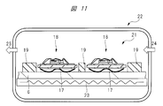
- FIG. 1 is a cross-sectional view of the semiconductor device SD of the present embodiment. Since each of the six arms has the same structure, FIG. 1 shows one arm.
- the semiconductor device SD includes a chip (IGBT) 1, a chip (diode) 2, a ceramic substrate 3, a base substrate 6, an external terminal 8, and a sealing body 9.
- the chip 1 has a power semiconductor element such as IGBT formed on a substrate made of silicon (Si) or silicon carbide (SiC).
- the chip 2 has a substrate made of silicon (Si) or silicon carbide (SiC). A diode element is formed.
- the ceramic substrate 3 has a substrate 3a, a front surface (first surface) 3t of the substrate 3a, and a back surface (second surface) 3b located on the opposite side of the front surface 3t.
- the wiring 3c is formed, and the surface of the wiring 3c is covered with a plating layer (metal layer) 3d. Note that the wiring 3c and the plating layer 3d may be collectively called a wiring.
- the substrate 3a can be made of, for example, aluminum nitride (AlN) or silicon nitride (Si 3 N 4 ) having high thermal conductivity, or alumina (Al 2 O 3 ) having high versatility.
- the wiring 3c can be, for example, a copper (Cu) film
- the plating layer 3d can be, for example, a nickel (Ni) film.
- the chip 1 and the chip 2 are bonded to the plating layer 3d on the ceramic substrate 3 via the bonding layer 4, and are electrically connected to the wiring 3c and the plating layer 3d.
- the chip 1 and the chip 2 are connected to each other via a wire 5 and are connected to the wiring 3c via the wire 5.
- an external terminal 8 is connected to the wiring 3c and the plating layer 3d. That is, the chips 1 and 2 are electrically connected to the external terminals 8.
- the wire 5 is made of, for example, a copper (Cu) wire or an aluminum (Al) wire.
- the base substrate 6 includes a substrate 6a, a front surface (first surface) 6t of the substrate 6a, a back surface (second surface) 6b located on the side opposite to the front surface 6t, and plating formed on the front surface 6t and the back surface 6b.
- the substrate 6a is made of, for example, a composite material (AlSiC) of silicon carbide (SiC) having a high thermal conductivity and an aluminum (Al) alloy, copper (Cu), or an aluminum (Al) alloy, and has a plating layer 6c. Is made of, for example, a nickel (Ni) film.
- the wiring 3c and the plating layer 3d formed on the back surface 3b of the ceramic substrate 3 are connected to the plating layer 6c formed on the front surface 6t of the base substrate 6 via the adhesive layer 7.
- the adhesive layers 4 and 7 are solder materials, for example, a Sn (Pb) solder material containing lead (Pb), or a solder material made of a so-called lead-free solder substantially containing no Pb.
- the lead-free solder include tin-copper-silver (Sn-Cu-Ag), tin-copper (Sn-Cu), tin-antimony (Sn-Sb), or tin-copper-antimony (Sn-Cu). —Sb) and the like.
- the chip 1, the chip 2, the ceramic substrate 3, the wires 5, the adhesive layer 4, the adhesive layer 7, and the external terminals 8 are covered with a sealing body 9.
- the sealing body 9 is made of, for example, silicone gel. Although not shown, the external terminals are exposed outside the sealing body 9.
- FIG. 2 is a manufacturing process flow chart showing a part of the method of manufacturing the semiconductor device of the present embodiment.
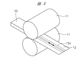
- FIG. 3 is a perspective view showing the manufacturing process of the solder sheet of the present embodiment.
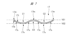
- FIGS. 6 is a perspective view of the solder sheet of the present embodiment, and
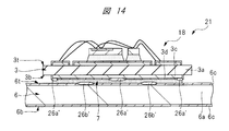
- FIG. 7 is a cross-sectional view along X1-X1 in FIG. 8 to 14 are cross-sectional views of the semiconductor device during the manufacturing process.
- either of the solder sheet 17 preparing step S1 and the first laminate 18 preparing step may be performed first.
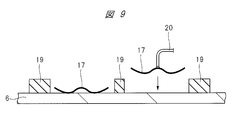
- 9 to 11 show two arm regions on the base substrate 6.
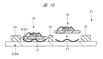
- FIG. 12 shows the preheating step
- FIGS. 13 and 14 show the main heating step, but shows the second laminated body 21 for one arm, and omits a heating device such as a chamber. .
- solder sheet 17 preparing step S1 shown in FIG. 2 will be described.
- a solder ingot 10 having a thickness of, for example, 2 mm is rolled to a thickness of, for example, 0.2 mm by a pair of rolling rolls 11 to form a rolled solder 12.
- fine irregularities called rolled eyes 12a are formed.
- a rectangular pre-press solder sheet 15 is formed using the die 13 and the punch 14.
- the pre-press solder sheet 15 is, for example, 47 ⁇ 57 mm.
- the pre-press solder sheet 15 is sandwiched between a pair of dies 16 and subjected to compression processing into a desired shape to form a solder sheet 17.
- the solder sheet 17 has a W-shaped cross section. As shown in FIG. 6, the solder sheet 17 has a front surface (first surface) 17t and a back surface (second surface) 17b located on the opposite side of the front surface 17t.
- the surface 17t has two sides 17x1 and 17x2 extending in the X direction and two sides 17y1 and 17y2 extending in the Y direction.
- the front surface 17t has concave portions C1 and C2
- the back surface 17b has concave portions C3, and the concave portions C1 to C3 extend continuously in the Y direction inside the solder sheet 17, and have the sides 17x1 and At 17 ⁇ 2, it reaches the outside of the solder sheet 17.
- the front surface 17t and the back surface 17b of the solder sheet 17 have flat surfaces by the compression processing shown in FIG. That is, the roll 12a # formed by the rolling process shown in FIG. 3 is crushed by the compression process shown in FIG. 5, and the surface areas of the front surface 17t and the back surface 17b are the same as those of the pre-press solder sheet 15 shown in FIG. And it is smaller than the surface area of the back surface.
- a suction portion 17a having a flat surface is provided.
- the solder sheet 17 has three ridges 17m and two valleys 17v, and has a straight portion 17s between the ridges 17m and the valleys 17v.
- the peaks 17m and the valleys 17v are regions in which plastic deformation has been performed from a straight line into an arc shape by the compression processing, but the straight line portions 17s are not plastically deformed. Therefore, the peak portion 17m and the valley portion 17v have higher hardness than the straight portion 17s due to work hardening. Further, the film thickness of the peak portion 17m and the valley portion 17v is larger than the film thickness of the linear portion 17s. Also, since the three peaks 17m are set at the same height, they contact the virtual plane VS1.
- the two valleys 17v are also set to the same height, they contact the virtual plane VS2.
- the virtual plane VS1 corresponds to a plating layer 3d of the ceramic substrate 3 shown in FIG. 10 described later
- the virtual plane VS2 corresponds to the plating layer 6c of the base substrate 6 (the plating layers 3d and 6c are Shown in FIG. 1).
- a first laminate 18 preparing step shown in FIG. 2 is performed. Specifically, there are a step S2 for mounting the chips 1 and 2 on the ceramic substrate 3 and a wire bonding step S3. As shown in FIG. 8, the chips 1 and 2 are mounted on the ceramic substrate 3 and bonded to the wiring 3c via the bonding layer 4. Next, the wires 5 electrically connect between the chip 1 and the chip 2, between the wiring 3c and the chip 1, and between the wiring 3c and the chip 2, respectively.
- the second laminate 21 preparing step S4 shown in FIG. 2 is performed.
- the solder sheets 17 are sequentially placed on a plurality of regions surrounded by the guides 19 on the base substrate 6.
- the solder sheet 17 has a flat suction portion 17a, and the suction portion 17a is vacuum-sucked by the suction jig 20, and the solder sheet 17 is placed on the base substrate 6.
- the guide 19 positions the formation area of each arm.
- the first stacked body 18 is sequentially placed on the solder sheet 17, and the plurality of first stacked bodies 18 are placed on the base substrate 6 via the solder sheet 17.
- a two-layered body 21 is prepared.
- the concave portions C1 to C3 shown in FIGS. 6 and 7 are secured without being crushed.
- the concave portions C1 to C3 are secured without being crushed until a preheating step S6 described later is completed.
- Sn-10% Sb having a melting point of about 250 ° C. is used as the solder material of the solder sheet 17.
- a step S5 of setting the second stacked body 21 in the chamber 22 shown in FIG. 2 is performed.
- the second laminate 21 is set inside the chamber 22 of the heat treatment apparatus for solder connection.
- a preheating step S6 and a main heating step S7 which will be described later, are performed.
- the heat treatment apparatus includes a chamber 22, a heating mechanism 23, a gas introduction mechanism 24, and an exhaust mechanism 25.
- the pressure in the chamber 22 is reduced to, for example, about 300 Pa, and then, for example, nitrogen (N 2 ) is supplied in the chamber 22. Then, the inside of the chamber 22 is returned to the atmospheric pressure. Thus, the inside of the chamber 22 is set to a pure nitrogen (N 2 ) atmosphere.
- a preheating step S6 shown in FIG. 2 is performed.
- the second laminate 21 is heated while supplying a mixed gas of formic acid and nitrogen (N 2 ) into the chamber 22.
- the heating temperature is 200 ° C. lower than the melting point of the solder material of the solder sheet 17, and the heating time is about 10 minutes.
- the surface oxide film of the solder sheet 17 and the surface oxide films of the plating layers 3d and 6c are removed by utilizing the reduction reaction of formic acid. It is known that formic acid efficiently causes a reduction reaction at about 150 ° C. or higher.
- the solder sheet 17 is in contact with the plating layer 3d formed on the surface of the wiring 3c of the ceramic substrate 3 at the three peaks 17m, and at the two valleys 17v. Is in contact with the plating layer 6c formed on the surface of.
- Two concave portions C1 and C2 are provided on the front surface 17t of the solder sheet 17, and a concave portion C3 is provided on the back surface 17b of the solder sheet 17. Then, as shown in FIGS. 6 and 7, the concave portions C1 to C3 extend continuously inside the solder sheet 17 and reach the outside of the solder sheet 17 in plan view.
- solder sheet 17 is in contact with the plating layer 3d of the ceramic substrate 3 at a plurality of peaks 17m and in contact with the plating layer 6c of the base substrate 6 at a plurality of valleys 17v in cross-sectional view, the first The first laminate 18 can be supported without the concave portions C1 to C3 being crushed by the weight of the laminate 18.
- FIG. 13 shows a state when the melting of the solder material of the solder sheet 17 is started
- FIG. 14 shows a state after the melting of the solder material and when the solder material is solidified.
- the reaction layer 26 a is formed of a tin-nickel alloy (Sn—Ni alloy) of tin (Sn) contained in the solder material of the solder sheet 17 and nickel (Ni) contained in the plating layer 3 d, or a solder material of the solder sheet 17. It is a tin-copper alloy (Sn-Cu alloy) of tin (Sn) contained therein and copper (Cu) contained in the wiring 3c.
- the reaction layer 26b is a tin-nickel alloy (Sn-Ni alloy) of tin (Sn) contained in the solder material of the solder sheet 17 and nickel (Ni) contained in the plating layer 6c.
- the first laminate 18 descends to the base substrate 6 side, and as shown in FIG. Interval becomes narrower.
- the pressure inside the chamber 22 (see FIG. 11) is reduced to, for example, about 300 Pa to remove voids remaining in the molten solder layer.
- nitrogen (N 2 ) is introduced into the chamber 22 (see FIG. 11) to solidify the molten solder layer.
- the first laminate 18 is bonded to the base substrate 6 with the bonding layer 7 made of a solder layer.
- reaction layer 26a 'and 26b' are formed by growing the above-described reaction layers 26a and 26b, and the thickness of the reaction layers 26a 'and 26b' is larger than the thickness of the reaction layers 26a and 26b.
- the removal step S8 of the second laminate 21 shown in FIG. 2, the external terminal 8 connection step S9, and the sealing body 9 formation step S10 are performed.
- the cooled second laminate 21 is taken out of the chamber 22 (see FIG. 11), and the external terminals 8 are connected to the wiring 3c and the plating layer 3d formed on the ceramic substrate 3 as shown in FIG. Connect to Next, on the surface 6t side of the base substrate 6, the chip 1, the chip 2, the ceramic substrate 3, the wires 5, the adhesive layer 4, the adhesive layer 7, and the external terminals 8 are covered with a sealing body 9, and the semiconductor device shown in FIG. SD is completed.
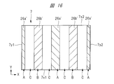
- FIG. 15 is an enlarged cross-sectional view of a main part in FIG.
- FIG. 16 is a plan view of the bonding layer 7 of FIG. 15, and
- FIG. 17 is an enlarged sectional view of a main part of a semiconductor device as a comparative example.
- the ceramic substrate 3 and the base substrate 6 are bonded by an adhesive layer 7 made of a solder layer.
- a relatively thick reaction layer 26a 'and a relatively thin reaction layer 26c are formed at the interface between the adhesive layer 7 and the plating layer 3d of the ceramic substrate 3.
- the reaction layer 26c is formed in a region between the plurality of reaction layers 26a '.
- a relatively thick reaction layer 26b 'and a relatively thin reaction layer 26d are formed at the interface between the adhesive layer 7 and the plating layer 6c of the base substrate 6, a relatively thick reaction layer 26b 'and a relatively thin reaction layer 26d are formed.
- the reaction layer 26d is formed in a region between the plurality of reaction layers 26b '.
- the relatively thick reaction layers 26a 'and 26b' have a thickness of about 50 ⁇ m
- the relatively thin reaction layers 26c and 26d have a thickness of about 20 ⁇ m.
- the adhesive layer 7 made of a solder layer is rectangular and has two sides 7x1 and 7x2 extending in the X direction and sides 7y1 and 7y2 extending in the Y direction. .
- the region where the reaction layer 26a 'is formed is referred to as a region A
- the region where the reaction layer 26b' is formed is referred to as a region B
- the region between the region A and the region B is referred to as a region C.
- the regions A, B and C extend continuously in the Y direction from the side 7x1 extending in the X direction to the side 7x2. Focusing on the interface between the adhesive layer 7 and the plating layer 3d shown in FIG.
- reaction layer 26a ' is formed in the region A shown in FIG. 16, and the reaction layer 26c is formed in the regions B and C.
- the areas B and C have larger areas than the area A.
- reaction layer 26b ' is formed in the region B shown in FIG. 16, and the reaction layer 26d is formed in the regions A and C. .
- the areas A and C are larger than the area B.
- the formation region of the relatively thick reaction layers 26a 'and 26b' is the region where the solder sheet 17 and the plating layers 3d and 6c are in contact, and the relatively thin reaction layers 26c and 26b '
- the formation region of 26d is a region where the solder sheet 17 and the plating layers 3d and 6c are out of contact with each other.
- FIG. 17 is an enlarged cross-sectional view of a main part of a semiconductor device as a comparative example, and corresponds to FIG. FIG. 17 shows an example using a V-shaped solder sheet disclosed in the prior art document.
- a V-shaped solder sheet is used, the solder sheet is crushed and flattened by the weight of the first stacked body in the second stacked body preparing step S4 of the above embodiment. Then, in a state where the solder sheet and the plating layer 3d or 6c to be joined are in close contact with each other, the preheating step S6 is performed, but formic acid is sufficiently penetrated into the interface between the solder sheet and the plating layer 3d or 6c.
- the thick reaction layers 26e and 26f are formed in almost the entire area of the interface, the mechanical strength of the adhesive layer 7 is reduced, and the life is shortened due to cracks generated by the stress applied to the adhesive layer 7. Probability is high. In particular, if the product is continued to be used, the reaction layers 26e and 26f gradually grow and increase in thickness, and conversely, the thickness of the solder layer of the adhesive layer 7 decreases, so that cracks are more likely to occur. . Therefore, the product life is shorter than in this embodiment.
- the solder sheet 17 has concave portions C1 to C3 on the front surface 17t and the rear surface 17b, and the concave portions C1 to C3 continuously extend inside the solder sheet 17 in plan view. 17, the formic acid can penetrate into the concave portions C1 to C3. Since the surface oxide film formed on each of the solder sheet 17, the plating layer 3d on the ceramic substrate 3 side, and the plating layer 6c on the base substrate 6 side can be removed, wetting of the solder material of the solder sheet 17 can be achieved. The heat resistance of the adhesive layer 7 made of a solder layer can be reduced. That is, a semiconductor device (power module) with high heat dissipation can be provided.
- the pressure inside the chamber 22 is reduced, so that residual voids can be reduced, and the thermal resistance of the adhesive layer 7 made of a solder layer can be reduced. Can be.
- a relatively thick reaction layer 26a 'and a relatively thin reaction layer 26c are formed at the interface between the adhesive layer 7 and the plating layer 3d on the ceramic substrate 3 side.
- the mechanical strength of the adhesive layer 7 can be improved as compared with the comparative example in which a relatively thick reaction layer 26e is formed entirely on the interface between the adhesive layer 7 and the plating layer 3d on the ceramic substrate 3 side. Cracks caused by stress applied to the layer 7 can be prevented. Further, the product life of the semiconductor device can be extended. The same applies to the interface between the adhesive layer 7 and the plating layer 6c of the base substrate 6.
- the solder sheet 17 has a recess C1 on the front surface 17t and a recess C3 on the back surface 17b. Then, as shown in FIG. 12, the solder sheet 17 comes into contact with the plating layer 3d of the ceramic substrate 3 at the peaks 17m located at both ends of the concave portion C1 and the valleys located at both ends of the concave portion C3 in cross-sectional view. Since the portion 17v is in contact with the plating layer 6c of the base substrate 6, the first laminate 18 can be supported without the concave portions C1 and C3 being crushed by the weight of the first laminate 18.
- the solder sheet 17 has a W-shape, and the peaks 17m and the valleys 17v plastically deformed in an arc shape have increased in hardness due to work hardening. The strength in the direction has been improved. Therefore, even when the first laminate 18 is placed on the solder sheet 17, the first laminate 18 can be supported without the concave portions C1 and C3 being crushed by the weight of the first laminate 18.
- FIG. 18 is a perspective view of a solder sheet according to Modification Example 1, and FIG. 19 is a cross-sectional view along X2-X2 in FIG.
- the solder sheet 27 of the first modification has an N-shape in a cross-sectional view.
- the solder sheet 27 has a front surface (first surface) 27t and a back surface (second surface) 27b opposite to the front surface 27t.
- the surface 27t has two sides 27x1 and 27x2 extending in the X direction and two sides 27y1 and 27y2 extending in the Y direction.
- the front surface 27t has a concave portion C4, the back surface 27b has a concave portion C5, and the concave portions C4 and C5 extend continuously in the Y direction inside the solder sheet 27, and extend along the sides 27x1 and 27x2. It reaches the outside of the solder sheet 27.
- the solder sheet 27 has two ridges 27m and two valleys 27v, and has a linear portion 27s between the ridges 27m and the valleys 27v.
- the peaks 27m and the valleys 27v are regions where plastic deformation has been performed from a straight line into an arc by the above-described compression processing, but the linear portion 27s is not plastically deformed. Therefore, the peaks 27m and the valleys 27v have a higher hardness than the linear portions 27s due to work hardening. Since the two peaks 27m are set at the same height, they contact the virtual plane VS1. Similarly, since the two valleys 27v are also set to the same height, they contact the virtual plane VS2.
- the virtual plane VS1 corresponds to the plating layer 3d of the ceramic substrate 3 shown in FIG. 10, and the virtual plane VS2 corresponds to the plating layer 6c of the base substrate 6 (the plating layers 3d and 6c correspond to FIG. Shown).
- solder sheet 17 is replaced with a solder sheet 27.
- the solder sheet 27 has a recess C4 on the front surface 27t and a recess C5 on the back surface 27b. Then, the solder sheet 27 contacts the plating layer 3d of the ceramic substrate 3 at the ridges 27m located at both ends of the concave portion C4 and the valley portions 27v located at both ends of the concave portion C5. Since the first laminate 18 is in contact with the plating layer 6c, the first laminate 18 can be supported without the concave portions C4 and C5 being crushed by the weight of the first laminate 18. Therefore, according to the solder sheet 27 of the first modification, the same effect as that of the above embodiment can be achieved.
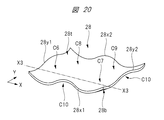
- FIG. 20 is a perspective view of a solder sheet according to Modification Example 2, and FIG. 19 is a cross-sectional view along X2-X2 in FIG.
- the solder sheet 28 of Modification 2 has the W-shaped cross-sectional structure of the above embodiment in the X direction and the Y direction.
- the solder sheet 28 has a front surface (first surface) 28t and a back surface (second surface) 28b located on the opposite side of the front surface 28t.
- the surface 28t has two sides 28x1 and 28x2 extending in the X direction and two sides 28y1 and 28y2 extending in the Y direction.
- the front surface 28t has concave portions C6 to C9
- the rear surface 28b # has a concave portion C10
- the concave portion C6 is formed inside the solder sheet 28 and reaches the outside of the solder sheet 28 at sides 28x1 and 28y1. I have.
- the recess C7 is formed inside the solder sheet 28 and reaches the outside of the solder sheet 28 at sides 28x1 and 28y2, and the recess C8 is formed inside the solder sheet 28 and the solder sheet 28 at the sides 28x2 and 28y1.
- the concave portion C9 is formed inside the solder sheet 28 and reaches the outside of the solder sheet 28 at sides 28x2 and 28y2.
- the concave portion C10 extends continuously in the X direction and the Y direction inside the solder sheet 28, and reaches the outside of the solder sheet 28 at sides 28x1, 28x2, 28y1, and 28y2.
- the present invention is not limited to the embodiments described above, but includes various modifications.
- the above-described embodiments have been described in detail in order to easily explain the present invention, and are not necessarily limited to those having all the configurations described above.
- a part of the configuration of one embodiment can be replaced with the configuration of another embodiment, and the configuration of one embodiment can be added to the configuration of another embodiment.
- formic acid is used as the reducing gas, but hydrogen may be used.
Landscapes
- Engineering & Computer Science (AREA)
- Mechanical Engineering (AREA)
- Microelectronics & Electronic Packaging (AREA)
- Die Bonding (AREA)
- Structure Of Printed Boards (AREA)
- Cooling Or The Like Of Semiconductors Or Solid State Devices (AREA)
Abstract
L'invention concerne un procédé de fabrication d'un dispositif à semi-conducteur comprenant : une étape de préparation d'un second stratifié qui est obtenu par montage d'un premier stratifié sur un substrat de base par l'intermédiaire d'une feuille de brasage ; une étape d'installation du second stratifié à l'intérieur d'une chambre et de préchauffage du second stratifié à une température égale ou inférieure à un point de fusion de brasure de la feuille de brasage tout en introduisant un gaz réducteur dans la chambre ; et une étape de chauffage du second stratifié à une température égale ou supérieure au point de fusion de la brasure de la feuille de brasage. La feuille de brasage comprend une partie évidée (C1) sur un côté substrat céramique et une partie évidée (C3) sur un côté substrat de base, et dans l'étape de préchauffage, la feuille de brasage est en contact avec une couche plaquée aux deux extrémités de la partie évidée (C1) et est en contact avec la couche plaquée aux deux extrémités de la partie évidée (C3). Dans une vue en plan, la partie évidée (C1) et la partie évidée (C3) s'étendent en continu à l'intérieur de la feuille de brasage vers l'extérieur de la feuille de brasage.
Applications Claiming Priority (2)
| Application Number | Priority Date | Filing Date | Title |
|---|---|---|---|
| JP2018-141648 | 2018-07-27 | ||
| JP2018141648A JP6944907B2 (ja) | 2018-07-27 | 2018-07-27 | 半導体装置の製造方法および半導体装置ならびに半田シートおよびその製造方法 |
Publications (1)
| Publication Number | Publication Date |
|---|---|
| WO2020021760A1 true WO2020021760A1 (fr) | 2020-01-30 |
Family
ID=69180878
Family Applications (1)
| Application Number | Title | Priority Date | Filing Date |
|---|---|---|---|
| PCT/JP2019/010159 Ceased WO2020021760A1 (fr) | 2018-07-27 | 2019-03-13 | Procédé de fabrication de dispositif à semi-conducteur, dispositif à semi-conducteur, feuille de brasage et son procédé de fabrication |
Country Status (2)
| Country | Link |
|---|---|
| JP (1) | JP6944907B2 (fr) |
| WO (1) | WO2020021760A1 (fr) |
Cited By (1)
| Publication number | Priority date | Publication date | Assignee | Title |
|---|---|---|---|---|
| DE102024201491A1 (de) * | 2024-02-19 | 2025-08-21 | Schaeffler Technologies AG & Co. KG | Verfahren zum Verlöten eines elektronischen Bauelements mit einer beschichteten Basis und elektronische Komponente für einen Inverter |
Families Citing this family (1)
| Publication number | Priority date | Publication date | Assignee | Title |
|---|---|---|---|---|
| JP2021158158A (ja) * | 2020-03-25 | 2021-10-07 | 株式会社鈴野製作所 | はんだ付け方法、はんだ付け装置およびシートはんだ |
Citations (4)
| Publication number | Priority date | Publication date | Assignee | Title |
|---|---|---|---|---|
| JPH03254393A (ja) * | 1990-02-28 | 1991-11-13 | Taiyo Yuden Co Ltd | 溝付きシート状はんだおよびその製造方法 |
| JP2005271059A (ja) * | 2004-03-26 | 2005-10-06 | Toyota Motor Corp | 接合構造体および接合構造体の製造方法 |
| JP2009272554A (ja) * | 2008-05-09 | 2009-11-19 | Honda Motor Co Ltd | ハンダ付け方法 |
| JP6355092B1 (ja) * | 2017-05-11 | 2018-07-11 | パナソニックIpマネジメント株式会社 | はんだ合金およびそれを用いた接合構造体 |
-
2018
- 2018-07-27 JP JP2018141648A patent/JP6944907B2/ja active Active
-
2019
- 2019-03-13 WO PCT/JP2019/010159 patent/WO2020021760A1/fr not_active Ceased
Patent Citations (4)
| Publication number | Priority date | Publication date | Assignee | Title |
|---|---|---|---|---|
| JPH03254393A (ja) * | 1990-02-28 | 1991-11-13 | Taiyo Yuden Co Ltd | 溝付きシート状はんだおよびその製造方法 |
| JP2005271059A (ja) * | 2004-03-26 | 2005-10-06 | Toyota Motor Corp | 接合構造体および接合構造体の製造方法 |
| JP2009272554A (ja) * | 2008-05-09 | 2009-11-19 | Honda Motor Co Ltd | ハンダ付け方法 |
| JP6355092B1 (ja) * | 2017-05-11 | 2018-07-11 | パナソニックIpマネジメント株式会社 | はんだ合金およびそれを用いた接合構造体 |
Cited By (1)
| Publication number | Priority date | Publication date | Assignee | Title |
|---|---|---|---|---|
| DE102024201491A1 (de) * | 2024-02-19 | 2025-08-21 | Schaeffler Technologies AG & Co. KG | Verfahren zum Verlöten eines elektronischen Bauelements mit einer beschichteten Basis und elektronische Komponente für einen Inverter |
Also Published As
| Publication number | Publication date |
|---|---|
| JP6944907B2 (ja) | 2021-10-06 |
| JP2020017707A (ja) | 2020-01-30 |
Similar Documents
| Publication | Publication Date | Title |
|---|---|---|
| JP7535606B2 (ja) | パワー半導体装置およびその製造方法 | |
| KR102459745B1 (ko) | 구리/세라믹스 접합체, 절연 회로 기판, 및, 구리/세라믹스 접합체의 제조 방법, 절연 회로 기판의 제조 방법 | |
| US8772926B2 (en) | Production method of cooler | |
| US9818716B2 (en) | Power module | |
| JP6944907B2 (ja) | 半導体装置の製造方法および半導体装置ならびに半田シートおよびその製造方法 | |
| JP2014120639A (ja) | パワーモジュール半導体装置 | |
| US20240055392A1 (en) | Method of manufacturing semiconductor device | |
| JP2014053403A (ja) | パワーモジュール半導体装置 | |
| EP3845511B1 (fr) | Corps assemblé en cuivre/céramique, carte de circuit imprimé isolée, procédé de production de corps assemblé en cuivre/céramique, et procédé de fabrication de carte de circuit imprimé isolée | |
| EP2765597A2 (fr) | Système de frittage utilisant un gas ou liquide sous pression | |
| JP7487614B2 (ja) | 半導体装置、半導体装置の製造方法及び電力変換装置 | |
| JP6939973B2 (ja) | 銅/セラミックス接合体、及び、絶縁回路基板 | |
| KR20230087833A (ko) | 양면 냉각형 파워모듈 제조 방법 및 양면 냉각형 파워모듈 | |
| JP2013175697A (ja) | 半導体装置およびその製造方法 | |
| JP7750825B2 (ja) | パワー半導体モジュールおよびその形成方法 | |
| JP2019087608A (ja) | 接合体、絶縁回路基板、ヒートシンク付絶縁回路基板、ヒートシンク、及び、接合体の製造方法、絶縁回路基板の製造方法、ヒートシンク付絶縁回路基板の製造方法、ヒートシンクの製造方法 | |
| JP2022029886A (ja) | 半導体装置、半導体装置の製造方法及び電力変換装置 | |
| WO2024058211A1 (fr) | Fil de liaison en cuivre, procédé de fabrication de fil de liaison en cuivre et dispositif à semi-conducteur | |
| JP4121827B2 (ja) | モジュール構造体の製造方法 | |
| EP4513547A1 (fr) | Substrat de circuit en céramique, dispositif à semi-conducteur, procédé de fabrication de substrat de circuit en céramique et procédé de fabrication de dispositif à semi-conducteur | |
| JP7135951B2 (ja) | 絶縁回路基板の製造方法 | |
| JP2020013915A (ja) | ヒートシンク付き絶縁回路基板の製造方法及びヒートシンク付き絶縁回路基板 | |
| CN120767259A (zh) | 一种功率半导体芯片压接封装结构及制作方法 | |
| JP2023084727A (ja) | シート状はんだ | |
| TW202534705A (zh) | 銅接合帶、銅接合帶之製造方法及半導體裝置 |
Legal Events
| Date | Code | Title | Description |
|---|---|---|---|
| 121 | Ep: the epo has been informed by wipo that ep was designated in this application |
Ref document number: 19841986 Country of ref document: EP Kind code of ref document: A1 |
|
| NENP | Non-entry into the national phase |
Ref country code: DE |
|
| 122 | Ep: pct application non-entry in european phase |
Ref document number: 19841986 Country of ref document: EP Kind code of ref document: A1 |