WO2020031273A1 - ヒ化ガリウム単結晶体およびヒ化ガリウム単結晶基板 - Google Patents
ヒ化ガリウム単結晶体およびヒ化ガリウム単結晶基板 Download PDFInfo
- Publication number
- WO2020031273A1 WO2020031273A1 PCT/JP2018/029679 JP2018029679W WO2020031273A1 WO 2020031273 A1 WO2020031273 A1 WO 2020031273A1 JP 2018029679 W JP2018029679 W JP 2018029679W WO 2020031273 A1 WO2020031273 A1 WO 2020031273A1
- Authority
- WO
- WIPO (PCT)
- Prior art keywords
- single crystal
- gaas single
- gaas
- outer peripheral
- gallium arsenide
- Prior art date
- Legal status (The legal status is an assumption and is not a legal conclusion. Google has not performed a legal analysis and makes no representation as to the accuracy of the status listed.)
- Ceased
Links
Images


Classifications
-
- C—CHEMISTRY; METALLURGY
- C30—CRYSTAL GROWTH
- C30B—SINGLE-CRYSTAL GROWTH; UNIDIRECTIONAL SOLIDIFICATION OF EUTECTIC MATERIAL OR UNIDIRECTIONAL DEMIXING OF EUTECTOID MATERIAL; REFINING BY ZONE-MELTING OF MATERIAL; PRODUCTION OF A HOMOGENEOUS POLYCRYSTALLINE MATERIAL WITH DEFINED STRUCTURE; SINGLE CRYSTALS OR HOMOGENEOUS POLYCRYSTALLINE MATERIAL WITH DEFINED STRUCTURE; AFTER-TREATMENT OF SINGLE CRYSTALS OR A HOMOGENEOUS POLYCRYSTALLINE MATERIAL WITH DEFINED STRUCTURE; APPARATUS THEREFOR
- C30B11/00—Single-crystal growth by normal freezing or freezing under temperature gradient, e.g. Bridgman-Stockbarger method
- C30B11/003—Heating or cooling of the melt or the crystallised material
-
- C—CHEMISTRY; METALLURGY
- C30—CRYSTAL GROWTH
- C30B—SINGLE-CRYSTAL GROWTH; UNIDIRECTIONAL SOLIDIFICATION OF EUTECTIC MATERIAL OR UNIDIRECTIONAL DEMIXING OF EUTECTOID MATERIAL; REFINING BY ZONE-MELTING OF MATERIAL; PRODUCTION OF A HOMOGENEOUS POLYCRYSTALLINE MATERIAL WITH DEFINED STRUCTURE; SINGLE CRYSTALS OR HOMOGENEOUS POLYCRYSTALLINE MATERIAL WITH DEFINED STRUCTURE; AFTER-TREATMENT OF SINGLE CRYSTALS OR A HOMOGENEOUS POLYCRYSTALLINE MATERIAL WITH DEFINED STRUCTURE; APPARATUS THEREFOR
- C30B11/00—Single-crystal growth by normal freezing or freezing under temperature gradient, e.g. Bridgman-Stockbarger method
-
- C—CHEMISTRY; METALLURGY
- C30—CRYSTAL GROWTH
- C30B—SINGLE-CRYSTAL GROWTH; UNIDIRECTIONAL SOLIDIFICATION OF EUTECTIC MATERIAL OR UNIDIRECTIONAL DEMIXING OF EUTECTOID MATERIAL; REFINING BY ZONE-MELTING OF MATERIAL; PRODUCTION OF A HOMOGENEOUS POLYCRYSTALLINE MATERIAL WITH DEFINED STRUCTURE; SINGLE CRYSTALS OR HOMOGENEOUS POLYCRYSTALLINE MATERIAL WITH DEFINED STRUCTURE; AFTER-TREATMENT OF SINGLE CRYSTALS OR A HOMOGENEOUS POLYCRYSTALLINE MATERIAL WITH DEFINED STRUCTURE; APPARATUS THEREFOR
- C30B29/00—Single crystals or homogeneous polycrystalline material with defined structure characterised by the material or by their shape
- C30B29/10—Inorganic compounds or compositions
- C30B29/40—AIIIBV compounds wherein A is B, Al, Ga, In or Tl and B is N, P, As, Sb or Bi
- C30B29/42—Gallium arsenide
Definitions
- the present disclosure relates to a gallium arsenide single crystal and a gallium arsenide single crystal substrate.
- GaAs (gallium arsenide) single crystal has been proposed as a substrate for a light emitting device and an electronic device, from the viewpoint of growing a semiconductor layer of high crystal quality thereon, with a small residual strain.
- Patent Document 1 discloses that in a heat treatment of a GaAs crystal obtained by a vertical Bridgeman method, a temperature change during a temperature rise or a cooling process is 300 ° C./hour or less in a temperature range of 600 ° C. or less. A temperature of 600 ° C. to 750 ° C., 150 ° C./hour or less, a temperature range of 750 ° C. to heat treatment temperature of 50 ° C./hour or less, and a temperature of 800 ° C. to 1000 ° C. for 1 to 100 hours. Discloses that a GaAs crystal having an average of the magnitude of the residual strain obtained by photoelasticity measurement of less than 1 ⁇ 10 ⁇ 5 can be obtained.
- Patent Document 2 discloses a solid phase forming a GaAs single crystal during the production of a GaAs single crystal by LEC (liquid sealed Czochralski) method and a liquid phase composed of a GaAs melt.
- the shape of the solid phase at the liquid interface is convex on the liquid phase side, and the convexity (the length T1 from the interface between the GaAs melt and the liquid sealant to the tip of the convexity and the GaAs single crystal
- the ratio T1 / T2 to the outer diameter T2) is 0.25 or more
- the crystal growth rate V1 in the relative movement direction of the solid-liquid interface is 4 mm / hour to 7 mm / hour
- the solid phase cooling rate V2 is 5 ° C. / Hr or less
- the absolute value of the residual strain in the plane of the wafer is less than 1.0 ⁇ 10 ⁇ 5 at the center of the plane and 1.0 ⁇ 10 ⁇ 5 or more at the outer periphery of the plane. in it the [011] direction of the region and the outer peripheral portion 1.0 ⁇ 10 below -5 Discloses that GaAs single crystal wafer having a certain area is obtained.
- the gallium arsenide single crystal according to an aspect of the present disclosure includes a cylindrical straight body, and is 10 mm outside from the inner circumference toward the center axis from the outer circumference of the straight body and 5 mm inside from the outer circumference.
- the residual strain in the tangential direction at the outer peripheral portion up to is the compressive strain.
- the tangential residual strain in the outer peripheral portion from the outer periphery to the inner periphery of 10 mm from the outer periphery toward the center and 5 mm inward from the outer periphery is the compressive strain.
- FIG. 1 is a schematic plan view showing a gallium arsenide single crystal according to an embodiment of the present disclosure.
- FIG. 2 is a schematic sectional view showing a typical gallium arsenide single crystal manufacturing apparatus and method.
- FIG. 3 is a schematic cross-sectional view showing a gallium arsenide single crystal manufacturing apparatus and method according to an embodiment of the present disclosure.
- FIG. 4A is a graph illustrating an example of a relationship between a temperature difference and a stress in a single crystal body when the gallium arsenide single crystal body is cooled by a typical method.
- FIG. 4A is a graph illustrating an example of a relationship between a temperature difference and a stress in a single crystal body when the gallium arsenide single crystal body is cooled by a typical method.
- FIG. 4B shows another example of the relationship between the temperature difference and the stress in the single crystal when the single crystal of gallium arsenide is cooled by a typical method in which the temperature difference in the longitudinal direction of the single crystal is reduced. It is a graph.
- FIG. 4C is a graph showing an example of the relationship between the temperature difference in the single crystal and the strain when the gallium arsenide single crystal is cooled by a typical method in which the temperature difference in the longitudinal direction of the single crystal is reduced. It is.
- FIG. 5 is a graph showing an example of a relationship between a temperature difference and a strain in a single crystal body when the gallium arsenide single crystal body is cooled by a method according to an embodiment of the present disclosure.
- FIG. 6 is a schematic plan view showing a gallium arsenide single crystal substrate according to another aspect of the present disclosure.
- a GaAs crystal disclosed in JP-A-11-268997 (Patent Document 1) or a GaAs single crystal wafer disclosed in JP-A-2012-236750 (Patent Document 2) is grown when a semiconductor layer is grown thereon.
- the rate of temperature rise to the temperature is high, there is a problem that a slip occurs in the GaAs crystal or the GaAs single crystal wafer.
- the slip is observed when the dislocation moves easily in a slip system.
- the slip occurs on a mirror-polished single crystal wafer, the slip is calculated as a step on the GaAs single crystal wafer surface. Observed with an interference microscope and, if significant, also visually.
- a gallium arsenide single crystal according to an aspect of the present disclosure includes a columnar straight body, and an outer face and an outer face from an inner face of 10 mm from the outer face of the straight body toward the central axis.
- the residual strain in the tangential direction in the outer peripheral portion from the inside to the inside of 5 mm is compression strain.
- the generation of a slip when a semiconductor layer is grown thereon is suppressed.
- of the difference between the radial strain component Sr and the tangential strain component St is measured at the outer peripheral portion.
- the average value can be not less than 2.5 ⁇ 10 ⁇ 6 and not more than 1.5 ⁇ 10 ⁇ 5 .
- Such a gallium arsenide single crystal further suppresses the occurrence of slip when a semiconductor layer is grown thereon.
- the diameter of the straight body can be 100 mm or more and 305 mm or less. Even in the case of such a gallium arsenide single crystal, the occurrence of slip is suppressed when a semiconductor layer is grown thereon.
- the gallium arsenide single crystal substrate according to another aspect of the present disclosure is characterized in that the tangential residual strain in the outer peripheral portion from the inner periphery of 10 mm toward the center from the outer periphery to the inner periphery of 5 mm from the outer periphery is compressive strain. It is. In the gallium arsenide single crystal substrate of this embodiment, generation of a slip when a semiconductor layer is grown thereon is suppressed.
- of the difference between the radial strain component Sr and the tangential strain component St in the outer peripheral portion The average value can be not less than 2.5 ⁇ 10 ⁇ 6 and not more than 1.5 ⁇ 10 ⁇ 5 . In such a gallium arsenide single crystal substrate, generation of a slip when a semiconductor layer is grown thereon is further suppressed.
- the gallium arsenide single crystal substrate can have a diameter of 100 mm or more and 305 mm or less. Even in the case of such a gallium arsenide single crystal substrate, generation of a slip when a semiconductor layer is grown thereon is suppressed.
- a GaAs single crystal body 10 (gallium arsenide single crystal body) of the present embodiment includes a cylindrical straight body part, and is 10 mm from an outer peripheral surface 10e of the straight body part toward a central axis 10o. Is the compressive strain in the tangential direction TD in the outer peripheral portion 10d outside the inner peripheral surface 10i and 5 mm inward from the outer peripheral surface 10e.
- the residual strain in the outer peripheral portion 10d of the GaAs single crystal body 10 refers to the residual strain at a point P arbitrarily specified in the outer peripheral portion 10d of the GaAs single crystal body 10.
- the direction of the residual strain is divided into a radial direction RD and a tangential direction TD.
- the radial direction RD is a direction of a radius connecting the central axis 10o and a point P arbitrarily specified.
- the tangential direction TD is a direction perpendicular to the radial direction at the point P, and is also called a circumferential direction.
- the types of residual strain include compression strain and tensile strain.
- the residual strain in the tangential direction TD at the outer peripheral portion 10d is a compressive strain
- the tensile force caused by the heat applied to the GaAs single crystal body 10 Since there is a compressive strain which is a strain in a direction of relaxing the stress, the occurrence of slip of the GaAs single crystal body 10 is suppressed.
- the residual strain of the GaAs single crystal body 10 is represented by the absolute value
- the in-plane distribution of the size is evaluated by a photoelastic method on a plane perpendicular to the mirror-finished central axis. With photoelasticity alone, it is not possible to specify the respective types (compression or tension) of the radial strain component Sr and the tangential strain component St of the residual strain.
- the type (compression or tension) of the radial strain component Sr and the tangential strain component St of the residual strain is evaluated by, for example, Raman shift by a Raman scattering spectrum on a plane perpendicular to the mirror-finished central axis of the GaAs single crystal. it can.
- the average value of the magnitude of the residual strain in the outer peripheral portion 10d of the GaAs single crystal body 10 is preferably from 2.5 ⁇ 10 ⁇ 6 to 1.5 ⁇ 10 ⁇ 5 .
- the magnitude of the residual strain in the outer peripheral portion 10d of the GaAs single crystal body 10 refers to the absolute value of the residual strain at a point specified arbitrarily in the outer peripheral portion 10d of the GaAs single crystal body 10.
- the average value of the magnitude of the residual strain refers to the average value of the magnitude of the residual strain at a plurality of points arbitrarily specified in the outer peripheral portion 10d of the GaAs single crystal body 10.
- the average value of the magnitude of the residual strain is calculated from the in-plane distribution evaluated by the photoelasticity method.
- the average value of the magnitude of the residual strain is preferably 2.5 ⁇ 10 ⁇ 6 or more, and 4.0 ⁇ 10 ⁇ 6 or more. Is more preferred.
- compression deformation occurs in the tangential direction of the outer peripheral portion, contrary to the heating step.
- the residual strain is preferably 1.5 ⁇ 10 ⁇ 5 or less from the viewpoint of suppressing the risk of occurrence of slip during the cooling step. .
- the diameter of the straight body of the GaAs single crystal body 10 is preferably 100 mm or more and 305 mm or less. That is, the diameter is preferably 100 mm or more, and more preferably 150 mm or more, from the viewpoint of high slip suppressing effect of the GaAs single crystal body 10. In addition, from the viewpoint of easily maintaining the effect of suppressing the slip of the GaAs single crystal body 10, the diameter is preferably 305 mm or less, and more preferably 204 mm or less. Since the deformation due to thermal stress increases as the diameter increases under the condition of the same temperature gradient, the slip suppression effect can be maintained by selecting an appropriate diameter under the condition of growing the GaAs single crystal from the melt. Tangential residual strain in the outer peripheral portion can be imparted.
- FIG. 2 shows a typical GaAs (gallium arsenide) single crystal manufacturing apparatus and method
- FIG. 3 shows a GaAs (gallium arsenide) single crystal manufacturing apparatus and method according to the present embodiment.
- a typical GaAs single crystal manufacturing apparatus 20 preferably has a container 21 accommodating a crucible 22 from the viewpoint of efficiently manufacturing a high-quality GaAs single crystal. More specifically, the GaAs single crystal manufacturing apparatus 20 preferably includes a container 21, a crucible 22 disposed inside the container 21, a holding table 25 holding the container 21, and an outside of the container 21. And a heater 26 disposed around.
- the container 21 has a shape corresponding to the crucible 22 described later, and includes a seed crystal corresponding part and a crystal growth corresponding part respectively corresponding to the seed crystal holding part and the crystal growing part of the crucible 22.
- the seed crystal corresponding portion is a hollow cylindrical portion having an opening on the side connected to the crystal growth corresponding portion and a bottom wall formed on the opposite side.
- the crystal growth corresponding portion includes a conical conical portion connected to the seed crystal corresponding portion on the small diameter side in the axial direction, and a hollow cylindrical straight body connected to the large diameter side in the axial direction of the conical portion.
- the material constituting the container 21 is not particularly limited as long as it is a material having high mechanical strength that can withstand the temperature at the time of melting the raw material, but quartz or the like is preferable from the viewpoint of obtaining a high-purity material at low cost.
- the Crucible 22 includes a seed crystal holding unit and a crystal growing unit connected to the seed crystal holding unit.
- the seed crystal holding part is a hollow cylindrical part having an opening on the side connected to the crystal growing part and a bottom wall formed on the opposite side, and can hold the GaAs seed crystal 11 in this part.
- the crystal growth portion includes a conical conical portion connected to the seed crystal holding portion on the small diameter side in the axial direction, and a hollow cylindrical straight body connected to the large diameter side in the axial direction of the conical portion.
- the crystal growth part holds the GaAs raw material 13 and the sealing material 23 disposed thereon, and solidifies the GaAs raw material 13 heated so as to be in a molten state, thereby forming the GaAs single crystal body 10. Has the function of growing.
- the material forming the crucible 22 is not particularly limited as long as the material has a high mechanical strength that can withstand the temperature at the time of melting the raw material, but from the viewpoint of high purity and low reactivity with the raw material and the sealing material, PBN ( Pyrolytic boron nitride) is preferred.
- the material constituting the sealing material 23 is not particularly limited as long as it has a function of withstanding the temperature at the time of melting the raw material and having a function of suppressing a composition deviation due to the decomposition of As, and a boron oxide such as B 2 O 3 is used. Is preferred.
- the holding table 25 holds the container 21 and moves the container 21 relative to the heater 26 as necessary to appropriately control the melting of the GaAs raw material 13 and the growth of the GaAs single crystal body 10 by solidification thereof.
- the central portion is hollow.
- the heater 26 is not particularly limited as long as it can appropriately control the melting of the GaAs raw material 13 and the growth of the GaAs single crystal body 10 due to the solidification thereof.
- the apparatus for manufacturing a GaAs (gallium arsenide) single crystal of the present embodiment includes a container 21, a crucible 22 disposed inside container 21, a holding table 25 holding container 21, and a container.
- a heat insulating material 24 disposed between at least the conical portion of the crystal growth corresponding portion of the container 21 and the holding table 25 is further included.
- the arrangement of the heat insulating material 24 suppresses the temperature gradient in the GaAs single crystal body generated in the cooling step after the crystal growth, so that the GaAs single crystal body includes a cylindrical straight body, and the center axis extends from the outer peripheral surface of the straight body to the center axis.
- the heat insulating material 24 is preferably arranged on the outer peripheral side of the conical portion of the container 21 that comes into contact with the holding table 25.
- the material constituting the heat insulating material 24 is not particularly limited as long as it is a material that can withstand high temperatures during crystal growth and does not react with members that come into contact with the material.
- a high-purity alumina fiber-based material is used. Insulating sheets are preferred.
- the typical GaAs single crystal body and the method of manufacturing GaAs single crystal body 10 of the present embodiment have a high crystal quality and a straight body portion that becomes a product GaAs single crystal substrate.
- a boat method such as a VB (vertical boat) method is preferably used using the above-described manufacturing apparatus 20.
- the method for manufacturing the GaAs single crystal body 10 of the present embodiment preferably includes a GaAs seed crystal charging step, a GaAs raw material charging step, a sealing material arranging step, a crystal growing step, and a cooling step. .
- the GaAs seed crystal 11 is charged inside the seed crystal holding part of the crucible 22.
- the GaAs raw material 13 is charged into the crystal growth part (conical part and straight body part) of the crucible 22.
- the GaAs raw material 13 is not particularly limited as long as it is high-purity GaAs, and GaAs polycrystal or the like is suitably used.
- the sealing material 23 is arranged on the GaAs raw material 13 in the crucible 22.
- a crucible 22 in which a GaAs seed crystal 11, a GaAs raw material 13, and a sealing material 23 are arranged in this order from bottom to top is arranged inside the container body 21o, and sealed by sealing with a container lid 21p.
- the container 21 has been prepared.
- the container 21 in which the crucible 22 is sealed is placed in the manufacturing apparatus 20.
- the container 21 is held by a holding table 25, and a heater 26 is arranged so as to surround the container 21.
- a heat insulating material 24 is disposed between the holding portion 25 and the conical portion of the container 21 corresponding to the crystal growth.
- the GaAs raw material 13 and the sealing material 23 are melted by heating with the heater 26.
- the temperature of the GaAs raw material 13 side in the axial direction of the crucible 22 is relatively high and the GaAs species is increased.
- the temperature on the crystal 11 side forms a relatively low temperature gradient.
- the melted GaAs raw material 13 solidifies sequentially from the GaAs seed crystal 11 side, whereby the GaAs single crystal body 10 grows.
- the GaAs single crystal body 10 has a low temperature on the GaAs seed crystal 11 side and a high temperature on the final solidification part side. If there is a temperature difference in the longitudinal direction of the crystal, a temperature difference also occurs in the radial direction of the crystal, and a thermal stress proportional to the temperature difference is generated. Referring to FIG. 4A, at the point P1 at the end of growth, that is, at the start of cooling, a temperature difference is generated in GaAs single crystal body 10, and a thermal stress corresponding thereto is generated.
- the temperature difference generally increases, and when the temperature reaches the point P2 of the critical thermal stress, stress relaxation due to plastic deformation occurs, and further, at the point P3 at which the plastic deformation of the GaAs single crystal body 10 does not occur due to the temperature decrease.
- the temperature reaches the point P4 at room temperature by the subsequent cooling, and a residual stress and a residual strain corresponding thereto are generated.
- the temperature of the heater 26 is uniformly adjusted to reduce the temperature difference between the GaAs seed crystal 11 side and the final solidified portion side of the GaAs single crystal body 10, and then the entire GaAs single crystal body is kept at a constant level.
- the cooling is performed at the speed described above, a decrease in the thermal stress due to the temperature difference can be expected in the initial state of the cooling start.
- FIG. 4B by reducing the temperature difference at point P1 at the start of cooling, the temperature leading to point P2 of the critical thermal stress can be reduced, and between point P2 and point P3 at which plastic deformation does not occur.
- the soaking temperature refers to the temperature of the heater controlled for soaking the GaAs single crystal body; the same applies hereinafter
- the temperature is preferably from 800 ° C to 1200 ° C, more preferably from 850 ° C to 1150 ° C.
- the temperature of the outer peripheral portion 10d (from the inner peripheral surface 10i of 10 mm from the outer peripheral surface 10e of the straight body portion of the GaAs single crystal body 10 shown in FIG. A temperature gradient is generated in which the temperature of the portion from the surface 10e to the inside of 5 mm is the same.
- the deformation of the outer peripheral portion 10d will be the elastic deformation region between the point P1 and the point P2 in FIG. 4B. And no residual stress or residual strain occurs.
- FIG. 4C is a graph in which the vertical axis of FIG. 4B is replaced by stress to strain.
- the critical thermal stress point P2 changes from the point P1 at the start of cooling in FIG. 4C.
- the strain is shifted in the direction in which the distortion is large (see the point P3 in FIG. 4C where the plastic deformation does not occur).
- the temperature in the length direction of the straight body is soaked to GaAs.
- the temperature gradient of the entire single crystal body is small, preferably, the cooling of the outer peripheral part 10d of the GaAs single crystal body 10 is eased by installing a heat insulating material on the outer peripheral side of the conical part of the holding table 25, and preferably By hollowing the central portion of the holding table 25 to promote heat removal in the lower direction of the inner peripheral portion 10c of the GaAs single crystal body 10, the GaAs single crystal body 10 (particularly the outer peripheral portion) during the cooling step is promoted.
- the temperature difference between the outer peripheral portion 10d and the inner peripheral portion 10c) can be reduced to be substantially uniform, and a temperature gradient can be created in which the temperature of the outer peripheral portion 10d is low and the temperature of the inner peripheral portion 10c is high.
- the compressive strain is generated in the tangential direction TD of outer peripheral portion 10 d from the difference in thermal expansion between outer peripheral portion 10 d and inner peripheral portion 10 c of GaAs single crystal body 10.
- compressive strain is generated in the tangential direction TD as residual strain in the outer peripheral portion 10d.
- the GaAs single crystal body 10 when the GaAs single crystal body 10 is soaked in the cooling step is preferably 5 ° C. or less, more preferably 2 ° C. or less.
- ⁇ Embodiment 2 Gallium arsenide single crystal substrate> (Gallium arsenide single crystal substrate)
- a GaAs single crystal substrate 1 (gallium arsenide single crystal substrate) of the present embodiment has an inner circumference 1e of 10 mm from the outer circumference 1e toward the center 1o and an outer circumference of 5 mm from the outer circumference 1e.
- the residual strain in the tangential direction TD in the outer peripheral portion 1d is the compressive strain.
- the residual strain in the outer peripheral portion 1d of the GaAs single crystal substrate 1 refers to the residual strain at a point P arbitrarily specified in the outer peripheral portion 1d of the GaAs single crystal substrate 1.
- the direction of the residual strain is divided into a radial direction RD and a tangential direction TD.
- the radial direction RD is a direction of a radius connecting the central axis 10o and a point P arbitrarily specified.
- the tangential direction TD is a direction perpendicular to the radial direction at the point P, and is also called a circumferential direction.
- the types of residual strain include compression strain and tensile strain.
- the residual strain in the tangential direction TD in the outer peripheral portion 1d is a compressive strain
- the tensile force caused by the heat applied to the GaAs single crystal substrate 1 Since there is a compressive strain, which is a strain in a direction to relieve the stress, the occurrence of slip of the GaAs single crystal substrate 1 is suppressed.
- the residual strain of the GaAs single crystal substrate 1 is represented by the absolute value
- the in-plane distribution of the size is evaluated by a photoelastic method on a plane perpendicular to the mirror-finished central axis. With photoelasticity alone, it is not possible to specify the respective types (compression or tension) of the radial strain component Sr and the tangential strain component St of the residual strain.
- the type (compression or tension) of the radial strain component Sr and the tangential strain component St of the residual strain is evaluated by, for example, Raman shift by a Raman scattering spectrum on a plane perpendicular to the mirror-finished central axis of the GaAs single crystal. it can.
- the average value of the magnitude of the residual strain in the outer peripheral portion 1d of the GaAs single crystal substrate 1 is preferably from 2.5 ⁇ 10 ⁇ 6 to 1.5 ⁇ 10 ⁇ 5 .
- the magnitude of the residual strain in the outer peripheral portion 1d of the GaAs single crystal substrate 1 refers to the absolute value of the residual strain at a point specified arbitrarily in the outer peripheral portion 1d of the GaAs single crystal substrate 1.
- the average value of the magnitude of the residual strain is the magnitude of the residual strain (radial strain component Sr and tangential strain component St at a plurality of points arbitrarily specified in the outer peripheral portion 1d of the GaAs single crystal substrate 1). (Absolute value of the difference).
- the average value of the magnitude of the residual strain is calculated from the in-plane distribution evaluated by the photoelasticity method. From the viewpoint of suppressing the slip of the GaAs single crystal substrate 1 during growth of the semiconductor layer, the average value of the magnitude of the residual strain is preferably 2.5 ⁇ 10 ⁇ 6 or more, and 4.0 ⁇ 10 ⁇ 6 or more. Is more preferred. Further, in the cooling step after the semiconductor layer is grown on the GaAs single crystal substrate 1, compression deformation occurs in the tangential direction of the outer periphery, contrary to the heating step. When the residual strain at the outer peripheral portion of the GaAs single crystal body is too large, the residual strain is preferably 1.5 ⁇ 10 ⁇ 5 or less from the viewpoint of suppressing the risk of occurrence of slip during the cooling step.
- the diameter of the GaAs single crystal substrate 1 is preferably 100 mm or more and 305 mm or less. That is, the diameter is preferably 100 mm or more, and more preferably 150 mm or more, from the viewpoint of a high effect of suppressing the slip of the GaAs single crystal substrate 1. In addition, from the viewpoint of easily maintaining the slip suppressing effect of the GaAs single crystal substrate 1, the diameter is preferably equal to or less than 305 mm, and more preferably equal to or less than 204 mm. Since the thermal stress is proportional to the diameter under the condition of the same temperature gradient, under the condition of growing the GaAs single crystal substrate from the melt, by selecting an appropriate diameter, the outer periphery preferable for maintaining the slip suppression effect can be obtained. A tangential residual strain of the portion can be imparted.
- the method for manufacturing the GaAs single crystal substrate 1 is not particularly limited. For example, a method in which the GaAs single crystal body 10 of the first embodiment is cut along a plane perpendicular to the center axis 10o and the main surface is mirror-finished. .
- (Comparative Example 1) Production of GaAs Single Crystal
- a semi-insulating GaAs single crystal doped with C (carbon) having a diameter of a straight body of 156 mm and a length of 200 mm is produced by a VB method using the production apparatus shown in FIG. .
- GaAs polycrystal is used as a GaAs raw material.
- B 2 O 3 is used as a sealing material.
- a GaAs single crystal is grown by adjusting the temperature distribution in the manufacturing apparatus so that the temperature gradient in the crystal growth direction at the crystal growth interface is 2 ° C./cm.
- the grown GaAs single crystal is cooled to room temperature (25 ° C.) at a rate of 25 ° C./min.
- the temperature difference in the GaAs single crystal body is 20 ⁇ 0.2 ° C. in the entire straight body of the GaAs single crystal body.
- An outer peripheral surface is ground from the cooled GaAs single crystal to produce a GaAs single crystal having a diameter of a straight body of 152.4 mm.
- GaAs Single Crystal Substrate The GaAs single crystal obtained above was sliced along a plane perpendicular to the central axis of the straight body portion, and both front and back main surfaces were subjected to mechanical polishing and chemical mechanical polishing (CMP). By mirror finishing, two GaAs single crystal substrates having a diameter of 152.4 mm and a thickness of 700 ⁇ m (one each from the seed crystal side and the final solidification part side) are produced. There is no work-affected layer on both main surfaces on the front and back after polishing. Note that various cleanings that can maintain the mirror surface after polishing may be performed.
- CMP chemical mechanical polishing
- the type (compression or tension) of the residual strain in the tangential direction in the outer peripheral portion was measured by Raman spectrum using a Raman spectrophotometer (HR evolution manufactured by HORIBA), and Raman shift was performed. To evaluate from.
- the determination of the direction of the residual strain in the tangential direction does not specify the magnitude, and any measurement method other than the Raman shift may be used if the direction can be determined.
- of the difference between the radial strain component Sr and the tangential strain component St at the outer peripheral portion is described in, for example, Appl. Phys. Lett. 47 (1985) pp.
- the light irradiation diameter on the main surface of the substrate is ⁇ 100 ⁇ m.
- the average value of the magnitude of the residual strain in the outer peripheral portion is measured by scanning the entire main surface at 0.5 mm pitch square lattice points so that the center of the main surface of the substrate is included in the measurement location, and from the outer periphery to the center. An average value is calculated from all the measurement values included in the outer peripheral portion from the inner periphery of 10 mm toward the outside and 5 mm inward from the outer periphery toward.
- the crystallinity is evaluated by an average EPD (etching pit density) over the entire area 5 mm from the outer peripheral surface.
- molten potassium hydroxide is used as an etching solution.
- EPD can be obtained by magnifying the main surface of a GaAs single crystal substrate by 100 times with a microscope and counting the number of etch pits in a 1 mm square (1 mm ⁇ 1 mm square, the same applies hereinafter) field of view. .
- the average value of the EPD can be obtained as the average value of the number of etch pits at intervals of 5 mm along each of four equivalent ⁇ 110> directions from the center of the main surface. Further, even in four equivalent ⁇ 100> directions from the center of the main surface, the number of etch pits can be counted at intervals of 5 mm along each direction, thereby obtaining an average value of these numbers.
- Example 1 Production of GaAs Single Crystal
- GaAs polycrystal is used as a GaAs raw material.
- B 2 O 3 is used as a sealing material.
- a high-purity high-alumina fiber heat insulating material (Denka Arsen, manufactured by Denka Corporation) having a thickness of 5 mm is used as a heat insulating material.
- a GaAs single crystal is grown by adjusting the temperature distribution in the manufacturing apparatus so that the temperature gradient in the crystal growth direction at the crystal growth interface is 2 ° C./cm.
- the grown GaAs single crystal is cooled to a soaking temperature of 1100 ° C., kept for 10 hours, and then cooled at a rate of 25 ° C./min.
- the temperature distribution of the heater is adjusted so that the temperature difference in the GaAs single crystal measured by the same method as in Comparative Example 1 becomes 10 ⁇ 0.1 ° C.
- a GaAs single crystal having a diameter of a straight body of 152.4 mm is produced in the same manner as in Comparative Example 1.
- GaAs single crystal substrates each having a diameter of 152.4 mm and a thickness of 700 ⁇ m are prepared from the GaAs single crystal obtained above in the same manner as in Comparative Example 1.
- the type of residual strain in the tangential direction (compression or tension) in the outer peripheral portion and the average value of the magnitude of the residual strain in the outer peripheral portion are evaluated. The results are summarized in Table 1.
- Example 2 Production of GaAs Single Crystal
- GaAs polycrystal is used as a GaAs raw material.
- B 2 O 3 is used as a sealing material.
- a high-purity high-alumina fiber heat insulating material (Denka Arsen, manufactured by Denka Corporation) having a thickness of 5 mm is used as a heat insulating material.
- a GaAs single crystal is grown by adjusting the temperature distribution in the manufacturing apparatus so that the temperature gradient in the crystal growth direction at the crystal growth interface is 2 ° C./cm.
- the grown GaAs single crystal is cooled to a soaking temperature of 1100 ° C., kept for 10 hours, and then cooled at a rate of 25 ° C./min.
- the temperature distribution of the heater is adjusted so that the temperature difference in the GaAs single crystal measured by the same method as in Comparative Example 1 becomes 5 ⁇ 0.1 ° C.
- a GaAs single crystal having a diameter of a straight body of 152.4 mm is produced in the same manner as in Comparative Example 1.
- GaAs single crystal substrates each having a diameter of 152.4 mm and a thickness of 700 ⁇ m are prepared from the GaAs single crystal obtained above in the same manner as in Comparative Example 1.
- the type of residual strain in the tangential direction (compression or tension) in the outer peripheral portion and the average value of the magnitude of the residual strain in the outer peripheral portion are evaluated. The results are summarized in Table 1.
- Example 3 Production of GaAs Single Crystal
- GaAs polycrystal is used as a GaAs raw material.
- B 2 O 3 is used as a sealing material.
- a high-purity high-alumina fiber heat insulating material (Denka Arsen, manufactured by Denka Corporation) having a thickness of 5 mm is used as a heat insulating material.
- a GaAs single crystal is grown by adjusting the temperature distribution in the manufacturing apparatus so that the temperature gradient in the crystal growth direction at the crystal growth interface is 2 ° C./cm.
- the grown GaAs single crystal is cooled to a soaking temperature of 1100 ° C., kept for 10 hours, and then cooled at a rate of 25 ° C./min.
- the temperature distribution of the heater is adjusted so that the temperature difference in the GaAs single crystal measured by the same method as in Comparative Example 1 becomes 2 ⁇ 0.1 ° C.
- a GaAs single crystal having a diameter of a straight body of 152.4 mm is produced in the same manner as in Comparative Example 1.
- GaAs single crystal substrates each having a diameter of 152.4 mm and a thickness of 700 ⁇ m are prepared from the GaAs single crystal obtained above in the same manner as in Comparative Example 1.
- the type of residual strain in the tangential direction (compression or tension) in the outer peripheral portion and the average value of the magnitude of the residual strain in the outer peripheral portion are evaluated. The results are summarized in Table 1.
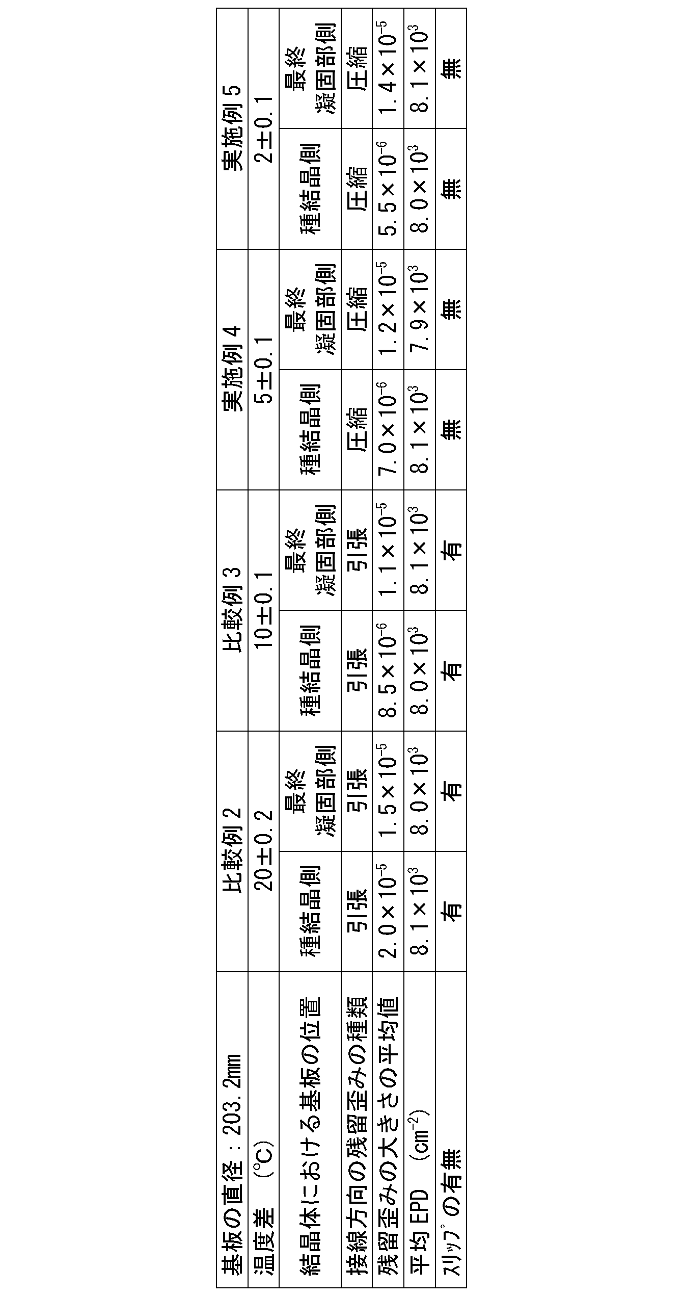
- (Comparative Example 2) Production of GaAs Single Crystal Using a production apparatus shown in FIG. 2, a C (carbon) -doped semi-insulating GaAs single crystal having a straight body portion having a diameter of 208 mm and a length of 100 mm is produced by the VB method. . GaAs polycrystal is used as a GaAs raw material. B 2 O 3 is used as a sealing material. A GaAs single crystal is grown by adjusting the temperature distribution in the manufacturing apparatus so that the temperature gradient in the crystal growth direction at the crystal growth interface is 2 ° C./cm. Next, the grown GaAs single crystal is cooled to room temperature (25 ° C.) at a rate of 25 ° C./min.
- the temperature difference in the GaAs single crystal body is 20 ⁇ 0.2 ° C. in the entire straight body of the GaAs single crystal body.
- GaAs Single Crystal Substrate The GaAs single crystal obtained above was sliced along a plane perpendicular to the central axis of the straight body portion, and both front and back main surfaces were subjected to mechanical polishing and chemical mechanical polishing (CMP). By mirror finishing, two GaAs single crystal substrates having a diameter of 203.2 mm and a thickness of 700 ⁇ m (one each from the seed crystal side and the final solidification part side) are produced. There is no work-affected layer on both main surfaces on the front and back after polishing. Note that various cleanings that can maintain the mirror surface after polishing may be performed.
- CMP chemical mechanical polishing
- the type (compression or tension) of the residual strain in the tangential direction in the outer peripheral portion was measured by Raman spectrum using a Raman spectrophotometer (HR evolution manufactured by HORIBA), and Raman shift was performed. To evaluate from. The determination of the direction of the residual strain in the tangential direction does not specify the magnitude, so that a measurement method other than Raman shift may be used as long as the direction can be determined. Evaluation of the average value of the magnitude of the residual strain expressed by the absolute value
- the light irradiation diameter on the main surface of the substrate is ⁇ 100 ⁇ m.
- the average value of the magnitude of the residual strain in the outer peripheral portion was measured by scanning the entire main surface at 0.5 mm pitch square lattice points so that the center of the main surface of the substrate was included in the measurement location, and measured from the outer periphery to the center. An average value is calculated from all the measurement values included in the outer peripheral portion from the inner periphery of 10 mm toward the outside and 5 mm inward from the outer periphery toward.
- the crystallinity is evaluated by an average EPD (etching pit density) in the entire area 5 mm inside from the outer peripheral surface.
- molten potassium hydroxide is used as an etching solution.
- the EPD can be obtained by magnifying the main surface of the GaAs single crystal substrate by 100 times with a microscope and counting the number of etch pits within a 1 mm square visual field.
- the average value of the EPD can be obtained by counting the number of etch pits at 5 mm intervals along each direction in four equivalent ⁇ 110> directions from the center of the main surface, and calculating the average value of these numbers. Further, even in the four equivalent ⁇ 100> directions from the center of the main surface, the number of etch pits can be counted at intervals of 5 mm along each direction, thereby obtaining an average value of these numbers.
- the presence or absence of slip is evaluated by applying the same thermal history as in the case of growing the semiconductor layer on the GaAs single crystal substrate. Specifically, the GaAs single crystal substrate is heated to 600 ° C. at a rate of 40 ° C./min and maintained for 10 minutes under an AsH 3 (arsine) atmosphere in an OMVPE (metal organic chemical vapor deposition) furnace. After cooling at a rate of 100 ° C./min, the occurrence of slip on the GaAs single crystal substrate is observed with a differential interference microscope. The results are summarized in Table 2.
- GaAs single crystal having a diameter of a straight body of 208 mm and a length of 100 mm is produced by a VB method using the production apparatus shown in FIG.
- GaAs polycrystal is used as a GaAs raw material.
- B 2 O 3 is used as a sealing material.
- a high-purity high-alumina fiber heat insulating material (Denka Arsen, manufactured by Denka Corporation) having a thickness of 5 mm is used as a heat insulating material.
- a GaAs single crystal is grown by adjusting the temperature distribution in the manufacturing apparatus so that the temperature gradient in the crystal growth direction at the crystal growth interface is 2 ° C./cm.
- the grown GaAs single crystal is cooled to a soaking temperature of 1100 ° C., kept for 10 hours, and then cooled at a rate of 25 ° C./min.
- the temperature distribution of the heater is adjusted so that the temperature difference in the GaAs single crystal measured by the same method as in Comparative Example 2 becomes 10 ⁇ 0.1 ° C.
- a GaAs single crystal having a straight body portion with a diameter of 203.2 mm is produced in the same manner as in Comparative Example 2.
- GaAs single crystal substrates having a diameter of 203.2 mm and a thickness of 700 ⁇ m are produced from the GaAs single crystal obtained above in the same manner as in Comparative Example 2.
- the type of residual strain in the tangential direction (compression or tension) in the outer peripheral portion and the average value of the magnitude of the residual strain in the outer peripheral portion are evaluated. The results are summarized in Table 2.
- Example 4 Production of GaAs Single Crystal
- GaAs polycrystal is used as a GaAs raw material.
- B 2 O 3 is used as a sealing material.
- a high-purity high-alumina fiber heat insulating material (Denka Arsen, manufactured by Denka Corporation) having a thickness of 5 mm is used as a heat insulating material.
- a GaAs single crystal is grown by adjusting the temperature distribution in the manufacturing apparatus so that the temperature gradient in the crystal growth direction at the crystal growth interface is 2 ° C./cm.
- the grown GaAs single crystal is cooled to a soaking temperature of 1100 ° C., kept for 10 hours, and then cooled at a rate of 25 ° C./min.
- the temperature distribution of the heater is adjusted so that the temperature difference in the GaAs single crystal measured by the same method as in Comparative Example 2 becomes 5 ⁇ 0.1 ° C.
- a GaAs single crystal having a straight body portion with a diameter of 203.2 mm is produced in the same manner as in Comparative Example 2.
- GaAs single crystal substrates having a diameter of 203.2 mm and a thickness of 700 ⁇ m are produced from the GaAs single crystal obtained above in the same manner as in Comparative Example 2.
- the type of residual strain in the tangential direction (compression or tension) in the outer peripheral portion and the average value of the magnitude of the residual strain in the outer peripheral portion are evaluated. The results are summarized in Table 2.
- Example 5 Production of GaAs Single Crystal
- GaAs polycrystal is used as a GaAs raw material.
- B 2 O 3 is used as a sealing material.
- a high-purity high-alumina fiber heat insulating material (Denka Arsen, manufactured by Denka Corporation) having a thickness of 5 mm is used as a heat insulating material.
- a GaAs single crystal is grown by adjusting the temperature distribution in the manufacturing apparatus so that the temperature gradient in the crystal growth direction at the crystal growth interface is 2 ° C./cm.
- the grown GaAs single crystal is cooled to a soaking temperature of 1100 ° C., kept for 10 hours, and then cooled at a rate of 25 ° C./min.
- the temperature distribution of the heater is adjusted so that the temperature difference in the GaAs single crystal measured by the same method as in Comparative Example 2 is 2 ⁇ 0.1 ° C.
- a GaAs single crystal having a straight body portion with a diameter of 203.2 mm is produced in the same manner as in Comparative Example 2.
- GaAs single crystal substrates having a diameter of 203.2 mm and a thickness of 700 ⁇ m are produced from the GaAs single crystal obtained above in the same manner as in Comparative Example 2.
- the type of residual strain in the tangential direction (compression or tension) in the outer peripheral portion and the average value of the magnitude of the residual strain in the outer peripheral portion are evaluated. The results are summarized in Table 2.
- the GaAs single crystal and the GaAs single crystal substrate whose tangential residual strain in the outer peripheral portion is a compressive strain are obtained.
- no slip occurs on the GaAs single crystal substrate.
- 1 ⁇ GaAs single crystal substrate 1c, 10c inner peripheral portion, 1d, 10d outer peripheral portion, 1e outer peripheral, 1i inner peripheral, 1o central, 10 ⁇ GaAs single crystal body, 10e outer peripheral surface, 10i inner peripheral surface, 10o central axis, 11 GaAs Seed crystal, 13% GaAs raw material, 20% production equipment, 21 ° container, 21 ° container body, 21p container lid, 22 ° crucible, 23 ° sealing material, 24 ° heat insulating material, 25 ° holding stand, 26 ° heater.
Landscapes
- Chemical & Material Sciences (AREA)
- Engineering & Computer Science (AREA)
- Crystallography & Structural Chemistry (AREA)
- Materials Engineering (AREA)
- Metallurgy (AREA)
- Organic Chemistry (AREA)
- Inorganic Chemistry (AREA)
- Crystals, And After-Treatments Of Crystals (AREA)
Abstract
Description
特開平11-268997号公報(特許文献1)に開示のGaAs結晶または特開2012-236750号公報(特許文献2)に開示のGaAs単結晶ウエハは、その上に半導体層を成長させる際の成長温度までの昇温速度が速い場合に、GaAs結晶またはGaAs単結晶ウエハにスリップが発生するという問題点があった。ここで、スリップとは、転位が容易すべり系を限定的に運動する際にみられるもので、表面が鏡面研磨された単結晶ウエハで発生した場合は、GaAs単結晶ウエハ表面の段差として、微分干渉顕微鏡で観察され、著しい場合は目視でも観察される。スリップ部は、転位が高密度に存在することから、後工程でデバイス等の不良につながる。このため、スリップの発生を防止する必要がある。かかるスリップは、GaAs結晶成長中の熱応力あるいはGaAs単結晶ウエハを使用する際の応力によって発生するものと考えられる。
[本開示の効果]
本開示によれば、その上に半導体層を成長させる際にスリップの発生が抑制されるヒ化ガリウム単結晶体およびヒ化ガリウム単結晶基板を提供できる。
最初に本開示の実施態様を列記して説明する。
<実施形態1:ヒ化ガリウム単結晶体>
(ヒ化ガリウム単結晶体)
図1を参照して、本実施形態のGaAs単結晶体10(ヒ化ガリウム単結晶体)は、円柱状の直胴部を含み、直胴部の外周面10eから中心軸10oに向かって10mmの内周面10iから外側でかつ外周面10eから5mm内側までの外周部10dにおける接線方向TDの残留歪みが圧縮歪みである。ここで、GaAs単結晶体10の外周部10dにおける残留歪みとは、GaAs単結晶体10の外周部10dにおいて任意に特定される点Pにおける残留歪みをいう。残留歪みの方向は、半径方向RDと接線方向TDとに分けられる。半径方向RDとは、中心軸10oと任意に特定される点Pとを結ぶ半径の方向である。接線方向TDとは、その点Pにおける半径方向に垂直な方向であり、周方向とも呼ばれる。残留歪みの種類には、圧縮歪みと引張歪みとがある。
図2に典型的なGaAs(ヒ化ガリウム)単結晶体の製造装置および製造方法を示し、図3に本実施形態のGaAs(ヒ化ガリウム)単結晶体の製造装置および製造方法を示す。
図2および図3を参照して、典型的なGaAs単結晶体および本実施形態のGaAs単結晶体10の製造方法は、結晶品質が高く、製品であるGaAs単結晶基板となる直胴部が長いGaAs単結晶体10を得る観点から、上記の製造装置20を用いて、VB(垂直ボート)法などのボート法によることが好ましい。具体的には、本実施形態のGaAs単結晶体10の製造方法は、好ましくは、GaAs種結晶装入工程、GaAs原料装入工程、封止材配置工程、結晶成長工程、および冷却工程を含む。
(ヒ化ガリウム単結晶基板)
図6を参照して、本実施形態のGaAs単結晶基板1(ヒ化ガリウム単結晶基板)は、外周1eから中心1oに向かって10mmの内周1iから外側でかつ外周1eから5mm内側までの外周部1dにおける接線方向TDの残留歪みが圧縮歪みである。ここで、GaAs単結晶基板1の外周部1dにおける残留歪みとは、GaAs単結晶基板1の外周部1dにおいて任意に特定される点Pにおける残留歪みをいう。残留歪みの方向は、半径方向RDと接線方向TDとに分けられる。半径方向RDとは、中心軸10oと任意に特定される点Pとを結ぶ半径の方向である。接線方向TDとは、その点Pにおける半径方向に垂直な方向であり、周方向とも呼ばれる。残留歪みの種類には、圧縮歪みと引張歪みとがある。
GaAs単結晶基板1の製造方法は、特に制限はなく、たとえば、実施形態1のGaAs単結晶体10をその中心軸10oに垂直な面で切り出し、主面を鏡面加工する方法が好適に挙げられる。
1.GaAs単結晶体の作製
図2に示す製造装置を用いて、VB法により直胴部の直径が156mmで長さが200mmのC(炭素)をドープした半絶縁性のGaAs単結晶体を作製する。GaAs原料としてGaAs多結晶を用いる。封止材としてB2O3を用いる。結晶成長界面の結晶成長方向の温度勾配が2℃/cmとなるように製造装置内の温度分布を調整して、GaAs単結晶体を成長させる。次に、成長させたGaAs単結晶体を25℃/分で室温(25℃)まで冷却する。このときのGaAs単結晶体中の温度差は、GaAs単結晶体の直胴部全体で、20±0.2℃である。冷却後のGaAs単結晶体から、その外周面を研削することにより、直胴部の直径が152.4mmのGaAs単結晶体を作製する。
上記で得られたGaAs単結晶体から、その直胴部の中心軸に垂直な面でスライスして表裏の両主面を機械的研磨および化学機械的研磨(CMP)により鏡面仕上げをして、直径が152.4mmで厚さが700μmのGaAs単結晶基板を2枚(種結晶側および最終凝固部側からそれぞれ1枚)作製する。研磨後の表裏の両主面には加工変質層は存在しない。なお、研磨後に鏡面を維持できる各種洗浄を施してもよい。このようにして得られたGaAs単結晶基板について、外周部における接線方向の残留歪みの種類(圧縮または引張)をラマン分光光度計(HORIBA社製HR evolution)を用いてラマンスペクトルを測定しラマンシフトから評価する。なお、接線方向の残留歪の向きの判定は、大きさを特定するのではないので、向きを判別できるならばラマンシフト以外の測定方法を用いてもよい。半径方向の歪み成分Srと接線方向の歪み成分Stとの差の絶対値|Sr-St|で表される残留歪みの大きさの外周部における平均値の評価を、たとえば、Appl.Phys.Lett.47(1985)pp.365-367に記載されている光弾性法に基づいて行うことができる。具体的には、基板主面上での光照射径はφ100μmである。上記残留歪みの大きさの外周部における平均値は、基板主面の中心が測定箇所に含まれるように主面の全面を0.5mmピッチの正方格子点でスキャンした測定を行い、外周から中心に向かって10mmの内周から外側でかつ外周から5mm内側までの外周部に含まれる全測定値から平均値を算出する。結晶性は、外周面から5mm内側全体における平均EPD(エッチングピット密度)で評価する。具体的には、エッチング液として溶融水酸化カリウムを用いる。EPDは、GaAs単結晶基板の主面を顕微鏡により100倍に拡大し、その1mm角(1mm×1mmの正方形を意味する、以下同じ)視野内のエッチピット数をカウントすることにより求めることができる。EPDの平均値は、主面の中心から<110>方向の等価な4方向に対し、各方向に沿って5mm間隔でエッチピット数をカウントし、これらの数の平均値として求めることができる。さらに主面の中心から<100>方向の等価な4方向に対しても、各方向に沿って5mm間隔でエッチピット数をカウントすることにより、これらの数の平均値として求めることができる。
上記のGaAs単結晶基板上に半導体層を成長させる場合と同様の熱履歴を加えることにより、スリップの発生の有無を評価する。具体的には、上記のGaAs単結晶基板を、OMVPE(有機金属気相成長)炉内におけるAsH3(アルシン)雰囲気下で、600℃まで40℃/分の速度で昇温し、10分間保持し、100℃/分の設定で冷却した後、GaAs単結晶基板におけるスリップ発生の有無を微分干渉顕微鏡により観察する。結果を表1にまとめる。
1.GaAs単結晶体の作製
図3に示す製造装置を用いて、比較例1と同様にVB法により直胴部の直径が156mmで長さが200mmの半絶縁性のGaAs単結晶体を作製する。GaAs原料としてGaAs多結晶を用いる。封止材としてB2O3を用いる。保温材として厚さ5mmの高純度高アルミナ繊維断熱材(デンカ社製デンカアルセン)を用いる。結晶成長界面の結晶成長方向の温度勾配が2℃/cmとなるように製造装置内の温度分布を調整して、GaAs単結晶体を成長させる。次に、成長させたGaAs単結晶体を均熱化温度1100℃まで冷却し、10時間保持した後25℃/分で冷却する。このときの比較例1と同様の方法で測定されるGaAs単結晶体中の温度差が10±0.1℃になるようにヒータの温度分布を調節する。冷却後のGaAs単結晶体から、比較例1と同様にして、直胴部の直径が152.4mmのGaAs単結晶体を作製する。
上記で得られたGaAs単結晶体から、比較例1と同様にして、直径が152.4mmで厚さが700μmのGaAs単結晶基板を2枚作製する。得られたGaAs単結晶基板について、比較例1と同様にして、外周部における接線方向の残留歪みの種類(圧縮または引張」)および残留歪みの大きさの外周部における平均値を評価する。結果を表1にまとめる。
上記のGaAs単結晶基板について、比較例1と同様にして、GaAs単結晶基板におけるスリップ発生の有無を評価する。結果を表1にまとめる。
1.GaAs単結晶体の作製
図3に示す製造装置を用いて、比較例1と同様にVB法により直胴部の直径が156mmで長さが200mmの半絶縁性のGaAs単結晶体を作製する。GaAs原料としてGaAs多結晶を用いる。封止材としてB2O3を用いる。保温材として厚さ5mmの高純度高アルミナ繊維断熱材(デンカ社製デンカアルセン)を用いる。結晶成長界面の結晶成長方向の温度勾配が2℃/cmとなるように製造装置内の温度分布を調整して、GaAs単結晶体を成長させる。次に、成長させたGaAs単結晶体を均熱化温度1100℃まで冷却し、10時間保持した後25℃/分で冷却する。このときの比較例1と同様の方法で測定されるGaAs単結晶体中の温度差が5±0.1℃になるようにヒータの温度分布を調節する。冷却後のGaAs単結晶体から、比較例1と同様にして、直胴部の直径が152.4mmのGaAs単結晶体を作製する。
上記で得られたGaAs単結晶体から、比較例1と同様にして、直径が152.4mmで厚さが700μmのGaAs単結晶基板を2枚作製する。得られたGaAs単結晶基板について、比較例1と同様にして、外周部における接線方向の残留歪みの種類(圧縮または引張」)および残留歪みの大きさの外周部における平均値を評価する。結果を表1にまとめる。
上記のGaAs単結晶基板について、比較例1と同様にして、GaAs単結晶基板におけるスリップ発生の有無を評価する。結果を表1にまとめる。
1.GaAs単結晶体の作製
図3に示す製造装置を用いて、比較例1と同様にVB法により直胴部の直径が156mmで長さが200mmの半絶縁性のGaAs単結晶体を作製する。GaAs原料としてGaAs多結晶を用いる。封止材としてB2O3を用いる。保温材として厚さ5mmの高純度高アルミナ繊維断熱材(デンカ社製デンカアルセン)を用いる。結晶成長界面の結晶成長方向の温度勾配が2℃/cmとなるように製造装置内の温度分布を調整して、GaAs単結晶体を成長させる。次に、成長させたGaAs単結晶体を均熱化温度1100℃まで冷却し、10時間保持した後25℃/分で冷却する。このときの比較例1と同様の方法で測定されるGaAs単結晶体中の温度差が2±0.1℃になるようにヒータの温度分布を調節する。冷却後のGaAs単結晶体から、比較例1と同様にして、直胴部の直径が152.4mmのGaAs単結晶体を作製する。
上記で得られたGaAs単結晶体から、比較例1と同様にして、直径が152.4mmで厚さが700μmのGaAs単結晶基板を2枚作製する。得られたGaAs単結晶基板について、比較例1と同様にして、外周部における接線方向の残留歪みの種類(圧縮または引張)および残留歪みの大きさの外周部における平均値を評価する。結果を表1にまとめる。
上記のGaAs単結晶基板について、比較例1と同様にして、GaAs単結晶基板におけるスリップ発生の有無を評価する。結果を表1にまとめる。

1.GaAs単結晶体の作製
図2に示す製造装置を用いて、VB法により直胴部の直径が208mmで長さが100mmのC(炭素)をドープした半絶縁性のGaAs単結晶体を作製する。GaAs原料としてGaAs多結晶を用いる。封止材としてB2O3を用いる。結晶成長界面の結晶成長方向の温度勾配が2℃/cmとなるように製造装置内の温度分布を調整して、GaAs単結晶体を成長させる。次に、成長させたGaAs単結晶体を25℃/分で室温(25℃)まで冷却する。このときのGaAs単結晶体中の温度差は、GaAs単結晶体の直胴部全体で、20±0.2℃である。冷却後のGaAs単結晶体から、その外周面を研削することにより、直胴部の直径が203.2mmのGaAs単結晶体を作製する。
上記で得られたGaAs単結晶体から、その直胴部の中心軸に垂直な面でスライスして表裏の両主面を機械的研磨および化学機械的研磨(CMP)により鏡面仕上げをして、直径が203.2mmで厚さが700μmのGaAs単結晶基板を2枚(種結晶側および最終凝固部側からそれぞれ1枚)作製する。研磨後の表裏の両主面には加工変質層は存在しない。なお、研磨後に鏡面を維持できる各種洗浄を施してもよい。このようにして得られたGaAs単結晶基板について、外周部における接線方向の残留歪みの種類(圧縮または引張)をラマン分光光度計(HORIBA社製HR evolution)を用いてラマンスペクトルを測定しラマンシフトから評価する。なお、接線方向の残留歪の向きの判定は、大きさを特定するのではないので、向きを判別できるならばラマンシフト以外の測定方法を用いてもよい。半径方向の歪み成分Srと接線方向の歪み成分Stとの差の絶対値|Sr-St|で表される残留歪みの大きさの外周部における平均値の評価を、たとえば、Appl.Phys.Lett.47(1985)pp.365-367に記載されている光弾性法に基づいて行うことができる。具体的には、基板主面上での光照射径はφ100μmである。上記残留歪みの大きさの外周部における平均値は、基板主面の中心が測定箇所に含まれるように主面の全面を0.5mmピッチの正方格子点でスキャンした測定を行い、外周から中心に向かって10mmの内周から外側でかつ外周から5mm内側までの外周部に含まれる全測定値から平均値を算出する。結晶性は、外周面から5mm内側全体における平均EPD(エッチングピット密度)で評価する。具体的には、エッチング液として溶融水酸化カリウムを用いる。EPDは、GaAs単結晶基板の主面を顕微鏡により100倍に拡大し、その1mm角視野内のエッチピット数をカウントすることにより求めることができる。EPDの平均値は、主面の中心から<110>方向の等価な4方向に対し、各方向に沿って5mm間隔でエッチピット数をカウントし、これらの数の平均値として求めることができる。さらに主面の中心から<100>方向の等価な4方向に対しても、各方向に沿って5mm間隔でエッチピット数をカウントすることにより、これらの数の平均値として求めることができる。
上記のGaAs単結晶基板上に半導体層を成長させる場合と同様の熱履歴を加えることにより、スリップの発生の有無を評価する。具体的には、上記のGaAs単結晶基板を、OMVPE(有機金属気相成長)炉内におけるAsH3(アルシン)雰囲気下で、600℃まで40℃/分の速度で昇温し、10分間保持し、100℃/分の設定で冷却した後、GaAs単結晶基板におけるスリップ発生の有無を微分干渉顕微鏡により観察する。結果を表2にまとめる。
1.GaAs単結晶体の作製
図3に示す製造装置を用いて、比較例2と同様にVB法により直胴部の直径が208mmで長さが100mmの半絶縁性のGaAs単結晶体を作製する。GaAs原料としてGaAs多結晶を用いる。封止材としてB2O3を用いる。保温材として厚さ5mmの高純度高アルミナ繊維断熱材(デンカ社製デンカアルセン)を用いる。結晶成長界面の結晶成長方向の温度勾配が2℃/cmとなるように製造装置内の温度分布を調整して、GaAs単結晶体を成長させる。次に、成長させたGaAs単結晶体を均熱化温度1100℃まで冷却し、10時間保持した後25℃/分で冷却する。このときの比較例2と同様の方法で測定されるGaAs単結晶体中の温度差が10±0.1℃になるようにヒータの温度分布を調節する。冷却後のGaAs単結晶体から、比較例2と同様にして、直胴部の直径が203.2mmのGaAs単結晶体を作製する。
上記で得られたGaAs単結晶体から、比較例2と同様にして、直径が203.2mmで厚さが700μmのGaAs単結晶基板を2枚作製する。得られたGaAs単結晶基板について、比較例2と同様にして、外周部における接線方向の残留歪みの種類(圧縮または引張」)および残留歪みの大きさの外周部における平均値を評価する。結果を表2にまとめる。
上記のGaAs単結晶基板について、比較例2と同様にして、GaAs単結晶基板におけるスリップ発生の有無を評価する。結果を表2にまとめる。
1.GaAs単結晶体の作製
図3に示す製造装置を用いて、比較例2と同様にVB法により直胴部の直径が208mmで長さが100mmの半絶縁性のGaAs単結晶体を作製する。GaAs原料としてGaAs多結晶を用いる。封止材としてB2O3を用いる。保温材として厚さ5mmの高純度高アルミナ繊維断熱材(デンカ社製デンカアルセン)を用いる。結晶成長界面の結晶成長方向の温度勾配が2℃/cmとなるように製造装置内の温度分布を調整して、GaAs単結晶体を成長させる。次に、成長させたGaAs単結晶体を均熱化温度1100℃まで冷却し、10時間保持した後25℃/分で冷却する。このときの比較例2と同様の方法で測定されるGaAs単結晶体中の温度差が5±0.1℃になるようにヒータの温度分布を調節する。冷却後のGaAs単結晶体から、比較例2と同様にして、直胴部の直径が203.2mmのGaAs単結晶体を作製する。
上記で得られたGaAs単結晶体から、比較例2と同様にして、直径が203.2mmで厚さが700μmのGaAs単結晶基板を2枚作製する。得られたGaAs単結晶基板について、比較例2と同様にして、外周部における接線方向の残留歪みの種類(圧縮または引張」)および残留歪みの大きさの外周部における平均値を評価する。結果を表2にまとめる。
上記のGaAs単結晶基板について、比較例2と同様にして、GaAs単結晶基板におけるスリップ発生の有無を評価する。結果を表2にまとめる。
1.GaAs単結晶体の作製
図3に示す製造装置を用いて、比較例2と同様にVB法により直胴部の直径が208mmで長さが100mmの半絶縁性のGaAs単結晶体を作製する。GaAs原料としてGaAs多結晶を用いる。封止材としてB2O3を用いる。保温材として厚さ5mmの高純度高アルミナ繊維断熱材(デンカ社製デンカアルセン)を用いる。結晶成長界面の結晶成長方向の温度勾配が2℃/cmとなるように製造装置内の温度分布を調整して、GaAs単結晶体を成長させる。次に、成長させたGaAs単結晶体を均熱化温度1100℃まで冷却し、10時間保持した後25℃/分で冷却する。このときの比較例2と同様の方法で測定されるGaAs単結晶体中の温度差が2±0.1℃になるようにヒータの温度分布を調節する。冷却後のGaAs単結晶体から、比較例2と同様にして、直胴部の直径が203.2mmのGaAs単結晶体を作製する。
上記で得られたGaAs単結晶体から、比較例2と同様にして、直径が203.2mmで厚さが700μmのGaAs単結晶基板を2枚作製する。得られたGaAs単結晶基板について、比較例1と同様にして、外周部における接線方向の残留歪みの種類(圧縮または引張)および残留歪みの大きさの外周部における平均値を評価する。結果を表2にまとめる。
上記のGaAs単結晶基板について、比較例2と同様にして、GaAs単結晶基板におけるスリップ発生の有無を評価する。結果を表2にまとめる。
Claims (6)
- 円柱状の直胴部を含み、
前記直胴部の外周面から中心軸に向かって10mmの内周面から外側でかつ前記外周面から5mm内側までの外周部における接線方向の残留歪みが圧縮歪みであるヒ化ガリウム単結晶体。 - 半径方向の歪み成分Srと接線方向の歪み成分Stとの差の絶対値|Sr-St|で表される残留歪みの大きさの前記外周部における平均値が2.5×10⁻⁶以上1.5×10⁻⁵以下である請求項1に記載のヒ化ガリウム単結晶体。
- 前記直胴部の直径が100mm以上305mm以下である請求項1または請求項2に記載のヒ化ガリウム単結晶体。
- 外周から中心に向かって10mmの内周から外側でかつ前記外周から5mm内側までの外周部における接線方向の残留歪みが圧縮歪みであるヒ化ガリウム単結晶基板。
- 半径方向の歪み成分Srと接線方向の歪み成分Stとの差の絶対値|Sr-St|で表される残留歪みの大きさの前記外周部における平均値が2.5×10⁻⁶以上1.5×10⁻⁵以下である請求項4に記載のヒ化ガリウム単結晶基板。
- 直径が100mm以上305mm以下である請求項4または請求項5に記載のヒ化ガリウム単結晶基板。
Priority Applications (7)
| Application Number | Priority Date | Filing Date | Title |
|---|---|---|---|
| CN201880091881.9A CN111902573B (zh) | 2018-08-07 | 2018-08-07 | 砷化镓单晶和砷化镓单晶基板 |
| EP18929084.4A EP3835465A4 (en) | 2018-08-07 | 2018-08-07 | GALLIUM ARSENIDE SINGLE CRYSTAL, AND GALLIUM ARSENIDE SINGLE CRYSTAL SUBSTRATE |
| JP2019527486A JP6737405B2 (ja) | 2018-08-07 | 2018-08-07 | ヒ化ガリウム単結晶体およびヒ化ガリウム単結晶基板 |
| US16/963,682 US12338546B2 (en) | 2018-08-07 | 2018-08-07 | Gallium arsenide single crystal and gallium arsenide single crystal substrate |
| PCT/JP2018/029679 WO2020031273A1 (ja) | 2018-08-07 | 2018-08-07 | ヒ化ガリウム単結晶体およびヒ化ガリウム単結晶基板 |
| TW108105266A TWI817985B (zh) | 2018-08-07 | 2019-02-18 | 砷化鎵單晶體及砷化鎵單晶基板 |
| TW112137674A TW202405266A (zh) | 2018-08-07 | 2019-02-18 | 砷化鎵單晶體及砷化鎵單晶基板 |
Applications Claiming Priority (1)
| Application Number | Priority Date | Filing Date | Title |
|---|---|---|---|
| PCT/JP2018/029679 WO2020031273A1 (ja) | 2018-08-07 | 2018-08-07 | ヒ化ガリウム単結晶体およびヒ化ガリウム単結晶基板 |
Publications (1)
| Publication Number | Publication Date |
|---|---|
| WO2020031273A1 true WO2020031273A1 (ja) | 2020-02-13 |
Family
ID=69413251
Family Applications (1)
| Application Number | Title | Priority Date | Filing Date |
|---|---|---|---|
| PCT/JP2018/029679 Ceased WO2020031273A1 (ja) | 2018-08-07 | 2018-08-07 | ヒ化ガリウム単結晶体およびヒ化ガリウム単結晶基板 |
Country Status (6)
| Country | Link |
|---|---|
| US (1) | US12338546B2 (ja) |
| EP (1) | EP3835465A4 (ja) |
| JP (1) | JP6737405B2 (ja) |
| CN (1) | CN111902573B (ja) |
| TW (2) | TWI817985B (ja) |
| WO (1) | WO2020031273A1 (ja) |
Families Citing this family (1)
| Publication number | Priority date | Publication date | Assignee | Title |
|---|---|---|---|---|
| DE102023200457A1 (de) | 2023-01-20 | 2024-07-25 | Freiberger Compound Materials Gesellschaft mit beschränkter Haftung | Vorrichtung und Verfahren zur Herstellung von AIII-BV-Verbindungshalbleiter-Einkristallen sowie AIII-BV-Verbindungshalbleiter-Einkristall und -Wafer |
Citations (4)
| Publication number | Priority date | Publication date | Assignee | Title |
|---|---|---|---|---|
| JPS59182298A (ja) * | 1983-03-30 | 1984-10-17 | Toshiba Corp | 化合物半導体単結晶の製造方法 |
| JPH09321105A (ja) * | 1996-03-25 | 1997-12-12 | Sumitomo Electric Ind Ltd | 半導体ウエハの評価方法、熱処理方法、および熱処理装置 |
| JPH11268997A (ja) | 1998-03-24 | 1999-10-05 | Sumitomo Electric Ind Ltd | GaAs単結晶の熱処理方法およびGaAs基板 |
| JP2012236750A (ja) | 2011-05-13 | 2012-12-06 | Hitachi Cable Ltd | GaAs単結晶ウエハ及びその製造方法 |
Family Cites Families (11)
| Publication number | Priority date | Publication date | Assignee | Title |
|---|---|---|---|---|
| JP3656261B2 (ja) * | 1994-10-24 | 2005-06-08 | 住友電気工業株式会社 | GaAs結晶の熱処理方法 |
| US6045767A (en) * | 1997-11-21 | 2000-04-04 | American Xtal Technology | Charge for vertical boat growth process and use thereof |
| JP2967780B1 (ja) * | 1998-09-28 | 1999-10-25 | 住友電気工業株式会社 | GaAs単結晶基板およびそれを用いたエピタキシャルウェハ |
| JP4144349B2 (ja) | 2002-12-26 | 2008-09-03 | 日立電線株式会社 | 化合物半導体製造装置 |
| JP3818311B1 (ja) * | 2005-03-23 | 2006-09-06 | 住友電気工業株式会社 | 結晶育成用坩堝 |
| JP4655861B2 (ja) | 2005-10-07 | 2011-03-23 | 日立電線株式会社 | 電子デバイス用基板の製造方法 |
| JP2012031004A (ja) * | 2010-07-30 | 2012-02-16 | Hitachi Cable Ltd | 半絶縁性GaAs単結晶ウエハ |
| CN107039516B (zh) * | 2011-05-18 | 2020-07-10 | 住友电气工业株式会社 | 化合物半导体衬底 |
| JP2013170103A (ja) * | 2012-02-21 | 2013-09-02 | Hitachi Cable Ltd | 半絶縁性砒化ガリウムウェハの製造方法及び半絶縁性砒化ガリウムウェハ |
| JP2013193917A (ja) * | 2012-03-19 | 2013-09-30 | Hitachi Cable Ltd | 半絶縁性砒化ガリウムウェハの製造方法及び半絶縁性砒化ガリウムウェハ |
| JP7783786B2 (ja) * | 2022-06-14 | 2025-12-10 | 鹿島建設株式会社 | 鉄筋籠の建て込み方法 |
-
2018
- 2018-08-07 CN CN201880091881.9A patent/CN111902573B/zh active Active
- 2018-08-07 WO PCT/JP2018/029679 patent/WO2020031273A1/ja not_active Ceased
- 2018-08-07 US US16/963,682 patent/US12338546B2/en active Active
- 2018-08-07 JP JP2019527486A patent/JP6737405B2/ja active Active
- 2018-08-07 EP EP18929084.4A patent/EP3835465A4/en active Pending
-
2019
- 2019-02-18 TW TW108105266A patent/TWI817985B/zh active
- 2019-02-18 TW TW112137674A patent/TW202405266A/zh unknown
Patent Citations (4)
| Publication number | Priority date | Publication date | Assignee | Title |
|---|---|---|---|---|
| JPS59182298A (ja) * | 1983-03-30 | 1984-10-17 | Toshiba Corp | 化合物半導体単結晶の製造方法 |
| JPH09321105A (ja) * | 1996-03-25 | 1997-12-12 | Sumitomo Electric Ind Ltd | 半導体ウエハの評価方法、熱処理方法、および熱処理装置 |
| JPH11268997A (ja) | 1998-03-24 | 1999-10-05 | Sumitomo Electric Ind Ltd | GaAs単結晶の熱処理方法およびGaAs基板 |
| JP2012236750A (ja) | 2011-05-13 | 2012-12-06 | Hitachi Cable Ltd | GaAs単結晶ウエハ及びその製造方法 |
Non-Patent Citations (2)
| Title |
|---|
| APPL. PHYS. LETT., vol. 47, 1985, pages 365 - 367 |
| See also references of EP3835465A4 |
Also Published As
| Publication number | Publication date |
|---|---|
| CN111902573A (zh) | 2020-11-06 |
| TWI817985B (zh) | 2023-10-11 |
| EP3835465A4 (en) | 2022-03-16 |
| EP3835465A1 (en) | 2021-06-16 |
| TW202405266A (zh) | 2024-02-01 |
| US12338546B2 (en) | 2025-06-24 |
| TW202007800A (zh) | 2020-02-16 |
| JPWO2020031273A1 (ja) | 2020-08-20 |
| CN111902573B (zh) | 2024-03-08 |
| US20210079556A1 (en) | 2021-03-18 |
| JP6737405B2 (ja) | 2020-08-05 |
Similar Documents
| Publication | Publication Date | Title |
|---|---|---|
| CN102449208B (zh) | SiC单晶的制造方法 | |
| JP7085833B2 (ja) | 炭化珪素単結晶の製造方法 | |
| JP3156382B2 (ja) | 化合物半導体単結晶およびその成長方法 | |
| JP7161784B2 (ja) | 炭化珪素インゴット、ウエハ及びその製造方法 | |
| KR101313462B1 (ko) | 실리콘 웨이퍼의 열처리 방법 | |
| JP4585359B2 (ja) | 炭化珪素単結晶の製造方法 | |
| WO2020116458A1 (ja) | 単結晶育成用ルツボ、単結晶製造方法及び単結晶 | |
| JP6645409B2 (ja) | シリコン単結晶製造方法 | |
| JP6737405B2 (ja) | ヒ化ガリウム単結晶体およびヒ化ガリウム単結晶基板 | |
| TWI806990B (zh) | 磷化銦單晶體及磷化銦單晶基板 | |
| CN106245000B (zh) | 热分解氮化硼容器的制造方法及热分解氮化硼容器 | |
| JP5545265B2 (ja) | GaAs単結晶ウエハ及びGaAs単結晶の製造方法 | |
| JP5948988B2 (ja) | 炭化珪素単結晶の製造方法 | |
| JP2011251892A (ja) | InP単結晶およびその製造方法 | |
| US20250361646A1 (en) | Single crystal silicon ingot and method of growing the same | |
| KR101966707B1 (ko) | 종자결정의 소형화 또는 박형화를 가능하게 하고 내부 결함 발생을 억제하는 종자결정의 지지구조 및 이로부터 제조되는 단결정 | |
| Tsuge et al. | Growth of high quality 4H-SiC crystals in controlled temperature distributions of seed crystals | |
| JP2008273804A (ja) | 半絶縁性GaAsウエハ及びその製造方法 | |
| JP2013193917A (ja) | 半絶縁性砒化ガリウムウェハの製造方法及び半絶縁性砒化ガリウムウェハ | |
| KR20180024458A (ko) | 실리콘카바이드 단결정의 제조 장치 및 실리콘카바이드 단결정의 제조 방법 |
Legal Events
| Date | Code | Title | Description |
|---|---|---|---|
| ENP | Entry into the national phase |
Ref document number: 2019527486 Country of ref document: JP Kind code of ref document: A |
|
| 121 | Ep: the epo has been informed by wipo that ep was designated in this application |
Ref document number: 18929084 Country of ref document: EP Kind code of ref document: A1 |
|
| NENP | Non-entry into the national phase |
Ref country code: DE |
|
| ENP | Entry into the national phase |
Ref document number: 2018929084 Country of ref document: EP Effective date: 20210309 |
|
| WWG | Wipo information: grant in national office |
Ref document number: 16963682 Country of ref document: US |