WO2020031364A1 - Dispositif d'antenne - Google Patents
Dispositif d'antenne Download PDFInfo
- Publication number
- WO2020031364A1 WO2020031364A1 PCT/JP2018/030022 JP2018030022W WO2020031364A1 WO 2020031364 A1 WO2020031364 A1 WO 2020031364A1 JP 2018030022 W JP2018030022 W JP 2018030022W WO 2020031364 A1 WO2020031364 A1 WO 2020031364A1
- Authority
- WO
- WIPO (PCT)
- Prior art keywords
- plate
- antenna device
- tuning
- antenna element
- antenna
- Prior art date
- Legal status (The legal status is an assumption and is not a legal conclusion. Google has not performed a legal analysis and makes no representation as to the accuracy of the status listed.)
- Ceased
Links
Images









Classifications
-
- H—ELECTRICITY
- H01—ELECTRIC ELEMENTS
- H01Q—ANTENNAS, i.e. RADIO AERIALS
- H01Q5/00—Arrangements for simultaneous operation of antennas on two or more different wavebands, e.g. dual-band or multi-band arrangements
- H01Q5/20—Arrangements for simultaneous operation of antennas on two or more different wavebands, e.g. dual-band or multi-band arrangements characterised by the operating wavebands
- H01Q5/25—Ultra-wideband [UWB] systems, e.g. multiple resonance systems; Pulse systems
-
- G—PHYSICS
- G01—MEASURING; TESTING
- G01R—MEASURING ELECTRIC VARIABLES; MEASURING MAGNETIC VARIABLES
- G01R29/00—Arrangements for measuring or indicating electric quantities not covered by groups G01R19/00 - G01R27/00
- G01R29/08—Measuring electromagnetic field characteristics
- G01R29/0864—Measuring electromagnetic field characteristics characterised by constructional or functional features
- G01R29/0878—Sensors; antennas; probes; detectors
-
- H—ELECTRICITY
- H01—ELECTRIC ELEMENTS
- H01Q—ANTENNAS, i.e. RADIO AERIALS
- H01Q1/00—Details of, or arrangements associated with, antennas
- H01Q1/48—Earthing means; Earth screens; Counterpoises
-
- H—ELECTRICITY
- H01—ELECTRIC ELEMENTS
- H01Q—ANTENNAS, i.e. RADIO AERIALS
- H01Q17/00—Devices for absorbing waves radiated from an antenna; Combinations of such devices with active antenna elements or systems
- H01Q17/001—Devices for absorbing waves radiated from an antenna; Combinations of such devices with active antenna elements or systems for modifying the directional characteristic of an aerial
-
- H—ELECTRICITY
- H01—ELECTRIC ELEMENTS
- H01Q—ANTENNAS, i.e. RADIO AERIALS
- H01Q5/00—Arrangements for simultaneous operation of antennas on two or more different wavebands, e.g. dual-band or multi-band arrangements
- H01Q5/50—Feeding or matching arrangements for broad-band or multi-band operation
Definitions
- the present invention relates to an antenna device, and particularly, performs communication with another wireless device at a frequency of 600 MHz to 6 GHz (commonly called sub 6) used in fifth generation mobile communication, and performs a communication test on the other wireless device.
- the present invention relates to an antenna device capable of performing such operations.
- Patent Literature 1 discloses a flat base antenna having a substantially home-base shape that is symmetrical with respect to a horizontal line in a plan view, and a substantially flat rectangular ground that is disposed on the same substrate surface as the antenna and capacitively coupled to the antenna.
- a UWB antenna device provided is described.
- the band where the VSWR (Voltage Standing Wave Ratio) is 2.0 or less is 3.1 GHz to 5 GHz, and the antenna device is used in mobile phones and smartphones.
- VSWR Voltage Standing Wave Ratio
- the present invention has been made in view of the above circumstances, and a single antenna device continuously matches the entire frequency band of 600 MHz to 6 GHz, so that a plurality of types of antennas having different frequency bands can be used without switching the antenna device. It is an object of the present invention to provide an antenna device capable of communicating with another communication device.
- the present invention provides an antenna element including an arc peripheral part at least in a part of a peripheral part, and a power supply unit in a part of the arc peripheral part, and a back side of the antenna element.
- a tuning plate having a thin plate-shaped conductor longer than the maximum diameter of the antenna element, and a region facing the back surface of the antenna element being a capacitive coupling portion;
- a radio wave absorber arranged on the back side of the capacitive coupling portion of the tuning plate to absorb radio waves radiated from the back side of the antenna element; and a radio wave absorber through the side surface of the radio wave absorber.
- a surplus portion of the tuning plate that is folded back to the back side, and a metal plating film is formed on the front surface and disposed on the back side of the radio wave absorber, and provided on the surplus length portion of the tuning plate.
- a tuning plated plate connecting the over scan portion electrically characterized in that it and a grounding member connected to said tuning plating plate and electrically.
- one antenna device continuously matches the entire frequency band of 600 MHz to 6 GHz, thereby enabling communication with a plurality of types of communication devices using different frequency bands without switching the antenna device. It is possible to provide an antenna device that performs
- FIG. 2 is an exploded perspective view of the antenna device according to the first embodiment of the present invention. It is a perspective view showing the section which cut the antenna device along the signal input member.
- FIG. 4 is a perspective view showing a cross section of the antenna device cut by a surface along a signal input member and a surface orthogonal to the surface. It is the perspective view which observed the antenna element assembled in the antenna device from the back side.
- (A), (b) is a perspective view showing the appearance of the antenna device according to the second embodiment of the present invention. It is an exploded perspective view of the antenna device concerning a second embodiment of the present invention.
- FIG. 9 is a flowchart showing a calibration procedure of the measurement system shown in FIG. More specifically, it shows a calibration procedure of the measurement system, which is performed prior to the measurement of the return loss characteristic and the coupling characteristic of the antenna device.
- 9 is a flowchart illustrating a return loss measuring procedure performed in the measurement system illustrated in FIG. 8.
- 9 is a flowchart showing a procedure for measuring coupling loss characteristics performed in the measurement system shown in FIG. 8.
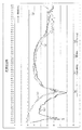
- FIG. 4 is a graph showing standard characteristics of return loss when the first antenna device configured in the first embodiment is a normal model.
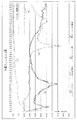
- FIG. 11 is a graph illustrating standard characteristics of return loss when the first antenna device configured in the second embodiment is an NFC model.
- FIG. 9 is a graph showing comparative characteristics representing the effect of the tuning plate of the first antenna device. It is a graph which shows the comparative characteristic showing the effect by the tuning plating plate of a 1st antenna device.
- FIGS. 1A and 1B are perspective views showing the appearance of an antenna device according to a first embodiment of the present invention.
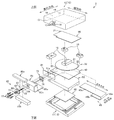
- FIG. 2 is an exploded perspective view of the antenna device according to the first embodiment of the present invention.
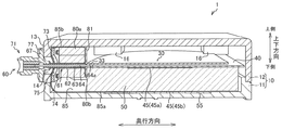
- FIG. 3 is a perspective view showing a cross section of the antenna device cut along the signal input member.
- FIG. 4 is a perspective view showing a cross section of the antenna device cut by a surface along the signal input member and a surface orthogonal to the surface.
- the antenna device according to the present embodiment is characterized in that an insulator is inserted between the antenna element and the tuning plate.
- the side from which the electromagnetic wave is radiated is referred to as the upper side (upper surface) or the front side (front surface), and the opposite side is referred to as the lower side (lower surface) or the back side (back surface).
- the extending direction of the coaxial connector is referred to as a depth direction, and a direction perpendicular to the vertical direction and the depth direction is referred to as a width direction.
- the antenna device 1 includes a case 10 that forms a hollow housing portion that houses each constituent member.
- the case 10 includes a substantially rectangular base 11 and an upper cover 12 fixed to the base 11 with screws.
- One side plate 13 extending in the width direction of the upper cover 12 has a coaxial member insertion hole 14 through which the signal input member 61 of the coaxial connector 60 is inserted, and an insertion hole for fixing the coaxial connector 60 to the side plate 13 with screws. 15 are formed through.
- a semi-disc-shaped (or bow-shaped) antenna element 30 is accommodated inside the case 10.
- a first insulating plate 40 that insulates the antenna element 30 from other members, a tuning plate 45 that functions as a short stub, and a radio wave absorber having a predetermined thickness t
- the body 50 and the tuning plating plate 55 are sequentially laminated.
- Reference numeral 16 in the figure is an element guide for positioning the antenna element 30 in the case 10.
- FIG. 5 is a perspective view of the antenna element assembled to the antenna device as viewed from the back side.
- the antenna element 30 has a shape obtained by removing a smaller bow-shaped portion from two bow-shaped portions formed by cutting a copper plate into two with a single chord 31 from a circular copper plate.
- the antenna element 30 includes an arc peripheral edge portion 32 at least at a part of the peripheral edge portion, and includes a feeder 33 at a part of the arc peripheral edge portion 32.
- the antenna element 30 includes a chord 31 that connects between the end points of the circular arc peripheral part 32 at the other part of the peripheral part.
- the length of the string 31 is about 59 mm.
- the central angle of the antenna element 30 (the central angle with respect to the arc peripheral portion 32) is larger than 180 degrees and is about 245 degrees.
- the antenna element 30 has a feeding portion 33 at an appropriate position on the circular arc peripheral portion 32, more specifically, at the center of the circular arc peripheral portion 32.
- the size of the antenna element 30 was determined in consideration of the effect of shortening the wavelength due to the dielectric constant of the radio wave absorber. Assuming that the radio wave absorber is polyurethane, when a wavelength shortening coefficient of 0.45 when the dielectric constant is 5 is reflected in ⁇ / 4 of 600 MHz, the shortened wavelength becomes 56 mm. Therefore, a circle having a diameter of 56 mm was used as an initial shape. From the results of experiments in which the diameter was gradually increased from this circle, the final diameter of the circle was 70 mm.
- chord 31 the bow-shaped portion is removed to form a straight edge (chord 31).
- the size of the chord 31 is approximately ⁇ / 4 of 600 MHz, and the size that reflects the shortening factor is determined from experiments. Since the characteristics were the best, the string 31 had a size of about 59 mm.
- the first insulating plate 40 is made of an insulating synthetic resin such as an acrylic plate or a PVC plate.
- the first insulating plate 40 plays a role of insulating the antenna element 30 and the radio wave absorber 50.
- the first insulating plate 40 is set to have such a size that the antenna element 30 and the tuning plate 45 are not electrically connected to each other and can reliably maintain an insulating state.
- the tuning plate 45 functions as a stub (short stub) for performing impedance matching by capacitively coupling with the antenna element 30 according to the area facing the antenna element 30.
- the tuning plate 45 is opposed to the back side of the antenna element 30 in an insulated state.
- the tuning plate 45 is formed of a thin plate-shaped conductor longer than the maximum diameter (maximum width) of the antenna element 30. More specifically, the tuning plate 45 has a substantially strip shape and is made of a brass foil (brass foil, conductor) having a length in the longitudinal direction of 115 mm, a length in the width direction of 25 mm, and a thickness of 0.05 mm.
- a region facing the back surface of the antenna element 30 via the first insulating plate 40 is a capacitive coupling portion 45a.
- the extra length portions (45b, 45c) of the tuning plate 45 are folded back to the back surface side of the radio wave absorber 50 via the side surface portions of the radio wave absorber 50.
- a ground portion 45 b that is electrically connected to the tuning plating plate 55 is provided in a surplus portion that is folded back on the back surface side of the radio wave absorber 50.
- the ground portion 45b faces the back surface of the radio wave absorber 50.
- a connecting portion 45c that connects the capacitive coupling portion 45a and the ground portion 45b is provided between the capacitive coupling portion 45a and the ground portion 45b.
- the tuning plate 45 is curved and deformed into a J-shape or a U-shape, or bent into a square U-shape, so that the capacitive coupling portion 45a and the ground portion 45b are connected to the front side and the back side of the radio wave absorber 50. , And the radio wave absorber 50 is sandwiched in the thickness direction.
- the capacitive coupling portion 45a faces the back surface of the antenna element 30 via the first insulating plate 40, and the ground portion 45b provided at the other end in the longitudinal direction directly faces the surface of the tuning plating plate 55. .
- the capacitive coupling portion 45a is capacitively coupled to the antenna element 30.
- the amount of capacitive coupling (tuning frequency or resonance frequency) between the tuning plate 45 and the antenna element 30 can be adjusted.
- the capacitive coupling portion 45a faces the antenna element 30 over the entire area in the width direction of the antenna element 30.
- the longitudinal length of the capacitive coupling portion 45a is set to have a length substantially equal to or longer than the diameter of the antenna element 30. Accordingly, the amount of capacitive coupling with the antenna element 30 is adjusted by the length in the short direction of the capacitive coupling portion 45a (the length in the depth direction of the antenna device 1).
- an impedance chart (see FIG. 17) is used. Impedance matching is performed on a 50 ⁇ coaxial cable according to a known matching strategy method.
- the tuning frequency of the tuning plate 45 according to the present embodiment is set to 1.3 GHz to 4.5 GHz
- the longitudinal length of the tuning plate 45 is 115 mm
- the longitudinal length of the capacitive coupling portion 45a is 74 mm
- the width direction length is It can be set as 25 mm.
- the radio wave absorber 50 is disposed on the back side of the capacitive coupling portion 45a of the tuning plate 45.
- the radio wave absorber 50 absorbs and attenuates radio waves radiated from the back side of the antenna element 30.
- the radio wave absorber 50 is made of foamed polyurethane in which carbon powder is dispersed and foamed.
- the radio wave absorber 50 has a size (area) that covers the entire surface of the antenna element 30.
- the radio wave absorption characteristics of the radio wave absorber 50 are determined by its thickness t.
- the radio wave absorber 50 only needs to have a performance of absorbing radio waves in the entire frequency range to which the antenna device 1 can (match).
- the radio wave absorber 50 may be ECOSORB AN74 (thickness 19 mm, corresponding frequency 500 MHz to 9 GHz) manufactured by E & C Engineering Co., Ltd.
- the radio wave absorber 50 can reduce the return loss characteristic of the antenna device 1 over the entire frequency range (matchable) to which the antenna device 1 corresponds. Play a role to improve. Further, since the radio wave absorber 50 has a certain degree of elasticity, the radio wave absorber 50 is compressed in the up and down direction of the antenna device 1 at the time of assembling, thereby preventing displacement of each member assembled inside the case 10. Fulfill. For example, by compressing the radio wave absorber 50 made of a foam having a thickness of about 20 mm by about 2 mm and assembling it in the case 10, it is possible to effectively prevent misalignment of other members incorporated in the case 10. Can be.
- the tuning plating plate 55 is disposed on the back side of the radio wave absorber 50. A part of the upper surface of the tuning plating plate 55 is directly opposed to and contacts the rear surface of the radio wave absorber 50, and the other portion is one end in the longitudinal direction of a ground portion 45 b of the tuning plate 45 and a ground plate (ground member) 85 described later. It faces the back surface of the radio wave absorber 50 via the portion 85a.
- the tuning plating plate 55 is electrically connected to the ground portion 45b of the tuning plate 45 by making surface contact with the ground portion 45b, and is electrically connected by making surface contact with one end portion 85a of the ground plate 85 in the longitudinal direction.
- the tuning plating plate 55 a metal plating film is formed on the upper surface of a rectangular flat plate made of ABS resin which is a synthetic resin. This metal plating film is a vacuum nickel vapor deposition plating film.
- the tuning plating plate 55 has a square shape with one side of 48 mm and a thickness of 1 mm.
- the tuning plating plate 55 is capacitively coupled to the antenna element 30 via the tuning plate 45, and mainly serves to tune electromagnetic waves in a relatively low frequency band of 600 MHz to 1.5 GHz. From the results of experiments, it is sufficient for the tuning plating plate 55 to fulfill the above role if the tuning plating plate 55 is arranged so that 85% or more of its area is located immediately below the antenna element 30. Further, the tuning plating plate 55 plays a role of a shield for preventing radio wave leakage from the lower surface of the antenna device 1 to the outside.
- the antenna device 1 includes a coaxial connector 60 having a signal input member 61 in which a center conductor 64 is electrically and mechanically fixed to the feeding portion 33 of the antenna element 30, and a cloth-like conductor at least on an outer peripheral portion (outer surface).
- a grounding plate (grounding member) 85 that comes into contact with the grounding portion 45b.
- a second insulating plate 81 for insulating both is inserted.
- a slit 81a is formed in the vertical direction to allow the center conductor 64 of the signal input member 61 to pass from the side plate 13 toward the antenna element 30.
- the coaxial connector 60 includes a signal input member 61 disposed at one end in the axial direction, a flange 67 disposed at an intermediate portion in the axial direction and electrically connected to the outer conductor 62 of the signal input member 61, and a coaxial connector 60 disposed at the other end in the axial direction. And a connector portion (coaxial receptacle) 71 which is electrically connected to each conductor of the signal input member 61 and detachably connects the transmission cable.
- the signal input member 61 is a semi-rigid coaxial member, and is inserted into the case 10 through the coaxial member insertion hole 14.
- the outer conductor 62 of the signal input member 61 is formed of a seamless metal cylinder.
- a central conductor 64 is accommodated in the hollow portion of the outer conductor 62 via an insulator 63 such as a fluororesin or polyimide.
- the outer conductor 62 of the signal input member 61 is made of copper, and the center conductor 64 is a silver-plated copper-coated steel wire.
- One end portion 64a of the central conductor 64 in the axial direction projects outward beyond one end edge of the outer conductor 62 in the axial direction.
- the outer conductor 62 surrounds the center conductor 64 at the other end in the axial direction.
- One axial end portion 64 a of the central conductor 64 exposed to the outside is fixed to the power supply portion 33 provided on the back surface of the antenna element 30 by soldering.
- the axial direction of the signal input member 61 extends in the depth direction with respect to the antenna device 1.
- the signal input member 61 extends in the direction along the tangent line of the circular arc peripheral portion 32 with respect to the antenna element 30, that is, in the direction orthogonal to the chord 31. It is growing.
- An insertion hole 68 through which a shaft of a screw 77 is inserted is formed at an appropriate position of the flange 67.
- the flange 67 is fixed to the side plate 13 of the upper cover 12.
- a connector plate 73 having a screw hole 74 in which a thread is formed is attached to the inner surface of the side plate 13. Further, a cable insertion portion 75 for passing the signal input member 61 is formed at an appropriate position in the plane of the connector plate 73.
- the flange 67 and the connector plate 73 are made of a conductor such as iron.
- the coaxial connector 60 inserts the shaft portion of the screw 77 into each hole in a state where the screw hole 74 of the connector plate 73 communicates with the insertion holes 15 and 68 formed in the side plate 13 and the flange portion 67, respectively. Then, it is fixed to the side plate 13 of the upper cover 12 by being screwed into the screw hole 74. Since the connector plate 73 is electrically connected to the flange 67 via the conductive screw 77, the connector plate 73 is also electrically connected to the outer conductor 62 of the signal input member 61.
- the connector section 71 is an SMA (Sub Miniature Type A) type 50 ⁇ connector, and detachably connects a transmission cable that is a coaxial cable for transmitting a high-frequency signal.
- SMA Subscribe Miniature Type A
- the inner conductor of the transmission cable and the center conductor 64 of the signal input member 61 conduct, and the outer conductor of the transmission cable and the outer conductor 62 of the signal input member 61 conduct.
- the ground plate 85 is a means for improving VSWR (Voltage Standing Wave Ratio) characteristics in all frequency bands (600 MHz to 6 GHz) to which the antenna device 1 according to the present embodiment corresponds.
- the ground plate 85 has a substantially rectangular shape and is made of brass foil (brass foil) having a thickness of 0.05 mm.
- the length of the ground plate 85 in the width direction is 45 mm, which is the same as the length of the conductive cushion 80 in the width direction.
- the length (longitudinal length) of the ground plate 85 in the direction orthogonal to the width direction is such that the ground plate 85 can directly or indirectly ground the conductive cushion 80, the tuning plating plate 55, and the tuning plate 45. Is set to
- Part of the ground plate 85 (in this example, the middle portion in the longitudinal direction) is disposed between the inner surface of the side plate 13 and the connector plate 73, and is screwed to the connector plate 73 together with the side plate 13 and the flange 67 by screws 77. The position is fixed in the case 10 by being fastened together.
- the ground plate 85 is in close contact with the connector plate 73, so that the ground plate 85 is electrically connected to the outer conductor 62 of the signal input member 61 via the screw 77.
- the grounding plate 85 is bent or bent at an appropriate position in the longitudinal direction at the time of assembling, so that the grounding plate 85 has a posture in which it is roughly J-shaped, L-shaped, U-shaped, or square U-shaped in the case 10.
- one end portion 85a of the earth plate 85 in the longitudinal direction makes surface contact with the surface of the tuning plating plate 55 and an appropriate portion of the earth portion 45b of the tuning plate 45, and the other end portion 85b of the longitudinal direction contacts the conductive cushion 80.
- the other end 85b in the longitudinal direction is set to a length that does not protrude beyond the second insulating plate 81 toward the antenna element 30. That is, the ground plate 85 does not face the upper surface of the antenna element 30.
- the conductive cushion 80 (80a, 80b) is electrically connected to the outer conductor 62 by holding the outer conductor 62 of the signal input member 61 between the upper and lower directions.
- the conductive cushion 80 is pressed by the outer conductor 62 and deformed, thereby playing a role of stabilizing the vertical position of the signal input member 61 inside the antenna device 1.
- the conductive cushion 80 is formed by using a foam material that can be elastically deformed as a core material and integrating a conductive cloth material with the outer peripheral portion thereof.
- the foam is desirably made of an insulator such as foamed polyurethane, foamed chloroprene rubber, and rubber sponge.
- a conductive urethane worm or the like can be used for the foam.
- the conductive cloth material is, for example, a mesh-shaped conductor formed by weaving or knitting metal fibers, and can be formed, for example, from a metal wire obtained by plating nickel on copper. Note that the conductive cloth material may be a non
- the conductive cushion 80 is arranged so that its longitudinal direction extends in a direction intersecting with the axial direction of the signal input member 61 (a direction substantially orthogonal to the axis), that is, in a width direction of the antenna device 1.
- the tuning frequency of the conductive cushion 80 can be adjusted by the length of the conductive cushion 80 in the width direction of the antenna device 1.
- an impedance chart (see FIG. 17) was used. Impedance matching is performed on the 50 ⁇ coaxial cable according to a well-known matching strategy.
- the conductive cushion 80a disposed above the signal input member 61 can have a thickness (length in the vertical direction) of 4 mm ⁇ width (length in the depth direction) of 10 mm ⁇ length of 45 mm.
- the conductive cushion 80b disposed on the side can be 8 mm thick ⁇ 10 mm wide ⁇ 45 mm long.
- the tuning frequency of the conductive cushion 80 is 4.5 GHz to 6 GHz.
- the antenna device 1 has a wavelength (600 MHz to 6 GHz) corresponding to the (matchable) wavelength / 4 (125 mm to 12.5 mm) with respect to the wavelength in consideration of the wavelength shortening.
- a sufficiently large antenna element 30 was employed, and a member for improving return loss characteristics was attached according to each frequency band.
- the tuning plating plate 55 mainly improves return loss characteristics in the 600 MHz to 1.5 GHz band
- the tuning plate 45 mainly improves return loss characteristics in the 1.3 GHz to 4.5 GHz band.
- 80 mainly improves the return loss characteristic in the 4.5 to 6 GHz band.
- the radio wave absorber 50 improves the return loss characteristics in the 500 MHz to 9 GHz band.
- the member for improving the return loss characteristic according to each frequency band it is possible to perform radio wave measurement in a wide frequency band with one antenna device. Further, the matching is performed by utilizing the dielectric constant, whereby the wavelength is shortened, and the antenna device can be downsized.
- FIGS. 6A and 6B are perspective views showing the appearance of an antenna device according to a second embodiment of the present invention.
- FIG. 7 is an exploded perspective view of the antenna device according to the second embodiment of the present invention.
- the antenna device according to the present embodiment is characterized in that it has an NFC board that performs wireless communication based on NFC (Near Field Communication).
- NFC Near Field Communication
- the antenna device 2 includes an NFC board 90 disposed above (front side) the antenna element 30.
- the NFC board 90 is housed in the case 10 in a non-contact state with the antenna element 30 by being sandwiched between the element guide 16 and the upper surface plate 17 of the upper cover 12.
- the NFC board 90 is provided with a USB (Universal Serial Bus) terminal 91 as a connection terminal for wired communication at an appropriate position at the edge.
- the USB terminal 91 is exposed to the outside via a USB terminal hole 19 formed through an arbitrary side plate 18 of the upper cover 12.
- the NFC board 90 is a communication board that performs short-range wireless communication in a frequency band different from the frequency band radiated by the antenna element 30.
- the NFC board 90 is interposed between an information processing device such as a personal computer that can be connected to the USB terminal 91 and a wireless communication terminal that can perform communication by NFC.
- the wireless communication terminal is a device that transmits and receives information wirelessly, such as a mobile phone, a smartphone, and a Wi-Fi router, and uses any of the frequency bands (600 MHz to 6 GHz included in the antenna device 2) using the antenna device 2. (Frequency range).
- the information processing device when performing a communication test in each frequency band (any band within the range of 600 MHz to 6 GHz) using the antenna device 2, transmits a communication result from the wireless communication terminal by NFC. Acquisition and transmission of an instruction from the information processing apparatus to the wireless communication terminal to generate a radio wave according to the test content by NFC can be performed.
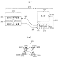
- FIG. 8A is a block diagram showing an antenna system and a measurement system using the antenna device according to one embodiment of the present invention
- FIG. 8B is a perspective view showing a calibration kit used for calibrating the measurement system. It is.
- the antenna system 300 illustrated in FIG. 8A includes a pair of antenna devices, each of which is referred to as a first antenna device 301 and a second antenna device 303. The signal is received by the second antenna device 303 which is arranged to face the radiation direction of one antenna device 301.
- the measurement system 310 includes a network analyzer 315 and a monitor 313, connects a coaxial cable 307 between a terminal P1 of the network analyzer 305 and a connector of the first antenna device 301, and connects a terminal P2 and a A coaxial cable 309 is connected between the connector and the connector. Further, a monitor cable 311 is connected between the monitor terminal 305m of the network analyzer 315 and the terminal 313m of the monitor 313.
- the network analyzer 315 uses, for example, MS46322B manufactured by Anritsu Corporation.
- the antenna device is arranged in close proximity (close contact) to an object to be measured, and is used, for example, to measure a radio wave radiated from the object to be measured.
- the device under test is a device that generates electromagnetic waves, such as a mobile phone and a mobile terminal.
- the device under test is a communication device (sub 6) that uses a frequency band of 600 MHz to 6 GHz.
- the measurement system 310 is suitable for measuring a coupling characteristic and a return loss characteristic between the first antenna device 301 and the second antenna device 303 provided in the antenna system 300.
- the antenna device 1 is disposed at a desired position or closely arranged with respect to the device under test, and receives the radio wave radiated from the device under test. Further, by disposing the device under test between the first antenna device 301 and the second antenna device 303, the radio wave radiated from the device under test or the device under test The degree of influence by an object can be measured.
- a calibration kit 320 shown in FIG. 8B is used for calibration.
- the calibration kit 320 includes four connectors: a connector 320S (SHORT), a connector 320o (OPEN), a connector 320L (LOAD), and a connector 320T (THRU).
- SHORT a connector 320S
- OPEN a connector 320o
- LOAD connector 320L
- THRU connector 320T
- TOLSLKF50A-40 manufactured by Anritsu Corporation is used.
- FIG. 9 is a flowchart showing a calibration procedure of the measurement system shown in FIG. More specifically, the figure shows a calibration procedure of the measurement system 310 performed before the measurement of the return loss characteristic and the coupling characteristic of the antenna device 1.
- a measurement frequency for example, 500 MHz to 6.2 GHz
- the network analyzer 315 is set to the calibration CAL mode.
- the connector 320S of the calibration kit is connected to the end of the coaxial cable 307 connected to the terminal P1 of the network analyzer 315, and the end of the coaxial cable 307 is short-circuited (SHORT).
- step S20 the network analyzer 315 performs an in-measurement device operation in response to a user operation.
- step S25 the connector 320o of the calibration kit is connected to the end of the coaxial cable 307 connected to the terminal P1 of the network analyzer 315, and the end of the coaxial cable 307 is opened (OPEN).
- step S30 the network analyzer 315 performs an in-measurement device operation in response to a user operation.
- step S35 the connector 320L of the calibration kit is connected to the end of the coaxial cable 307 connected to the terminal P1 of the network analyzer 315, and the load state (for example, 50 ⁇ ) is connected to the end of the coaxial cable 307 ( LOAD).
- step S40 the network analyzer 315 performs an in-measurement device operation in response to a user operation.
- step S45 the connector 320S of the calibration kit is connected to the end of the coaxial cable 309 connected to the terminal P2 of the network analyzer 315, and the end of the coaxial cable 309 is short-circuited (SHORT).
- step S50 the network analyzer 315 performs an in-measurement device operation in response to a user operation.
- step S55 the connector 320o of the calibration kit is connected to the end of the coaxial cable 309 connected to the terminal P2 of the network analyzer 305, and the end of the coaxial cable 309 is opened (OPEN).
- step S60 the network analyzer 315 performs an in-measurement device operation in response to a user operation.
- step S65 the connector 320L of the calibration kit is connected to the end of the coaxial cable 309 connected to the terminal P2 of the network analyzer 315, and the load state (for example, 50 ⁇ ) is connected to the end of the coaxial cable 309 ( LOAD).
- step S70 the network analyzer 315 performs an in-measurement device operation in response to a user operation.
- step S75 the connector 320T of the calibration kit is connected to the ends of the coaxial cables 307 and 309 connected to the terminals P1 and P2 of the network analyzer 315, and the ends of the coaxial cables 307 and 309 pass through each other (THRU).
- step S70 the network analyzer 315 performs an in-measurement device operation in response to a user operation.
- the amplitude characteristic, the return loss characteristic, the phase characteristic, and the like can be calibrated to a flat state in the set frequency band.
- FIG. 10 is a flowchart showing a return loss measuring procedure performed in the measurement system shown in FIG.
- step S105 the connector of the first antenna device 301 is connected to the end of the coaxial cable 307 connected to the terminal P1 of the network analyzer 315, and the measurement is enabled.
- step S110 the network analyzer 315 performs an in-meter operation in response to a user operation, and displays the return loss on the monitor 313. At this time, the power during the sweep of the frequency band output from the terminal P1 of the network analyzer 315 is reflected by the first antenna device 301, and the power returned from the first antenna device 301 is measured.
- FIG. 11 is a flowchart showing a procedure for measuring the coupling loss characteristic performed in the measurement system shown in FIG.
- step S155 the connector of the first antenna device 301 is connected to the distal end of the coaxial cable 307 connected to the terminal P1 of the network analyzer 315, and the measurement is enabled.
- step S ⁇ b> 160 the network analyzer 315 performs an operation in the measuring device, and displays the return loss of the first antenna device 301 on the monitor 313.
- the connector of the second antenna device 303 is connected to the end of the coaxial cable 309 connected to the terminal P2 of the network analyzer 315, and the measurement is enabled.
- step S170 the network analyzer 315 performs an operation in the measuring device, and displays the return loss of the second antenna device 303 on the monitor 313.
- step S175 the first antenna device 301 and the second antenna device 303 are opposed to each other and are close (close).
- step S180 the network analyzer 315 performs an operation in the measuring device, and displays the coupling characteristics between the first antenna device 301 and the second antenna device 303 and the return loss on the monitor 313.
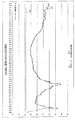
- FIG. 12 is a graph illustrating standard characteristics of return loss when the first antenna device 301 configured in the first embodiment is a normal model.
- (a) is a limit line indicating -10.9 dB
- (b) shows standard characteristics of the first antenna device 301.
- the return loss has a characteristic of -10.9 dB or more (1.8 or less for VSWR) in a frequency band of 600 MHz to 6 GHz.
- FIG. 13 is a graph showing standard characteristics of return loss when the first antenna device 301 configured in the second embodiment is an NFC model.
- 13A shows a limit line indicating -10.9 dB
- FIG. 13B shows standard characteristics of the first antenna device 301.
- the first antenna device 301 is an NFC model
- the NFC substrate 90 is formed of a double-sided substrate having a predetermined area, it affects the return loss (return loss) in the frequency band of 600 MHz to 6 GHz.
- the return loss (return loss) shows a characteristic of -10.9 dB or more (1.8 or less for VSWR).
- FIG. 14 is a graph showing a comparison characteristic indicating an effect of the tuning plate of the first antenna device 301.
- 14A shows a limit line indicating -10.9 dB
- FIG. 14B shows standard characteristics of the first antenna device 301 (with a tuning plate 45)
- FIG. 14C shows a case where the tuning plate 45 is not provided.
- D shows the characteristics when the tuning plate 45 has not been adjusted.
- the characteristic (c) when there is no tuning plate and the characteristic (d) when the tuning plate 45 is not adjusted exceed the limit line (a) of -10.9 dB in the vicinity of 500 MHz to 1 GHz.
- the standard characteristic with the tuning plate 45
- a strong resonance of ⁇ 35 dB to ⁇ 39 dB is generated around 1.9 GHz. .
- FIG. 15 is a graph showing comparative characteristics showing the effect of the tuned plating plate of the first antenna device 301.
- 15A shows a limit line indicating -10.9 dB
- FIG. 15B shows standard characteristics of the first antenna device 301 (with a tuning plating plate 55)
- FIG. (D) shows the characteristics when the entire inner surface of the base 11 is plated.
- FIG. 16 is a graph showing comparative characteristics indicating the effect of the conductive cushion of the first antenna device 301.
- 16A shows a limit line indicating -10.9 dB
- FIG. 16B shows standard characteristics of the first antenna device 301 (with the conductive cushion 80)
- FIG. The characteristics when there is no conductive cushion 80 are shown
- the graph (d) shows the characteristics when the conductive cushion 80 is loaded.
- the characteristic (c) without the conductive cushion 80 exceeds the limit line (a) of -10.9 dB in the range of 500 MHz to 6 GHz.
- the characteristic (d) when the conductive cushion 80 is loaded exceeds the limit line (a) of -10.9 dB in the vicinity of 700 MHz to 1.2 GHz, while it is -35 dB to -40 in the vicinity of 3.8 GHz to 4 GHz. A strong resonance of dB is generated.
- the standard characteristic the conductive cushion is provided
- the conductive cushion 80 provided in the first antenna device 301 is adjusted (b)
- (b) is effective in a high frequency range of 6 GHz.
- FIG. 17 is an impedance chart used for impedance matching of the antenna device 1.
- the impedance chart is used for designing RF (Radio Frequency) or microwave impedance matching.
- the horizontal axis represents the real part (resistance component) of the impedance Z, and the vertical axis represents the imaginary part (reactance component).
- the angle displayed in the surroundings is the phase ⁇ (ANG: angle) of the voltage reflection coefficient.
- the center Z0 corresponds to a state in which the load and the transmission line are matched, and is usually 50 ⁇ . However, in the impedance chart, the center is normalized to the input impedance and expressed as 1.0.
- the antenna device 1 includes an antenna element 30 having an arc peripheral edge 32 at least at a part of a peripheral edge thereof, and a feeder 33 at a part of the arc peripheral edge, and an insulation element on the back side of the antenna element.
- a tuning plate 45 which is formed of a thin plate-shaped conductor longer than the maximum diameter of the antenna element and which has a capacitive coupling portion 45a in a region facing the back surface of the antenna element;
- the radio wave absorber 50 is disposed on the back side of the capacitive coupling portion of the plate and absorbs radio waves radiated from the back side of the antenna element, and is folded back to the back side of the radio wave absorber through the side surface of the radio wave absorber.
- the tuning plating plate 55 for electrically connecting a tuning plating plate and electrically connected to the grounding member (ground plate 85), characterized in that it comprises a.
- a radio wave absorber is arranged as a member for improving the return loss characteristic of the frequency radiated from the antenna element 30 in all frequency bands, and a tuning plate and a tuning plating plate are used as members for improving the frequency characteristics in each frequency band.
- impedance matching can be achieved in the entire frequency band of 600 MHz to 6 GHz, and VSWR can be set to 1.8 or less.
- the antenna device 1 is characterized in that the tuning frequency with the antenna element 30 is adjusted by changing the area of the capacitive coupling portion 45a of the tuning plate 45. Further, the tuning frequency of the tuning plate is 1.3 GHz to 4.5 GHz. According to this aspect, by coupling the antenna element and the tuning plate capacitively, the return loss characteristic in a specific frequency band, specifically, an intermediate frequency of 1.3 GHz to 4.5 GHz can be improved and matched.
- the antenna device 1 is characterized in that the antenna element 30 and the tuning plating plate 55 are capacitively coupled via the tuning plate 45.
- the tuning frequency of the tuning plating plate is 600 MHz to 1.5 GHz. According to this aspect, by coupling the antenna element and the tuning plating plate capacitively, the return loss characteristics in a specific frequency band, specifically, a relatively low frequency of 600 MHz to 1.5 GHz can be improved and matched.
- the antenna device 1 includes a center conductor 64 whose one end in the axial direction 64a is electrically connected to the feeding unit 33, and an outer conductor surrounding the other end in the axial direction of the center conductor via the insulator 63.
- a signal input member 61 having an outer conductor and elastically deformable conductive cushions 80a and 80b sandwiching an outer conductor are provided.
- power is supplied to the antenna element 30 by the signal input member.
- the conductive cushion 80 is disposed so that the longitudinal direction extends in a direction intersecting with the axial direction of the signal input member 61, and by adjusting the longitudinal length of the conductive cushion.
- the tuning frequency with the antenna element 30 is adjusted.
- the tuning frequency of the conductive cushion is 4.5 GHz to 6 GHz. According to this aspect, the return loss characteristic at 4.5 GHz to 6 GHz can be improved by the conductive cushion.
- ground member (ground plate 85) is electrically connected to the outer conductor 62 of the signal input member 61.
- the tuning plate 45 and the tuning plated plate 55 are grounded via the ground member, and contribute to and improve the return loss characteristic in a required frequency band.
- the antenna device 2 is characterized in that the NFC board 90 is disposed on the front side of the antenna element 30.
- the NFC board is provided between an information processing device such as a personal computer that can be connected via a wired communication connection terminal such as a USB terminal provided on the NFC board, and a wireless communication terminal that can perform communication based on the NFC communication standard.
- This is a board that enables two-way communication between the two.
- the information processing device acquires a communication result from the wireless communication terminal by NFC, and the information processing device sends a communication result to the wireless communication terminal.
- an instruction can be transmitted by the NFC to generate a radio wave according to the test content.
Landscapes
- Physics & Mathematics (AREA)
- Electromagnetism (AREA)
- General Physics & Mathematics (AREA)
- Details Of Aerials (AREA)
- Waveguide Aerials (AREA)
- Control And Other Processes For Unpacking Of Materials (AREA)
- Burglar Alarm Systems (AREA)
- Radar Systems Or Details Thereof (AREA)
Abstract
Priority Applications (7)
| Application Number | Priority Date | Filing Date | Title |
|---|---|---|---|
| US17/250,502 US11417955B2 (en) | 2018-08-10 | 2018-08-10 | Antenna device |
| KR1020217006302A KR102446177B1 (ko) | 2018-08-10 | 2018-08-10 | 안테나 장치 |
| PCT/JP2018/030022 WO2020031364A1 (fr) | 2018-08-10 | 2018-08-10 | Dispositif d'antenne |
| JP2020504424A JP6703726B1 (ja) | 2018-08-10 | 2018-08-10 | アンテナ装置 |
| EP18929811.0A EP3836303B1 (fr) | 2018-08-10 | 2018-08-10 | Dispositif d'antenne |
| CN201880095872.7A CN112470340B (zh) | 2018-08-10 | 2018-08-10 | 天线装置 |
| TW107132579A TWI719345B (zh) | 2018-08-10 | 2018-09-17 | 天線裝置 |
Applications Claiming Priority (1)
| Application Number | Priority Date | Filing Date | Title |
|---|---|---|---|
| PCT/JP2018/030022 WO2020031364A1 (fr) | 2018-08-10 | 2018-08-10 | Dispositif d'antenne |
Publications (1)
| Publication Number | Publication Date |
|---|---|
| WO2020031364A1 true WO2020031364A1 (fr) | 2020-02-13 |
Family
ID=69414589
Family Applications (1)
| Application Number | Title | Priority Date | Filing Date |
|---|---|---|---|
| PCT/JP2018/030022 Ceased WO2020031364A1 (fr) | 2018-08-10 | 2018-08-10 | Dispositif d'antenne |
Country Status (7)
| Country | Link |
|---|---|
| US (1) | US11417955B2 (fr) |
| EP (1) | EP3836303B1 (fr) |
| JP (1) | JP6703726B1 (fr) |
| KR (1) | KR102446177B1 (fr) |
| CN (1) | CN112470340B (fr) |
| TW (1) | TWI719345B (fr) |
| WO (1) | WO2020031364A1 (fr) |
Cited By (3)
| Publication number | Priority date | Publication date | Assignee | Title |
|---|---|---|---|---|
| JP2022078723A (ja) * | 2020-11-13 | 2022-05-25 | 森田テック 株式会社 | 誘電率測定装置、誘電率測定方法、プログラム、及び記憶媒体 |
| JP2025530637A (ja) * | 2022-08-16 | 2025-09-17 | グーグル エルエルシー | 6GHz帯で動作可能な無線ネットワークデバイス |
| JP7805417B1 (ja) * | 2024-10-07 | 2026-01-23 | アンリツ株式会社 | 測定アンテナとそれを備える測定システム |
Families Citing this family (2)
| Publication number | Priority date | Publication date | Assignee | Title |
|---|---|---|---|---|
| WO2020106344A2 (fr) * | 2019-08-21 | 2020-05-28 | Futurewei Technologies, Inc. | Antenne à bande ultra-large à substrat unique en forme d'y et réseau d'antennes |
| RU207513U1 (ru) * | 2021-05-17 | 2021-10-29 | Алексей Васильевич Стремлин | Измеритель входного и взаимного сопротивления антенн в диапазоне частот |
Citations (8)
| Publication number | Priority date | Publication date | Assignee | Title |
|---|---|---|---|---|
| US6573867B1 (en) * | 2002-02-15 | 2003-06-03 | Ethertronics, Inc. | Small embedded multi frequency antenna for portable wireless communications |
| JP2006280009A (ja) * | 2002-11-27 | 2006-10-12 | Taiyo Yuden Co Ltd | アンテナ |
| WO2008018230A1 (fr) * | 2006-08-11 | 2008-02-14 | Konica Minolta Holdings, Inc. | Dispositif d'antenne |
| JP2008199371A (ja) | 2007-02-14 | 2008-08-28 | Fujitsu Component Ltd | Uwbアンテナ装置 |
| JP2009077238A (ja) * | 2007-09-21 | 2009-04-09 | Toshiba Corp | アンテナ装置 |
| JP2009159291A (ja) * | 2007-12-26 | 2009-07-16 | Samsung Electronics Co Ltd | アンテナ装置 |
| JP2011061758A (ja) * | 2009-08-10 | 2011-03-24 | Fujitsu Component Ltd | アンテナ装置 |
| JP2011066865A (ja) * | 2009-09-21 | 2011-03-31 | Shinko Sangyo Kk | 平面型アンテナ |
Family Cites Families (25)
| Publication number | Priority date | Publication date | Assignee | Title |
|---|---|---|---|---|
| US4628322A (en) * | 1984-04-04 | 1986-12-09 | Motorola, Inc. | Low profile antenna on non-conductive substrate |
| JP3278871B2 (ja) * | 1991-09-13 | 2002-04-30 | 株式会社デンソー | アンテナ装置 |
| JP3273463B2 (ja) * | 1995-09-27 | 2002-04-08 | 株式会社エヌ・ティ・ティ・ドコモ | 半円形放射板を使った広帯域アンテナ装置 |
| US5914695A (en) * | 1997-01-17 | 1999-06-22 | International Business Machines Corporation | Omnidirectional dipole antenna |
| FI105421B (fi) * | 1999-01-05 | 2000-08-15 | Filtronic Lk Oy | Tasomainen kahden taajuuden antenni ja tasoantennilla varustettu radiolaite |
| US6351246B1 (en) | 1999-05-03 | 2002-02-26 | Xtremespectrum, Inc. | Planar ultra wide band antenna with integrated electronics |
| WO2002001668A2 (fr) * | 2000-06-28 | 2002-01-03 | The Penn State Research Foundation | Antennes fractales bande large conformees miniatures sur substrats a constante dielectrique elevee et sur couches chirales |
| JP2002223114A (ja) * | 2000-11-22 | 2002-08-09 | Matsushita Electric Ind Co Ltd | アンテナ及びそれを用いた無線装置 |
| DE10064129B4 (de) * | 2000-12-21 | 2006-04-20 | Kathrein-Werke Kg | Antenne, insbesondere Mobilfunkantenne |
| JP3958110B2 (ja) * | 2001-06-01 | 2007-08-15 | 松下電器産業株式会社 | 逆f型アンテナ装置及び携帯無線通信装置 |
| US6670925B2 (en) * | 2001-06-01 | 2003-12-30 | Matsushita Electric Industrial Co., Ltd. | Inverted F-type antenna apparatus and portable radio communication apparatus provided with the inverted F-type antenna apparatus |
| US6842141B2 (en) * | 2002-02-08 | 2005-01-11 | Virginia Tech Inellectual Properties Inc. | Fourpoint antenna |
| JP2004328693A (ja) | 2002-11-27 | 2004-11-18 | Taiyo Yuden Co Ltd | アンテナ及びアンテナ用誘電体基板 |
| US6756932B1 (en) * | 2003-06-10 | 2004-06-29 | Raytheon Company | Microwave absorbing material |
| JP4176613B2 (ja) | 2003-10-24 | 2008-11-05 | 株式会社ワイケーシー | 超広帯域アンテナ及び超広帯域高周波回路モジュール |
| JP2005277501A (ja) | 2004-03-23 | 2005-10-06 | Amplet:Kk | Uwbアンテナ |
| TWI304664B (en) * | 2004-06-30 | 2008-12-21 | Hon Hai Prec Ind Co Ltd | Antenna |
| US7388550B2 (en) | 2005-10-11 | 2008-06-17 | Tdk Corporation | PxM antenna with improved radiation characteristics over a broad frequency range |
| KR101005285B1 (ko) * | 2008-07-18 | 2011-01-04 | 주식회사 이엠따블유 | 비흡수율 개선을 위한 안테나 장치 |
| JP4811615B2 (ja) * | 2008-11-11 | 2011-11-09 | ミツミ電機株式会社 | アンテナおよびそれを備えたアンテナ装置 |
| US8410983B2 (en) * | 2011-01-12 | 2013-04-02 | Cheng Uei Precision Industry Co., Ltd. | Wide-band antenna |
| FR2995697B1 (fr) * | 2012-09-17 | 2016-12-30 | Commissariat Energie Atomique | Dispositif de mesure de gain de capteur de champ electromagnetique |
| US9343810B2 (en) * | 2012-10-16 | 2016-05-17 | Ohio State Innovation Foundation | Method of making an extremely low profile wideband antenna |
| CN105789837A (zh) * | 2014-12-26 | 2016-07-20 | 环旭电子股份有限公司 | 用于无线通信的天线 |
| JP2020174284A (ja) * | 2019-04-10 | 2020-10-22 | 株式会社Soken | アンテナ装置 |
-
2018
- 2018-08-10 WO PCT/JP2018/030022 patent/WO2020031364A1/fr not_active Ceased
- 2018-08-10 KR KR1020217006302A patent/KR102446177B1/ko active Active
- 2018-08-10 EP EP18929811.0A patent/EP3836303B1/fr active Active
- 2018-08-10 CN CN201880095872.7A patent/CN112470340B/zh active Active
- 2018-08-10 JP JP2020504424A patent/JP6703726B1/ja active Active
- 2018-08-10 US US17/250,502 patent/US11417955B2/en active Active
- 2018-09-17 TW TW107132579A patent/TWI719345B/zh active
Patent Citations (8)
| Publication number | Priority date | Publication date | Assignee | Title |
|---|---|---|---|---|
| US6573867B1 (en) * | 2002-02-15 | 2003-06-03 | Ethertronics, Inc. | Small embedded multi frequency antenna for portable wireless communications |
| JP2006280009A (ja) * | 2002-11-27 | 2006-10-12 | Taiyo Yuden Co Ltd | アンテナ |
| WO2008018230A1 (fr) * | 2006-08-11 | 2008-02-14 | Konica Minolta Holdings, Inc. | Dispositif d'antenne |
| JP2008199371A (ja) | 2007-02-14 | 2008-08-28 | Fujitsu Component Ltd | Uwbアンテナ装置 |
| JP2009077238A (ja) * | 2007-09-21 | 2009-04-09 | Toshiba Corp | アンテナ装置 |
| JP2009159291A (ja) * | 2007-12-26 | 2009-07-16 | Samsung Electronics Co Ltd | アンテナ装置 |
| JP2011061758A (ja) * | 2009-08-10 | 2011-03-24 | Fujitsu Component Ltd | アンテナ装置 |
| JP2011066865A (ja) * | 2009-09-21 | 2011-03-31 | Shinko Sangyo Kk | 平面型アンテナ |
Non-Patent Citations (1)
| Title |
|---|
| See also references of EP3836303A4 |
Cited By (3)
| Publication number | Priority date | Publication date | Assignee | Title |
|---|---|---|---|---|
| JP2022078723A (ja) * | 2020-11-13 | 2022-05-25 | 森田テック 株式会社 | 誘電率測定装置、誘電率測定方法、プログラム、及び記憶媒体 |
| JP2025530637A (ja) * | 2022-08-16 | 2025-09-17 | グーグル エルエルシー | 6GHz帯で動作可能な無線ネットワークデバイス |
| JP7805417B1 (ja) * | 2024-10-07 | 2026-01-23 | アンリツ株式会社 | 測定アンテナとそれを備える測定システム |
Also Published As
| Publication number | Publication date |
|---|---|
| JPWO2020031364A1 (ja) | 2020-08-20 |
| JP6703726B1 (ja) | 2020-06-03 |
| KR102446177B1 (ko) | 2022-09-22 |
| US20210313690A1 (en) | 2021-10-07 |
| US11417955B2 (en) | 2022-08-16 |
| EP3836303A1 (fr) | 2021-06-16 |
| CN112470340B (zh) | 2023-05-30 |
| EP3836303A4 (fr) | 2022-03-23 |
| TWI719345B (zh) | 2021-02-21 |
| KR20210031992A (ko) | 2021-03-23 |
| EP3836303B1 (fr) | 2022-10-26 |
| TW202010175A (zh) | 2020-03-01 |
| CN112470340A (zh) | 2021-03-09 |
Similar Documents
| Publication | Publication Date | Title |
|---|---|---|
| JP6703726B1 (ja) | アンテナ装置 | |
| EP2237364B1 (fr) | Dispositif d'antenne, adaptateur de conversion et récepteur | |
| JP4792173B2 (ja) | アンテナ装置、送受信機、電気機器、及びコンピュータ端末 | |
| US20120032862A1 (en) | Antenna arrangement, dielectric substrate, pcb & device | |
| KR102305205B1 (ko) | 안테나 장치, 안테나 시스템, 및 계측 시스템 | |
| KR19990076807A (ko) | 안테나 어댑터 | |
| KR20000069255A (ko) | 안테나 어댑터 | |
| US9419340B2 (en) | Ultra wide band antenna | |
| US20110207422A1 (en) | Antenna apparatus and radio terminal apparatus | |
| Arya et al. | Compact BLE antenna with a modified PIFA configuration for wearable EMG monitor | |
| CN104737369B (zh) | 天线器件和便携式信息终端 | |
| US9160573B1 (en) | Transmission line load antenna module | |
| US20050264469A1 (en) | Antenna coupler | |
| HK40039897B (en) | Antenna device | |
| HK40039897A (en) | Antenna device | |
| KR102431624B1 (ko) | 소형 다이폴 안테나 | |
| KR101520223B1 (ko) | 전송선 로드 안테나 모듈 | |
| CN221103353U (zh) | 一种天线近场耦合测试组件及天线性能测试设备 | |
| Kim | Compact BLE Antenna with a Modified PIFA Configuration for Wearable EMG Monitor | |
| EP4734282A1 (fr) | Antenne et équipement terminal | |
| CN117039410A (zh) | 一种天线组件以及移动设备 | |
| Kabacik et al. | Foldeable wideband small antenna element | |
| Collins et al. | Handset antennas | |
| CN119050647A (zh) | 天线组件及电子设备 | |
| US20080101416A1 (en) | Broadband antenna |
Legal Events
| Date | Code | Title | Description |
|---|---|---|---|
| ENP | Entry into the national phase |
Ref document number: 2020504424 Country of ref document: JP Kind code of ref document: A |
|
| 121 | Ep: the epo has been informed by wipo that ep was designated in this application |
Ref document number: 18929811 Country of ref document: EP Kind code of ref document: A1 |
|
| NENP | Non-entry into the national phase |
Ref country code: DE |
|
| ENP | Entry into the national phase |
Ref document number: 20217006302 Country of ref document: KR Kind code of ref document: A |
|
| ENP | Entry into the national phase |
Ref document number: 2018929811 Country of ref document: EP Effective date: 20210310 |