WO2020031940A1 - 金属化フィルムおよびフィルムコンデンサ - Google Patents
金属化フィルムおよびフィルムコンデンサ Download PDFInfo
- Publication number
- WO2020031940A1 WO2020031940A1 PCT/JP2019/030651 JP2019030651W WO2020031940A1 WO 2020031940 A1 WO2020031940 A1 WO 2020031940A1 JP 2019030651 W JP2019030651 W JP 2019030651W WO 2020031940 A1 WO2020031940 A1 WO 2020031940A1
- Authority
- WO
- WIPO (PCT)
- Prior art keywords
- film
- fuse
- metal
- width
- margin
- Prior art date
- Legal status (The legal status is an assumption and is not a legal conclusion. Google has not performed a legal analysis and makes no representation as to the accuracy of the status listed.)
- Ceased
Links
Images


Classifications
-
- H—ELECTRICITY
- H01—ELECTRIC ELEMENTS
- H01G—CAPACITORS; CAPACITORS, RECTIFIERS, DETECTORS, SWITCHING DEVICES, LIGHT-SENSITIVE OR TEMPERATURE-SENSITIVE DEVICES OF THE ELECTROLYTIC TYPE
- H01G4/00—Fixed capacitors; Processes of their manufacture
- H01G4/32—Wound capacitors
Definitions
- the present invention relates to a metallized film including a metal film on a surface of a plastic film, and a film capacitor.
- a film capacitor (also referred to as a metallized film capacitor, a metallized film capacitor, a metallized organic film capacitor, etc.) formed by winding a metallized film produced by evaporating a metal on the surface of a plastic film is known.
- the film capacitor has a smaller capacity than the ceramic capacitor and the electrolytic capacitor, it has a feature that it can cope with a high voltage, has a good high-frequency characteristic, and has little dielectric loss. Therefore, film capacitors are widely used in electronic applications, in-vehicle applications, industrial applications, and the like.
- a capacitor using a metallized film in which a metal film is deposited as an electrode on a surface of a plastic film is known.
- a plurality of electrodes divided by a margin (non-evaporated portion) extending in the longitudinal direction and the width direction of a plastic film are formed, and the plurality of electrodes are connected by a fuse. A film is described.
- the fuse is gasified by Joule heat caused by a large current flowing when breakdown occurs. As a result, the electrode at the defective portion can be cut off (recovery of the insulating property).
- the fuse in order to lower the temperature by dispersing the generated gas and heat, it is preferable that the fuse easily radiates heat.
- An object of one embodiment of the present invention is to provide a metallized film having an improved fuse function.
- the present invention includes the inventions described in the following ⁇ 1> to ⁇ 4>.
- a plastic film is provided with a metal film on the surface, and the metal film is divided into a plurality of electrodes by a margin, and two or more of the plurality of electrodes are connected to each other by a fuse.
- a metallized film, wherein at least one of the electrodes connected by the fuse has a recess adjacent to the fuse and recessed in a direction in which the fuse extends.
- ⁇ 2> The metallized film according to ⁇ 1>, wherein a length of the recess is 1/5 to 1/2 of a width of a margin between two electrodes connected by the fuse.
- ⁇ 3> The metallized film according to ⁇ 1> or ⁇ 2>, wherein a width of the concave portion is 1/5 to 1/1 of a width of a margin between the two electrodes connected by the fuse.
- ⁇ 4> A film capacitor formed by winding the metallized film according to any one of ⁇ 1> to ⁇ 3>.
- the electrode has a concave portion that is adjacent to the fuse and that is recessed in the direction in which the fuse extends.
- the length of the fuse is longer than the width of the margin due to the formation of the concave portion. Therefore, according to one embodiment of the present invention, the length of the fuse can be made longer than in the case where the concave portion is not formed.
- the width of the margin can be made smaller than that of the related art, so that the effective area of the electrode can be increased.
- FIG. 1 is a schematic top view showing a configuration of a metallized film according to Embodiment 1 of the present invention. It is a top view which shows the modification of the recessed part of the metallized film which concerns on Embodiment 1 of this invention. It is a schematic top view which shows the structure of the metallized film which concerns on Embodiment 2 of this invention. It is an outline sectional view showing the composition of the metallized film concerning Embodiment 3 of the present invention.
- 1 is a schematic cross-sectional view illustrating a configuration of a film capacitor according to one embodiment of the present invention.
- FIG. 1 is a schematic top view showing the configuration of a metallized film according to Examples 1 and 2 of the present invention.
- FIG. 4 is a schematic top view showing a configuration of a metallized film according to Comparative Example 1.
- One embodiment of the present invention provides a metallized film with an improved fuse function without reducing the effective area of the electrode.
- the metallized film 5 includes a film 11 made of a metal on the surface of the plastic film 1.
- Two or more of the plurality of electrodes are connected to each other by a fuse 12, and at least one of the electrodes connected by the fuse 12 is connected to the fuse 12 adjacent to the fuse 12.
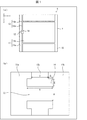
- FIG. 1A is a schematic top view showing the configuration of the metallized film 5 according to the first embodiment of the present invention
- FIG. 1B is an enlarged view of the periphery of the fuse 12.
- the direction perpendicular to both the longitudinal direction and the thickness direction is referred to as “width direction”
- the longitudinal dimension is referred to as “length”
- the width direction is referred to as “length”. Width.
- the direction in which the fuse connects the electrodes is called the "extension direction”
- the dimension in the extension direction is simply “length”
- the direction perpendicular to both the extension direction and the thickness direction is the "width direction”
- the dimension in the width direction is Called "width”.
- FIG. 1A is a diagram showing a part of the metallized film 5 in the longitudinal direction.
- the metallized film 5 is actually a long object extending in the y-axis direction.
- the metal film 11 is divided into a strip electrode 11a and small electrodes 11b by a margin 13a extending in the longitudinal direction of the metallized film 5. Also, a plurality of small electrodes 11b are provided, and each is divided by a margin 13b extending in the width direction of the metallized film 5. A band-shaped margin 15 is formed at the end of the metallized film 5 opposite to the end where the band-shaped electrode 11a exists.
- the strip electrode 11a and the small electrode 11b are connected by a fuse 12.
- Each of the strip-shaped electrode 11 a and the small electrode 11 b has a concave portion 14 which is adjacent to the fuse 12 and is depressed in the extending direction of the fuse 12.
- the length A of the fuse 12 is longer than the width C of the margin 13a due to the formation of the concave portion 14. Therefore, in the metallized film 5, the length of the fuse can be made longer than in the case where no concave portion is formed. Therefore, in the metallized film 5, the fuse can be easily dissipated heat without reducing the effective area of the electrode as compared with the related art. Therefore, according to one embodiment of the present invention, it is possible to provide a metallized film having an improved fuse function without reducing the effective area of the electrode.
- the plastic film 1 As the plastic film 1 according to one embodiment of the present invention, a general plastic film used for a conventional metallized film can be used. Specifically, the plastic film 1 is preferably a biaxially stretched polypropylene (PP) film, a polyethylene terephthalate (PET) film, or the like. The plastic film 1 may be a laminate.
- PP polypropylene
- PET polyethylene terephthalate
- the thickness of the plastic film 1 is not particularly limited, but is preferably 1 ⁇ m to 20 ⁇ m, and more preferably 2 ⁇ m to 10 ⁇ m.
- the size of the plastic film 1 may be set according to the use of the film capacitor, the width is preferably 10 mm to 150 mm, more preferably 40 mm to 120 mm, and the length is preferably 10 m to 2000 m, and 100 m to 1000 m. Is more preferred. That is, the plastic film 1 is preferably long so that the metallized film 5 can be wound to form a film capacitor.
- the film 11 made of a metal has a function as an electrode.
- the metal aluminum, magnesium, metal silicon, zinc, tin, indium, copper, iron, nickel, at least one metal selected from the group consisting of chromium is preferable, aluminum, magnesium, metal silicon, zinc, tin, At least one metal selected from the group consisting of indium is more preferred.
- the film 11 made of a metal may be a film made of a single metal or a film made of a plurality of types of metals. Further, the film 11 made of metal may be a single layer or a plurality of layers (laminated body).
- the method for forming the metal film 11 is not particularly limited, but is preferably formed by vapor deposition.
- the metal film 11 can be formed by vacuum deposition using a known deposition apparatus.
- the metallized film 5 has a region where the film 11 made of metal is not formed. This area is called a “margin”.
- the margin can be formed, for example, by masking when depositing a metal on the plastic film 1.
- the metal film 11 is divided into a strip electrode 11a and a small electrode 11b by a margin 13a extending in the longitudinal direction of the metallized film 5 and a margin 13b extending in the width direction of the metallized film 5.
- the strip-shaped electrode 11a is formed at one end in the width direction of the metallized film 5, and extends continuously in the longitudinal direction of the metallized film 5.
- an external electrode can be connected to the strip electrode 11a.
- a plurality of small electrodes 11b are provided and each is separated by a margin 13b extending in the width direction of the metallized film 5.
- the width of the margin 13 for dividing the electrode is preferably 0.2 to 2 mm, more preferably 0.4 to 1 mm, from the viewpoint of the effective area of the electrode.
- the width of the strip electrode 11a is preferably 1 to 10 mm, and more preferably 2 to 5 mm.
- the width of the small electrode 11b is preferably 5 to 100 mm, more preferably 10 to 50 mm.
- the strip electrode 11a and the small electrode 11b are connected by a fuse 12.
- the fuse is preferably formed integrally with the strip electrode 11a and the small electrode 11b by vapor deposition or the like.
- the metal constituting the fuse is preferably at least one metal selected from the group consisting of aluminum, magnesium, metal silicon, zinc, tin, indium, copper, iron, nickel and chromium.
- the fuse 12 when a dielectric breakdown occurs in a film capacitor formed by winding the metallized film 5, a large current flows, so that the fuse 12 is heated by Joule heat. As a result, the temperature of the fuse 12 increases, and the metal contained in the fuse 12 is gasified. As a result, the fuse 12 loses its electronic conductivity as a metal. When the generated gas and heat are dispersed, the temperature decreases, and the gas loses its electrical conductivity. As a result, the electrode at the defective portion can be cut off (recovery of the insulating property). That is, the film capacitor can have self-healing properties (self-healing). Thereby, in the film capacitor formed by winding the metallized film 5, the decrease in the capacity can be kept small, the life and the self-security can be improved, and the reliability is improved.
- the length A of the fuse 12 is preferably from 0.2 to 4 mm, more preferably from 0.4 to 2 mm, and still more preferably from 0.6 to 2 mm, from the viewpoint of the fuse function.
- the width B of the fuse 12 is preferably 0.2 to 2 mm, more preferably 0.4 to 1 mm.
- the length A of the fuse 12 can be determined in consideration of a margin width necessary for maintaining electrical insulation at a margin between a defective part and a healthy part.
- a margin width necessary for maintaining electrical insulation at a margin between a defective part and a healthy part For example, in Example 1 described below, a biaxially stretched polypropylene film having a thickness of 5 ⁇ m is used. The DC breakdown voltage of a capacitor using this film is about 2500V. When insulation breakdown occurs at 2500 V DC, the margin width required to separate the electrode at the defective part and maintain electrical insulation at the margin between the defective part and the healthy part is about 1 mm. A suitable fuse length for a margin width of 1 mm is 2 mm.
- the recess 14 is recessed adjacent to the fuse 12 in the direction in which the fuse 12 extends. In other words, the recess 14 is recessed along the side of the fuse 12 in the direction in which the fuse 12 extends.
- the recess 14 can be said to be a region formed by the side of the fuse 12 and one side of the strip-shaped electrode 11a and the small electrode 11b. Due to the presence of the recess 14, the end of the margin 13a in contact with the fuse 12 is L-shaped or T-shaped when viewed from a direction perpendicular to the surface of the metallized film 5 (z-axis direction). From the viewpoint of uniform heat dissipation, the concave portions 14 are preferably formed symmetrically.
- the end of the margin 13a in contact with the fuse 12 is T-shaped. More preferably, the recess 14 is formed to be line-symmetric and point-symmetric. In this case, the fuse 12 is sandwiched between T-shaped ends of the margin 13a as shown in FIG. From the viewpoint that at least the length of the fuse 12 needs to be longer than the width of the margin 13a, the concave portion 14 may be asymmetric. In this case, the end of the margin 13a that contacts the fuse 12 may be L-shaped. Good.
- the dimension of the concave portion parallel to the extension direction of the fuse that is, the depth of the concave portion of the concave portion is referred to as “the length of the concave portion”.
- the dimension of the recess parallel to the width direction of the fuse is referred to as “width of the recess”.
- the length D of the recess 14 is preferably 1/10 to 1/1, and more preferably 1/5 to 1/2 of the width C of the margin 13a.
- the width E of the recess 14 is preferably 1/10 to 1/1, more preferably 1/5 to 1/1, and more preferably 1/5 to 1/2 of the width C of the margin 13a. More preferably, there is.
- the margin 13a to be compared with the dimension of the concave portion 14 is a margin in contact with the fuse 12, and can be said to be a margin between two electrodes connected by the fuse 12.
- the gasification of the fuse 12, the dispersion of gas and heat, the decrease in temperature, the increase in resistance, and the recovery of insulating property at the time of the occurrence of dielectric breakdown proceed simultaneously and uniformly throughout the fuse 12.
- the current when the dielectric breakdown occurs flows uniformly through the fuse 12.
- the width B of the fuse 12 wider than the width C of the margin 13a.
- the length A of the fuse 12 shorter than the width B of the fuse.
- the film resistance around the fuse 12 is more preferably 2 to 5 ⁇ / ⁇ as described later.
- the film resistance value is 3 ⁇ / ⁇
- the resistance value of the fuse reaches 3 ⁇ A / B ⁇ .
- the film resistance around the small electrode is more preferably 40 to 50 ⁇ / ⁇ as described later.
- the film resistance is 50 ⁇ / ⁇
- the length D of the concave portion 14 and the width E of the concave portion 14 be in the above-described ranges.
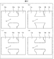
- FIG. 2 is a top view showing a modified example of the recess 14.
- the recess 14a shown in FIG. 2A is semicircular. In FIG. 2A, it can be said that the end of the margin 13 a in contact with the fuse 12 has a width that increases in a curve toward the fuse 12 and then decreases.
- the recess 14b shown in FIG. 2B is triangular. In FIG. 2B, it can be said that a straight line increases toward the fuse 12 at the end of the margin 13a in contact with the fuse 12.
- FIG. 2C has a shape in which a sector and a rectangle are combined.
- FIG. 2C it can be said that the end of the margin 13a in contact with the fuse 12 is constant after the width increases in a curved manner toward the fuse 12.
- the recess 14d shown in FIG. 2D has a shape in which a triangle and a rectangle are combined.
- FIG. 2D it can be said that the end of the margin 13a in contact with the fuse 12 is constant after its width linearly increases toward the fuse 12.
- the recess is rectangular and the sum of the width B of the fuse 12 and the width E of the recess 14 is uniform.
- the fuse is gasified by Joule heat associated with the flow of a large current, and loses electron conductivity as a metal.
- the resulting hot gas has electrical conductivity as an arc or plasma.
- the recess is triangular or fan-shaped, gasification of the fuse starts from the point where the sum of the width B of the fuse and the width E of the recess becomes the smallest, and the evaporation proceeds in a substantially circular shape.
- the recess is rectangular, gasification of the fuse starts and proceeds simultaneously for the entire fuse including the rectangular recess. In this case, since the resistance increases due to the dispersion of the generated gas and heat and the decrease in temperature, the insulation is restored over the entire length of the fuse. Therefore, even when used at a higher voltage, it can function as a fuse.
- the margins 13a and 13b extending in the longitudinal direction and the width direction of the metallized film 5 are formed.
- the extending direction of the margin and the direction in which the electrodes are divided are not limited thereto.
- the band-shaped margin 15 is formed at the end opposite to the end where the band-shaped electrode 11 a exists in the width direction of the metallized film 5, and extends continuously in the longitudinal direction of the metallized film 5. The presence of the band-shaped margin 15 can prevent a short circuit even when an external electrode is connected to a film capacitor formed by winding the metallized film 5.
- the film resistance of the metal film 11 is not particularly limited, it is preferably 1 to 10 ⁇ / ⁇ ( ⁇ square), more preferably 2 to 5 ⁇ / ⁇ , around the fuse 12. In the vicinity of the small electrode 11b, it is preferably 6 to 60 ⁇ / ⁇ , and more preferably 40 to 50 ⁇ / ⁇ .
- the thickness of the metal film 11 is about 3 nm to 20 nm, and preferably about 5 nm to 8 nm (about 50 metal atom layers).
- the film capacitor according to one embodiment of the present invention can be configured by stacking and winding two metallized films according to one embodiment of the present invention.
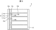
- the metal film 11 is divided into a strip electrode 11a and a small electrode 11c by a margin 13a extending in the longitudinal direction of the metallized film 6.
- the small electrode 11c and the small electrode 11d are divided by a margin 13c extending in the longitudinal direction of the metallized film 6.
- a plurality of small electrodes 11c and 11d are provided, and each is divided by a margin 13b extending in the width direction of the metallized film 6.
- the strip electrode 11a and the small electrode 11c are connected by a fuse 12a.
- Each of the strip electrode 11a and the small electrode 11c has a concave portion 14e which is adjacent to the fuse 12a and is depressed in the extending direction of the fuse 12a.
- the small electrode 11c and the small electrode 11d are connected by a fuse 12b.
- Each of the small electrode 11c and the small electrode 11d has a recess 14f that is adjacent to the fuse 12b and that is depressed in the extending direction of the fuse 12b.
- the fuses are formed double in the width direction of the metallized film 6. Thereby, the risk of causing short-circuit destruction due to malfunction or non-operation can be further reduced as compared with the first embodiment. It is preferable to provide a relatively thin fuse for the terminal small electrode (small electrode close to the strip-shaped margin 15). Therefore, the width of the fuse 12b is preferably smaller than that of the fuse 12a.
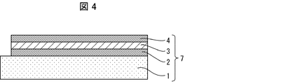
- a metallized film 7 according to Embodiment 3 of the present invention includes, on one surface of a plastic film 1, a film 2 made of a first metal having an oxide band gap of 5 eV or more, A film 3 made of a second metal having a band gap of less than 5 eV, and a film 4 made of a third metal having a band gap of an oxide of 5 eV or more.
- various metals constituting a metallized film can be classified into a metal forming an oxide having a band gap of 5 eV or more and a metal forming an oxide having a band gap of less than 5 eV.
- An oxide having a band gap of 5 eV or more is a wide-gap insulator.
- An oxide having a band gap of less than 5 eV is a narrow-gap electronic conductor.
- a metal forming an oxide having a band gap of 5 eV or more is used as the first metal and the third metal, and an oxide having a band gap of less than 5 eV is used.
- the metal to be formed is used as the second metal.
- the first metal and the third metal are preferably at least one metal selected from the group consisting of aluminum, magnesium, and metallic silicon, more preferably aluminum and magnesium, and even more preferably aluminum.
- the band gap of aluminum oxide (Al 2 O 3 ) is 8 eV
- the band gap of magnesium oxide (MgO) is 5.5 eV
- the band gap of metal silicon oxide (SiO 2 ) is 7 eV. is there.
- the films 2 and 4 when the films 2 and 4 are formed, an oxide that is a wide gap insulator is formed on the surface (interface) on the plastic film 1 side. It is formed. Therefore, injection of the carrier into the plastic film 1 can be prevented, and the carrier behavior in the plastic film 1 is reduced.
- the first metal and the third metal may be the same or different from each other, but are preferably the same.
- the film 2 made of the first metal and the film 4 made of the third metal may be a film made of a single metal, or may be a film made of a plurality of types of metals. It is preferably a film made of a single metal.
- the film 2 made of the first metal and the film 4 made of the third metal may each be a single layer or a plurality of layers (laminated body), but it is preferably one layer. .
- the second metal is preferably at least one metal selected from the group consisting of zinc, tin, and indium, more preferably zinc and tin, and even more preferably zinc.
- the band gap of zinc oxide (ZnO) is 3 eV
- the band gap of tin oxide (SnO 2 ) is 3 eV
- the band gap of indium oxide (In 2 O 3 ) is 3 eV.
- the film 3 made of the second metal gradually forms an oxide from its end (exposed portion) by an anodic oxidation reaction when a ripple current flows, but the oxide is a narrow gap electronic conductor,
- the film 3 made of the second metal maintains the function as an electrode.
- the film 3 made of the second metal may be a film made of a single metal or a film made of a plurality of types of metals, but is preferably a film made of a single metal. Further, the film 3 made of the second metal may be a single layer or a plurality of layers (laminated body), but is preferably a single layer.
- the method for forming the film 2 made of the first metal, the film 3 made of the second metal, and the film 4 made of the third metal is not particularly limited, but is preferably formed by vapor deposition. These films 2 to 4 can be formed by vacuum evaporation using a known evaporation apparatus.
- the total film resistance of the active portions (portions functioning as electrodes) in the films 2 to 4 made of the first to third metals is not particularly limited, but is preferably 6 to 60 ⁇ / ⁇ ( ⁇ square). , 40 to 50 ⁇ / ⁇ .
- the total thickness of the first to third metal films 2 to 4 is about 3 nm to 20 nm, preferably about 5 nm to 8 nm (about 50 metal atom layers).
- electrodes are formed on the end face of the plastic film 1 by, for example, thermal spraying. There is a portion where the films 2 to 4 made of metal are not formed (the width is about 2 mm). This portion corresponds to the band-like margin 15 in the first and second embodiments.
- both use in a higher electric field (potential gradient) and long life even in a use condition where a ripple current is large are achieved (simultaneously achieved).
- the metallized film 7 constituting the film capacitor that can be provided can be provided.
- the metallized film 7 according to the third embodiment of the present invention forms a laminate of the films 2 to 4 made of the first to third metals on the plastic film 1, the films 2 to 4 For example, a pattern shape having the same fuse function as in the first and second embodiments can be formed.
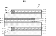
- a film capacitor 10 according to one embodiment of the present invention is configured by winding two metalized films according to one embodiment of the present invention or two sets thereof, and then winding. I have.
- the film capacitor 10 according to one aspect of the present invention is configured by, for example, winding two or two sets of the metallized film 7 according to Embodiment 3 of the present invention.
- the films 2 to 4 made of the first to third metals are sandwiched by the plastic film 1, and the film capacitor 10 is made up of the plastic film 1 / film 2 / film 3 / film 4 / plastic film 1
- the film 2 made of the first metal or the film 4 made of the third metal when the films 2 and 4 are formed, an oxide that is a wide gap insulator is formed on the surface (interface) on the plastic film 1 side. It is formed. Therefore, injection of the carrier into the plastic film 1 can be prevented, and the carrier behavior in the plastic film 1 is reduced. Therefore, the breakdown voltage of the film capacitor 10 increases.
- the ripple current flows the film 2 made of the first metal or the film 4 made of the third metal is converted into an oxide 2a, 4a which is an insulator having a wide gap by an anodic oxidation reaction. ), Thereby gradually losing the function as an electrode.
- the film 3 made of the second metal gradually forms an oxide 3a from its end (exposed portion) by an anodic oxidation reaction when a ripple current flows, but the oxide 3a is a narrow gap electronic conductor. Therefore, it becomes an electric circuit when energized, and maintains the function as an electrode. Therefore, the film capacitor 10 is prevented from decreasing in capacity even under the use condition where the ripple current is large.
- a film capacitor 10 can be provided.
- Example 1 As shown in FIG. 6A, a metallized film corresponding to the metallized film 5 according to the first embodiment of the present invention was produced.
- the plastic film 1 a biaxially stretched polypropylene film (width 50 mm, length 55 m, thickness 5 ⁇ m) was used. The plastic film was masked so that the electrode pattern shown in FIG. 6A was formed, and zinc was deposited as a metal.
- the widths of the strip electrode 11a and the strip margin 15 were each 2 mm.
- the width of the margin 13a parallel to the length direction of the plastic film and the width of the margin 13b parallel to the width direction of the plastic film were each 1 mm.
- the length of the small electrode 11b was 45 mm and the width was 29 mm.
- the width of the fuse 12 was 1 mm.
- the length of the recess 14 was 0.5 mm, and the width was 1 mm.
- the length of the fuse 12 was 2 mm.
- the fuse 12 was included in a region of about 30% from the end where the strip-shaped electrode 11a was formed, and the film resistance in this region was 3 ⁇ / ⁇ .
- the film resistance of the remaining 70% region was 50 ⁇ / ⁇ .
- Example 2 In the same manner as in Example 1, a metallized film corresponding to the metallized film 6 according to Embodiment 2 of the present invention was produced as shown in FIG. That is, in Example 2, the fuses were formed twice in the width direction. The total of the width of the small electrode 11c, the width of the margin 13c, and the length of the small electrode 11d was 45 mm. The width of the small electrode 11c was 2 mm. The width of the small electrode 11d was 9 mm. The width of the fuse 12a was 1 mm, and the width of the fuse 12b was 0.4 mm.
- the length of the recess 14e was 0.5 mm and the width was 1 mm.
- the length of the recess 14f was 0.5 mm and the width was 1 mm.
- the length of the fuse 12a was 2 mm, and the length of the fuse 12b was 2 mm.
- the fuse 12a and the fuse 12b were included in a region of about 30% from the end where the strip electrode 11a was formed, and the film resistance in this region was 3 ⁇ / ⁇ .
- the film resistance of the remaining 70% region was 50 ⁇ / ⁇ .
- a metallized film 100 shown in FIG. 7 was produced in the same manner as in Example 1.
- a strip electrode 111a, a small electrode 111b, a margin 113a extending in the longitudinal direction of the metallized film 100, a margin 113b extending in the width direction of the metallized film 100, A band-shaped margin 115 and a fuse 112 are formed, and the dimensions of each member are the same as those in the first embodiment.
- no recess was formed. Therefore, the length of the fuse 112 was 1 mm, the same as the width of the margin 113a extending in the longitudinal direction of the metallized film 100.
- the fuse 112 was included in a region about 30% from the end where the band-shaped electrode 111a was formed, and the film resistance in this region was 3 ⁇ / ⁇ .
- the film resistance of the remaining 70% region was 50 ⁇ / ⁇ .
- the film capacitor according to the present invention can be widely used as a DC capacitor in electronic applications, in-vehicle applications, industrial applications, and the like.
Landscapes
- Engineering & Computer Science (AREA)
- Power Engineering (AREA)
- Manufacturing & Machinery (AREA)
- Microelectronics & Electronic Packaging (AREA)
- Fixed Capacitors And Capacitor Manufacturing Machines (AREA)
Abstract
電極の有効面積を小さくせずにヒューズの機能を向上した金属化フィルムを提供する。金属化フィルム(5)は、プラスチックフィルム(1)の表面に金属からなる膜(11)を備え、上記金属からなる膜(11)は、マージン(13)によって複数の電極に分割されており、上記複数の電極のうちの2つ以上は、ヒューズ(12)によって互いに接続されており、上記ヒューズ(12)によって接続された電極の少なくとも1つは、上記ヒューズ(12)に隣接して上記ヒューズ(12)の延伸方向に窪んだ凹部を有する。
Description
本発明は、プラスチックフィルムの表面に金属からなる膜を備える金属化フィルム、およびフィルムコンデンサに関する。
一般に、プラスチックフィルムの表面に金属を蒸着させることによって作製された金属化フィルムを巻回してなるフィルムコンデンサ(金属蒸着フィルムコンデンサ、メタライズドフィルムコンデンサ、金属化有機フィルムコンデンサ等とも称される)が知られている。フィルムコンデンサは、セラミックコンデンサおよび電解コンデンサと比較して容量は小さいものの、高電圧に対応可能であり、高周波特性が良好で誘電体損失が少ないという特徴を備えている。それゆえ、フィルムコンデンサは、電子用途、車載用途、産業用途等に広く使用されている。特に近年、フィルムコンデンサは、ハイブリッド車(HEV)や電気自動車(EV)等の車載用途において、寿命および自己保安性に課題を有するアルミニウム電解コンデンサとの置き換え需要によって市場規模を拡大している。アルミニウム電解コンデンサの代わりにフィルムコンデンサを用いることにより、小型化(コンパクト化)、軽量化、およびコストダウンを図ることができる。
上記フィルムコンデンサとしては、従来、プラスチックフィルムの表面に電極として金属からなる膜が蒸着された金属化フィルムを用いたコンデンサが知られている。例えば、特許文献1~3には、プラスチックフィルムの長手方向および幅方向に伸びるマージン(非蒸着部)によって分割された複数の電極が形成され、これらの複数の電極がヒューズによって接続された金属化フィルムが記載されている。
ヒューズは、絶縁破壊が生じた際に大きな電流が流れることに伴うジュール熱によってガス化する。これにより、欠陥のある部位の電極を切り離す(絶縁性を回復する)ことができる。ここで、生じたガスおよび熱を分散させて温度を低下させるためには、ヒューズが放熱しやすいことが好ましい。
しかし従来技術にはヒューズの機能向上の観点から改善の余地があった。
本発明の一態様はヒューズの機能を向上した金属化フィルムを提供することを目的とする。
上記課題を解決するために、本発明は、下記<1>~<4>で示される発明を包含している。
<1> プラスチックフィルムの表面に金属からなる膜を備え、上記金属からなる膜は、マージンによって複数の電極に分割されており、上記複数の電極のうちの2つ以上は、ヒューズによって互いに接続されており、上記ヒューズによって接続された電極の少なくとも1つは、上記ヒューズに隣接して上記ヒューズの延伸方向に窪んだ凹部を有する金属化フィルム。
<2> 上記凹部の長さは、上記ヒューズによって接続された2つの電極の間のマージンの幅の1/5~1/2である、<1>に記載の金属化フィルム。
<3> 上記凹部の幅は、上記ヒューズによって接続された2つの電極の間のマージンの幅の1/5~1/1である、<1>または<2>に記載の金属化フィルム。
<4> <1>~<3>の何れか一項に記載の金属化フィルムを巻回してなる、フィルムコンデンサ。
<1> プラスチックフィルムの表面に金属からなる膜を備え、上記金属からなる膜は、マージンによって複数の電極に分割されており、上記複数の電極のうちの2つ以上は、ヒューズによって互いに接続されており、上記ヒューズによって接続された電極の少なくとも1つは、上記ヒューズに隣接して上記ヒューズの延伸方向に窪んだ凹部を有する金属化フィルム。
<2> 上記凹部の長さは、上記ヒューズによって接続された2つの電極の間のマージンの幅の1/5~1/2である、<1>に記載の金属化フィルム。
<3> 上記凹部の幅は、上記ヒューズによって接続された2つの電極の間のマージンの幅の1/5~1/1である、<1>または<2>に記載の金属化フィルム。
<4> <1>~<3>の何れか一項に記載の金属化フィルムを巻回してなる、フィルムコンデンサ。
本発明の一態様に係る金属化フィルムにおいて、電極は、ヒューズに隣接してヒューズの延伸方向に窪んだ凹部を有する。この凹部が形成されている分、ヒューズの長さはマージンの幅より長くなる。従って、本発明の一態様によれば、凹部が形成されていない場合に比べてヒューズの長さを長くすることができる。
それゆえ、本発明の一態様によれば、電極の有効面積を小さくせずにヒューズの機能を向上した金属化フィルムを提供することができるという効果を奏する。
また、本発明の一態様によれば、ヒューズの長さを従来どおりとした場合、マージンの幅を従来に比べて狭くすることができるため、電極の有効面積を大きくすることができるとも言える。
本発明の一実施形態について以下に説明するが、本発明はこれに限定されるものではない。本発明は、以下に説明する各実施形態や各構成に限定されるものではなく、特許請求の範囲に示した範囲で種々の変更が可能であり、異なる実施形態や実施例にそれぞれ開示された技術的手段を適宜組み合わせて得られる実施形態や実施例についても本発明の技術的範囲に含まれる。また、本明細書中に記載された学術文献および特許文献の全てが、本明細書中において参考文献として援用される。なお、本明細書において特記しない限り、数値範囲を表す「A~B」は、「A以上、B以下」を意味する。
放熱しやすいヒューズを得るためには、ヒューズを細長くすることが考えられる。しかしながら、上述のような従来技術では、各電極を隔てるマージンの幅と、ヒューズの長さとが同じであるため、ヒューズを長くするためにはマージンの幅を長くする必要があった。この場合、電極の有効面積が小さくなり、コストおよびサイズの点で不利になるという問題があった。これらのことから本発明者らは、上述のような従来技術では、電極の有効面積を小さくせずにヒューズの機能を向上させるという観点からは改善の余地があることを独自に見出した。
本発明の一態様は、電極の有効面積を小さくせずにヒューズの機能を向上した金属化フィルムを提供する。
〔実施形態1〕
本発明の一実施形態について、以下に説明する。
本発明の一実施形態について、以下に説明する。
図1に示すように、本発明の実施形態1に係る金属化フィルム5は、プラスチックフィルム1の表面に金属からなる膜11を備え、上記金属からなる膜11は、マージン13によって複数の電極に分割されており、上記複数の電極のうちの2つ以上は、ヒューズ12によって互いに接続されており、上記ヒューズ12によって接続された電極の少なくとも1つは、上記ヒューズ12に隣接して上記ヒューズ12の延伸方向に窪んだ凹部14を有する。図1の(a)は、本発明の実施形態1に係る金属化フィルム5の構成を示す概略の上面図であり、図1の(b)はヒューズ12の周辺を拡大した図である。
なお、以下では、金属化フィルム、プラスチックフィルム、マージン、電極に関して、長手方向および厚み方向の両方に垂直な方向を「幅方向」、長手方向の寸法を「長さ」、幅方向の寸法を「幅」と称する。ヒューズに関しては、ヒューズが電極を接続する方向を「延伸方向」、延伸方向における寸法を単に「長さ」、延伸方向および厚み方向の両方に垂直な方向を「幅方向」、幅方向の寸法を「幅」と称する。
図1の(a)では、x軸方向が金属化フィルム5の幅方向に相当し、y軸方向が金属化フィルム5の長手方向に相当する。図1の(a)は、金属化フィルム5の長手方向における一部を示した図である。金属化フィルム5は実際にはy軸方向に伸びる長尺物である。
金属からなる膜11は、金属化フィルム5の長手方向に伸びるマージン13aによって帯状電極11aと小電極11bとに分割されている。また、小電極11bは複数設けられ、それぞれ金属化フィルム5の幅方向に伸びるマージン13bによって分割されている。金属化フィルム5の幅方向において帯状電極11aが存在する端部とは反対側の端部には帯状マージン15が形成されている。帯状電極11aと小電極11bとは、ヒューズ12によって接続されている。帯状電極11aおよび小電極11bはそれぞれ、ヒューズ12に隣接してヒューズ12の延伸方向に窪んだ凹部14を有する。
図1の(b)に示すように、凹部14が形成されていることにより、ヒューズ12の長さAは、マージン13aの幅Cよりも長い。従って、金属化フィルム5では、凹部が形成されていない場合に比べてヒューズの長さを長くすることができる。そのため、金属化フィルム5では、従来に比べて電極の有効面積を小さくせずにヒューズを放熱しやすくすることができる。それゆえ、本発明の一態様によれば、電極の有効面積を小さくせずにヒューズの機能を向上した金属化フィルムを提供することができるという効果を奏する。
[プラスチックフィルム]
本発明の一態様に係るプラスチックフィルム1には、従来の金属化フィルムに用いられている一般的なプラスチックフィルムを用いることができる。具体的には、プラスチックフィルム1としては、二軸延伸されたポリプロピレン(PP)フィルムおよびポリエチレンテレフタレート(PET)フィルム等が好適である。プラスチックフィルム1は、積層体であってもよい。
本発明の一態様に係るプラスチックフィルム1には、従来の金属化フィルムに用いられている一般的なプラスチックフィルムを用いることができる。具体的には、プラスチックフィルム1としては、二軸延伸されたポリプロピレン(PP)フィルムおよびポリエチレンテレフタレート(PET)フィルム等が好適である。プラスチックフィルム1は、積層体であってもよい。
プラスチックフィルム1の厚さは、特に限定されないものの、1μm~20μmが好ましく、2μm~10μmがより好ましい。また、プラスチックフィルム1の大きさは、フィルムコンデンサの用途に応じて設定すればよいものの、幅は10mm~150mmが好ましく、40mm~120mmがより好ましく、長さは10m~2000mが好ましく、100m~1000mがより好ましい。即ち、プラスチックフィルム1は、金属化フィルム5を巻回してフィルムコンデンサを形成することができるように、長尺物であることが好ましい。
[金属からなる膜]
金属からなる膜11は、電極としての機能を有する。当該金属としては、アルミニウム、マグネシウム、金属シリコン、亜鉛、スズ、インジウム、銅、鉄、ニッケル、クロムからなる群より選択される少なくとも一種の金属が好ましく、アルミニウム、マグネシウム、金属シリコン、亜鉛、スズ、インジウムからなる群より選択される少なくとも一種の金属がより好ましい。
金属からなる膜11は、電極としての機能を有する。当該金属としては、アルミニウム、マグネシウム、金属シリコン、亜鉛、スズ、インジウム、銅、鉄、ニッケル、クロムからなる群より選択される少なくとも一種の金属が好ましく、アルミニウム、マグネシウム、金属シリコン、亜鉛、スズ、インジウムからなる群より選択される少なくとも一種の金属がより好ましい。
金属からなる膜11は、単一の金属からなる膜であってもよく、複数種類の金属からなる膜であってもよい。また、金属からなる膜11は、一層であってもよく、複数層(積層体)であってもよい。
金属からなる膜11の形成方法は、特に限定されないものの、蒸着によって形成されていることが好ましい。金属からなる膜11は、公知の蒸着装置を用いた真空蒸着によって形成することができる。
金属化フィルム5は、金属からなる膜11が形成されていない領域を有する。この領域を「マージン」と称する。マージンは、例えば、プラスチックフィルム1に金属を蒸着させる際にマスキングすることにより形成することができる。
金属からなる膜11は、金属化フィルム5の長手方向に伸びるマージン13aおよび金属化フィルム5の幅方向に伸びるマージン13bによって帯状電極11aと小電極11bとに分割されている。帯状電極11aは、金属化フィルム5の幅方向の一端に形成されており、金属化フィルム5の長手方向に連続的に伸びている。金属化フィルム5を巻回してなるフィルムコンデンサにおいて帯状電極11aに外部電極を接続することができる。小電極11bは複数設けられ、それぞれ金属化フィルム5の幅方向に伸びるマージン13bによって隔てられている。
電極を分割するマージン13の幅は、電極の有効面積の観点から、0.2~2mmであることが好ましく、0.4~1mmであることがより好ましい。帯状電極11aの幅は、1~10mmであることが好ましく、2~5mmであることがより好ましい。また、小電極11bの幅は、5~100mmであることが好ましく、10~50mmであることがより好ましい。
帯状電極11aと小電極11bとは、ヒューズ12によって接続されている。ヒューズは蒸着等によって帯状電極11aおよび小電極11bと一体として形成されていることが好ましい。また、ヒューズを構成する金属は上述のアルミニウム、マグネシウム、金属シリコン、亜鉛、スズ、インジウム、銅、鉄、ニッケル、クロムからなる群より選択される少なくとも一種の金属であることが好ましい。このように電極を分割したうえでヒューズによって接続することにより、金属化フィルム5にはヒューズ機能を備えるパターン形状が形成されている。
具体的には、金属化フィルム5を巻回してなるフィルムコンデンサにおいて絶縁破壊が生じた場合、大きな電流が流れるため、ジュール熱によってヒューズ12が加熱される。これにより、ヒューズ12の温度が上昇し、ヒューズ12に含まれる金属はガス化する。その結果、ヒューズ12は金属としての電子伝導性を失う。生じたガスおよび熱が分散すると、温度は低下するため、ガスとしての電気伝導性も失う。これにより、欠陥のある部位の電極を切り離す(絶縁性を回復する)ことができる。つまり、当該フィルムコンデンサは、自己回復性(セルフヒーリング)を備えることができる。これにより、金属化フィルム5を巻回してなるフィルムコンデンサは、容量の減少を少なく留めることができると共に、寿命および自己保安性を向上させることができ、信頼性が高まる。
ヒューズ12の長さAは、ヒューズ機能の観点から、0.2~4mmであることが好ましく、0.4~2mmであることがより好ましく、0.6~2mmであることがさらに好ましい。また、ヒューズ12の幅Bは、0.2~2mmであることが好ましく、0.4~1mmであることがより好ましい。
なお、絶縁破壊が生じた際に、ヒューズの動作が成功することにより、欠陥のある部位の電極が切り離される。ヒューズ12の長さAは、この場合に、欠陥部位と健全部位との間のマージンで電気絶縁が保たれるために必要なマージン幅を考慮して決定され得る。例えば後述の実施例1では、二軸延伸された厚さ5μmのポリプロピレンフィルムを使用している。このフィルムを使用するコンデンサの直流破壊電圧は約2500Vである。直流2500Vで絶縁破壊が生じた際に、欠陥のある部位の電極を切り離して欠陥部位と健全部位との間のマージンで電気絶縁が保たれるために必要なマージン幅は約1mmである。マージン幅1mmに対して好適なヒューズ長は2mmである。
凹部14は、ヒューズ12に隣接してヒューズ12の延伸方向に窪んでいる。換言すれば、凹部14は、ヒューズ12の側部に沿って、ヒューズ12の延伸方向に窪んでいる。凹部14は、ヒューズ12の側部、並びに帯状電極11aおよび小電極11bの一辺によって形成された領域であるとも言える。凹部14が存在するため、金属化フィルム5の面に垂直な方向(z軸方向)から見ると、マージン13aのヒューズ12に接する端部は、L字型またはT字型である。均一に放熱するという観点からは、凹部14が対称的に形成されていることが好ましく、この場合、マージン13aのヒューズ12に接する端部はT字型である。凹部14は線対称かつ点対称に形成されていることがより好ましく、この場合、ヒューズ12は図1に示されるようにマージン13aのT字型の端部に挟まれている。少なくともヒューズ12の長さがマージン13aの幅より長ければよいという観点からは、凹部14は非対称であってもよく、この場合、マージン13aのヒューズ12に接する端部はL字型であってもよい。
本明細書において、ヒューズの延伸方向に平行な凹部の寸法、すなわち、凹部の窪みの深さを「凹部の長さ」と称する。また、ヒューズの幅方向に平行な凹部の寸法を「凹部の幅」と称する。凹部14の長さDは、マージン13aの幅Cの1/10~1/1であることが好ましく、1/5~1/2であることがより好ましい。また、凹部14の幅Eは、マージン13aの幅Cの1/10~1/1であることが好ましく、1/5~1/1であることがより好ましく、1/5~1/2であることがさらに好ましい。ここで凹部14の寸法の比較対象となっているマージン13aは、ヒューズ12に接するマージンであり、ヒューズ12によって接続された2つの電極の間のマージンとも言える。
なお、絶縁破壊が生じた際の、ヒューズ12のガス化、ガスと熱の分散、温度の低下、高抵抗化、絶縁性の回復は、ヒューズ12全体で同時に均一に進むことが好ましい。そのためには、絶縁破壊が生じた際の電流がヒューズ12に均一に流れることが好ましい。この観点から、ヒューズ12の幅Bをマージン13aの幅Cより広くすることは好ましくない。またヒューズ12の長さAをヒューズの幅Bより短くすることは好ましくない。しかしながら、ヒューズ12周辺の膜抵抗値は、後述のように2~5Ω/□であることがより好ましい。例えば膜抵抗値を3Ω/□とすると、ヒューズの抵抗値は3×A/BΩに達する。一方、小電極周辺の膜抵抗値は、後述のように40~50Ω/□であることがより好ましい。例えば膜抵抗値を50Ω/□とすると、ヒューズの抵抗がコンデンサの効率を大きく低下させないためには、50>>(3A/B)の関係を保つことが好ましい。以上のトレードオフを良好に満たすためには、凹部14の長さDおよび凹部14の幅Eは上述の範囲であることが好ましい。
図1において凹部14は、矩形であるが、ヒューズ12の長さを長くすることができれば凹部14の形状はこれに限定されない。図2は、凹部14の変形例を示す上面図である。図2の(a)に示される凹部14aは半円形である。図2の(a)において、マージン13aのヒューズ12に接する端部はヒューズ12に向かって幅が曲線的に増加した後、減少しているとも言える。図2の(b)に示される凹部14bは三角形である。図2の(b)において、マージン13aのヒューズ12に接する端部はヒューズ12に向かって直線が増加しているとも言える。図2の(c)に示される凹部14cは扇形と矩形とが組み合わされた形状である。図2の(c)において、マージン13aのヒューズ12に接する端部はヒューズ12に向かって幅が曲線的に増加した後、一定となっているとも言える。図2の(d)に示される凹部14dは三角形と矩形とが組み合わされた形状である。図2の(d)において、マージン13aのヒューズ12に接する端部はヒューズ12に向かって直線的に幅が増加した後、一定となっているとも言える。
なお、ヒューズ12の動作の能力の観点からは、凹部が矩形であって、ヒューズ12の幅Bと凹部14の幅Eとの合計が均一であることがより好ましい。絶縁破壊が生じた際には、ヒューズは、大きな電流が流れることに伴うジュール熱によってガス化して、金属としての電子伝導性を失う。生じた高温のガスは、アークまたはプラズマとしての電気伝導性を持つ。生じたガスおよび熱が分散されて温度が低下すると、ヒューズは高抵抗化して絶縁性を回復し、欠陥のある部位の電極を切り離す。凹部が三角形または扇形である場合には、ヒューズのガス化はヒューズの幅Bと凹部の幅Eとの合計が最も狭くなる地点から開始し、略円形状に蒸発が進む。一方、凹部が矩形であると、ヒューズのガス化は矩形状の凹部を含むヒューズ全体で同時に開始し同時に進む。この場合、生じたガスと熱の分散や温度の低下による高抵抗化がヒューズの長さの全体で進むため、ヒューズの長さの全体で絶縁性を回復が行われる。そのため、より高い電圧で使用される場合でもヒューズとして機能することができる。
なお、実施形態1では、金属化フィルム5の長手方向および幅方向に伸びるマージン13a、13bが形成されているが、マージンの伸びる方向および電極の分割される方向はこれに限定されない。
帯状マージン15は、金属化フィルム5の幅方向において帯状電極11aが存在する端部とは反対側の端部に形成されており、金属化フィルム5の長手方向に連続的に伸びている。帯状マージン15が存在することにより、金属化フィルム5を巻回してなるフィルムコンデンサに外部電極を接続する場合にも、短絡を避けることができる。
金属からなる膜11の膜抵抗値は、特に限定されないものの、ヒューズ12周辺においては、1~10Ω/□(Ωsquare)であることが好ましく、2~5Ω/□であることがより好ましい。また、小電極11b周辺では6~60Ω/□であることが好ましく、40~50Ω/□であることがより好ましい。尚、金属からなる膜11の厚さは、およそ3nm~20nmであり、およそ5nm~8nm(金属原子の層でおよそ50層)が好適である。
[フィルムコンデンサ]
本発明の一態様に係るフィルムコンデンサは、本発明の一態様に係る金属化フィルムを二枚重ね合わせて巻回することによって、構成され得る。
本発明の一態様に係るフィルムコンデンサは、本発明の一態様に係る金属化フィルムを二枚重ね合わせて巻回することによって、構成され得る。
〔実施形態2〕
本発明の他の実施形態について、以下に説明する。尚、説明の便宜上、実施形態1にて説明した部材と同じ機能を有する部材については、同じ符号を付記し、その説明を省略する。
本発明の他の実施形態について、以下に説明する。尚、説明の便宜上、実施形態1にて説明した部材と同じ機能を有する部材については、同じ符号を付記し、その説明を省略する。
図3に示すように、本発明の実施形態2に係る金属化フィルム6において、金属からなる膜11は、金属化フィルム6の長手方向に伸びるマージン13aによって帯状電極11aと小電極11cとに分割されている。さらに、金属化フィルム6の長手方向に伸びるマージン13cによって小電極11cと小電極11dとが分割されている。また、小電極11cおよび11dは複数設けられ、それぞれ金属化フィルム6の幅方向に伸びるマージン13bによって分割されている。帯状電極11aと小電極11cとは、ヒューズ12aによって接続されている。帯状電極11aおよび小電極11cはそれぞれ、ヒューズ12aに隣接してヒューズ12aの延伸方向に窪んだ凹部14eを有する。また、小電極11cと小電極11dとは、ヒューズ12bによって接続されている。小電極11cと小電極11dはそれぞれ、ヒューズ12bに隣接してヒューズ12bの延伸方向に窪んだ凹部14fを有する。
実施形態2では、金属化フィルム6の幅方向に向かってヒューズが二重に形成されている。これにより、誤動作または不動作によって短絡破壊が引き起こされるリスクを実施形態1に比べてさらに低減することができる。なお、末端の小電極(帯状マージン15に近い小電極)に対しては比較的細いヒューズを設けることが好ましい。従って、ヒューズ12aに比べてヒューズ12bのほうが、幅が小さいことが好ましい。
〔実施形態3〕
本発明のさらに他の実施形態について、以下に説明する。尚、説明の便宜上、実施形態1にて説明した部材と同じ機能を有する部材については、同じ符号を付記し、その説明を省略する。
本発明のさらに他の実施形態について、以下に説明する。尚、説明の便宜上、実施形態1にて説明した部材と同じ機能を有する部材については、同じ符号を付記し、その説明を省略する。
図4に示すように、本発明の実施形態3に係る金属化フィルム7は、プラスチックフィルム1の片面に、酸化物のバンドギャップが5eV以上である第一の金属からなる膜2と、酸化物のバンドギャップが5eV未満である第二の金属からなる膜3と、酸化物のバンドギャップが5eV以上である第三の金属からなる膜4とをこの順に備えている。
一般に、金属化フィルムを構成する種々の金属は、バンドギャップが5eV以上である酸化物を形成する金属と、バンドギャップが5eV未満である酸化物を形成する金属とに分類することができる。バンドギャップが5eV以上である酸化物は、ワイドギャップの絶縁体である。バンドギャップが5eV未満である酸化物は、ナローギャップの電子導電体である。本発明の一態様に係る金属化フィルム7においては、バンドギャップが5eV以上である酸化物を形成する金属を第一の金属および第三の金属として用い、バンドギャップが5eV未満である酸化物を形成する金属を第二の金属として用いる。
(第一の金属からなる膜、第三の金属からなる膜)
第一の金属および第三の金属としては、アルミニウム、マグネシウム、および金属シリコンからなる群より選択される少なくとも一種の金属が好ましく、アルミニウムおよびマグネシウムがより好ましく、アルミニウムがさらに好ましい。アルミニウムの酸化物(Al2O3)のバンドギャップは8eVであり、マグネシウムの酸化物(MgO)のバンドギャップは5.5eVであり、金属シリコンの酸化物(SiO2)のバンドギャップは7eVである。
第一の金属および第三の金属としては、アルミニウム、マグネシウム、および金属シリコンからなる群より選択される少なくとも一種の金属が好ましく、アルミニウムおよびマグネシウムがより好ましく、アルミニウムがさらに好ましい。アルミニウムの酸化物(Al2O3)のバンドギャップは8eVであり、マグネシウムの酸化物(MgO)のバンドギャップは5.5eVであり、金属シリコンの酸化物(SiO2)のバンドギャップは7eVである。
第一の金属からなる膜2または第三の金属からなる膜4には、当該膜2,4の形成時に、プラスチックフィルム1側の面(界面)に、ワイドギャップの絶縁体である酸化物が形成される。それゆえ、プラスチックフィルム1へのキャリアの注入を防止することができ、当該プラスチックフィルム1内でのキャリア挙動が小さくなる。
第一の金属および第三の金属は、互いに同じであってもよく、互いに異なっていてもよいが、互いに同じであることが好ましい。また、第一の金属からなる膜2、および、第三の金属からなる膜4は、単一の金属からなる膜であってもよく、複数種類の金属からなる膜であってもよいが、単一の金属からなる膜であることが好ましい。さらに、第一の金属からなる膜2、および、第三の金属からなる膜4は、それぞれ一層であってもよく、複数層(積層体)であってもよいが、一層であることが好ましい。
(第二の金属からなる膜)
第二の金属としては、亜鉛、スズ、およびインジウムからなる群より選択される少なくとも一種の金属が好ましく、亜鉛およびスズがより好ましく、亜鉛がさらに好ましい。亜鉛の酸化物(ZnO)のバンドギャップは3eVであり、スズの酸化物(SnO2)のバンドギャップは3eVであり、インジウムの酸化物(In2O3)のバンドギャップは3eVである。
第二の金属としては、亜鉛、スズ、およびインジウムからなる群より選択される少なくとも一種の金属が好ましく、亜鉛およびスズがより好ましく、亜鉛がさらに好ましい。亜鉛の酸化物(ZnO)のバンドギャップは3eVであり、スズの酸化物(SnO2)のバンドギャップは3eVであり、インジウムの酸化物(In2O3)のバンドギャップは3eVである。
第二の金属からなる膜3は、リプル電流が流れると陽極酸化反応によってその端部(露出部分)から酸化物を徐々に形成するものの、当該酸化物はナローギャップの電子導電体であるため、第二の金属からなる膜3は電極としての機能を維持する。
第二の金属からなる膜3は、単一の金属からなる膜であってもよく、複数種類の金属からなる膜であってもよいが、単一の金属からなる膜であることが好ましい。さらに、第二の金属からなる膜3は、一層であってもよく、複数層(積層体)であってもよいが、一層であることが好ましい。
(第一~第三の金属からなる膜)
第一の金属からなる膜2、第二の金属からなる膜3、および第三の金属からなる膜4の形成方法は、特に限定されないものの、蒸着によって形成されていることが好ましい。これら膜2~4は、公知の蒸着装置を用いた真空蒸着によって形成することができる。
第一の金属からなる膜2、第二の金属からなる膜3、および第三の金属からなる膜4の形成方法は、特に限定されないものの、蒸着によって形成されていることが好ましい。これら膜2~4は、公知の蒸着装置を用いた真空蒸着によって形成することができる。
上記第一~第三の金属からなる膜2~4におけるアクティブ部(電極として機能する部位)の合計の膜抵抗値は、特に限定されないものの、6~60Ω/□(Ωsquare)であることが好ましく、40~50Ω/□であることがより好ましい。尚、上記第一~第三の金属からなる膜2~4の合計の厚さは、およそ3nm~20nmであり、およそ5nm~8nm(金属原子の層でおよそ50層)が好適である。
尚、フィルムコンデンサの製造時に、例えば溶射することによってプラスチックフィルム1の端面に電極を形成するので、プラスチックフィルム1の表面の少なくとも二辺には、短絡を避けるために、上記第一~第三の金属からなる膜2~4が形成されない部分(幅はおよそ2mm)が存在する。この部分は上述の実施形態1および2における帯状マージン15に相当する。
以上のように、本発明の一態様によれば、より高い電界(電位傾度)で使用することと、リプル電流が大きい使用条件においても長寿命であることとを両立する(同時に達成する)ことができるフィルムコンデンサを構成する金属化フィルム7を提供することができる。
また、本発明の実施形態3に係る金属化フィルム7は、プラスチックフィルム1上に、上記第一~第三の金属からなる膜2~4の積層体を構成するので、当該膜2~4に、例えば実施形態1および2と同様のヒューズ機能を備えるパターン形状を形成することができる。
[フィルムコンデンサ]
図5に示すように、本発明の一態様に係るフィルムコンデンサ10は、本発明の一態様に係る金属化フィルムを二枚、或いは二組重ね合わせた後、巻回することによって、構成されている。具体的には、本発明の一態様に係るフィルムコンデンサ10は、例えば、本発明の実施形態3に係る金属化フィルム7を二枚、或いは二組巻回することによって、構成されている。
図5に示すように、本発明の一態様に係るフィルムコンデンサ10は、本発明の一態様に係る金属化フィルムを二枚、或いは二組重ね合わせた後、巻回することによって、構成されている。具体的には、本発明の一態様に係るフィルムコンデンサ10は、例えば、本発明の実施形態3に係る金属化フィルム7を二枚、或いは二組巻回することによって、構成されている。
金属化フィルムを巻回することにより、第一~第三の金属からなる膜2~4はプラスチックフィルム1によって挟持された状態となり、フィルムコンデンサ10は、プラスチックフィルム1/膜2/膜3/膜4/プラスチックフィルム1で示される構造を有することになる。
第一の金属からなる膜2または第三の金属からなる膜4には、当該膜2,4の形成時に、プラスチックフィルム1側の面(界面)に、ワイドギャップの絶縁体である酸化物が形成される。それゆえ、プラスチックフィルム1へのキャリアの注入を防止することができ、当該プラスチックフィルム1内でのキャリア挙動が小さくなる。従って、フィルムコンデンサ10は、破壊電圧が高くなる。尚、第一の金属からなる膜2または第三の金属からなる膜4は、リプル電流が流れると陽極酸化反応によってワイドギャップの絶縁体である酸化物2a,4aを、その端部(露出部分)から徐々に形成し、これにより、電極としての機能を徐々に失う。
一方、第二の金属からなる膜3は、リプル電流が流れると陽極酸化反応によってその端部(露出部分)から酸化物3aを徐々に形成するものの、当該酸化物3aはナローギャップの電子導電体であるため、通電時に電路となり、電極としての機能を維持する。従って、フィルムコンデンサ10は、リプル電流が大きい使用条件においても、容量の減少が抑制される。
それゆえ、本発明の一態様によれば、より高い電界(電位傾度)で使用することと、リプル電流が大きい使用条件においても長寿命であることとを両立する(同時に達成する)ことができるフィルムコンデンサ10を提供することができる。
次に、本発明に係る金属化フィルムについて、実施例および比較例を挙げてさらに詳細に説明するが、本発明は係る実施例のみに制限されるものではない。
〔実施例1〕
図6の(a)に示すように、本発明の実施形態1に係る金属化フィルム5に相当する金属化フィルムを作製した。プラスチックフィルム1として、二軸延伸されたポリプロピレンフィルム(幅50mm、長さ55m、厚さ5μm)を用いた。図6の(a)に示す電極パターンが形成されるように上記プラスチックフィルムをマスキングして、金属として亜鉛を蒸着した。帯状電極11aおよび帯状マージン15の幅はそれぞれ2mmとした。また、プラスチックフィルムの長さ方向に平行なマージン13aおよびプラスチックフィルムの幅方向に平行なマージン13bの幅はそれぞれ1mmとした。小電極11bの長さは45mm、幅は29mmとした。ヒューズ12の幅は1mmとした。凹部14の長さは0.5mm、幅は1mmとした。ヒューズ12の長さは2mmであった。
図6の(a)に示すように、本発明の実施形態1に係る金属化フィルム5に相当する金属化フィルムを作製した。プラスチックフィルム1として、二軸延伸されたポリプロピレンフィルム(幅50mm、長さ55m、厚さ5μm)を用いた。図6の(a)に示す電極パターンが形成されるように上記プラスチックフィルムをマスキングして、金属として亜鉛を蒸着した。帯状電極11aおよび帯状マージン15の幅はそれぞれ2mmとした。また、プラスチックフィルムの長さ方向に平行なマージン13aおよびプラスチックフィルムの幅方向に平行なマージン13bの幅はそれぞれ1mmとした。小電極11bの長さは45mm、幅は29mmとした。ヒューズ12の幅は1mmとした。凹部14の長さは0.5mm、幅は1mmとした。ヒューズ12の長さは2mmであった。
なお、金属化フィルムの幅方向において、帯状電極11aが形成された端部から約30%の領域に、ヒューズ12は含まれ、この領域の膜抵抗値は3Ω/□であった。残りの約70%の領域の膜抵抗値は50Ω/□であった。
〔実施例2〕
実施例1と同様の方法で、図6の(b)に示すように、本発明の実施形態2に係る金属化フィルム6に相当する金属化フィルムを作製した。すなわち、実施例2では、幅方向にヒューズを二重に形成した。小電極11cの幅と、マージン13cの幅と、小電極11dの長さとの合計を45mmとした。小電極11cの幅は2mmとした。小電極11dの幅は9mmとした。ヒューズ12aの幅は1mm、ヒューズ12bの幅は0.4mmとした。
実施例1と同様の方法で、図6の(b)に示すように、本発明の実施形態2に係る金属化フィルム6に相当する金属化フィルムを作製した。すなわち、実施例2では、幅方向にヒューズを二重に形成した。小電極11cの幅と、マージン13cの幅と、小電極11dの長さとの合計を45mmとした。小電極11cの幅は2mmとした。小電極11dの幅は9mmとした。ヒューズ12aの幅は1mm、ヒューズ12bの幅は0.4mmとした。
凹部14eの長さは0.5mm、幅は1mmとした。凹部14fの長さは0.5mm、幅は1mmとした。ヒューズ12aの長さは2mm、ヒューズ12bの長さは2mmであった。
なお、金属化フィルムの幅方向において、帯状電極11aが形成された端部から約30%の領域に、ヒューズ12aおよびヒューズ12bは含まれ、この領域の膜抵抗値は3Ω/□であった。残りの約70%の領域の膜抵抗値は50Ω/□であった。
〔比較例1〕
実施例1と同様の方法で、図7に示す金属化フィルム100を作製した。金属化フィルム100では実施例1と同様に、プラスチックフィルム101上に、帯状電極111a、小電極111b、金属化フィルム100の長手方向に伸びるマージン113a、金属化フィルム100の幅方向に伸びるマージン113b、帯状マージン115、ヒューズ112が形成されており、各部材の寸法は実施例1と同じである。ただし、比較例1では凹部が形成されていない。そのため、ヒューズ112の長さは、金属化フィルム100の長手方向に伸びるマージン113aの幅と同じく1mmであった。
実施例1と同様の方法で、図7に示す金属化フィルム100を作製した。金属化フィルム100では実施例1と同様に、プラスチックフィルム101上に、帯状電極111a、小電極111b、金属化フィルム100の長手方向に伸びるマージン113a、金属化フィルム100の幅方向に伸びるマージン113b、帯状マージン115、ヒューズ112が形成されており、各部材の寸法は実施例1と同じである。ただし、比較例1では凹部が形成されていない。そのため、ヒューズ112の長さは、金属化フィルム100の長手方向に伸びるマージン113aの幅と同じく1mmであった。
なお、金属化フィルムの幅方向において、帯状電極111aが形成された端部から約30%の領域に、ヒューズ112は含まれ、この領域の膜抵抗値は3Ω/□であった。残りの約70%の領域の膜抵抗値は50Ω/□であった。
(まとめ)
実施例1および2の金属化フィルムでは、凹部を形成することにより、比較例1の金属化フィルムに比べてヒューズの長さを長くすることができた。本発明の一態様によれば、電極の有効面積を小さくせずに、放熱しやすいヒューズを形成できることが分かった。
実施例1および2の金属化フィルムでは、凹部を形成することにより、比較例1の金属化フィルムに比べてヒューズの長さを長くすることができた。本発明の一態様によれば、電極の有効面積を小さくせずに、放熱しやすいヒューズを形成できることが分かった。
本発明に係るフィルムコンデンサは、直流コンデンサとして、電子用途、車載用途、産業用途等に広く利用することができる。
1 プラスチックフィルム
5~7 金属化フィルム
10 フィルムコンデンサ
11 金属からなる膜
11a~11d 電極(帯状電極、小電極)
12、12a、12b ヒューズ
13、13a~13c マージン
14、14a~14f 凹部
5~7 金属化フィルム
10 フィルムコンデンサ
11 金属からなる膜
11a~11d 電極(帯状電極、小電極)
12、12a、12b ヒューズ
13、13a~13c マージン
14、14a~14f 凹部
Claims (4)
- プラスチックフィルムの表面に金属からなる膜を備え、
上記金属からなる膜は、マージンによって複数の電極に分割されており、
上記複数の電極のうちの2つ以上は、ヒューズによって互いに接続されており、
上記ヒューズによって接続された電極の少なくとも1つは、上記ヒューズに隣接して上記ヒューズの延伸方向に窪んだ凹部を有する金属化フィルム。 - 上記凹部の長さは、上記ヒューズによって接続された2つの電極の間のマージンの幅の1/5~1/2である、請求項1に記載の金属化フィルム。
- 上記凹部の幅は、上記ヒューズによって接続された2つの電極の間のマージンの幅の1/5~1/1である、請求項1または2に記載の金属化フィルム。
- 請求項1~3の何れか一項に記載の金属化フィルムを巻回してなる、フィルムコンデンサ。
Applications Claiming Priority (2)
| Application Number | Priority Date | Filing Date | Title |
|---|---|---|---|
| JP2018149670A JP2020025051A (ja) | 2018-08-08 | 2018-08-08 | 金属化フィルムおよびフィルムコンデンサ |
| JP2018-149670 | 2018-08-08 |
Publications (1)
| Publication Number | Publication Date |
|---|---|
| WO2020031940A1 true WO2020031940A1 (ja) | 2020-02-13 |
Family
ID=69413534
Family Applications (1)
| Application Number | Title | Priority Date | Filing Date |
|---|---|---|---|
| PCT/JP2019/030651 Ceased WO2020031940A1 (ja) | 2018-08-08 | 2019-08-05 | 金属化フィルムおよびフィルムコンデンサ |
Country Status (2)
| Country | Link |
|---|---|
| JP (1) | JP2020025051A (ja) |
| WO (1) | WO2020031940A1 (ja) |
Families Citing this family (1)
| Publication number | Priority date | Publication date | Assignee | Title |
|---|---|---|---|---|
| WO2023013385A1 (ja) * | 2021-08-06 | 2023-02-09 | パナソニックIpマネジメント株式会社 | フィルムコンデンサ |
Citations (3)
| Publication number | Priority date | Publication date | Assignee | Title |
|---|---|---|---|---|
| JPS58222517A (ja) * | 1982-06-18 | 1983-12-24 | 松下電器産業株式会社 | コンデンサ |
| JP2000114089A (ja) * | 1998-10-09 | 2000-04-21 | Oji Paper Co Ltd | 保安機能付き金属蒸着フィルムコンデンサ |
| JP2016207823A (ja) * | 2015-04-22 | 2016-12-08 | 小島プレス工業株式会社 | フィルムコンデンサ素子 |
Family Cites Families (1)
| Publication number | Priority date | Publication date | Assignee | Title |
|---|---|---|---|---|
| JP3289422B2 (ja) * | 1993-08-05 | 2002-06-04 | 王子製紙株式会社 | 保安機能付き金属蒸着フイルムコンデンサの製造法 |
-
2018
- 2018-08-08 JP JP2018149670A patent/JP2020025051A/ja active Pending
-
2019
- 2019-08-05 WO PCT/JP2019/030651 patent/WO2020031940A1/ja not_active Ceased
Patent Citations (3)
| Publication number | Priority date | Publication date | Assignee | Title |
|---|---|---|---|---|
| JPS58222517A (ja) * | 1982-06-18 | 1983-12-24 | 松下電器産業株式会社 | コンデンサ |
| JP2000114089A (ja) * | 1998-10-09 | 2000-04-21 | Oji Paper Co Ltd | 保安機能付き金属蒸着フィルムコンデンサ |
| JP2016207823A (ja) * | 2015-04-22 | 2016-12-08 | 小島プレス工業株式会社 | フィルムコンデンサ素子 |
Also Published As
| Publication number | Publication date |
|---|---|
| JP2020025051A (ja) | 2020-02-13 |
Similar Documents
| Publication | Publication Date | Title |
|---|---|---|
| CN100514517C (zh) | 金属化薄膜电容器 | |
| JP5131193B2 (ja) | 金属化フィルムコンデンサ | |
| JP3870932B2 (ja) | 金属化フィルムコンデンサ | |
| CN104040656B (zh) | 薄膜电容器 | |
| WO2010004700A1 (ja) | 金属化フィルムコンデンサ | |
| WO2020031940A1 (ja) | 金属化フィルムおよびフィルムコンデンサ | |
| JP4366930B2 (ja) | 金属化フィルムコンデンサ | |
| JP7143674B2 (ja) | 金属化フィルムおよびフィルムコンデンサ | |
| JP2015201527A (ja) | 金属化フィルムコンデンサ | |
| JP2010272580A (ja) | 金属化フィルムコンデンサ | |
| JP4973543B2 (ja) | 金属化フィルムコンデンサ | |
| JP4770935B2 (ja) | 金属化フィルムコンデンサ | |
| CN102084444A (zh) | 箔膜自愈式有感电容器 | |
| JP5012515B2 (ja) | 金属化フィルムコンデンサ | |
| JP2007053223A (ja) | 金属化フィルムコンデンサ | |
| JP6330139B2 (ja) | 金属化フィルムコンデンサ | |
| JP4893399B2 (ja) | 金属化フィルムコンデンサ | |
| CN111448631B (zh) | 薄膜电容器 | |
| JP6742898B2 (ja) | 金属化フィルムコンデンサの製造方法 | |
| JP2006286988A (ja) | 金属化フィルムコンデンサ | |
| JP2007103534A (ja) | 金属化フィルムコンデンサ | |
| JP5395302B2 (ja) | 金属化フィルムコンデンサ | |
| JPH03234010A (ja) | 金属化フィルムコンデンサ | |
| JP5934881B2 (ja) | 金属化フィルムコンデンサ | |
| JP2013219400A (ja) | 金属化フィルムコンデンサ |
Legal Events
| Date | Code | Title | Description |
|---|---|---|---|
| 121 | Ep: the epo has been informed by wipo that ep was designated in this application |
Ref document number: 19846301 Country of ref document: EP Kind code of ref document: A1 |
|
| NENP | Non-entry into the national phase |
Ref country code: DE |
|
| 122 | Ep: pct application non-entry in european phase |
Ref document number: 19846301 Country of ref document: EP Kind code of ref document: A1 |