WO2020032269A1 - 点灯回路および車両用灯具 - Google Patents
点灯回路および車両用灯具 Download PDFInfo
- Publication number
- WO2020032269A1 WO2020032269A1 PCT/JP2019/031710 JP2019031710W WO2020032269A1 WO 2020032269 A1 WO2020032269 A1 WO 2020032269A1 JP 2019031710 W JP2019031710 W JP 2019031710W WO 2020032269 A1 WO2020032269 A1 WO 2020032269A1
- Authority
- WO
- WIPO (PCT)
- Prior art keywords
- lighting circuit
- input voltage
- light source
- bypass
- semiconductor light
- Prior art date
- Legal status (The legal status is an assumption and is not a legal conclusion. Google has not performed a legal analysis and makes no representation as to the accuracy of the status listed.)
- Ceased
Links
Images




Classifications
-
- H—ELECTRICITY
- H05—ELECTRIC TECHNIQUES NOT OTHERWISE PROVIDED FOR
- H05B—ELECTRIC HEATING; ELECTRIC LIGHT SOURCES NOT OTHERWISE PROVIDED FOR; CIRCUIT ARRANGEMENTS FOR ELECTRIC LIGHT SOURCES, IN GENERAL
- H05B45/00—Circuit arrangements for operating light-emitting diodes [LED]
- H05B45/10—Controlling the intensity of the light
-
- H—ELECTRICITY
- H05—ELECTRIC TECHNIQUES NOT OTHERWISE PROVIDED FOR
- H05B—ELECTRIC HEATING; ELECTRIC LIGHT SOURCES NOT OTHERWISE PROVIDED FOR; CIRCUIT ARRANGEMENTS FOR ELECTRIC LIGHT SOURCES, IN GENERAL
- H05B45/00—Circuit arrangements for operating light-emitting diodes [LED]
- H05B45/30—Driver circuits
- H05B45/32—Pulse-control circuits
- H05B45/325—Pulse-width modulation [PWM]
-
- H—ELECTRICITY
- H05—ELECTRIC TECHNIQUES NOT OTHERWISE PROVIDED FOR
- H05B—ELECTRIC HEATING; ELECTRIC LIGHT SOURCES NOT OTHERWISE PROVIDED FOR; CIRCUIT ARRANGEMENTS FOR ELECTRIC LIGHT SOURCES, IN GENERAL
- H05B45/00—Circuit arrangements for operating light-emitting diodes [LED]
- H05B45/30—Driver circuits
- H05B45/36—Circuits for reducing or suppressing harmonics, ripples or electromagnetic interferences [EMI]
-
- H—ELECTRICITY
- H05—ELECTRIC TECHNIQUES NOT OTHERWISE PROVIDED FOR
- H05B—ELECTRIC HEATING; ELECTRIC LIGHT SOURCES NOT OTHERWISE PROVIDED FOR; CIRCUIT ARRANGEMENTS FOR ELECTRIC LIGHT SOURCES, IN GENERAL
- H05B45/00—Circuit arrangements for operating light-emitting diodes [LED]
- H05B45/40—Details of LED load circuits
- H05B45/44—Details of LED load circuits with an active control inside an LED matrix
- H05B45/48—Details of LED load circuits with an active control inside an LED matrix having LEDs organised in strings and incorporating parallel shunting devices
-
- B—PERFORMING OPERATIONS; TRANSPORTING
- B60—VEHICLES IN GENERAL
- B60Q—ARRANGEMENT OF SIGNALLING OR LIGHTING DEVICES, THE MOUNTING OR SUPPORTING THEREOF OR CIRCUITS THEREFOR, FOR VEHICLES IN GENERAL
- B60Q1/00—Arrangement of optical signalling or lighting devices, the mounting or supporting thereof or circuits therefor
- B60Q1/02—Arrangement of optical signalling or lighting devices, the mounting or supporting thereof or circuits therefor the devices being primarily intended to illuminate the way ahead or to illuminate other areas of way or environments
- B60Q1/04—Arrangement of optical signalling or lighting devices, the mounting or supporting thereof or circuits therefor the devices being primarily intended to illuminate the way ahead or to illuminate other areas of way or environments the devices being headlights
- B60Q1/14—Arrangement of optical signalling or lighting devices, the mounting or supporting thereof or circuits therefor the devices being primarily intended to illuminate the way ahead or to illuminate other areas of way or environments the devices being headlights having dimming means
- B60Q1/1415—Dimming circuits
-
- Y—GENERAL TAGGING OF NEW TECHNOLOGICAL DEVELOPMENTS; GENERAL TAGGING OF CROSS-SECTIONAL TECHNOLOGIES SPANNING OVER SEVERAL SECTIONS OF THE IPC; TECHNICAL SUBJECTS COVERED BY FORMER USPC CROSS-REFERENCE ART COLLECTIONS [XRACs] AND DIGESTS
- Y02—TECHNOLOGIES OR APPLICATIONS FOR MITIGATION OR ADAPTATION AGAINST CLIMATE CHANGE
- Y02B—CLIMATE CHANGE MITIGATION TECHNOLOGIES RELATED TO BUILDINGS, e.g. HOUSING, HOUSE APPLIANCES OR RELATED END-USER APPLICATIONS
- Y02B20/00—Energy efficient lighting technologies, e.g. halogen lamps or gas discharge lamps
- Y02B20/40—Control techniques providing energy savings, e.g. smart controller or presence detection
Definitions
- the present invention relates to a lamp used for an automobile or the like.
- Light bulbs have been widely used as light sources for vehicle lamps, but in recent years, semiconductor light sources such as LEDs (light emitting diodes) have been widely used.
- FIG. 1 is a block diagram of a conventional vehicle lamp 1.
- the vehicle lamp 1 receives a DC voltage (input voltage V IN ) from the battery 2 via the switch 4.
- the light source 10 includes a plurality of n LEDs 12 connected in series. The brightness of the light source 10 is controlled according to the drive current I LED flowing through it.
- the lighting circuit 20 includes an LED driver 22 that stabilizes the drive current I LED to a target amount I REF according to the target luminance.
- V MIN the voltage across the light source 10 (referred to as the minimum lighting voltage) V MIN is Vf 0 ⁇ n.
- V MIN 3 V MIN V11 V for a white LED and V MIN ⁇ 9 V for a red LED.
- the LED driver 22 is configured by a constant current series regulator or a constant current output switching converter.
- the output voltage V OUT of the LED driver 22 becomes lower than the input voltage VIN .
- the input voltage VIN is 13 V when the battery is fully charged, but it is not uncommon for the input voltage VIN to drop to 10 V or less as the discharge proceeds. Therefore, if the battery voltage is lowered (referred to low voltage state), the output voltage V OUT is generated a situation that below the minimum operating voltage V MIN, LED 12 is turned off.
- a bypass switch 24 and a bypass control circuit 26 are provided to prevent the light source 10 from being turned off in a low voltage state.
- the bypass switch 24 is connected in parallel with one LED 12_n.
- V TH a certain threshold value
- the bypass control circuit 26 determines that the state is the low voltage state, and turns on the bypass switch 24.
- V MIN Vf 0 ⁇ (n ⁇ 1)
- V IN > V MIN the minimum lighting voltage
- the remaining LEDs 12_1 to 12_ (n-1) can be maintained in exchange for turning off the LED 12_n.
- the present inventors have studied the lighting circuit 20 in FIG. 1 and have come to recognize the following problem.
- the same LED 12_n is always turned off in the low voltage state.
- the plurality of LEDs 12_1 to 12_n are arranged side by side on the same plane, if the same LED 12_n is always turned off, only a portion corresponding to the LED 12_n becomes dark.
- the vehicular lamp 1 is a headlamp, the light distribution pattern may appear uneven, making it difficult for the driver to look ahead of the vehicle.
- the vehicle lamp 1 is a stop lamp or a tail lamp, the appearance may be impaired.
- the present invention has been made in view of such a problem, and one of exemplary purposes of an embodiment of the present invention is to provide a lighting circuit capable of suppressing luminance unevenness of a semiconductor light source in a low voltage state.
- One embodiment of the present invention relates to a lighting circuit for a semiconductor light source including a plurality of light-emitting elements connected in series.
- the lighting circuit includes a driving circuit that receives an input voltage and supplies a driving current to the semiconductor light source, and a plurality of m (m ⁇ 2) bypass switches each connected in parallel with a corresponding part of the plurality of light emitting elements.
- a bypass control unit having a duty ratio according to the input voltage, generating a phase-shifted m-phase gate pulse signal, and controlling the m bypass switches according to the m-phase gate pulse signal; Prepare.
- the lighting circuit includes a driving circuit that receives an input voltage and supplies a driving current to a semiconductor light source, and a plurality of m (m ⁇ 2) bypass switches each connected in parallel with a corresponding part of the plurality of light emitting elements. And a bypass control unit that determines the number k of bypass switches to be simultaneously turned on according to the input voltage, and changes the on-state bypass switches at a predetermined cycle.
- FIG. 4 is a diagram illustrating a relationship between an input voltage VIN and a duty ratio of a gate pulse signal Sg in a lighting circuit.
- 4A to 4D are operation waveform diagrams of the lighting circuit.
- FIG. 3 is a diagram illustrating a relationship between an input voltage VIN and a light amount of a semiconductor light source.
- FIG. 9 is a diagram illustrating another example of the relationship between the input voltage VIN and the duty ratio of the gate pulse signal Sg in the lighting circuit.
- FIG. 4 is a block diagram illustrating a configuration example of a bypass control unit.
- FIG. 8 is an operation waveform diagram of the bypass control unit in FIG. 7.
- FIG. 3 is a block diagram illustrating a configuration example of a drive circuit.
- FIGS. 10A and 10B are diagrams illustrating the relationship between the input voltage VIN and the duty ratio of the gate pulse signal Sg in the lighting circuit according to the first modification.
- FIG. 14 is a circuit diagram of a vehicle lamp according to a fifth modification. It is a time chart of operation
- the lighting circuit includes a driving circuit that receives an input voltage and supplies a driving current to the semiconductor light source, and a plurality of m (m ⁇ 2) bypass switches each connected in parallel with a corresponding part of the plurality of light emitting elements. Generates a m-phase gate pulse signal having a duty ratio according to the input voltage and a phase shifted by 360 ° / m, and controls m bypass switches according to the m-phase gate pulse signal.
- a bypass control unit is provided to control circuit.
- the duty ratio of the m-phase gate pulse signal may change continuously according to the input signal.
- the light amount of the semiconductor light source can be reduced continuously as the input voltage decreases, and a naturally dimmed power supply voltage characteristic such as a halogen lamp can be reproduced.
- chattering may occur in which the brightness of the semiconductor light source changes discontinuously when the input voltage fluctuates near a certain threshold, but the duty ratio changes continuously. By doing so, chattering can be suppressed.
- the drive circuit may include a step-down converter and a converter controller that performs feedback control of the step-down converter so that the drive current approaches the target amount.
- a ripple control method having a high followability to a load change may be employed. Thus, it is possible to suppress an increase in drive current caused by turning on the bypass switch.
- the drive circuit may further include a current smoothing filter connected to the output of the step-down converter.
- a current smoothing filter connected to the output of the step-down converter.
- the converter controller may stop driving the step-down converter from a start timing synchronized with the turn-on of the bypass switch to a stop period.
- the state in which the member A is connected to the member B means that the member A and the member B are physically directly connected, and that the member A and the member B It does not substantially affect the actual connection state, or does not impair the function or effect exerted by the combination thereof, and also includes the case where the connection is made indirectly via another member.
- the state in which the member C is provided between the member A and the member B means that the member A and the member C or the member B and the member C are directly connected, It does not substantially affect the actual connection state, or does not impair the function or effect exerted by the combination thereof, and also includes the case where the connection is made indirectly via another member.
- electric signals such as voltage signals and current signals, or reference numerals attached to circuit elements such as resistors and capacitors denote the respective voltage values, current values, or resistance values and capacitance values as necessary. Shall be represented.
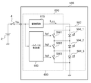
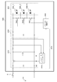
- FIG. 2 is a block diagram of a vehicle lamp 500 including a lighting circuit 600 according to the embodiment.
- the DC voltage (input voltage) VIN from the battery 2 is supplied to the vehicle lamp 500 via the switch 4.
- the vehicle lamp 500 includes a semiconductor light source 502 and a lighting circuit 600.
- the semiconductor light source 502 includes a plurality of n (n ⁇ 2) light emitting elements 504_1, 504_2,... 504_n connected in series.
- the light emitting element 504 is preferably, for example, an LED, but is not limited thereto, and may be an LD (laser diode), an organic EL element, or the like.
- the vehicle lamp 500 is, for example, a headlamp, and the semiconductor light source 502 may be a white LED.
- the lighting circuit 600 includes a drive circuit 610, a plurality of bypass switches SW1 to SW3, and a bypass control unit 650.
- the drive circuit 610 receives the input voltage V IN and supplies the semiconductor light source 502 with a drive current I LED stabilized to the target amount I REF . If the drive circuit 610 is configured by a boost converter, the cost increases. Therefore, the drive circuit 610 includes (i) a constant current linear regulator, (ii) a step-down switching converter with a constant current output, or (iii) a step-down switching with a constant voltage output. It can be constituted by any of a combination of a converter and a constant current circuit. From the viewpoint of cost and power consumption, a step-down switching converter with a constant current output is preferably used.
- Each of the plurality of m bypass switches SW1 to SWm is connected in parallel with a corresponding part of the plurality of light emitting elements 504_1 to 504_n.
- the number n of the light emitting elements 504 is the same as the number m of the bypass switches SW, and one bypass switch SW is associated with one light emitting element 504.
- the m-phase gate pulse signals Sg1 to Sg3 shifted by 120 °) are generated, and the m bypass switches SW1 to SW3 are controlled according to the m-phase gate pulse signals Sg1 to Sg3.
- the gate pulse signal Sg # is high, the corresponding bypass switch SW # is on, and the corresponding light emitting element 504_ # is turned off.
- the frequencies of the gate pulse signals Sg1 to Sg3 are equal, and are defined to be higher than 60 Hz, and preferably about 100 to 400 Hz. Thus, the blinking of the light emitting element 504 cannot be perceived by human eyes.
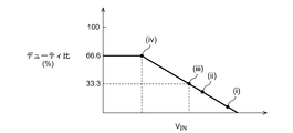
- FIG. 3 is a diagram showing the relationship between the input voltage VIN and the duty ratio of the gate pulse signal in the lighting circuit 600.
- the number k of bypass switches that are turned on at the same time is changed to 0, 1, or 2 according to the decrease in the input voltage VIN .
- the number changes to three, two, or one according to the input voltage VIN .
- the duty ratio of the gate pulse signal Sg increases from 0% to (k MAX ⁇ 100 / m)% as the input voltage VIN decreases.
- k MAX is the maximum number of bypass switches that are turned on at the same time, in other words, the maximum number of light emitting elements 504 that are turned off at the same time.
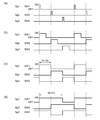
- FIGS. 4A to 4D are operation waveform diagrams of the lighting circuit 600.
- FIGS. 4A to 4D show four states in which the input voltage VIN is different. Each state corresponds to the operating points (i) to (iv) in FIG.
- the lighting circuit 600 the number of light emitting elements 504 to be lighted can be gradually reduced as the input voltage VIN decreases. Furthermore, since the light emitting elements 504 that are turned off are sequentially switched in the cycle of the gate pulse signal Sg, a situation in which the same light emitting element 504 is always turned off can be avoided, and unevenness of the luminance distribution of the semiconductor light source 502 can be eliminated. When the vehicle lamp 500 is a headlamp, unevenness of the light distribution pattern can be reduced.
- FIG. 5 is a diagram showing a relationship between the input voltage VIN and the light amount of the semiconductor light source 502.
- FIG. 5 shows a power supply voltage characteristic of a light amount of a conventional halogen lamp for comparison.
- the characteristics of the illustrated halogen lamp and the present embodiment respectively show relative values of the respective light amounts when the power supply voltage changes, with the light amount when the power supply voltage VIN is 13.5 V as 100%.
- the light emission amount is continuously reduced with the decrease of the input voltage VIN. To decline. This makes it possible to reproduce the characteristics of a halogen lamp in which the amount of light decreases as the power supply voltage decreases.
- chattering luminance of the semiconductor light source 502 changes discontinuously may occur
- the present embodiment also has an advantage that such chattering can be suppressed.
- FIG. 6 is a diagram illustrating another example of the relationship between the input voltage VIN and the duty ratio of the gate pulse signal in the lighting circuit 600.
- k MAX 1, and the number k of bypass switches that are simultaneously turned on is changed to 0 or 1 in accordance with a decrease in the input voltage VIN .
- the number changes to three or two according to the input voltage VIN .
- the present invention extends to various devices and methods grasped as the block diagram and circuit diagram of FIG. 2 or derived from the above description, and is not limited to a specific configuration.
- more specific configuration examples and embodiments will be described, not to narrow the scope of the present invention but to help understand the essence and operation of the present invention and to clarify them.
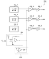
- FIG. 7 is a block diagram illustrating a configuration example of the bypass control unit 650.
- the plurality (m) of ramp generators 652_1 to 652_m generate ramp waves Vramp1 to Vramp3 having a phase difference of 360 ° / m.
- the non-inverting amplifier 654 amplifies the input voltage VIN .
- the clamp circuit 656 clamps the duty ratio command voltage Vcnt of the non-inverting amplifier 654 so as not to fall below a predetermined lower limit voltage Vcl. This lower limit voltage Vcl is determined so that the duty ratio is 66.6%.
- the duty ratios of these pulses are equal and their phases are shifted by 360 ° / m.
- Driver 659_ # outputs gate pulse signal Sg # corresponding to PWM signal Spwm # output from corresponding voltage comparator 658_ #.
- FIG. 8 is an operation waveform diagram of the bypass control unit 650 of FIG. As described above, according to the bypass control unit 650 of FIG. 7, it is possible to generate a plurality of gate pulse signals Sg1 to Sg3 having a duty ratio according to the input voltage VIN and having shifted phases.
- the non-inverting amplifier 654 may be constituted by an inverting amplifier.
- the clamp circuit 656 may limit the duty ratio command voltage Vcnt output from the inverting amplifier so as not to exceed a predetermined upper limit level. The same operation can be realized by exchanging the inverting input and the non-inverting potential of the voltage comparator 658 or configuring the driver 659 with an inverting type.
- FIG. 9 is a block diagram illustrating a configuration example of the drive circuit 610.
- the drive circuit 610 includes a step-down converter (buck converter) 612, a converter controller 614, and a current smoothing filter 616.
- Converter controller 614 controls the switching state of converter controller 614 by feedback so that drive current I LED approaches target amount I REF .
- a current smoothing filter 616 may be connected to the output of 612. Current smoothing filter 616 to remove the ripple of the drive current I LED with the ripple control method, it is possible to suppress the drive current I LED overcurrent due to abrupt load variations.
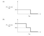
- FIGS. 10A and 10B are diagrams illustrating the relationship between the input voltage VIN and the duty ratio of the gate pulse signal in the lighting circuit 600 according to the first modification.
- bypass control unit 650 determines the number k of the bypass switches SW1 to SW3 to be turned on at the same time according to the input voltage VIN . Then, the bypass control unit 650 switches the k bypass switches that are in the ON state at a predetermined cycle (about 100 to 200 Hz).
- the duty ratio is changed at a constant gradient with respect to the input voltage VIN , but this is not a limitation.
- the duty ratio may change according to a combination of a plurality of linear functions having different gradients, a quadratic function, or another curve, instead of a straight line (linear function) having a constant gradient.
- the phase difference between the m-phase gate pulse signals is set equal to 360 ° / m.
- the present invention is not limited thereto, and the phase difference may not be necessarily uniform.
- Modification 4 In the embodiment, the case where the vehicle lamp 500 is a headlamp has been described. However, the present invention is not limited to this, and the present invention may be applied to a DRL (Daytime Running Lamps) or an amber LED for a turn signal.
- DRL Daytime Running Lamps
- amber LED for a turn signal.
- the vehicular lamp 500 may be a stop lamp or a tail lamp, or may be an LED socket in which the semiconductor light source 502 and the lighting circuit 600 are housed in one package.
- the brightness distribution of the semiconductor light source 502 is made uniform, so that the appearance can be prevented from being impaired.
- a current smoothing filter 616 for suppressing overcurrent or ringing is provided at the output stage of the drive circuit 610. From the viewpoints of mounting area, cost, and the like, there are cases where it is desired to select a component having a small chip size and therefore a small inductance as the inductor of the current smoothing filter 616, or to omit the inductor itself. If the inductance is small (or zero), the charge of the capacitor of the current smoothing filter 616 is discharged due to the fluctuation of the voltage Vout across the semiconductor light source 502 due to the turn-on of the bypass switch, and the discharge current is reduced by the output current of the step-down converter 612. Is superimposed on Thus the overshoot occurs in the drive current I LED supplied to the semiconductor light source 502, or there is a possibility that overcurrent flows.
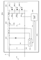
- FIG. 11 is a circuit diagram of a vehicle lamp 500A according to a fifth modification.
- the bypass control unit 650 generates a timing signal St synchronized with turning on of each of the bypass switches SW1 to SW3.
- This timing signal St is supplied to an enable pin (inverted logic) ⁇ EN ( ⁇ represents logical inversion) of the converter controller 614.
- the converter controller 614 fixes the drive signal Sd supplied to the gate of the switching transistor to the off level during the stop period ⁇ , and stops the switching of the step-down converter 612.
- the length of the stop period ⁇ is determined so as to cancel overshoot or overcurrent of the drive current caused by the turn-on of each of the bypass switches SW1 to SW3, as described later.
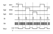
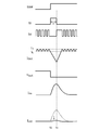
- FIG. 12 is a time chart of the operation of the vehicle lamp 500A of FIG.
- the timing signal St is asserted (high) at the timing when each of the bypass switches SW1 to SW3 is turned off, and then negated (low) after a predetermined time ⁇ has elapsed. While the timing signal St is asserted, the drive signal Sd is fixed at a low level (the off level of the switching transistor), and the switching of the step-down converter 612 stops. While all the bypass switches SW1 to SW3 are off, the voltage Vout between both ends of the load is 3 ⁇ Vf, and while any of the bypass switches is on, the voltage Vout is 2 ⁇ Vf.
- FIG. 13 is an operation waveform diagram of the vehicle lamp 500A of FIG.
- converter controller 614 stabilizes output current Iout of step-down converter 612 by Bang-Bang control.
- Converter controller 614 is specifically a period of the timing signal St negated, the output current Iout to transition off level and the driving signal Sd reaches the peak current I H, and the output current Iout decreases to bottom current I L driven The signal Sd transitions to the on level. Further, the drive signal Sd is fixed at the off level while the timing signal St is asserted.
- the bypass switch SW # When the bypass switch SW # is turned on in a time t 0, the voltage across Vout of the load is reduced. At this time, the capacitor C1 of the current smoothing filter 616 is discharged, and the discharge current Idis is supplied to the semiconductor light source 502. If If the output current Iout of the step-down converter 612 at this time is maintained at a constant level, the load current I LED supplied to the semiconductor light source 502, overshoots as indicated by a chain line.
- the switching operation of the step-down converter 612 is stopped during the stop period ⁇ from time t 0 to t 1 , and the output current Iout is reduced.
- the discharge current Id is the output current Iout is canceled, it is possible to suppress the overshoot of the load current I LED as shown by the solid line.
- the length of the stop period ⁇ may be optimized so that overshoot can be suppressed.
- the inductor of the current smoothing filter 616 can be omitted, or an inexpensive and / or small inductor having a small inductance value can be used.
- FIG. 11 shows a diode rectification type converter, but this modification is also effective for a synchronous rectification type converter as shown in FIG.
- the Bang-Bang control is described here as an example, another ripple control method such as a peak detection off time fixed mode or a bottom detection on time fixed mode may be adopted. Alternatively, a control method using an error amplifier may be used.
- the timing signal St is input to the EN pin of the converter controller 614;
- the timing signal St may be a signal indicating the start timing of the stop period ⁇ , and the converter controller 614 specifies the driving of the step-down converter 612 in response to the assertion of the timing signal St, and the stop timer ⁇ is set by an internal timer. May be measured, and the drive of the step-down converter 612 may be restarted after the stop period ⁇ has elapsed.
- the present invention relates to a lamp used for an automobile or the like.
Landscapes
- Physics & Mathematics (AREA)
- Electromagnetism (AREA)
- Circuit Arrangement For Electric Light Sources In General (AREA)
- Lighting Device Outwards From Vehicle And Optical Signal (AREA)
Abstract
駆動回路(610)は、入力電圧(VIN)を受け、半導体光源(502)に駆動電流(ILED)を供給する。複数m個(m≧2)のバイパススイッチ(SW1~SW3)は、複数の発光素子(504_1~504_3)と並列に接続される。バイパス制御部(650)は、入力電圧(VIN)に応じたデューティ比を有し、位相が360°/mずつシフトしているm相のゲートパルス信号(Sg1~Sg3)を生成し、m相のゲートパルス信号に応じてm個のバイパススイッチ(SW1~SW3)を制御する。
Description
本発明は、自動車などに用いられる灯具に関する。
車両用灯具に用いられる光源として、従来は電球が多く用いられてきたが、近年では、LED(発光ダイオード)などの半導体光源が広く採用されるようになっている。
図1は、従来の車両用灯具1のブロック図である。車両用灯具1には、スイッチ4を介してバッテリ2からの直流電圧(入力電圧VIN)を受ける。光源10は、直列に接続される複数n個のLED12を含む。光源10の輝度は、それに流れる駆動電流ILEDに応じて制御される。点灯回路20は、駆動電流ILEDを目標輝度に応じた目標量IREFに安定化するLEDドライバ22を含む。
LED12に、目標量IREFに安定化された駆動電流ILEDが流れているときの順方向電圧をVf0とすると、光源10の両端間電圧(最低点灯電圧という)VMINは、Vf0×nとなる。n=3とすると、白色LEDではVMIN≒11Vであり、赤色LEDではVMIN≒9Vである。言い換えると、LEDドライバ22の出力電圧VOUTが、この最低点灯電圧VMINを下回ると、駆動電流ILEDが目標量IREFを維持できなくなり、複数のLED12が消灯する。
低コスト化が求められる点灯回路20では、LEDドライバ22は、定電流シリーズレギュレータあるいは定電流出力のスイッチングコンバータで構成される。この場合、LEDドライバ22の出力電圧VOUTは、入力電圧VINより低くなる。入力電圧VINは、バッテリの満充電状態で13Vであるが、放電が進むと、10V以下まで低下することも珍しくない。したがって、バッテリ電圧が低下すると(低電圧状態という)、出力電圧VOUTが最低点灯電圧VMINを下回る状況が生じ、LED12が消灯する。
低電圧状態における光源10の消灯を防止するためにバイパススイッチ24およびバイパス制御回路26が設けられる。バイパススイッチ24は、1個のLED12_nと並列に接続される。バイパス制御回路26は、入力電圧VINがあるしきい値VTHより低くなると低電圧状態と判定し、バイパススイッチ24をオンする。この状態では、最低点灯電圧VMIN=Vf0×(n-1)となり、VIN>VMINが保たれる。つまり、LED12_nの消灯と引き換えに、残りのLED12_1~12_(n-1)の点灯を維持することができる。
本発明者らは図1の点灯回路20について検討した結果、以下の課題を認識するに至った。
図1の点灯回路20では、低電圧状態において常に同じLED12_nが消灯する。通常、複数のLED12_1~12_nは、同一平面上に並べて配置されるため、同じLED12_nが常に消灯していると、そのLED12_nに対応する箇所だけが暗くなる。車両用灯具1が前照灯である場合、配光パターンにむらが現れ、運転者が車両前方を見にくくなるおそれがある。また車両用灯具1がストップランプやテールランプである場合、美観を損ねるおそれがある。
本発明はかかる課題に鑑みてなされたものであり、そのある態様の例示的な目的のひとつは、低電圧状態における半導体光源の輝度ムラを抑制可能な点灯回路の提供にある。
本発明のある態様は、直列に接続される複数の発光素子を含む半導体光源のための点灯回路に関する。点灯回路は、入力電圧を受け、半導体光源に駆動電流を供給する駆動回路と、それぞれが複数の発光素子の対応する一部と並列に接続される複数m個(m≧2)のバイパススイッチと、入力電圧に応じたデューティ比を有し、位相シフトしているm相のゲートパルス信号を生成し、m相のゲートパルス信号に応じてm個のバイパススイッチを制御するバイパス制御部と、を備える。
本発明の別の態様もまた、点灯回路である。この点灯回路は、入力電圧を受け、半導体光源に駆動電流を供給する駆動回路と、それぞれが複数の発光素子の対応する一部と並列に接続される複数m個(m≧2)のバイパススイッチと、入力電圧に応じて、同時にオン状態とすべきバイパススイッチの個数kを決定し、オン状態のバイパススイッチを所定の周期で変化させるバイパス制御部と、を備える。
なお、以上の構成要素の任意の組み合わせや本発明の構成要素や表現を、方法、装置、システムなどの間で相互に置換したものもまた、本発明の態様として有効である。
本発明のある態様によれば、半導体光源の輝度ムラを抑制できる。
本明細書に開示される一実施の形態は、直列に接続される複数の発光素子を含む半導体光源のための点灯回路に関する。点灯回路は、入力電圧を受け、半導体光源に駆動電流を供給する駆動回路と、それぞれが複数の発光素子の対応する一部と並列に接続される複数m個(m≧2)のバイパススイッチと、入力電圧に応じたデューティ比を有し、位相が360°/mずつシフトしているm相のゲートパルス信号を生成し、m相のゲートパルス信号に応じてm個のバイパススイッチを制御するバイパス制御部と、を備える。
デューティ比が角度換算で360°/mとなると、常に1個のバイパススイッチがオン状態となり、発光素子の一部が消灯した状態となる。そしてオン状態となるバイパススイッチは順に入れ替わるため、消灯する発光素子も順に入れ替わり、半導体光源の輝度ムラを抑制できる。
m相のゲートパルス信号のデューティ比は、入力信号に応じて連続的に変化してもよい。これにより、入力電圧の低下にともなって、半導体光源の光量を連続的に低下させることができ、ハロゲンランプのような自然な減光な電源電圧特性を再現できる。また、デューティ比を不連続に変化させると、あるしきい値近傍で入力電圧が変動するときに、半導体光源の輝度が不連続に変化するチャタリングが発生しうるが、デューティ比を連続的に変化させることで、チャタリングを抑制できる。
駆動回路は、降圧コンバータと、駆動電流が目標量に近づくように降圧コンバータをフィードバック制御するコンバータコントローラと、を含んでもよい。負荷変動に対する追従性の高いリップル制御方式を採用してもよい。これによりバイパススイッチのターンオンに起因する駆動電流の増大を抑制できる。
駆動回路は、降圧コンバータの出力と接続される電流平滑化フィルタをさらに含んでもよい。電流平滑化フィルタによって、負荷変動に起因する駆動電流の変動を抑制できる。
コンバータコントローラは、バイパススイッチのターンオンと同期したスタートタイミングから停止期間の間、降圧コンバータの駆動を停止してもよい。電流平滑化フィルタの放電電流と、降圧コンバータの出力電流の減少が相殺することにより、オーバーシュートや過電流を抑制できる。
(実施の形態)
以下、本発明を好適な実施の形態をもとに図面を参照しながら説明する。各図面に示される同一または同等の構成要素、部材、処理には、同一の符号を付するものとし、適宜重複した説明は省略する。また、実施の形態は、発明を限定するものではなく例示であって、実施の形態に記述されるすべての特徴やその組み合わせは、必ずしも発明の本質的なものであるとは限らない。
以下、本発明を好適な実施の形態をもとに図面を参照しながら説明する。各図面に示される同一または同等の構成要素、部材、処理には、同一の符号を付するものとし、適宜重複した説明は省略する。また、実施の形態は、発明を限定するものではなく例示であって、実施の形態に記述されるすべての特徴やその組み合わせは、必ずしも発明の本質的なものであるとは限らない。
本明細書において、「部材Aが、部材Bと接続された状態」とは、部材Aと部材Bが物理的に直接的に接続される場合のほか、部材Aと部材Bが、それらの電気的な接続状態に実質的な影響を及ぼさない、あるいはそれらの結合により奏される機能や効果を損なわせない、その他の部材を介して間接的に接続される場合も含む。
同様に、「部材Cが、部材Aと部材Bの間に設けられた状態」とは、部材Aと部材C、あるいは部材Bと部材Cが直接的に接続される場合のほか、それらの電気的な接続状態に実質的な影響を及ぼさない、あるいはそれらの結合により奏される機能や効果を損なわせない、その他の部材を介して間接的に接続される場合も含む。
また本明細書において、電圧信号、電流信号などの電気信号、あるいは抵抗、キャパシタなどの回路素子に付された符号は、必要に応じてそれぞれの電圧値、電流値、あるいは抵抗値、容量値を表すものとする。
図2は、実施の形態に係る点灯回路600を備える車両用灯具500のブロック図である。車両用灯具500には、スイッチ4を介してバッテリ2からの直流電圧(入力電圧)VINが供給される。車両用灯具500は、半導体光源502および点灯回路600を備える。半導体光源502は、直列に接続される複数n個(n≧2)の発光素子504_1,504_2,…504_nを含む。図2にはn=3の場合が示される。発光素子504はたとえばLEDが好適であるが、その限りでなく、LD(レーザダイオード)や有機EL素子などを採用してもよい。車両用灯具500は、たとえばヘッドランプであり、半導体光源502は白色LEDであってもよい。
点灯回路600は、駆動回路610、複数のバイパススイッチSW1~SW3、バイパス制御部650を備える。
駆動回路610は入力電圧VINを受け、半導体光源502に目標量IREFに安定化された駆動電流ILEDを供給する。駆動回路610を昇圧コンバータで構成するとコストが高くなることから、駆動回路610は、(i)定電流リニアレギュレータ、(ii)定電流出力の降圧スイッチングコンバータあるいは、(iii)定電圧出力の降圧スイッチングコンバータと定電流回路の組み合わせ、のいずれかで構成することができる。コストと消費電力の観点からは、定電流出力の降圧スイッチングコンバータを用いるとよい。
複数m個のバイパススイッチSW1~SWmはそれぞれ、複数の発光素子504_1~504_nの対応する一部と並列に接続される。本実施の形態では、発光素子504の個数nはバイパススイッチSWの個数mと同じであり、1個のバイパススイッチSWは、1個の発光素子504に対応付けられる。バイパススイッチSWi(i=1,2,3)がオン状態となると、駆動電流ILEDはバイパススイッチSWi側に引き込まれ、対応する発光素子504_iは消灯する。
バイパス制御部650は、入力電圧VINに応じたデューティ比、より正確には入力電圧VINと負の相関を有するデューティ比を有し、位相が(360/m)°(m=3のとき120°)ずつシフトしているm相のゲートパルス信号Sg1~Sg3を生成し、m相のゲートパルス信号Sg1~Sg3に応じてm個のバイパススイッチSW1~SW3を制御する。本実施の形態ではゲートパルス信号Sg#がハイのときに、対応するバイパススイッチSW#はオンであり、対応する発光素子504_#は消灯する。ゲートパルス信号Sg1~Sg3の周波数は等しく、60Hzより高く規定され、好ましくは100~400Hz程度としてもよい。これにより、発光素子504の点滅は人間の目によって知覚できなくなる。
以上が点灯回路600の基本的な構成である。続いてその動作を説明する。図3は、点灯回路600における入力電圧VINとゲートパルス信号のデューティ比の関係を示す図である。本実施の形態では、同時にオン状態となるバイパススイッチの個数kを、入力電圧VINの低下に応じて、0個、1個、2個と変化させるものとし、したがって同時点灯する発光素子504の個数は、入力電圧VINに応じて、3個、2個、1個と変化する。
ゲートパルス信号Sgのデューティ比は、入力電圧VINの低下とともに、0%から、(kMAX×100/m)%まで増大する。kMAXは同時にオン状態となるバイパススイッチの最大個数、言い換えれば同時に消灯する発光素子504の最大個数である。m=3、kMAX=2のとき、デューティ比は0%から66%の範囲で変化する。
図4(a)~(d)は、点灯回路600の動作波形図である。図4(a)~(d)は、入力電圧VINが異なる4つの状態を示している。各状態は、図3の動作点(i)~(iv)に対応する。
以上が点灯回路600および車両用灯具500の動作である。この点灯回路600によれば、入力電圧VINの低下にともない、点灯する発光素子504の個数を徐々に減らすことができる。さらに消灯している発光素子504が、ゲートパルス信号Sgの周期で順に入れ替わるため、常に同じ発光素子504が消灯する状況を回避でき、半導体光源502の輝度分布のムラを解消できる。車両用灯具500がヘッドランプである場合、配光パターンのムラを低減できる。
車両用灯具500のさらなる利点を説明する。図5は、入力電圧VINと半導体光源502の光量の関係を示す図である。図5には、比較のために、従来のハロゲンランプの光量の電源電圧特性が示される。図示されるハロゲンランプおよび本実施の形態の特性はそれぞれ、電源電圧VINが13.5Vのときの光量を100%として、電源電圧が変化したときの各光量の相対値を示す。2本の特性の比較からわかるように、入力電圧VINに応じて、デューティ比を徐々に変化させることにより、図5に示すように、発光量は入力電圧VINの低下にともない、連続的に低下していく。これにより、電源電圧の低下にともなって光量が低下するハロゲンランプの特性を再現できる。
入力電圧VINに対して、デューティ比を不連続に変化させると、不連続点の近傍で入力電圧VINが変動したときに、半導体光源502の輝度が不連続に変化するチャタリングが発生しうるが、本実施の形態では、このようなチャタリングを抑制できるという利点もある。
図6は、点灯回路600における入力電圧VINとゲートパルス信号のデューティ比の関係の別の一例を示す図である。この例ではkMAX=1であり、同時にオン状態となるバイパススイッチの個数kを、入力電圧VINの低下に応じて0個、1個と変化させるものとし、したがって同時点灯する発光素子504の個数は、入力電圧VINに応じて、3個、2個と変化する。ゲートパルス信号Sgのデューティ比は、入力電圧VINの低下とともに、0%から33%(=kMAX×100/m)まで増大する。
本発明は、図2のブロック図や回路図として把握され、あるいは上述の説明から導かれるさまざまな装置、方法に及ぶものであり、特定の構成に限定されるものではない。以下、本発明の範囲を狭めるためではなく、発明の本質や動作の理解を助け、またそれらを明確化するために、より具体的な構成例や実施例を説明する。
図7は、バイパス制御部650の構成例を示すブロック図である。複数(m個)のランプ波発生器652_1~652_mは、位相差が360°/mであるランプ波Vramp1~Vramp3を生成する。
非反転アンプ654は、入力電圧VINを増幅する。クランプ回路656は、非反転アンプ654のデューティ比指令電圧Vcntを、所定の下限電圧Vclを下回らないようにクランプする。この下限電圧Vclは、デューティ比が66.6%となるように定められる。
電圧コンパレータ658_#(#=1,2,3)は、デューティ比指令電圧Vcntと対応するランプ波Vramp#を比較し、矩形のパルス(PWM信号)Spwm#を出力する。これらのパルスのデューティ比は等しく、それらの位相は360°/mずつシフトしている。
ドライバ659_#は、対応する電圧コンパレータ658_#から出力されるPWM信号Spwm#に応じたゲートパルス信号Sg#を出力する。
図8は、図7のバイパス制御部650の動作波形図である。このように図7のバイパス制御部650によれば、入力電圧VINに応じたデューティ比を有し、位相がシフトした複数のゲートパルス信号Sg1~Sg3を生成できる。
なお図7において、非反転アンプ654を反転アンプで構成してもよい。クランプ回路656は、反転アンプの出力であるデューティ比指令電圧Vcntを、所定の上限レベルを超えないように制限してもよい。そして、電圧コンパレータ658の反転入力と非反転有力を入れ替えるか、あるいはドライバ659を反転型で構成することで、同じ動作を実現できる。
図9は、駆動回路610の構成例を示すブロック図である。駆動回路610は、降圧コンバータ(Buckコンバータ)612と、コンバータコントローラ614、電流平滑化フィルタ616を備える。コンバータコントローラ614は、駆動電流ILEDが目標量IREFに近づくように、フィードバックによりコンバータコントローラ614のスイッチング状態を制御する。
図4(a)や(b)に示す動作モードでは、すべてのバイパススイッチがオフの状態とが1個のバイパススイッチのみがオンの状態と、が交互に現れる。すべてのバイパススイッチがオフであるとき、半導体光源502の両端間電圧の電圧(すなわち降圧コンバータ612の出力電圧)は3×Vf0であり、1個のバイパススイッチがオンの状態では、半導体光源502の両端間電圧は2×Vf0となり、不連続に変動する。このような不連続かつ急峻な負荷変動は、駆動電流ILEDの過電流状態(あるいはリンギング)を引き起こすおそれがある。そこで急峻な負荷変動に追従するために、高速応答性に優れるリップル制御方式のコンバータコントローラ614を採用するとよい。リップル制御方式は、ヒステリシス制御(Bang-Bang制御)、ボトム検出オン時間固定制御、ピーク検出オフ時間固定制御などが例示される。
なお、コンバータコントローラ614にリップル制御方式でなく、エラーアンプを用いたフィードバック回路を採用する場合、あるいはリップル制御方式を採用したとしても、駆動電流ILEDに過電流が生ずるおそれがあるため、降圧コンバータ612の出力に、電流平滑化フィルタ616を接続してもよい。電流平滑化フィルタ616は、リップル制御方式にともなう駆動電流ILEDのリップルを除去するとともに、急峻な負荷変動にともなう駆動電流ILEDの過電流を抑制できる。
以上、本発明について、実施の形態をもとに説明した。この実施の形態は例示であり、それらの各構成要素や各処理プロセスの組み合わせにいろいろな変形例が可能なこと、またそうした変形例も本発明の範囲にあることは当業者に理解されるところである。以下、こうした変形例について説明する。
(変形例1)
実施の形態では、ゲートパルスSgのデューティ比を、入力電圧VINに応じて連続的に変化させたがその限りでない。図10(a)、(b)は、変形例1に係る点灯回路600における入力電圧VINとゲートパルス信号のデューティ比の関係を示す図である。図10(a)はm=3、kMAX=1の場合、図10(b)はm=3、kMAX=2の場合である。この変形例によっても、入力電圧VINが低下した状態において、特定の発光素子504が固定的にオフとなるのを防止でき、半導体光源502の輝度ムラを抑制できる。
実施の形態では、ゲートパルスSgのデューティ比を、入力電圧VINに応じて連続的に変化させたがその限りでない。図10(a)、(b)は、変形例1に係る点灯回路600における入力電圧VINとゲートパルス信号のデューティ比の関係を示す図である。図10(a)はm=3、kMAX=1の場合、図10(b)はm=3、kMAX=2の場合である。この変形例によっても、入力電圧VINが低下した状態において、特定の発光素子504が固定的にオフとなるのを防止でき、半導体光源502の輝度ムラを抑制できる。
なお、この変形例におけるバイパス制御部650の機能は、以下のように把握できる。すなわちバイパス制御部650は、入力電圧VINに応じて、同時にオン状態とすべきバイパススイッチSW1~SW3の個数kを決定する。そしてバイパス制御部650は、所定の周期(100~200Hz程度)で、オン状態であるk個のバイパススイッチを入れ替える。
(変形例2)
図3や図6においてデューティ比を入力電圧VINに対して一定の傾きで変化させたがその限りでない。たとえばデューティ比0%と33%の途中、あるいは33%と66%mの途中に、デューティ比が入力電圧に依存しない平坦な部分があってもよい。あるいは、一定の傾きの直線(1次関数)でなく、傾きが異なる複数の1次関数の組み合わせ、あるいは2次関数やその他の曲線にしたがってデューティ比が変化してもよい。
図3や図6においてデューティ比を入力電圧VINに対して一定の傾きで変化させたがその限りでない。たとえばデューティ比0%と33%の途中、あるいは33%と66%mの途中に、デューティ比が入力電圧に依存しない平坦な部分があってもよい。あるいは、一定の傾きの直線(1次関数)でなく、傾きが異なる複数の1次関数の組み合わせ、あるいは2次関数やその他の曲線にしたがってデューティ比が変化してもよい。
(変形例3)
実施の形態では、m相のゲートパルス信号の位相差を等しく360°/mとしたがその限りでなく、位相差は必ずしも均一でなくてもよい。
実施の形態では、m相のゲートパルス信号の位相差を等しく360°/mとしたがその限りでなく、位相差は必ずしも均一でなくてもよい。
(変形例4)
実施の形態では、車両用灯具500がヘッドランプである場合を説明したが、その限りでなく、DRL(Daytime Running Lamps)であってもよいし、ターンシグナル用のアンバーLEDにも適用できる。
実施の形態では、車両用灯具500がヘッドランプである場合を説明したが、その限りでなく、DRL(Daytime Running Lamps)であってもよいし、ターンシグナル用のアンバーLEDにも適用できる。
あるいは車両用灯具500は、ストップランプやテールランプであってもよく、半導体光源502と点灯回路600とが1パッケージに収容されたLEDソケットであってもよい。この場合、低電圧状態において、半導体光源502の輝度分布が均一化されることにより、美観が損なわれるのを防止できる。
(変形例5)
図9の車両用灯具500では、駆動回路610の出力段に、過電流あるいはリンギングを抑制するための電流平滑化フィルタ616が設けられている。実装面積やコストなどの都合から、電流平滑化フィルタ616のインダクタとして、チップサイズの小さい、したがってインダクタンスの小さい部品を選択し、あるいはインダクタ自体を省略したい場合がある。インダクタンスが小さい(あるいはゼロである)と、バイパススイッチのターンオンにともなう半導体光源502の両端間電圧Voutの変動によって電流平滑化フィルタ616のキャパシタから電荷が放電され、放電電流が降圧コンバータ612の出力電流に重畳される。これにより半導体光源502に供給される駆動電流ILEDにオーバーシュートが発生し、あるいは過電流が流れるおそれがある。
図9の車両用灯具500では、駆動回路610の出力段に、過電流あるいはリンギングを抑制するための電流平滑化フィルタ616が設けられている。実装面積やコストなどの都合から、電流平滑化フィルタ616のインダクタとして、チップサイズの小さい、したがってインダクタンスの小さい部品を選択し、あるいはインダクタ自体を省略したい場合がある。インダクタンスが小さい(あるいはゼロである)と、バイパススイッチのターンオンにともなう半導体光源502の両端間電圧Voutの変動によって電流平滑化フィルタ616のキャパシタから電荷が放電され、放電電流が降圧コンバータ612の出力電流に重畳される。これにより半導体光源502に供給される駆動電流ILEDにオーバーシュートが発生し、あるいは過電流が流れるおそれがある。
図11は、変形例5に係る車両用灯具500Aの回路図である。バイパス制御部650は、バイパススイッチSW1~SW3それぞれがターンオンと同期したタイミング信号Stを発生する。このタイミング信号Stは、コンバータコントローラ614のイネーブルピン(反転論理)\EN(\は論理反転を表す)に供給される。コンバータコントローラ614は、タイミング信号Stにもとづいて、停止期間τの間、スイッチングトランジスタのゲートに供給する駆動信号Sdをオフレベルに固定し、降圧コンバータ612のスイッチングを停止する。停止期間τの長さは、後述のように、バイパススイッチSW1~SW3それぞれのターンオンに起因する駆動電流のオーバーシュートや過電流をキャンセルできるように定められる。
続いて車両用灯具500の動作を、図12,図13を参照して説明する。図12は、図11の車両用灯具500Aの動作のタイムチャートである。タイミング信号Stは、バイパススイッチSW1~SW3それぞれがターンオフするタイミングでアサート(ハイ)され、それから所定時間τの経過後にネゲート(ロー)される。タイミング信号Stがアサートの期間、駆動信号Sdがロー(スイッチングトランジスタのオフレベル)に固定され、降圧コンバータ612のスイッチングが停止する。すべてバイパススイッチSW1~SW3がオフの間、負荷の両端間の電圧Voutは3×Vf、いずれかのバイパススイッチがオンの間、電圧Voutは2×Vfである。
図13は、図11の車両用灯具500Aの動作波形図である。この例では、コンバータコントローラ614は、Bang-Bang制御によって降圧コンバータ612の出力電流Ioutを安定化している。具体的にはコンバータコントローラ614は、タイミング信号Stがネゲートの期間、出力電流Ioutがピーク電流IHに達すると駆動信号Sdをオフレベルに遷移させ、出力電流Ioutがボトム電流ILまで低下すると駆動信号Sdをオンレベルに遷移させる。またタイミング信号Stがアサートの期間、駆動信号Sdをオフレベルに固定する。
時刻t0にあるバイパススイッチSW#がターンオンすると、負荷の両端間電圧Voutが低下する。このとき、電流平滑化フィルタ616のキャパシタC1が放電され、放電電流Idisが半導体光源502に供給される。もしこのとき降圧コンバータ612の出力電流Ioutが一定レベルに維持されていれば、半導体光源502に供給される負荷電流ILEDは、一点鎖線で示すようにオーバーシュートする。
これに対して本変形例では、時刻t0~t1の停止期間τの間、降圧コンバータ612のスイッチング動作が停止し、その出力電流Ioutが減少する。出力電流Ioutの減少と放電電流Idisが相殺することにより、実線で示すように負荷電流ILEDのオーバーシュートを抑制することができる。停止期間τの長さは、オーバーシュートを抑制できるように最適化すればよい。この変形例によれば、電流平滑化フィルタ616のインダクタを省略することができ、あるいはインダクタンス値の小さい安価および/または小型のインダクタを用いることができる。
なお図11はダイオード整流型のコンバータを示すが、図9のように同期整流型のコンバータにもこの変形は有効である。またここではBang-Bang制御を例としたが、ピーク検出オフ時間固定モードや、ボトム検出オン時間固定モードなど、別のリップル制御方式を採用してもよい。あるいは、エラーアンプを用いた制御方式を用いてもよい。
図11では、コンバータコントローラ614のENピンに、タイミング信号Stを入力したがその限りでない。タイミング信号Stは、停止期間τの開始タイミングを示す信号であってもよく、コンバータコントローラ614は、タイミング信号Stのアサートに応答して降圧コンバータ612の駆動を指定し、内部のタイマーで停止期間τを測定し、停止期間τの経過後に、降圧コンバータ612の駆動を再開してもよい。
実施の形態にもとづき、具体的な語句を用いて本発明を説明したが、実施の形態は、本発明の原理、応用を示しているにすぎず、実施の形態には、請求の範囲に規定された本発明の思想を逸脱しない範囲において、多くの変形例や配置の変更が認められる。
本発明は、自動車などに用いられる灯具に関する。
2 バッテリ
4 スイッチ
500 車両用灯具
502 半導体光源
504 発光素子
505 被バイパス素子
600 点灯回路
610 駆動回路
612 降圧コンバータ
614 コンバータコントローラ
616 電流平滑化フィルタ
650 バイパス制御部
652 ランプ波発生器
654 反転アンプ
656 クランプ回路
658 電圧コンパレータ
659 ドライバ
4 スイッチ
500 車両用灯具
502 半導体光源
504 発光素子
505 被バイパス素子
600 点灯回路
610 駆動回路
612 降圧コンバータ
614 コンバータコントローラ
616 電流平滑化フィルタ
650 バイパス制御部
652 ランプ波発生器
654 反転アンプ
656 クランプ回路
658 電圧コンパレータ
659 ドライバ
Claims (8)
- 直列に接続される複数の発光素子を含む半導体光源のための点灯回路であって、
入力電圧を受け、前記半導体光源に駆動電流を供給する駆動回路と、
それぞれが前記複数の発光素子の対応する一部と並列に接続される複数m個(m≧2)のバイパススイッチと、
前記入力電圧に応じたデューティ比を有し、位相シフトしているm相のゲートパルス信号を生成し、前記m相のゲートパルス信号に応じて前記m個のバイパススイッチを制御するバイパス制御部と、
を備えることを特徴とする点灯回路。 - 前記m相のゲートパルス信号のデューティ比は、前記入力電圧に応じて連続的に変化することを特徴とする請求項1に記載の点灯回路。
- 直列に接続される複数の発光素子を含む半導体光源のための点灯回路であって、
入力電圧を受け、前記半導体光源に駆動電流を供給する駆動回路と、
それぞれが前記複数の発光素子の対応する一部と並列に接続され、オン状態において前記駆動電流を迂回させる複数m個(m≧2)のバイパススイッチと、
前記入力電圧に応じて、同時にオン状態とすべきバイパススイッチの個数kを決定し、所定の周期毎に、オン状態であるk個のバイパススイッチを変化させるバイパス制御部と、
を備えることを特徴とする点灯回路。 - 前記駆動回路は、
降圧コンバータと、
前記駆動電流が目標量に近づくように前記降圧コンバータをフィードバック制御するコンバータコントローラと、
を含むことを特徴とする請求項1から3のいずれかに記載の点灯回路。 - 前記駆動回路は、前記降圧コンバータの出力と接続される電流平滑化フィルタをさらに含むことを特徴とする請求項4に記載の点灯回路。
- 前記コンバータコントローラは、前記バイパススイッチのターンオンと同期したスタートタイミングから停止期間の間、前記降圧コンバータの駆動を停止することを特徴とする請求項5に記載の点灯回路。
- 前記コンバータコントローラはリップル制御方式であることを特徴とする請求項4から6のいずれかに記載の点灯回路。
- 複数の発光素子を含む半導体光源と、
前記半導体光源を駆動する請求項1から7のいずれかに記載の点灯回路と、
を備えることを特徴とする車両用灯具。
Priority Applications (4)
| Application Number | Priority Date | Filing Date | Title |
|---|---|---|---|
| JP2020535928A JP7271554B2 (ja) | 2018-08-10 | 2019-08-09 | 点灯回路および車両用灯具 |
| EP19847226.8A EP3836756A4 (en) | 2018-08-10 | 2019-08-09 | LIGHTING CIRCUIT AND VEHICLE LIGHT |
| CN201980053764.8A CN112602378B (zh) | 2018-08-10 | 2019-08-09 | 点亮电路及车辆用灯具 |
| US17/168,275 US20210160989A1 (en) | 2018-08-10 | 2021-02-05 | Lighting circuit |
Applications Claiming Priority (4)
| Application Number | Priority Date | Filing Date | Title |
|---|---|---|---|
| JP2018151992 | 2018-08-10 | ||
| JP2018-151992 | 2018-08-10 | ||
| JP2018-210026 | 2018-11-07 | ||
| JP2018210026 | 2018-11-07 |
Related Child Applications (1)
| Application Number | Title | Priority Date | Filing Date |
|---|---|---|---|
| US17/168,275 Continuation US20210160989A1 (en) | 2018-08-10 | 2021-02-05 | Lighting circuit |
Publications (1)
| Publication Number | Publication Date |
|---|---|
| WO2020032269A1 true WO2020032269A1 (ja) | 2020-02-13 |
Family
ID=69414296
Family Applications (1)
| Application Number | Title | Priority Date | Filing Date |
|---|---|---|---|
| PCT/JP2019/031710 Ceased WO2020032269A1 (ja) | 2018-08-10 | 2019-08-09 | 点灯回路および車両用灯具 |
Country Status (5)
| Country | Link |
|---|---|
| US (1) | US20210160989A1 (ja) |
| EP (1) | EP3836756A4 (ja) |
| JP (1) | JP7271554B2 (ja) |
| CN (1) | CN112602378B (ja) |
| WO (1) | WO2020032269A1 (ja) |
Cited By (3)
| Publication number | Priority date | Publication date | Assignee | Title |
|---|---|---|---|---|
| WO2021213444A1 (en) * | 2020-04-24 | 2021-10-28 | Versitech Limited | Dimming method and circuit for light-emitting-diode (led) systems driven by passive led drivers |
| CN116472198A (zh) * | 2020-11-09 | 2023-07-21 | 罗姆股份有限公司 | 用于驱动发光元件的半导体集成电路、发光元件驱动装置、发光装置及车辆 |
| JP2023554133A (ja) * | 2020-12-21 | 2023-12-26 | ヴァレオ ビジョン | 様々な電力要件を有する照明機能に電力を供給するための照明アセンブリ |
Families Citing this family (3)
| Publication number | Priority date | Publication date | Assignee | Title |
|---|---|---|---|---|
| US12267925B2 (en) * | 2022-11-08 | 2025-04-01 | UnitX, Inc. | Multi-channel LED current control circuit |
| WO2025054264A1 (en) * | 2023-09-05 | 2025-03-13 | Lumileds Llc | Light emitting diode retrofit with dynamic sequential illumination of individual light emitting diode chips |
| DE102023212097B3 (de) * | 2023-12-01 | 2024-11-21 | Continental Automotive Technologies GmbH | Treiberschaltung zur Versorgung einer LED-Anordnung mit einem Konstantstrom |
Citations (2)
| Publication number | Priority date | Publication date | Assignee | Title |
|---|---|---|---|---|
| JP2016197711A (ja) | 2015-04-06 | 2016-11-24 | 株式会社小糸製作所 | 駆動回路、車両用灯具 |
| JP2016225208A (ja) * | 2015-06-02 | 2016-12-28 | ローム株式会社 | 発光素子駆動装置、スイッチ駆動装置 |
Family Cites Families (19)
| Publication number | Priority date | Publication date | Assignee | Title |
|---|---|---|---|---|
| JPH0624430B2 (ja) * | 1988-09-14 | 1994-03-30 | 住友金属工業株式会社 | Dc−dcコンバータ |
| JP3480120B2 (ja) * | 1995-05-26 | 2003-12-15 | 松下電工株式会社 | 放電灯点灯装置 |
| JP4710842B2 (ja) * | 2006-03-31 | 2011-06-29 | ウシオ電機株式会社 | 希ガス蛍光ランプ点灯装置 |
| DE602007007804D1 (de) * | 2006-11-10 | 2010-08-26 | Philips Solid State Lighting | Verfahren und vorrichtung zur steuerung von hintereinandergeschalteten led |
| JP4776596B2 (ja) * | 2007-08-01 | 2011-09-21 | 株式会社小糸製作所 | 車両用灯具の点灯制御装置 |
| KR20110114075A (ko) * | 2010-04-12 | 2011-10-19 | 삼성전자주식회사 | 백라이트 유닛 및 이를 포함한 디스플레이 장치 |
| JP5576818B2 (ja) * | 2011-03-22 | 2014-08-20 | パナソニック株式会社 | 点灯装置及びそれを用いた照明器具 |
| US9265109B2 (en) * | 2012-05-18 | 2016-02-16 | Koito Manufacturing Co., Ltd. | Light source control device |
| JP6030922B2 (ja) * | 2012-06-11 | 2016-11-24 | 株式会社小糸製作所 | 光源制御装置 |
| JP2013258003A (ja) * | 2012-06-12 | 2013-12-26 | Koito Mfg Co Ltd | 半導体光源制御装置 |
| JP6134185B2 (ja) * | 2013-03-29 | 2017-05-24 | 株式会社小糸製作所 | 半導体光源制御装置 |
| JP2014232621A (ja) * | 2013-05-29 | 2014-12-11 | 株式会社小糸製作所 | 光源制御装置 |
| JP6283542B2 (ja) * | 2014-03-14 | 2018-02-21 | 株式会社小糸製作所 | 車両用灯具およびその駆動装置 |
| JP6418443B2 (ja) * | 2014-09-10 | 2018-11-07 | パナソニックIpマネジメント株式会社 | 点灯装置、照明装置および車両 |
| AT516294B8 (de) * | 2014-09-22 | 2017-02-15 | Zkw Group Gmbh | Verfahren und Schaltungsanordnung zum Speisen einer Serienschaltung von n LED-Einheiten |
| JP6396160B2 (ja) * | 2014-10-02 | 2018-09-26 | 株式会社小糸製作所 | 車両用灯具およびその点灯回路 |
| CN108141135B (zh) * | 2015-06-05 | 2020-12-08 | 朝阳半导体技术江阴有限公司 | 电压调节器电流负载感测 |
| EP3244697B1 (en) * | 2016-05-13 | 2020-07-29 | Rohm Co., Ltd. | A method and apparatus for reducing flickering of emitted light |
| US9763296B1 (en) * | 2016-06-15 | 2017-09-12 | Infineon Technologies Ag | Multifunction DC to DC driver |
-
2019
- 2019-08-09 WO PCT/JP2019/031710 patent/WO2020032269A1/ja not_active Ceased
- 2019-08-09 JP JP2020535928A patent/JP7271554B2/ja active Active
- 2019-08-09 CN CN201980053764.8A patent/CN112602378B/zh active Active
- 2019-08-09 EP EP19847226.8A patent/EP3836756A4/en not_active Withdrawn
-
2021
- 2021-02-05 US US17/168,275 patent/US20210160989A1/en not_active Abandoned
Patent Citations (2)
| Publication number | Priority date | Publication date | Assignee | Title |
|---|---|---|---|---|
| JP2016197711A (ja) | 2015-04-06 | 2016-11-24 | 株式会社小糸製作所 | 駆動回路、車両用灯具 |
| JP2016225208A (ja) * | 2015-06-02 | 2016-12-28 | ローム株式会社 | 発光素子駆動装置、スイッチ駆動装置 |
Cited By (4)
| Publication number | Priority date | Publication date | Assignee | Title |
|---|---|---|---|---|
| WO2021213444A1 (en) * | 2020-04-24 | 2021-10-28 | Versitech Limited | Dimming method and circuit for light-emitting-diode (led) systems driven by passive led drivers |
| CN116472198A (zh) * | 2020-11-09 | 2023-07-21 | 罗姆股份有限公司 | 用于驱动发光元件的半导体集成电路、发光元件驱动装置、发光装置及车辆 |
| JP2023554133A (ja) * | 2020-12-21 | 2023-12-26 | ヴァレオ ビジョン | 様々な電力要件を有する照明機能に電力を供給するための照明アセンブリ |
| JP7729892B2 (ja) | 2020-12-21 | 2025-08-26 | ヴァレオ ビジョン | 様々な電力要件を有する照明機能に電力を供給するための照明アセンブリ |
Also Published As
| Publication number | Publication date |
|---|---|
| US20210160989A1 (en) | 2021-05-27 |
| CN112602378A (zh) | 2021-04-02 |
| EP3836756A1 (en) | 2021-06-16 |
| JPWO2020032269A1 (ja) | 2021-08-10 |
| CN112602378B (zh) | 2023-08-11 |
| EP3836756A4 (en) | 2021-09-22 |
| JP7271554B2 (ja) | 2023-05-11 |
Similar Documents
| Publication | Publication Date | Title |
|---|---|---|
| JP7271554B2 (ja) | 点灯回路および車両用灯具 | |
| JP4353804B2 (ja) | Pwm出力を具えたled駆動回路 | |
| CN101779522B (zh) | 具有旁路驱动的led装置 | |
| JP7183018B2 (ja) | 点灯回路および車両用灯具 | |
| US8970136B2 (en) | Semiconductor light source lighting circuit and vehicular lamp | |
| US9386646B2 (en) | Vehicle lamp and vehicle lamp driving device | |
| JP5379592B2 (ja) | 電力変換装置およびこれを用いた車両用点灯装置、車両用前照灯及び車両 | |
| JP2011124163A (ja) | Led駆動回路 | |
| KR102722502B1 (ko) | 복수의 출력을 포함하는 차량의 발광 디바이스용 전력 공급 장치 | |
| CN110430637A (zh) | 车辆用灯具及光源的点亮电路 | |
| JP2009277514A (ja) | Led調光用点灯装置、車両用照明装置、照明器具 | |
| JP2013084635A (ja) | Led点灯装置および車両用前照灯 | |
| US9155150B2 (en) | LED driver operating in different modes | |
| JP6064272B2 (ja) | Led駆動装置及びそれを用いた照明装置 | |
| WO2021010325A1 (ja) | 点灯回路および車両用灯具 | |
| CN111316548B (zh) | 点灯电路以及车辆用灯具 | |
| JP5958851B2 (ja) | Led駆動装置及びそれを用いた照明装置 | |
| JP2011187460A (ja) | Led調光用点灯装置、車両用照明装置、照明器具 | |
| CN113228829B (zh) | 在机动车照明装置中切换输入电力时保持照度的方法 | |
| JP7019874B1 (ja) | 光源装置 | |
| JP2021057257A (ja) | 電源装置および照明装置 | |
| CN113243143B (zh) | 用于限制汽车照明装置中的电流浪涌的方法 | |
| JP2018107985A (ja) | 定電流駆動回路および車両用灯具 | |
| CN110651421B (zh) | 具有可选输出电压范围的转换器 |
Legal Events
| Date | Code | Title | Description |
|---|---|---|---|
| ENP | Entry into the national phase |
Ref document number: 2020535928 Country of ref document: JP Kind code of ref document: A |
|
| NENP | Non-entry into the national phase |
Ref country code: DE |
|
| ENP | Entry into the national phase |
Ref document number: 2019847226 Country of ref document: EP Effective date: 20210310 |
|
| 121 | Ep: the epo has been informed by wipo that ep was designated in this application |
Ref document number: 19847226 Country of ref document: EP Kind code of ref document: A1 |