WO2020039909A1 - Élément d'imagerie à semi-conducteurs et dispositif électronique - Google Patents
Élément d'imagerie à semi-conducteurs et dispositif électronique Download PDFInfo
- Publication number
- WO2020039909A1 WO2020039909A1 PCT/JP2019/030784 JP2019030784W WO2020039909A1 WO 2020039909 A1 WO2020039909 A1 WO 2020039909A1 JP 2019030784 W JP2019030784 W JP 2019030784W WO 2020039909 A1 WO2020039909 A1 WO 2020039909A1
- Authority
- WO
- WIPO (PCT)
- Prior art keywords
- pixel
- signal
- signal line
- output
- vertical
- Prior art date
- Legal status (The legal status is an assumption and is not a legal conclusion. Google has not performed a legal analysis and makes no representation as to the accuracy of the status listed.)
- Ceased
Links
Images







Classifications
-
- H—ELECTRICITY
- H04—ELECTRIC COMMUNICATION TECHNIQUE
- H04N—PICTORIAL COMMUNICATION, e.g. TELEVISION
- H04N25/00—Circuitry of solid-state image sensors [SSIS]; Control thereof
- H04N25/60—Noise processing, e.g. detecting, correcting, reducing or removing noise
- H04N25/618—Noise processing, e.g. detecting, correcting, reducing or removing noise for random or high-frequency noise
-
- H—ELECTRICITY
- H04—ELECTRIC COMMUNICATION TECHNIQUE
- H04N—PICTORIAL COMMUNICATION, e.g. TELEVISION
- H04N25/00—Circuitry of solid-state image sensors [SSIS]; Control thereof
- H04N25/60—Noise processing, e.g. detecting, correcting, reducing or removing noise
- H04N25/62—Detection or reduction of noise due to excess charges produced by the exposure, e.g. smear, blooming, ghost image, crosstalk or leakage between pixels
- H04N25/628—Detection or reduction of noise due to excess charges produced by the exposure, e.g. smear, blooming, ghost image, crosstalk or leakage between pixels for reducing horizontal stripes caused by saturated regions of CMOS sensors
-
- H—ELECTRICITY
- H04—ELECTRIC COMMUNICATION TECHNIQUE
- H04N—PICTORIAL COMMUNICATION, e.g. TELEVISION
- H04N25/00—Circuitry of solid-state image sensors [SSIS]; Control thereof
- H04N25/70—SSIS architectures; Circuits associated therewith
- H04N25/76—Addressed sensors, e.g. MOS or CMOS sensors
-
- H—ELECTRICITY
- H04—ELECTRIC COMMUNICATION TECHNIQUE
- H04N—PICTORIAL COMMUNICATION, e.g. TELEVISION
- H04N25/00—Circuitry of solid-state image sensors [SSIS]; Control thereof
- H04N25/70—SSIS architectures; Circuits associated therewith
- H04N25/76—Addressed sensors, e.g. MOS or CMOS sensors
- H04N25/78—Readout circuits for addressed sensors, e.g. output amplifiers or A/D converters
-
- H—ELECTRICITY
- H10—SEMICONDUCTOR DEVICES; ELECTRIC SOLID-STATE DEVICES NOT OTHERWISE PROVIDED FOR
- H10F—INORGANIC SEMICONDUCTOR DEVICES SENSITIVE TO INFRARED RADIATION, LIGHT, ELECTROMAGNETIC RADIATION OF SHORTER WAVELENGTH OR CORPUSCULAR RADIATION
- H10F39/00—Integrated devices, or assemblies of multiple devices, comprising at least one element covered by group H10F30/00, e.g. radiation detectors comprising photodiode arrays
- H10F39/10—Integrated devices
- H10F39/12—Image sensors
-
- H—ELECTRICITY
- H04—ELECTRIC COMMUNICATION TECHNIQUE
- H04N—PICTORIAL COMMUNICATION, e.g. TELEVISION
- H04N25/00—Circuitry of solid-state image sensors [SSIS]; Control thereof
- H04N25/60—Noise processing, e.g. detecting, correcting, reducing or removing noise
- H04N25/616—Noise processing, e.g. detecting, correcting, reducing or removing noise involving a correlated sampling function, e.g. correlated double sampling [CDS] or triple sampling
Definitions
- the present invention relates to a solid-state imaging device and an electronic device.
- CMOS Complementary Metal Oxide Semiconductor
- a / D Analog to Digital
- streaking Band-like line noise extending in the left-right direction on the image, so-called streaking, occurs.
- a technique of correcting the streaking there is known a technique of obtaining a streaking correction signal of each line by using a signal level and a black level of each line detected using an output signal of a horizontal light shielding unit (for example, see Patent Document 1). 1).
- CMOS solid-state imaging device special pixels such as a pixel for receiving infrared light and a pixel for detecting an image plane phase difference may be arranged at predetermined intervals on a horizontal line.
- special pixels such as a pixel for receiving infrared light and a pixel for detecting an image plane phase difference
- a high-luminance subject is imaged using a solid-state imaging device in which special pixels are arranged in this way, streaking occurs on a horizontal line of a captured image in which special pixels are arranged, regardless of the position of the subject image.
- the technique of Patent Document 1 does not consider streaking caused by special pixels at all.
- the present disclosure has an object to provide a solid-state imaging device and an electronic device capable of reducing streaking caused by a special pixel.
- a solid-state imaging device includes a first pixel connected to a vertical signal line, a second pixel connected to the vertical signal line, and a vertical pixel connected to the vertical signal line.
- a holding unit for holding a pixel signal appearing on the signal line, and a holding unit connected to the first pixel and the second pixel for controlling reading of the pixel signal from the first pixel and the second pixel to the vertical signal line;
- a first signal line to which one control signal is input, and a second signal to which a second control signal which is connected to the holding unit and holds the pixel signal read out to the vertical signal line by the holding unit is input.
- the second control signal is output to the second signal line, and a third control unit for outputting a control signal to the third signal line, a.
- FIG. 2 is a block diagram illustrating a schematic configuration example of a solid-state imaging device applicable to the first embodiment of the present disclosure and an electronic device using the solid-state imaging device.
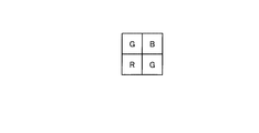
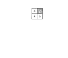
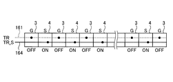
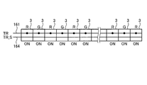
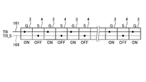
- FIG. 3 is a diagram illustrating a part of a circuit configuration of a pixel array unit applicable to the first embodiment. It is a figure which shows a Bayer arrangement more specifically. It is a figure showing the example which replaced pixel B of a Bayer arrangement with a special pixel.
- 6 is a timing chart schematically showing reading of a pixel signal by an imaging device. It is a figure which shows typically reading of the pixel signal of the special pixel row in which the special pixel was arrange
- FIG. 5 is a diagram schematically illustrating reading of pixel signals of a normal pixel row in which normal pixels are arranged. It is a figure which shows typically reading of the pixel signal of the special pixel row in which the special pixel was arrange
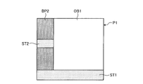
- FIG. 4 is a diagram schematically illustrating an example of a captured image corresponding to image data when a high-luminance subject is captured using an imaging device according to an existing technology.
- FIG. 4 is a diagram schematically illustrating an example of a captured image corresponding to image data when a high-luminance subject is captured using an imaging device according to an existing technology.
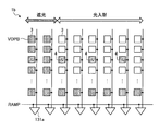
- FIG. 4 is a diagram schematically illustrating a configuration of an imaging device including a pixel array unit in which special pixels are arranged according to an existing technology.
- FIG. 4 is a diagram schematically illustrating an example of a captured image corresponding to image data when a high-luminance subject is captured using an imaging device including a pixel array unit in which special pixels are arranged according to an existing technology.
- 9 is an example timing chart illustrating an operation when a selected row is a normal pixel row according to the existing technology. It is a figure which extracts and shows the normal pixel row by which the some normal pixel in the pixel array part by the existing technique was arrange
- 6 is an example timing chart illustrating an operation when a selected row is a special pixel row according to the existing technology.
- FIG. 2 is a diagram illustrating a configuration of an example of a pixel array unit in the imaging device according to the first embodiment.
- FIG. 17 is an example timing chart illustrating the operation of the imaging device according to the first embodiment.
- FIG. 9 is a diagram illustrating a configuration of an example of a pixel array unit in an imaging device according to a first modification of the first embodiment.
- FIG. 9 is a diagram illustrating a configuration of an example of a pixel array unit in an imaging device according to a second modification of the first embodiment.
- FIG. 13 is a diagram illustrating a configuration of an example of a pixel array unit in an imaging device according to a third modification of the first embodiment.
- FIG. 9 is a block diagram illustrating a configuration of an example of an electronic device according to a second embodiment.
- FIG. 14 is a diagram illustrating a usage example of the imaging device according to the present disclosure.
- FIG. 1 is a block diagram illustrating a solid-state imaging device applicable to the first embodiment of the present disclosure and a schematic configuration example of an electronic device using the solid-state imaging device.
- the imaging apparatus 1 includes a pixel array unit 11, a vertical scanning unit 12, an A / D conversion unit 13, a reference signal generation unit 14, a horizontal scanning unit 15, a pixel signal line 16, a vertical signal It includes a line 17, an output unit 18, and a control unit 19.
- the pixel array unit 11 includes pixels having a photoelectric conversion unit that performs photoelectric conversion on received light, which are arranged in a two-dimensional matrix in the horizontal direction (row direction) and the vertical direction (column direction).
- the photoelectric conversion unit is configured using a photodiode or the like.
- a pixel signal line 16 (first signal line) is connected for each row, and a vertical signal line 17 is connected for each column.
- An end of the pixel signal line 16 that is not connected to the pixel array unit 11 is connected to the vertical scanning unit 12.
- the pixel signal line 16 transmits a control signal such as a drive pulse for reading a pixel signal from a pixel from the vertical scanning unit 12 to the pixel array unit 11.
- An end of the vertical signal line 17 that is not connected to the pixel array unit 11 is connected to an A / D (Analog to Digital) converter 13.
- the vertical signal line 17 transmits a pixel signal read from a pixel to the A / D converter 13.
- the vertical scanning section 12 supplies various signals including a drive pulse to the pixel signal line 16 of the selected pixel row of the pixel array section 11 under the control of the control section 19, thereby converting the pixel signals and the like to the vertical signal lines. 17 is output.
- the vertical scanning unit 12 is configured using, for example, a shift register, an address decoder, and the like.
- the A / D converter 13 includes a column A / D converter 131 provided for each vertical signal line 17 and a signal processor 132.
- the column A / D converter 131 executes a count process for correlated double sampling (CDS) for reducing noise on the pixel signal output from the pixel via the vertical signal line 17. I do.
- the column A / D conversion unit 131 has a comparator 131a and a counter unit 131b.
- the comparator 131a compares the pixel signal input from the pixel via the vertical signal line 17 with the ramp signal RAMP supplied from the reference signal generation unit 14 during the P phase (Preset Phase) period, and compares the comparison result. Output to the counter 131b.
- the P-phase period is a period during which the reset level of the pixel signal is detected in the CDS processing.
- the ramp signal RAMP is, for example, a signal whose level (voltage value) decreases with a constant slope, or a sawtooth signal whose level decreases stepwise. When the level of the ramp signal RAMP is higher than the level of the pixel signal, the comparator 131a outputs a High difference signal to the counter unit 131b.
- the comparator 131a When the level of the ramp signal RAMP is equal to or lower than the level of the pixel signal, the comparator 131a inverts the output and outputs a Low difference signal to the counter unit 131b. Note that the level of the ramp signal RAMP is reset to a predetermined value after the output of the comparator 131a is inverted.
- the counter unit 131b counts down the time from the start of the voltage drop of the ramp signal RAMP to the level equal to or lower than the pixel signal in accordance with the difference signal input from the comparator 131a during the P-phase period. Then, the count result is output to the signal processing unit 132. Further, in the D-phase (Data @ Phase) period, the counter unit 131b has the same or lower level as the pixel signal after the ramp signal RAMP starts the voltage drop according to the difference signal input from the comparator 131a. The time until is counted up, and the count result is output to the signal processing unit 132.
- the D-phase period is a detection period for detecting the signal level of the pixel signal in the CDS processing.
- the signal processing unit 132 performs CDS processing and A / D conversion processing based on the count result of the P-phase period and the count result of the D-phase period input from the counter unit 131b to generate digital image data, Output to the output unit 18.
- the reference signal generator 14 generates a ramp signal RAMP based on the control signal input from the controller 19, and outputs the generated ramp signal RAMP to the comparator 131a of the A / D converter 13.
- the reference signal generator 14 is configured using, for example, a D / A conversion circuit.
- the horizontal scanning unit 15 performs selective scanning for selecting each column A / D conversion unit 131 in a predetermined order, so that each column A / D conversion unit 131 temporarily holds the data.
- the counting result is sequentially output to the signal processing unit 132.
- the horizontal scanning unit 15 is configured using, for example, a shift register, an address decoder, and the like.
- the output unit 18 performs predetermined signal processing on the image data input from the signal processing unit 132 and outputs the processed image data to the outside of the imaging device 1.
- the control unit 19 controls driving of the vertical scanning unit 12, the A / D conversion unit 13, the reference signal generation unit 14, the horizontal scanning unit 15, and the like.
- the control unit 19 is configured using, for example, a timing generator or the like.
- the control unit 19 generates various drive signals serving as references for the operations of the vertical scanning unit 12, the A / D conversion unit 13, the reference signal generation unit 14, and the horizontal scanning unit 15.
- the imaging device 1 configured as described above is a column AD type CMOS (Complementary Metal Oxide Semiconductor) image sensor in which the column A / D converter 131 is arranged for each column.
- the number of the A / D converters 13 is one. However, for example, two A / D converters 13 are provided in the vertical direction of the pixel array unit 11, and the odd and even columns of the pixel array unit 11 are provided. May be divided in the vertical direction to output a pixel signal.
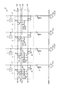
- FIG. 2 is a diagram illustrating a part of the circuit configuration of the pixel array unit 11 applicable to the first embodiment.
- the pixel array unit 11 includes a constant current source 2, a pixel 3 (hereinafter, referred to as “normal pixel 3”), and a pixel 4 (hereinafter, referred to as “special pixel 4”).
- a pixel 3 is connected to a first transfer signal line 161, a reset signal line 162, and a row selection signal line 163 as a pixel signal line 16.
- a reset signal line 162, a row selection signal line 163, and a second transfer signal line 164 are connected to each special pixel 4 as a pixel signal line 16.
- the constant current source 2 is provided for each vertical signal line 17.
- the constant current source 2 is configured using an N-channel MOS (metal-oxide-semiconductor field-effect) transistor (hereinafter abbreviated as “NMOS”).
- NMOS metal-oxide-semiconductor field-effect transistor
- the constant current source 2 has one end grounded and the other end connected to the vertical signal line 17.
- the normal pixels 3 are arranged in a two-dimensional matrix on the pixel array unit 11.
- the normal pixel 3 includes a photoelectric conversion unit 31, a transfer switch 32, a floating diffusion 33 (hereinafter abbreviated as "FD33"), a reset switch 34, an amplification transistor 35, and a row selection switch 36.
- the photoelectric conversion unit 31 performs photoelectric conversion on the received light to generate signal charges for an image.
- the photoelectric conversion unit 31 is configured using, for example, a PN junction photodiode.
- the photoelectric conversion unit 31 has an anode terminal grounded and a cathode terminal connected to the FD 33 via the transfer switch 32.
- the photoelectric conversion unit 31 functions as a first photoelectric conversion unit.
- the transfer switch 32 has one end connected to the photoelectric conversion unit 31 and the other end connected to the FD 33. Further, the transfer switch 32 is connected to the first transfer signal line 161. When the transfer pulse TR is supplied via the first transfer signal line 161, the transfer switch 32 is turned on (closed), and transfers the signal charge photoelectrically converted by the photoelectric conversion unit 31 to the FD 33.
- the FD 33 temporarily holds the signal charge transferred from the photoelectric conversion unit 31 and converts the signal charge into a voltage corresponding to the charge amount.
- the reset switch 34 has one end connected to the FD 33 and the other end connected to the power supply voltage. Further, the reset switch 34 is connected to the reset signal line 162. The reset switch 34 is turned on when a reset pulse RST is supplied via the reset signal line 162, and resets the potential of the FD 33 to a predetermined potential by discharging the charge of the FD 33 to the power supply voltage.
- the amplification transistor 35 has one end connected to the power supply voltage and the other end connected to the row selection switch 36. Further, an FD 33 is connected to a gate end of the amplification transistor 35.
- the amplification transistor 35 functions as a source follower together with the constant current source 2 connected via the vertical signal line 17.
- the amplification transistor 35 outputs a reset signal (reset level) indicating a level according to the potential of the FD 33 after being reset by the reset switch 34 to the vertical signal line 17. Further, the amplification transistor 35 outputs an image pixel signal indicating a level corresponding to the charge amount of the signal charge held in the FD 33 after the transfer of the signal charge from the photoelectric conversion unit 31 by the transfer switch 32 to the vertical signal line 17.
- the row selection switch 36 has one end connected to the amplification transistor 35 and the other end connected to the vertical signal line 17. Further, the row selection switch 36 is connected to the row selection signal line 163. When the row selection signal SEL is supplied from the row selection signal line 163, the row selection switch 36 is turned on, and the reset signal or the pixel signal (first signal) output from the amplification transistor 35 is sent to the vertical signal line 17 Output.
- One end of the vertical signal line 17 is connected to the comparator 131a or 131a_S of the A / D converter 13.
- the comparator 131a connected to the vertical signal line 17 to which the special pixel 4 is connected is shown as a comparator 131a_S.
- the transfer switch 32, the reset switch 34, the amplification transistor 35, and the row selection switch 36 of the normal pixel 3 configured as described above are configured using, for example, an NMOS or P-channel MOS transistor (abbreviated as PMOS).
- the normal pixel 3 includes any one of an R (red) filter, a G (green) filter, and a B (blue) filter stacked on the light receiving surface of the photoelectric conversion unit 31.
- the normal pixels 3 form a Bayer array on the pixel array unit 11.
- FIG. 3A is a diagram showing the Bayer arrangement more specifically. As illustrated in FIG. 3A, the Bayer arrangement is configured by a set including one pixel R and one pixel B and two pixels G, respectively.
- the special pixels 4 are arranged at predetermined intervals in a predetermined pixel row.
- the special pixels 4 are alternately arranged with the pixels G in a predetermined pixel row.
- the special pixels 4 are sequentially located at positions corresponding to the pixels B in the Bayer array of the normal pixels 3 in a predetermined pixel row and adjacent to the pixels G in the same row. Be placed.
- FIG. 3B is a diagram illustrating an example in which the pixel B in the Bayer array illustrated in FIG. 3A is replaced with a special pixel 4 (pixel S).
- the array including the pixel S illustrated in FIG. 3B is configured by a set including one pixel R, one pixel G, one pixel B, and one pixel S.
- the special pixel 4 has the same configuration as the normal pixel 3, and includes a photoelectric conversion unit 41, a transfer switch 42, a floating diffusion 43 (hereinafter simply referred to as “FD43”), a reset switch 44, and an amplification transistor 45. , A row selection switch 46.
- the special pixel 4 includes a special filter stacked on the light receiving surface of the photoelectric conversion unit 41.
- the transfer switch 42 is connected to the second transfer signal line 164, and the transfer pulse TR_S is supplied from the second transfer signal line 164.
- the configuration of the special pixel 4 other than these is the same as that of the normal pixel 3.
- the photoelectric conversion unit 41 functions as a second photoelectric conversion unit.
- the special pixel 4 is a pixel other than the pixels (for example, the pixel R, the pixel G, and the pixel B) for acquiring color information and luminance information in a visible light region to form a full-color image.
- Examples of the special pixel 4 include an infrared light pixel, a white pixel, a monochrome pixel, a black pixel, a polarization pixel, and an image plane phase difference pixel.
- an infrared filter capable of receiving infrared light is laminated on a light receiving surface of the photoelectric conversion unit 41.
- a white filter capable of receiving all visible light of red, green and blue is laminated on the light receiving surface of the photoelectric conversion unit 41.
- a transparent filter is laminated on the light receiving surface of the photoelectric conversion unit 41.
- a light-blocking filter is laminated on the light receiving surface of the photoelectric conversion unit 41.
- a polarization pixel is a pixel using a polarization element for receiving polarized light.
- the image plane phase difference pixel an aperture filter having only a predetermined area opened on the light receiving surface of the photoelectric conversion unit 41 is laminated. More specifically, the image plane phase difference pixel is composed of a pixel on which an aperture filter having an opening in, for example, a left half area of the light receiving surface of the photoelectric conversion unit 41 is laminated, and a light receiving surface of another photoelectric conversion unit 41. A pair of pixels, in which an aperture filter having an opening in the right half region, is stacked, and a pair of pixels, and a distance measurement is performed based on a phase difference of light received by the two pixels.
- the pixel signal obtained by photoelectrically converting the light received by the special pixel 4 can realize a different function from the pixel signal obtained by photoelectrically converting the light received by the normal pixel 3.
- the special pixel 4 or the photoelectric conversion unit 41 of the special pixel 4 is expressed as “S”.
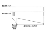
- FIG. 4 is a timing chart schematically showing reading of a pixel signal by the imaging device 1.
- the horizontal axis indicates time.
- the output timing of the vertical synchronization pulse is shown in the upper part, and the output timing of the horizontal synchronization pulse in the vertical scanning unit 12 is shown in the middle part.
- FIG. 4 shows a case where the imaging device 1 reads out pixel signals of one frame.
- the control unit 19 first performs a special operation from a special pixel row in which the special pixels 4 of the pixel array unit 11 are arranged according to, for example, a vertical synchronization pulse and a horizontal synchronization pulse input from outside the imaging apparatus 1.
- the pixel signals (second signals) of the pixels 4 are sequentially read.
- the control unit 19 causes the vertical scanning unit 12 to supply the transfer pulse TR_S in a High state to the special pixel 4 via the second transfer signal line 164 in the special pixel row.
- the normal pixel 3 With the normal pixel 3 turned off, a pixel signal is read from the special pixel 4. In this case, the normal pixel 3 is in an accumulation state (exposure state) in which light is received and signal charges are accumulated.
- the control unit 19 After reading out the pixel signals (second signals) from the special pixels 4 of all the special pixel rows, the control unit 19 outputs the pixel signals (first signals) from each normal pixel 3 for each row of the pixel array unit 11. Read sequentially. Specifically, the control unit 19 sequentially reads out the pixel signals of the normal pixels 3 from the normal pixel row and the special pixel row. When reading the pixel signal from the normal pixel row in which only the normal pixels 3 are arranged, for example, the control unit 19 causes the vertical scanning unit 12 to transfer the signal in the High state via the first transfer signal line 161 as illustrated in FIG. The pulse TR is supplied to the normal pixel 3.
- the control unit 19 When reading out the pixel signals from the normal pixels 3 in the special pixel row in which the special pixels 4 are arranged, the control unit 19 causes the vertical scanning unit 12 to transmit the pixel signals via the first transfer signal line 161 as shown in FIG. Only the transfer pulse TR in the High state is supplied to the normal pixel 3. That is, the control unit 19 sequentially reads out the pixel signals only from the normal pixels 3 in a state where the transfer switch 42 of the special pixel 4 in the special pixel row is turned off. At this time, the output of the special pixel 4 is equivalent to the black level (corresponding to the power supply voltage) because the transfer switch 42 is in the OFF state.
- the pixel signal of the special pixel 4 is interpolated by performing a demosaicing process using a pixel signal of a peripheral pixel using, for example, an image processing device provided outside the imaging device 1.
- the imaging apparatus 1 first performs the reading method of reading the pixel signals of the special pixels 4 from all the special pixel rows, and then sequentially reading the pixel signals from the normal pixels 3 for each row of the pixel array unit 11. .
- this reading method is referred to as divided reading.
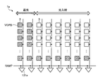
- FIG. 8 is a diagram schematically illustrating a schematic configuration of an imaging device 1a according to the existing technology including the pixel array unit 11 in which only the normal pixels 3 are arranged as the pixels and the special pixels 4 are not arranged.
- FIG. 9 is a diagram schematically illustrating an example of a captured image corresponding to image data when a high-luminance subject is captured using the imaging device 1a in FIG. In FIG.
- each of the normal pixels 3 in the left two columns in the vertical direction is shielded from light to form a light-shielded pixel VOPB, and each lowermost normal pixel in the horizontal direction is shielded from light to form a light-shielded pixel VOPB.
- the imaging device 1a illustrated in FIG. 8 captures a high-luminance subject in a part of the angle of view
- the imaging device 1a is affected by power supply noise due to simultaneous inversion of the A / D conversion unit 13.
- streaking ST1 occurs near the subject area OB1 in the image P1.
- no streaking has occurred in the dark area BP2 (background area).
- FIG. 10 shows a configuration of an imaging device 1b including a pixel array unit 11 in which special pixels 4 are arranged in predetermined rows at predetermined intervals with respect to ordinary pixels 3 arranged in a two-dimensional matrix according to existing technology. It is a figure which shows schematically. In this case, the special pixel 4 is arranged so as to replace the normal pixel 3 at a predetermined position.
- FIG. 11 is a diagram corresponding to FIG. 9 described above, and is a diagram schematically illustrating an example of a captured image corresponding to image data when a high-luminance subject is captured using the imaging device 1b in FIG. is there.
- the image P1 when a high-luminance subject is imaged in a part of the angle of view, the image P1 is affected by power supply noise due to simultaneous inversion of the A / D conversion unit 13, and the image P1 has a subject area OB1. Streaking ST1 occurs in the vicinity, and streaking ST2 occurs in a special pixel row in the dark area BP2.
- streaking may occur in a special pixel row even in the subject area OB1.
- FIG. 12 is an example timing chart showing an operation according to the existing technology when a selected row is a normal pixel row.
- FIG. 13 is a diagram showing an excerpt of a normal pixel row in which a plurality of normal pixels 3 in the pixel array unit 11 are arranged according to the existing technology.
- the control unit 19 a High state row selection signal SEL of the selected row at time t 100, the row selection switch 36 of the selected row to the ON state. High state of the row selection signal SEL is maintained until time t 105 to read the pixel signals of the selected row is completed.
- the control unit 19 at time t 101, the reset pulse RST of the selected row a High state.
- the amplification transistor 35 in the selected row outputs a reset signal based on the charge amount of the FD 33 after being reset by the reset switch 34 to the vertical signal line 17.
- the reset pulse RST is at t 102 and Low state.
- each of the transfer pulse TR and the transfer pulse TR_S the selected row to a High state, the respective transfer pulse and a Low state at time t 104.
- the transfer switch 32 of the selected row Period from the time point t 103 to time t 104, as shown in FIG. 8, the transfer switch 32 of the selected row are turned on.
- the amplifying transistor 35 outputs the pixel signal VSL to the vertical signal line 17 according to the amount of the signal charge received and photoelectrically converted by the photoelectric conversion unit 31. In this case, the level of the pixel signal VSL decreases from a predetermined potential (black level) according to the amount of signal charge.
- FIG. 14 is a timing chart illustrating an example of an operation performed when a selected row is a special pixel row according to the existing technology.
- FIG. 15 is a diagram illustrating a special pixel row in which a plurality of normal pixels 3 and special pixels 4 are arranged in the pixel array unit 11 according to the existing technology.
- the control unit 19 As shown in FIG. 14, the control unit 19, a High state row selection signal SEL of the selected row at time t 110, a row selection switch 36 of the normal pixel of the selected row, each row select switch of each special pixel 4 And 46 are turned on. High state of the row selection signal SEL is maintained until time t 115 to read the pixel signals of the selected row is completed.
- the control unit 19, at time t 111, the reset pulse RST of the selected row a High state.
- the amplification transistor 35 in the selected row outputs a reset signal based on the charge amount of the FD 33 after being reset by the reset switch 34 to the vertical signal line 17.
- the amplification transistor 45 in the selected row outputs a reset signal based on the charge amount of the FD 43 after being reset by the reset switch 44 to the vertical signal line 17.
- the reset pulse RST is a Low state when t 112.
- the control unit 19 At a later time t 113, the control unit 19, a transfer pulse TR of the selected row to a High state and a Low state transfer pulse TR at time t 114.
- the transfer switch 32 of the selected row are turned on.
- the amplifying transistor 35 outputs the pixel signal VSL to the vertical signal line 17 according to the amount of the signal charge received and photoelectrically converted by the photoelectric conversion unit 31.
- the level of the pixel signal VSL decreases from a predetermined potential (black level) according to the amount of signal charge.
- the pixel signal VSL from the normal pixel 3 at this time is shown as a pixel signal VSL_N in FIG.
- the transfer pulse TR_S since the transfer pulse TR_S remains in the Low state, the off state is maintained in each of the transfer switches 42 in the selected row as shown in FIG. As a result, the charge is not transferred from the photoelectric conversion unit 41 to the FD 43, and the charge stored in the FD 43 remains at the reset level. Therefore, a signal of the reset signal level is output from the amplification transistor 45 in the selected row to the vertical signal line 17 as the pixel signal VSL_S. As illustrated in FIG. 15, the level of the pixel signal VSL_N maintains a constant value (black level) without lowering due to the influence of power supply noise. Therefore, when the special pixels 4 are arranged at predetermined intervals in predetermined rows of the pixel array unit 11, streaking occurs due to the effect of the level of the pixel signal VSL_S of the special pixels 4.
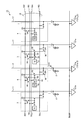
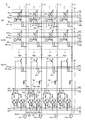
- FIG. 16 is a diagram illustrating an example of a configuration of the pixel array unit 11a in the imaging device 1 according to the first embodiment.
- the pixel array unit 11a is applied as the pixel array unit 11 in the imaging device 1 shown in FIG.
- a dummy row is added to the pixel array unit 11 a in the pixel array unit 11 a described in FIG. 2.
- the pixel array unit 11a includes a row in which a plurality of normal pixels 3 and special pixels 4 are arranged (for example, N rows in FIG. 16) and a row in which a plurality of normal pixels 3 are arranged and no special pixels 4 are arranged ( For example, (N + 2 rows in FIG. 16), row selection signal lines 163a and 163b are arranged instead of the row selection signal line 163 in FIG.
- the row selection signal line 163a is connected to each normal pixel 3 in a column not including the special pixel 4.
- the row selection signal line 163b is connected to each normal pixel 3 and each special pixel 4 in a column including the special pixel 4.
- N rows where the special pixels 4 are arranged and N ⁇ 2 rows where the pixels B are arranged as the normal pixels 3 are described, and N rows where the pixels G and the pixels R are arranged as the normal pixels 3 are shown.
- the description of line -1 is omitted.
- the row selection signal line 163a is connected to each normal pixel 3 in the column that does not include the special pixel 4 and the row selection signal line 164b is connected to the normal pixel 3 in the column that includes the special pixel 4.
- the special pixel 4 is arranged at a position corresponding to the pixel B in the Bayer array.
- the dummy row includes a dummy section 500a corresponding to each vertical signal line 17.
- Each dummy unit 500a includes a transistor 50 whose buffer unit is configured by a source follower amplifier, a dummy selection switch 51a or 51b, and a holding unit 501.
- dummy row signal lines 180 dummy row selection signal lines 181 and 182, read control lines 183 and 184 (third signal lines), and holding control lines 185 and 186 (second ) Are connected.
- the transistor 50 is, for example, a MOS transistor, in which the power supply voltage is connected to the drain, the gate is connected to the holding unit 501, and the source is connected to one end of the dummy selection switch 51a or 51b. .
- the other ends of the dummy selection switches 51a and 51b are connected to the vertical signal line 17.
- the transistor 50 is used as a source follower amplifier using a MOS transistor.
- the dummy selection switch 51a is connected to the dummy row selection signal line 181.
- the dummy selection switch 51a is turned on when the dummy row selection signal SEL DMY supplied via the dummy row selection signal line 181 is High.
- the dummy selection switch 51b is connected to the dummy row selection signal line 182.
- Dummy selection switch 51b, the dummy row selection signal SEL_S DMY supplied via a dummy row selection signal line 182 is turned on at the High (high) state.
- Each holding unit 501 includes a P-phase holding unit including an analog switch 52a, a capacitor 53a, and a holding selection switch 54a, and a D-phase holding unit including an analog switch 52b, a capacitor 53b, and a holding selection switch 54b.
- the holding control line 185 of the analog switch 52a is connected to the terminal 55a1.
- Analog switch 52a is held control pulse SH_P supplied to the holding control line 185 is in the High state, connects the terminal 55a 2 and the terminal 55a 3 in both directions.
- Terminal 55a 2 of the analog switch 52a is connected to one end of the storage selection switch 54a, and one end of the capacitor 53a, the. The other end of the capacitor 53a is set to the ground potential.
- the other end of the hold selection switch 54a is connected to the gate of the transistor 50.
- the read control line 183 is connected to the holding selection switch 54a.
- the holding selection switch 54a is turned on when the read control signal RD_P supplied from the read control line 183 is High.
- the terminal 55a 3 of the analog switches 52a are connected to the vertical signal line 17.
- the D-phase holding unit has the same configuration as the above-described P-phase holding unit. That is, in the D-phase holding unit, the analog switch 52b is held control line 186 is connected to the terminal 55b 1, holding control pulse SH_D supplied to the holding control line 186 is in the High state, the terminal 55b 2 and the terminal 55b 3 Is connected in both directions. Terminals 55b 2 of the analog switch 52b is, one end of the holding selection switch 54b, the other end connected to the one end of the capacitor 53b to the ground potential. The other end of the holding selection switch 54b is connected to the gate of the transistor 50 in common with the holding selection switch 54a described above.
- the read control line 184 is connected to the holding selection switch 54b, and the read control signal RD_D supplied from the read control line 184 is turned on in a high state.
- the terminal 55b 3 of the analog switch 52b is connected to the vertical signal line 17 in common with the terminal 55a 3 of the analog switch 52a.
- the output of the special pixel 4 is connected to the same vertical signal line 17 as the special pixel 4 in the row where the special pixel 4 is not arranged by controlling the operation of the above-described pixel array unit 11a.
- the output can be replaced by the output of the normal pixel 3 at the position corresponding to the special pixel 4 in the Bayer arrangement.
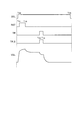
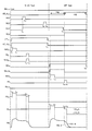
- FIG. 17 is an example timing chart showing the operation of the imaging device according to the first embodiment.
- FIG. 17 shows the output of the D phase of the special pixel 4 in the same column as that of the special pixel 4 and the normal pixel 3 (pixel B) arranged at the position corresponding to the special pixel 4 in the Bayer arrangement. Is replaced with the D-phase output of FIG. Note that reading of each row is performed by selecting each row as a selected row in the order of N ⁇ 2 row, N ⁇ 1 row, and N row.
- FIG. 17 shows the reading operation of N ⁇ 2 row and N row. The description regarding the read operation of the (N-1) th row is omitted.
- the control unit 19 maintains the low state of the dummy row selection signal SEL DMY during the reading period of the (N ⁇ 2) th row. Therefore, the dummy selection switch 51 a in the dummy section 500 a in the column where the special pixel 4 is not arranged maintains the off state (open state), and the voltage held in the capacitors 53 a and 53 b is not supplied to the vertical signal line 17.
- Control unit 19 in response to the start of the N-2-line readout period, a row select signal SEL N-2 and SEL_S N-2 at time t 00, respectively a High state, respectively turning on the row select switches 36 and 46a And Next, the control unit 19, the period of time t 02 from the time t 01, the reset pulse RST to High state. As a result, the amplification transistors 35 in the (N ⁇ 2) th row, which is the selected row, output a reset signal based on the accumulated charges in the FD 33 after being reset by the reset switch 34 to the vertical signal line 17.
- Control unit 19 at time t 03 after from the Low state to the reset pulse RST at 02 predetermined time (e.g. timing pixel signal VSL is considered to have stabilized), as well as a read control signal RD_P a High state ,
- the holding control pulse SH_P is kept High until time t 04 .
- Control unit 19 after a predetermined time period from time t 06 from the time point t 05 of time t 04, each of the transfer pulse TR and the transfer pulse TR_S of N-2-line to a High state.
- each transfer switch 32 included in the normal pixels 3 in the (N ⁇ 2) th row is turned on.
- the amplifying transistor 35 outputs the pixel signal VSL to the vertical signal line 17 according to the amount of the signal charge received and photoelectrically converted by the photoelectric conversion unit 31. In this case, the level of the pixel signal VSL decreases from a predetermined potential (black level) according to the amount of signal charge.
- the hold control pulse SH_D a High state .
- the holding selection switch 54b together with is turned on, the terminal 55b 2 and the terminal 55b 3 in the analog switch 52b is connected. Since the dummy selection switch 51b maintains the off state, the voltage of the pixel signal VSL is held in the capacitor 53b.
- Control unit 19 the time t 09 in the row selection signal SEL N-2 and SEL_S N-2 as a Low state, respectively, to terminate the read period of the N-2 line.
- the # N-1 row includes only normal pixels 3 and no special pixels 4 as pixels. Further, the arrangement of the pixels in the (N-1) th row is different from the (N-2) th row in which the pixels G and B in the Bayer arrangement are arranged, and the pixels R and the pixels G are arranged. That is, the arrangement of the pixels in the (N-1) th row does not correspond to the arrangement of the Nth row in which the pixel B of the pixels G and B in the Bayer array is replaced with the pixel S which is the special pixel 4.
- the read operation of the # N-1 row is substantially the same as the above-described read operation of the N-2 row except for the holding control pulses SH_P and SH_D. That is, in the read operation of the (N-1) th row, the hold control pulses SH_P and SH_D are maintained in the Low state. Therefore, in the read operation of the (N-1) th row, the holding of the voltage of the reset signal in the capacitor 53a and the holding of the voltage of the pixel signal VSL in the capacitor 53b are not performed. That is, as the voltages held in the capacitors 53a and 53b, the voltage of the reset signal and the voltage of the pixel signal VSL, which are held in the read operation of the (N-2) th row, are maintained.
- N rows which are rows including the special pixels 4, will be described.
- the control unit 19 maintains the low state of the dummy row selection signal SEL DMY during the reading period of the (N ⁇ 2) th row. Therefore, the dummy selection switch 51a in the dummy section 500a in the column where the special pixel 4 is not arranged maintains the off state, and the voltage held in the capacitors 53a and 53b is not supplied to the vertical signal line 17.
- the dummy select switch 51b in the dummy portion 500a of the column special pixels 4 are arranged is turned off until the time point t 24, during the period from the start of the N rows of the readout period to time t 24, the capacitors 53a and The voltage held in 53b is not supplied to the vertical signal line 17.
- control unit 19 maintains the holding control pulses SH_P and SH_D in the low state during the reading period of N rows.
- Control unit 19 in response to the start of the reading period, respectively a High state the row selection signals SEL N and SEL_S N at time t 20, and respectively turning on the row select switches 36 and 46a.
- the control unit 19 the period of time t 22 from the time t 21, the reset pulse RST to High state.
- the amplification transistor 35 included in the normal pixel 3 in the selected row N outputs the reset signal based on the accumulated charge of the FD 33 after being reset by the reset switch 34 to the vertical signal line 17.
- the amplification transistor 45 included in the special pixel on the Nth row outputs a reset signal based on the accumulated charges of the FD 43 after being reset by the reset switch 44 to the vertical signal line 17.
- Time t 21 to the reset pulse RST is set to High state, the start timing of the P phase.
- the read control signal RD_P is in the High state at the timing corresponding to the time point t 03 in the read period of the immediately preceding row, ie, the (N ⁇ 1) -th row, similarly to the above-mentioned N ⁇ 2 row.
- dummy row select signal SEL_S DMY until time t 24, there is a Low state. Therefore, the dummy selection switch 51b in the dummy section 500a in the column where the special pixels 4 are arranged also maintains the OFF state, and the voltage held in the capacitors 53a and 53b is not supplied to the vertical signal line 17 during this period.
- Time t 23 is, for example, the timing at which the pixel signal VSL is considered to have stabilized.
- Control unit 19 the period of time t 25 from the time t 24 after a predetermined time point t 23, the N rows, usually a High state transfer pulse TR supplied to the pixel 3.
- each transfer switch 32 included in each normal pixel 3 are turned on.
- the amplifying transistor 35 outputs the pixel signal VSL to the vertical signal line 17 according to the amount of the signal charge received and photoelectrically converted by the photoelectric conversion unit 31.
- the level of the pixel signal VSL decreases from a predetermined potential (black level) according to the amount of signal charge. That is, the time point t 24 is the transition timing from the P phase to the D phase.
- control unit 19 the period of time t 25 from the time t 24, the N rows, a transfer pulse TR_S supplied to a special pixel 4, is maintained in Low state. Accordingly, the off state of each transfer switch 42 included in each special pixel 4 in the N-th row is maintained, and the pixel signal VSL corresponding to the amount of signal charge received and photoelectrically converted by the photoelectric conversion unit 41 is a vertical signal. Not output on line 17.
- Control unit 19 further, the dummy row selection signal SEL_S DMY a High state at time t 24.
- the holding control pulse SH_D is low state maintained in the readout period of the N rows, the analog switch 52 b, and the terminal 55b 2 and the terminal 55b 3 not connected. As a result, the pixel signal VSL from the special pixel 4 is not output to the vertical signal line 17 and the voltage held in the capacitor 53b is output to the vertical signal line 17 via the transistor 50.
- the vertical signal line 17 corresponds to the position of the special pixel 4 in the readout operation of the (N ⁇ 2) th row in the Bayer array instead of the pixel signal VSL output from the special pixel 4.
- the voltage of the pixel signal VSL output from the normal pixel 3 which is the pixel B adjacent to the special pixel 4 in the Bayer arrangement unit is supplied.
- the voltage of the FD33 as exemplified as the voltage FD N _N 17, similar to the N-2 rows of FD33 voltage (FD N-2), varies according to the usual sequence.
- the pixel signal VSL_N also changes according to a normal sequence, similarly to the N-2th row.
- the row selection switch 46a for row selection signal SEL_S N is a Low state at time t 24 the reading of the N rows is turned off, the voltage of the FD43 is not output to the vertical signal line 17 . Therefore, the voltage of the reset signal is maintained as illustrated as the voltage FD N _S in FIG. Since the pixel signal VSL_S is not output from the FD 43, the voltage decreases faster than the pixel signal VSL_N.
- Control unit 19 the holding selector switch 54b of the read control signal RD_D as Low state is turned off at time t 26, to terminate the reading from the capacitor 53b. At time t 26 , the control unit 19 sets the row selection signal SEL N to the Low state, and ends the reading period of the (N ⁇ 2) th row.
- the position of the special pixel 4 corresponds to the position in the Bayer array, and is adjacent in the Bayer array unit.
- the holding unit 501 holds the pixel signal VSL read from the normal pixel 3 (pixel B) in the (N-2) th row. Then, the imaging apparatus 1 does not read out the pixel signal VSL from the special pixel 4 during the readout operation on the N rows including the special pixel 4 and reads out the normal pixel 3 held in the holding unit 501.
- the supplied pixel signal VSL is supplied to the vertical signal line 17.
- the imaging apparatus 1 according to the first embodiment can reduce streaking caused by the special pixels 4 by this operation. More specifically, the imaging device 1 according to the first embodiment converts the pixel signal VSL of the special pixel 4 in the Nth row from the output of the special pixel 4 in the N-2th row to the special pixel 4
- the positions of the Bayer arrangements correspond to each other, and can be replaced with pixel signals VSL by adjacent normal pixels 3 (pixels B) in Bayer arrangement units. Therefore, the output level of the pixel signal VSL can be made uniform between the row including only the normal pixel 3 as the pixel and the row including the normal pixel 3 and the special pixel 4 as the pixel, and the streaking caused by the special pixel 4 is reduced. It is possible.
- Patent Document 1 streaking is suppressed by securing a horizontal light-shielding portion in an image sensor and obtaining a streaking correction amount for each row based on a black-level output signal of the vertical light-shielding portion.
- it is necessary to secure a large area of the horizontal light shielding portion in order to reduce the influence of the horizontal stripe due to random noise. Therefore, the area per unit chip in which the pixel array portion is formed increases, the height per wafer decreases, and the cost increases.
- streaking is achieved by adding a dummy row not including a pixel configuration and controlling each switch without implementing a streaking correction function having a large-scale pixel area (horizontal light-shielding portion). Has been reduced. Therefore, the area per unit chip in which the pixel array portion is formed can be suppressed, and an increase in cost can be suppressed.
- the imaging device 1 can replace the P-phase output of the special pixel 4 with the P-phase output of the normal pixel 3.
- the control unit 19 the read operation of the N rows, the read control signal RD_P, a Low state at time t 20, or earlier, to a High state at time t 24. Further, the control unit 19 maintains the low state of the read control signal RD_D during the read period of N rows. Further, the control unit 19, a row selection signal SEL_S N, and a Low state at the time point t 20, the High state at time t 24.
- the voltage of the reset signal held in the capacitor 53a during the read operation of the (N ⁇ 2) th row is supplied to the vertical signal line 17 during the P phase of the read operation of the Nth row.
- the P-phase output of the special pixel 4 is replaced with the P-phase output of the normal pixel 3.
- each of the P-phase and the D-phase of the special pixel 4 can be replaced with the output of the P-phase and the D-phase of the normal pixel 3.
- the control unit 19 the read operation of the N rows, the read control signal RD_P, a time point t 20 Oite High state, while a Low state at the time point t 23, the read control signal RD_D, time t a High state at 24, the Low state when t 26.
- the control unit 19, a dummy row select signal SEL_S DMY, during the reading period of the N rows is maintained at the High state.
- the voltage of the reset signal held in the capacitor 53a during the read operation of the (N ⁇ 2) th row is supplied to the vertical signal line 17 during the P phase of the read operation of the Nth row.
- the P-phase output of the special pixel 4 is replaced with the P-phase output of the normal pixel 3.
- the voltage of the pixel signal VSL held in the capacitor 53b during the readout operation of the N-2th row is supplied to the vertical signal line 17, and the D phase of the special pixel 4 is Is replaced by the D-phase output of the normal pixel 3.
- the reset signal voltage is not held in the capacitor 53a and the pixel signal VSL voltage is not held in the capacitor 53b in the read operation of the (N-1) th row has been described. It is not limited to. That is, in the read operation of the (N-1) -th row including only the normal pixel 3, the reset signal and the voltage of the pixel signal VSL can be held in the capacitors 53a and 53b. In this case, the read operation of the (N-1) -th row is the same as the above-described read operation of the (N-2) -th row, and a description thereof will be omitted.
- each voltage is held in each of the capacitors 53a and 53b in the (N-1) th row, and each voltage held in each of the capacitors 53a and 53b in the Nth row. Is effective.
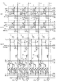
- FIG. 18 is a diagram illustrating a configuration of an example of the pixel array unit 11b in the imaging device 1 according to the first modification of the first embodiment.
- the pixel array unit 11b shown in FIG. 18 uses a voltage follower amplifier instead of the transistor 50 in the pixel array unit 11a of FIG. 16 in replacing the buffer unit for supplying the voltage held in the capacitor 53a or 53b to the vertical signal line 17. 70 (dummy section 500b). In FIG. 18, the path of the power supplied to the voltage follower amplifier 70 is omitted.
- the voltage held in the capacitor 53a or 53b is supplied to the vertical signal line 17 via the transistor 50. Therefore, the voltage supplied to the vertical signal line 17 is attenuated with respect to the voltage held in the capacitor 53a or 53b.
- the voltage held in the capacitor 53a or 53b is supplied to the vertical signal line 17 via the voltage follower amplifier 70. I have to. Therefore, the voltage held in the capacitor 53a or 53b can be supplied to the vertical signal line 17 while minimizing attenuation.
- the output level of the pixel signal VSL is more improved between the row including only the normal pixels 3 as the pixels and the row including the normal pixels 3 and the special pixels 4 as the pixels. High-precision alignment can be achieved, and streaking caused by the special pixels 4 can be effectively reduced.
- FIG. 19 is a diagram illustrating a configuration of an example of the pixel array unit 11c in the imaging device 1 according to the second modification of the first embodiment.
- one end of the switch 60 is connected to the dummy voltage line 187, and the other end is connected to the gate of the transistor 50.
- One end of the switch 61 is connected to a connection point between the other end of the switch 60 and the gate of the transistor 50, and the other end is connected to the other end of the holding selection switch 54a and the other end of the holding selection switch 54b in the holding unit 501. Is connected to the connection point.
- control unit 19 exclusively controls the on / off state of the switch 60 and the on / off state of the switch 61.
- the switch 60 is turned off and the switch 61 is turned off, the same operation as the read operation described with reference to FIG. 17 can be performed.
- the switch 60 when the switch 60 is on and the switch 61 is off, the dummy voltage V DMY supplied from the dummy voltage line 187 is supplied to the gate of the transistor 50.
- the dummy selection switch 51b is turned on in this state, and the row selection switch 46a of the special pixel 4 is turned off, so that the dummy voltage V DMY is supplied via the transistor 50 to the vertical signal line 17.
- the pixel signal VSL of the special pixel 4 can be replaced by the dummy voltage VDMY .
- the streaking is reduced as compared with the case where the voltage held in the capacitor 53a or 53b is replaced with the pixel signal VSL of the special pixel 4 in the read operation of the (N-2) th row. Accuracy is reduced.
- the control by the read control signals RD_P and RD_D and the holding control pulses SH_P and SH_D becomes unnecessary, the load on the control unit 19 can be reduced, for example.
- Which of the switches 60 and 61 is turned on can be appropriately selected according to, for example, the load of the control unit 19, the power consumption of the device, the purpose of use of the imaging device 1, and the like.
- FIG. 20 is a diagram illustrating a configuration of an example of the pixel array unit 11d in the imaging device 1 according to the third modification of the first embodiment.
- the pixel array unit 11d illustrated in FIG. 20 is an example in which the transistor 50 of the pixel array unit 11c illustrated in FIG. 19 is replaced with a voltage follower amplifier 70 (dummy unit 500d).
- one end of the switch 60 is connected to the dummy voltage line 187 for supplying the dummy voltage VDMY , and the other end is connected to the input terminal of the voltage follower amplifier 70.
- One end of the switch 61 is connected to a connection point between the other end of the switch 60 and the input end of the voltage follower amplifier 70, and the other end is connected to the other end of the holding selection switch 54a and the holding selection switch 54b in the holding unit 501. Connected to the connection point with the other end.
- the operation and effect of the pixel array unit 11d according to the third modification of the first embodiment are the same as the operation and effect of the pixel array unit 11c according to the second modification of the first embodiment described above. Therefore, the description here is omitted.
- the effect obtained by replacing the transistor 50 of the pixel array unit 11c with the voltage follower amplifier 70 is the same as the effect obtained by the first modification of the first embodiment. Description is omitted.
- FIG. 21 is a block diagram illustrating a configuration of an example of an electronic device according to the second embodiment.
- the electronic device 100 includes an optical system 1000, an imaging device 1001, a signal processing circuit 1002, a memory 1003, and a monitor 1004.
- FIG. 21 illustrates an embodiment in which the above-described imaging device 1 of the present disclosure is provided in the electronic device 100 as the imaging device 1001.
- a digital still camera, a digital video camera, a mobile phone or a smartphone with an imaging function, or the like can be applied as the electronic device 100.
- the optical system 1000 forms image light (incident light) from a subject on the imaging surface of the imaging device 1001.
- image light incident light
- signal charges are accumulated in the imaging device 1001 for a certain period.
- the signal processing circuit 1002 performs various kinds of signal processing on a signal output from the imaging device 1001.
- the video signal subjected to the signal processing can be stored in a storage medium such as the memory 1003. Further, the video signal can be output to the monitor 1004.
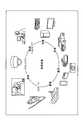
- FIG. 22 is a diagram illustrating a usage example of the imaging device 1 according to the present disclosure described above.
- the above-described imaging device can be used in various cases for sensing light such as visible light, infrared light, ultraviolet light, and X-ray as described below.
- a device for photographing an image provided for viewing such as a digital camera or a portable device having a photographing function.
- In-vehicle sensors that capture images of the front, back, surroundings, and the inside of the vehicle, monitoring cameras that monitor running vehicles and roads, inter-vehicle, etc. for safe driving such as automatic stop and recognition of the driver's condition
- a device used for traffic such as a distance measuring sensor that measures the distance of a vehicle.
- a device provided to home appliances such as a TV, a refrigerator, and an air conditioner for photographing a user's gesture and performing device operation according to the gesture.
- -Devices used for medical or health care such as endoscopes and devices that perform blood vessel imaging by receiving infrared light.
- Devices used for security such as surveillance cameras for crime prevention and cameras for person authentication.
- -Apparatus used for beauty such as a skin measuring instrument for photographing the skin and a microscope for photographing the scalp.
- -Equipment used for sports such as action cameras and wearable cameras for sports applications.
- Devices used for agriculture such as cameras for monitoring the condition of fields and crops.
- a control unit that outputs the third control signal to the third signal line, and outputs the third control signal to the third signal line.
- a solid-state imaging device comprising: (2) The control unit includes: Outputting, to the second signal line, a second control signal for causing the holding unit to hold a pixel signal read from the first pixel to the vertical signal line; The solid according to (1), wherein when reading out a pixel signal from the second pixel, the third control signal for reading out the pixel signal held in the holding unit is output to the third signal line. Imaging device. (3) The control unit includes: When reading a pixel signal from the second pixel, the P-phase output and the D-phase output included in the pixel signal held in the holding unit are used to output the D-phase output to the vertical signal line.
- the solid-state imaging device which outputs a third control signal to the third signal line.
- the control unit includes: When reading out a pixel signal from the second pixel, among the P-phase output and the D-phase output included in the pixel signal stored in the holding unit, the P-phase output is output to the vertical signal line.
- the solid-state imaging device which outputs a third control signal to the third signal line.
- the third control signal for outputting a P-phase output and a D-phase output included in the pixel signal stored in the holding unit to the vertical signal line is provided.
- the solid-state imaging device which outputs the signal to the third signal line.
- the second pixel is The solid according to any one of (1) to (5), which is arranged at another position in the set corresponding to the position of the color in which the first pixel is arranged in the set based on the arrangement of the plurality of colors.
- the first pixel is Converting the received light into a first signal for an image and outputting it as a pixel signal;
- the second pixel is The solid-state imaging device according to any one of (1) to (6), wherein the received light is converted into a second signal having a function different from that of the first signal and output as a pixel signal.
- the solid-state imaging device according to any one of (1) to (7), further including a buffer unit using a voltage follower amplifier connected between the holding unit and the vertical signal line.
- a control unit that outputs the third control signal to the third signal line, and outputs the third control signal to the third signal line.
- An output unit that performs image processing on a pixel signal read from the first pixel and the second pixel via the vertical signal line and outputs the processed pixel signal; Electronic equipment provided with.
- the control unit includes: Outputting, to the second signal line, a second control signal for causing the holding unit to hold a pixel signal read from the first pixel to the vertical signal line;
- the electronic device according to (10), wherein, when a pixel signal is read from the second pixel, the third control signal for reading the pixel signal held in the holding unit is output to the third signal line. machine.
- the control unit includes: When reading a pixel signal from the second pixel, the P-phase output and the D-phase output included in the pixel signal held in the holding unit are used to output the D-phase output to the vertical signal line.
- the control unit includes: When reading out a pixel signal from the second pixel, among the P-phase output and the D-phase output included in the pixel signal stored in the holding unit, the P-phase output is output to the vertical signal line.
- the third control signal for outputting a P-phase output and a D-phase output included in the pixel signal stored in the holding unit to the vertical signal line is provided.
- the second pixel is The electronic device according to any one of (10) to (14), which is arranged at another set position corresponding to the color position at which the first pixel is arranged in the set based on the arrangement of the plurality of colors. machine.
- the first pixel is Converting the received light into a first signal for an image and outputting it as a pixel signal
- the second pixel is The electronic device according to any one of (10) to (15), wherein the received light is converted into a second signal having a function different from that of the first signal and output as a pixel signal.
- the electronic device according to any one of (10) to (16) further including a buffer unit using a voltage follower amplifier connected between the holding unit and the vertical signal line.
- One of the pixel signal held in the holding unit and a signal of a predetermined voltage supplied from the outside is switched so as to be supplied to a buffer unit connected between the holding unit and the vertical signal line.
Landscapes
- Engineering & Computer Science (AREA)
- Multimedia (AREA)
- Signal Processing (AREA)
- Transforming Light Signals Into Electric Signals (AREA)
- Solid State Image Pick-Up Elements (AREA)
Abstract
La présente invention comprend : des premiers et seconds pixels (31, 41) qui sont connectés à une ligne de signal vertical (17); une unité de maintien (501) qui est connectée à la ligne de signal vertical et maintient un signal de pixel apparaissant sur la ligne de signal verticale; une première ligne de signal (16) qui est connectée aux premiers et seconds pixels et auquel un premier signal de commande pour commander la lecture d'un signal de pixel vers la ligne de signal verticale est entré à partir des premiers et seconds pixels; des deuxièmes lignes de signal (185, 186) qui sont connectées à l'unité de maintien et auxquelles un second signal de commande pour maintenir le signal de pixel lu sur la ligne de signal verticale dans l'unité de maintien est entré; des troisièmes lignes de signal (183, 184) qui sont connectées à l'unité de maintien et auxquelles un troisième signal de commande pour commander la lecture des signaux de pixel maintenus par l'unité de maintien sur la ligne de signal verticale est entré; et une unité de commande (19) qui est connectée aux première à troisième lignes de signal et délivre les premier à troisième signaux de commande aux première à troisième lignes de signal, respectivement.
Applications Claiming Priority (2)
| Application Number | Priority Date | Filing Date | Title |
|---|---|---|---|
| JP2018156686A JP2020031371A (ja) | 2018-08-23 | 2018-08-23 | 固体撮像素子および電子機器 |
| JP2018-156686 | 2018-08-23 |
Publications (1)
| Publication Number | Publication Date |
|---|---|
| WO2020039909A1 true WO2020039909A1 (fr) | 2020-02-27 |
Family
ID=69591963
Family Applications (1)
| Application Number | Title | Priority Date | Filing Date |
|---|---|---|---|
| PCT/JP2019/030784 Ceased WO2020039909A1 (fr) | 2018-08-23 | 2019-08-05 | Élément d'imagerie à semi-conducteurs et dispositif électronique |
Country Status (2)
| Country | Link |
|---|---|
| JP (1) | JP2020031371A (fr) |
| WO (1) | WO2020039909A1 (fr) |
Families Citing this family (1)
| Publication number | Priority date | Publication date | Assignee | Title |
|---|---|---|---|---|
| JP2022144242A (ja) * | 2021-03-18 | 2022-10-03 | キヤノン株式会社 | 光電変換装置、光電変換システムおよび移動体 |
Citations (5)
| Publication number | Priority date | Publication date | Assignee | Title |
|---|---|---|---|---|
| JP2008252605A (ja) * | 2007-03-30 | 2008-10-16 | Sony Corp | 固体撮像装置、固体撮像装置の信号処理方法および撮像装置 |
| JP2010130398A (ja) * | 2008-11-28 | 2010-06-10 | Sony Corp | 固体撮像装置、固体撮像装置の駆動方法および撮像装置 |
| JP2014239289A (ja) * | 2013-06-06 | 2014-12-18 | ソニー株式会社 | Ad変換器、信号処理方法、固体撮像装置、および電子機器 |
| JP2016082453A (ja) * | 2014-10-17 | 2016-05-16 | キヤノン株式会社 | 固体撮像装置及びその駆動方法、並びに、撮像システム |
| JP2016213740A (ja) * | 2015-05-12 | 2016-12-15 | キヤノン株式会社 | 撮像装置及び撮像システム |
-
2018
- 2018-08-23 JP JP2018156686A patent/JP2020031371A/ja active Pending
-
2019
- 2019-08-05 WO PCT/JP2019/030784 patent/WO2020039909A1/fr not_active Ceased
Patent Citations (5)
| Publication number | Priority date | Publication date | Assignee | Title |
|---|---|---|---|---|
| JP2008252605A (ja) * | 2007-03-30 | 2008-10-16 | Sony Corp | 固体撮像装置、固体撮像装置の信号処理方法および撮像装置 |
| JP2010130398A (ja) * | 2008-11-28 | 2010-06-10 | Sony Corp | 固体撮像装置、固体撮像装置の駆動方法および撮像装置 |
| JP2014239289A (ja) * | 2013-06-06 | 2014-12-18 | ソニー株式会社 | Ad変換器、信号処理方法、固体撮像装置、および電子機器 |
| JP2016082453A (ja) * | 2014-10-17 | 2016-05-16 | キヤノン株式会社 | 固体撮像装置及びその駆動方法、並びに、撮像システム |
| JP2016213740A (ja) * | 2015-05-12 | 2016-12-15 | キヤノン株式会社 | 撮像装置及び撮像システム |
Also Published As
| Publication number | Publication date |
|---|---|
| JP2020031371A (ja) | 2020-02-27 |
Similar Documents
| Publication | Publication Date | Title |
|---|---|---|
| US11050955B2 (en) | Solid-state imaging device, method for driving solid-state imaging device, and electronic apparatus | |
| US9185318B2 (en) | Solid-state imaging device, signal processing method of solid-state imaging device, and electronic apparatus | |
| US6914227B2 (en) | Image sensing apparatus capable of outputting image by converting resolution by adding and reading out a plurality of pixels, its control method, and image sensing system | |
| US9807330B2 (en) | Solid-state imaging device and imaging apparatus | |
| US10567687B2 (en) | Solid state imaging device and electronic apparatus for removing a noise component | |
| CN107408566B (zh) | 固态成像设备和电子装置 | |
| JP2004297546A (ja) | 撮像装置 | |
| CN103634538A (zh) | 图像感测装置 | |
| CN105407299B (zh) | 摄像装置及控制摄像装置的方法 | |
| WO2018012088A1 (fr) | Élément d'imagerie à semi-conducteurs et procédé de commande d'élément d'imagerie à semi-conducteurs | |
| WO2020022120A1 (fr) | Circuit de correction de traînage, dispositif de capture d'image, et appareil électronique | |
| WO2020039909A1 (fr) | Élément d'imagerie à semi-conducteurs et dispositif électronique | |
| US12513430B2 (en) | Solid-state imaging device, method for driving the same, and electronic device for simultaneously reading signal levels of different capacitive elements | |
| WO2012023271A1 (fr) | Dispositif de capture d'image | |
| US7999871B2 (en) | Solid-state imaging apparatus, and video camera and digital still camera using the same | |
| JP7271131B2 (ja) | 撮像装置および撮像装置の制御方法 | |
| WO2019216029A1 (fr) | Dispositif d'imagerie, appareil électronique, et procédé d'entraînement | |
| US20260129320A1 (en) | Solid-state imaging device and driving method thereof, and electronic apparatus | |
| JP6393087B2 (ja) | 撮像素子及び撮像装置 | |
| JP2017220949A (ja) | 撮像装置 | |
| WO2024084930A1 (fr) | Dispositif d'imagerie à semi-conducteurs, son procédé de commande, et équipement électronique | |
| TWI429281B (zh) | 固態成像裝置,固態成像裝置之信號處理方法,及電子設備 | |
| WO2017187975A1 (fr) | Élément d'imagerie à semi-conducteurs, procédé de pilotage et dispositif électronique | |
| JP2018125594A (ja) | 撮像装置 |
Legal Events
| Date | Code | Title | Description |
|---|---|---|---|
| 121 | Ep: the epo has been informed by wipo that ep was designated in this application |
Ref document number: 19852835 Country of ref document: EP Kind code of ref document: A1 |
|
| NENP | Non-entry into the national phase |
Ref country code: DE |
|
| 122 | Ep: pct application non-entry in european phase |
Ref document number: 19852835 Country of ref document: EP Kind code of ref document: A1 |