WO2020042829A1 - 感光组件、摄像模组及其制作方法 - Google Patents
感光组件、摄像模组及其制作方法 Download PDFInfo
- Publication number
- WO2020042829A1 WO2020042829A1 PCT/CN2019/097078 CN2019097078W WO2020042829A1 WO 2020042829 A1 WO2020042829 A1 WO 2020042829A1 CN 2019097078 W CN2019097078 W CN 2019097078W WO 2020042829 A1 WO2020042829 A1 WO 2020042829A1
- Authority
- WO
- WIPO (PCT)
- Prior art keywords
- photosensitive
- chip
- layer
- photosensitive chip
- circuit board
- Prior art date
- Legal status (The legal status is an assumption and is not a legal conclusion. Google has not performed a legal analysis and makes no representation as to the accuracy of the status listed.)
- Ceased
Links
Images


Classifications
-
- H—ELECTRICITY
- H04—ELECTRIC COMMUNICATION TECHNIQUE
- H04N—PICTORIAL COMMUNICATION, e.g. TELEVISION
- H04N23/00—Cameras or camera modules comprising electronic image sensors; Control thereof
- H04N23/50—Constructional details
- H04N23/54—Mounting of pick-up tubes, electronic image sensors, deviation or focusing coils
-
- H—ELECTRICITY
- H04—ELECTRIC COMMUNICATION TECHNIQUE
- H04N—PICTORIAL COMMUNICATION, e.g. TELEVISION
- H04N23/00—Cameras or camera modules comprising electronic image sensors; Control thereof
- H04N23/57—Mechanical or electrical details of cameras or camera modules specially adapted for being embedded in other devices
-
- H—ELECTRICITY
- H10—SEMICONDUCTOR DEVICES; ELECTRIC SOLID-STATE DEVICES NOT OTHERWISE PROVIDED FOR
- H10F—INORGANIC SEMICONDUCTOR DEVICES SENSITIVE TO INFRARED RADIATION, LIGHT, ELECTROMAGNETIC RADIATION OF SHORTER WAVELENGTH OR CORPUSCULAR RADIATION
- H10F39/00—Integrated devices, or assemblies of multiple devices, comprising at least one element covered by group H10F30/00, e.g. radiation detectors comprising photodiode arrays
- H10F39/10—Integrated devices
- H10F39/12—Image sensors
-
- H—ELECTRICITY
- H10—SEMICONDUCTOR DEVICES; ELECTRIC SOLID-STATE DEVICES NOT OTHERWISE PROVIDED FOR
- H10F—INORGANIC SEMICONDUCTOR DEVICES SENSITIVE TO INFRARED RADIATION, LIGHT, ELECTROMAGNETIC RADIATION OF SHORTER WAVELENGTH OR CORPUSCULAR RADIATION
- H10F39/00—Integrated devices, or assemblies of multiple devices, comprising at least one element covered by group H10F30/00, e.g. radiation detectors comprising photodiode arrays
- H10F39/80—Constructional details of image sensors
- H10F39/811—Interconnections
Definitions
- the present application relates to the field of optical technology, and in particular, the present application relates to a photosensitive component, a camera module, and a manufacturing method thereof.
- the camera module usually includes an optical lens component and a photosensitive component.
- the photosensitive component generally includes a circuit board and a photosensitive chip 103 mounted on the circuit board.
- the photosensitive chip 103 is usually connected to the circuit layer through a "gold wire” (ie wire bonding or wire bonding) process or a flip chip (ie flip chip) process.
- the gold wire has a certain arc height. Therefore, in order to avoid the gold wire in the module, an extra height is usually added. Therefore, the existence of the gold wire may hinder the miniaturization of the module.
- the flip chip process uses the flip chip process to solve a series of problems brought about by gold wires.
- the flip chip process since the chip is directly attached to the bottom side of the circuit board, and then the chip and the circuit board are connected by a gold ball, the conduction length of the circuit board and the photosensitive chip is greatly shortened in this process. Reduced delay and effectively improved electrical performance.
- the Flip Chip process has high requirements for conduction accuracy and flatness, and it is necessary to use a ceramic substrate with high structural strength and not easy to bend as a circuit board (ie, a circuit board), and its price is very expensive.
- this process solution requires that the pad size and pad density of the circuit board be the same or substantially the same as the pad size and pad density of the photosensitive chip.
- the minimum size of the pads of the circuit board is limited, and the gold ball bump line width is large, such as about 100um.
- the number of pads that can be arranged on the photosensitive chip is reduced, or increasing the number of pads will increase the size of the photosensitive chip, which is not conducive to reducing the size of the camera module.
- the higher the number of pixels of the photosensitive chip the larger the amount of image data that needs to be output, and more I / O ports are required to output data.
- the smaller number of pads results in fewer I / O ports for output data. Therefore, the existing flip chip process is not conducive to increasing the number of pixels of the photosensitive chip.
- the present application provides a solution capable of overcoming at least one drawback of the prior art.
- a photosensitive component including: a photosensitive chip having a photosensitive region and a non-photosensitive region surrounding the photosensitive region, wherein the non-photosensitive region is provided with a plurality of chip electrodes; A layer located on a side of the photosensitive chip and in contact with the photosensitive chip, and having a surface flush with a front surface of the photosensitive chip; and a rewiring layer formed on the extension layer and the photosensitive chip Front side; the redistribution layer has a plurality of redistribution layer electrodes, and the plurality of redistribution layer electrodes are in one-to-one correspondence with the plurality of chip electrodes through the redistribution layer traces and are turned on.
- the circuit board further includes a plurality of circuit board electrodes, and the plurality of redistribution layer electrodes are in one-to-one correspondence with and connected to the plurality of circuit board electrodes.
- the circuit board is a rigid-soft board.
- a central region of the circuit board and a central region of the redistribution layer have through holes, and the chip electrode is closer to the through hole than the redistribution layer electrode.
- the wiring board and the rewiring layer have a filling material around the attachment position.
- An area of the chip electrode is smaller than an area of the rewiring layer electrode.
- the density of the plurality of chip electrodes is higher than the density of the plurality of redistribution layer electrodes; the width of the redistribution layer traces is smaller than the width of the traces of the circuit board.
- the extension layer surrounds the photosensitive chip, or is located on one side, two sides, or three sides of the photosensitive chip.
- the back of the circuit board has a groove, and the photosensitive chip is located in the groove.
- the photosensitive component further includes a metal sheet attached to the circuit board and covering the groove.
- the photosensitive component further includes a metal sheet attached to the circuit board and covering a back surface of the photosensitive chip, and the metal sheet has a groove and the photosensitive chip is located in the groove Inside.
- a gap is left between the metal sheet and the photosensitive chip.
- the photosensitive component further includes a molding layer, and the molding layer covers a back surface of the circuit board and the photosensitive chip.
- the photosensitive chip has a row of chip electrodes on the top or bottom side, and the chip electrodes are connected to the left or right side of the photosensitive chip through the rewiring layer traces. Re-route the layer electrodes.
- the surface of the photosensitive region of the photosensitive chip has a protective layer; the protective layer is a color filter or a transparent cover.
- a camera module including: any one of the foregoing photosensitive components; and an optical lens component mounted on the photosensitive component.
- a method for manufacturing a photosensitive component includes: placing a photosensitive chip on a surface of a substrate; and forming an extension layer extending from a side of the photosensitive chip on the surface of the substrate and making the extension The surface of the layer is flush with the surface of the photosensitive chip; and a rewiring layer is made on the flush surface of the extension layer and the photosensitive chip, and a plurality of photosensitive electrodes of the photosensitive chip are routed through the rewiring layer It is connected to a plurality of redistribution layer electrodes located on the redistribution layer, and the size and layout of the plurality of redistribution layer electrodes are adapted to attach a plurality of circuit board electrodes one-to-one correspondingly.
- the photosensitive surface of the photosensitive chip faces the substrate; and in the step of making an extension layer extending from the side of the photosensitive chip on the surface of the substrate, The contact surface between the extension layer and the substrate and the surface of the photosensitive chip on the photosensitive surface side constitute the flush surface for making the rewiring layer.
- molding is performed from the back of the photosensitive chip to form a molding portion surrounding the photosensitive chip, and the molding portion As the extension layer.
- the step of making an extension layer extending from the side of the photosensitive chip on the surface of the substrate further comprises: grinding the extension layer to thin the photosensitive component.
- the step of fabricating an extension layer extending from the side of the photosensitive chip on the surface of the substrate further comprises: grinding the extension layer and the back surface of the photosensitive chip to thin the photosensitive component.
- the step of preparing a redistribution layer on a flush surface of the extension layer and the photosensitive chip further includes: removing the redistribution layer covering the photosensitive surface of the photosensitive chip to expose the photosensitive surface.
- the method for manufacturing a photosensitive component further comprises: forming a protective layer on the photosensitive surface of the photosensitive chip before the step of preparing a rewiring layer on the flush surface of the extension layer and the photosensitive chip.
- the protective layer is a sacrificial layer
- the method for manufacturing the photosensitive component further includes: manufacturing a rewiring layer on a flush surface of the extension layer and the photosensitive chip. After the step is completed, the sacrificial layer is removed.
- the protective layer is a color filter.
- the method for manufacturing a photosensitive component further includes: attaching a circuit board to the redistribution layer after the step of preparing a redistribution layer on a flush surface of the expansion layer and the photosensitive chip, the multi-layer
- Each of the redistribution layer electrodes is in one-to-one correspondence with a plurality of circuit board electrodes of the circuit board and is conductive.
- the method for manufacturing a photosensitive component further comprises: after attaching a circuit board to the re-routing layer, attaching a metal sheet to the back of the circuit board, so that the metal sheet covers the back of the photosensitive chip.
- the method for manufacturing a photosensitive component further includes: after attaching a circuit board to the redistribution layer, arranging a filling material around the attachment position of the circuit board and the redistribution layer; The back of the circuit board and the photosensitive chip is covered with a molding layer.
- a plurality of the photosensitive chips are arranged at intervals on the surface of the same substrate to form a photosensitive chip array; the step of making an expansion layer surrounding the photosensitive chip on the substrate surface
- an integrally formed extension layer is fabricated on the substrate, and the extension layer surrounds each photosensitive chip to form an array of photosensitive chip components.
- step of preparing a rewiring layer on the flush surface of the extension layer and the photosensitive chip Fabricating the rewiring layer on the surface of the photosensitive chip component array; and after performing the step of making a rewiring layer on the flush surface of the expansion layer and the photosensitive chip, cutting the photosensitive chip component array, To obtain a single photosensitive member.
- the photosensitive chip component array is cut from the back.
- the present application can realize the connection of the circuit board pads / circuits with larger line widths to the light-sensitive chips with smaller contacts, and realize the high-density packaging of the light-sensitive chips of the camera module.
- the present application can realize that the circuit board pads relatively close to the outside of the light window are conducted to the chip pads closer to the light window.
- the present application can realize that the camera module uses a conventional printed circuit board to implement a flip chip process, so as to achieve a high I / O number package.
- FIG. 1 is a schematic cross-sectional view of a photosensitive component according to an embodiment of the present application
- FIG. 2 is a schematic top view of the photosensitive component shown in FIG. 1; FIG.
- FIG. 3 is a schematic top view of a photosensitive component according to another embodiment of the present application.
- FIG. 4 shows a schematic diagram of placing the photosensitive chip 103 on the substrate 105a
- FIG. 5 shows a placement manner of a photosensitive chip array adapted to a wafer level process
- FIG. 6 shows a placement manner of a photosensitive chip array adapted to a panel level process
- FIG. 8 shows the components of the molded part 109 and the photosensitive chip 103 after grinding
- FIG. 9 shows a schematic diagram of forming a rewiring layer on the front surface of the photosensitive chip 103 and the surface of the molding part 109 around it;
- FIG. 10 shows a schematic diagram of forming a light window 106
- FIG. 11 shows a schematic diagram of cutting a photosensitive chip component array
- FIG. 12 shows a schematic diagram of attaching a photosensitive chip assembly to the circuit board 101
- FIG. 13 shows a schematic diagram of attaching a metal sheet 104 on the surface (usually the back surface) of the circuit board 101 to cover the back of the photosensitive chip 103;
- FIG. 14 shows a schematic diagram of molding on the back of the circuit board 101 and the photosensitive chip assembly
- FIG. 15 is a schematic diagram of a photosensitive component according to another embodiment of the present application.
- FIG. 16 shows a molded photosensitive chip array with a protective layer 110 in an embodiment of the present application
- FIG. 17 shows a schematic diagram of forming a rewiring layer 102 on the front surface of the photosensitive chip 103 and the surface of the molding part 109 around it in step S400 ';
- FIG. 18 shows a photosensitive chip component array after removing the protective layer 110
- FIG. 19 shows a schematic diagram of cutting a photosensitive chip module array with a protective layer
- FIG. 20 shows a schematic diagram of a photosensitive chip assembly with a protective layer attached to the circuit board 101;
- FIG. 21 shows a schematic view of a photosensitive member to which a protective layer of a metal sheet 104 is attached
- FIG. 22 shows a schematic diagram of molding on the backside of the circuit board 101 and the photosensitive chip assembly retaining the photosensitive protective layer;
- FIG. 23 is a schematic diagram of a photosensitive component retaining a photosensitive protective layer according to another embodiment of the present application.
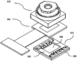
- FIG. 24 is a schematic three-dimensional explosion diagram of a camera module according to an embodiment of the present application.
- FIG. 25 is a schematic three-dimensional explosion diagram of the photosensitive chip assembly 113.
- the expressions of the first, second, etc. are only used to distinguish one feature from another feature, and do not indicate any limitation on the feature. Therefore, without departing from the teachings of this application, the first subject discussed below may also be referred to as the second subject.
- FIG. 1 is a schematic cross-sectional view of a photosensitive component according to an embodiment of the present application.
- the photosensitive component includes a photosensitive chip 103, a molding portion 109, a rewiring layer 102, and a circuit board 101.
- the lower surface of the wiring board 101 has a plurality of wiring board electrodes 1014 (ie, first electrodes).
- the photosensitive chip 103 includes a photosensitive region 1031 and a non-photosensitive region 1032 surrounding the photosensitive region 1031.
- the chip electrode 1033 is provided in the non-photosensitive area 1032.
- the molding portion 109 is formed around the photosensitive chip 103, and the upper surface of the molding portion 109 is flush with the upper surface of the photosensitive chip 103 to form an overall flat surface.
- the rewiring layer 102 is formed on a flat surface.
- the upper surface of the redistribution layer 102 has a plurality of redistribution layer electrodes 1022 (ie, second electrodes) corresponding to the plurality of circuit board electrodes 1014, and each redistribution layer electrode 1022 corresponds to The chip electrode 1033 is in communication.
- the wiring board has a through-hole 1013 as a light-through hole in the center.
- the circuit board 101 may be a rigid-soft board.
- the rigid-soft board includes a hard-board area 1011 and a soft-board area 1012.
- the hard-board area 1011 has a through hole 1013 in the center.
- the hard board area can be understood as a region where the whole of the rigid-flex board is rigid (inflexible at normal temperature), and the soft board area can be understood as the whole of the rigid-flex board which is flexible (i.e. (Bent).
- the rigid board region may be a region that is rigid as a whole formed by laminating a plurality of rigid boards and a flexible board, and does not necessarily consist of only a rigid board.
- FIG. 2 shows a schematic top view of the photosensitive component shown in FIG. 1.
- This figure is a perspective view, and the wiring board is omitted.
- the figure shows the redistribution layer electrode 1022, the chip electrode 1033, and the redistribution layer wiring 1023.
- the redistribution layer trace 1023 connects and conducts the redistribution layer electrode 1022 and the chip electrode 1033.
- the area of the rewiring layer electrode 1022 may be larger than the area of the chip electrode 1033.
- the area of the redistribution layer electrode 1022 matches the area of the circuit board electrode 1014 (for example, is equal or substantially equal).
- the redistribution layer electrode 1022 is located outside the chip electrode 1033 (that is, the chip electrode 1033 is closer to the physical center of the through hole 1013 than the redistribution layer electrode 1022).
- the electrodes may be all metal electrodes.
- the pad size range of the rigid-flex board is 60 to 80 m, and the pad size of the chip can be 10 to 20 m. Therefore, in the above embodiment, a fan-out package is implemented by forming an expansion layer (such as a molding part 109) around the photosensitive chip 103, and then forming a rewiring layer 102 on the flat surface of the photosensitive chip 103 on the common surface of the expansion layer.
- the photosensitive chip assembly composed of the photosensitive chip 103, the expansion layer, and the redistribution layer 102 may have pads suitable for being assembled with a circuit board by flip-chip assembly. The size and layout of these pads can be adapted one-to-one with the circuit board electrodes (ie, circuit board pads).
- the chip electrodes of the photosensitive chips still have the characteristics of small area and dense arrangement, thereby helping to increase the number of pixels of the photosensitive components of the filp chip process scheme, while avoiding the existing wire bonding process. Bring various defects.
- the soft-hard board is a flexible circuit board (soft board) and a rigid circuit board (hard board). After pressing and other processes, they are combined according to relevant process requirements to form an FPC and PCB circuit board. At present, the manufacturing process of flexible and rigid boards has been relatively mature, and it has a large cost advantage compared to other processes such as ceramic substrates.
- connection belt of the photosensitive component in the above embodiment is made by using a manufacturing process of a rigid-flexible board, which can avoid attaching the connection belt after attaching the photosensitive chip through a process that requires high temperature hot pressing such as ACF.
- the connecting strip can electrically connect the hard board area to the connector so as to be electrically connected to the main board of a terminal device (such as a mobile phone).
- the flexible board of the rigid-flex board can be directly used as the connection belt of the photosensitive component.
- the flexible board region extends to the rigid board region through the side of the rigid board region. Based on the ACF process, the connecting strip connects the hard board through the hard board surface (usually the edge area of the hard board surface).
- the photosensitive component includes a photosensitive chip and a circuit board.
- the circuit board has a through hole corresponding to the photosensitive region of the photosensitive chip.
- the optical axis of the photosensitive chip overlaps the physical centerline of the through hole or has only a small deviation.
- the distance between the first pad on the lower surface of the circuit board and the physical center of the via is far.
- the attachment of the photosensitive chip 103 and the circuit board 101 is achieved by other processes without increasing the distance from the chip electrode 1033 (the chip electrode may be a chip pad) to the physical center of the through hole 1013. Connect and conduct.
- the photosensitive component includes a photosensitive chip component, a circuit board 101, and a rewiring layer 102.
- the photosensitive chip component includes a photosensitive chip 103 and an expansion layer extending on both sides of the photosensitive chip 103.
- the chip 103 has a photosensitive region and a non-photosensitive region surrounding the photosensitive region.
- the non-photosensitive region is provided with a plurality of chip electrodes 1033.
- the expansion layer extends from the non-photosensitive area to the peripheral side, so that the length and width dimensions of the photosensitive chip component are expanded relative to the size of the photosensitive chip 103.
- the extension layer is formed by, but not limited to, a photolithography process, a molding process, and the like.
- the circuit board electrode 1014 When the circuit board electrode 1014 is projected (orthographic) on the upper surface of the photosensitive chip assembly along the optical axis direction of the photosensitive chip 103 (or the direction perpendicular to the photosensitive surface of the photosensitive chip 103), the circuit board electrode 1014 is projected outside the chip electrode 1033. Or the orthographic projection of the circuit board electrode 1014 along the optical axis direction of the photosensitive chip 103 is located in the extension layer.
- the expansion layer is not limited to extend from the non-photosensitive region to the peripheral side, for example, in other embodiments, it may extend from the non-photosensitive region to three sides, two sides, or even one side.
- FIG. 3 shows a schematic top view of a photosensitive component according to another embodiment of the present application.
- This figure is a perspective view, and the wiring board is omitted, and the redistribution layer electrode 1022 and the chip electrode 1033 are shown in the figure.
- the redistribution layer trace 1023 is not shown in FIG. 3.
- the redistribution layer wiring 1023 connects the redistribution layer electrode 1022 and the chip electrode 1033.
- an area of the rewiring layer electrode 1022 may be larger than an area of the chip electrode 1033.
- the area of the redistribution layer electrode 1022 matches the area of the circuit board electrode 1014 (for example, is equal or substantially equal).
- the redistribution layer electrode 1022 is located outside the chip electrode 1033 (that is, the chip electrode 1033 is closer to the physical center of the through hole 1013 than the redistribution layer electrode 1022).
- the electrodes may be all metal electrodes.
- the chip electrodes 1033 provided on the top side of the photosensitive chip 103 can be led to the left and right sides, so that the size in the Y direction is not increased too much. In FIG. 3, the direction from bottom to top is the Y direction, and the direction from right to left is the X direction.
- the chip pad and the rewiring layer pad may partially overlap. For clarity, the overlap is not shown in Figure 3.
- the redistribution layer electrodes 1022 on each side may have multiple rows so that more electrodes are arranged on the same side (eg, left or right) of the photosensitive chip.
- the chip 1033 electrode on the top side of the photosensitive chip is led to the left and right sides by the redistribution layer wiring to connect the left and right redistribution layer electrodes 1022.
- the size in the layer Y direction ie, the direction from bottom to top in FIG. 3) is reduced. It should be noted that for the sake of clarity, Figure 3 does not show the re-routing layer traces.
- the photosensitive component may further include a metal sheet 104.
- the metal sheet 104 has a groove 104a, and the photosensitive chip is received in the groove 104a. After attaching the metal sheet, you can get a complete photosensitive assembly.
- the metal sheet 104 is attached to the back of the redistribution layer 102, which can isolate the photosensitive chip 103 from the external environment and prevent the photosensitive chip 103 from being damaged by external force.
- a reserved gap can be maintained between the metal sheet 104 and the photosensitive chip 103, so as to prevent collision between the metal sheet 104 and the photosensitive chip 103 and cause damage to the photosensitive chip 103 or electrical connection failure.
- the gap can be filled with air, glue, molding, insulation, etc. to better protect the chip.
- FIG. 4-13 illustrates a manufacturing process of a photosensitive component according to an embodiment of the present application.
- the method for manufacturing a photosensitive component includes the following steps.
- the photosensitive chip 103 is placed on a substrate 105a (also referred to as a carrier board), wherein the photosensitive surface of the photosensitive chip 103 faces downward, that is, the photosensitive chip 103 is buckled on the substrate 105a.
- FIG. 4 shows a schematic diagram of placing the photosensitive chip 103 on the substrate 105a.
- a plurality of photosensitive chips 103 may be arranged on the substrate 105a at a certain pitch.
- the layout can be shown in Figure 5.
- FIG. 5 shows the arrangement of the photosensitive chip array adapted to the wafer level process.
- the arrangement manner of the photosensitive chip array may also be a placement manner adapted to a panel level process.
- FIG. 6 shows a photosensitive chip array placement method adapted to a panel level process.
- a molding portion 109 is formed on the substrate surface and the backside of the photosensitive chip to cover the photosensitive chip, thereby combining the photosensitive chip 103, the molding portion 109, and the substrate 105a together.
- FIG. 7 shows a schematic view of molding on the substrate surface and the backside of the photosensitive chip.
- FIG. 8 shows the components of the molded part 109 and the photosensitive chip 103 after grinding.
- the photosensitive chip 103 used is usually ground (thickness before grinding is 0.3 mm or more, and after grinding is 0.15 mm). In this embodiment, if a wafer having a thickness of 0.15 mm is used for wafer / panel level molding, warping may be caused. When the number of the photosensitive chips 103 molded at one time is large, the warpage is very large.
- step S300 is an optional step. In some embodiments of the present application, step S300 may be omitted.
- FIG. 9 is a schematic diagram showing the formation of a rewiring layer on the front surface of the photosensitive chip 103 and the surface of the molding part 109 around it.
- the substrate 105a that is, the substrate of step S100
- the molded photosensitive chip array may be peeled off first, and then the molded photosensitive chip array is placed on the other substrate 105b with the front side facing up, and then the photosensitive chip array
- a redistribution layer is formed on the front surface of 103 and the surface of the molding portion 109 around it.
- the surface of the formed redistribution layer 102 has a redistribution layer electrode 1022, and the redistribution layer electrode 1022 is connected to the chip electrode 1033 through a redistribution layer trace 1023.
- the size of the redistribution layer electrode 1022 may be larger than the size of the chip electrode 1033, and the position of the redistribution layer electrode 1022 may be located outside the chip electrode 1033 (that is, a position farther from the photosensitive center). In this embodiment, the entire redistribution layer electrode 1022 is located above the molding portion 109.
- a part of the redistribution layer electrode may be located above the molding part 109 and another part may be located above the photosensitive chip 103, and even the redistribution layer electrode 1022 may have a partial overlap with the chip electrode 1033 (that is, the redistribution layer electrode) A part of 1022 may be located above the chip electrode 1033).
- the rewiring layer 102 can be fabricated on the front surfaces of the components of the molding part 109 and the photosensitive chip 103 based on the photoresist spin coating, exposure, development, and plating processes.
- the rewiring layer may include a dielectric layer.
- the redistribution layer trace 1023 is embedded in the dielectric layer.
- FIG. 10 shows a schematic diagram of forming the light window 106.
- step S400 no rewiring layer traces 1023 are provided above the photosensitive region 1031 of the photosensitive chip 103. Therefore, the rewiring layer 102 above the photosensitive region 1031 is actually a dielectric layer. By removing the dielectric layer above the photosensitive area 1031, a photosensitive chip component with a light window can be obtained.
- This photosensitive chip module is composed of a photosensitive chip 103, a molding part 109, and a rewiring layer 102. It should be noted that when multiple photosensitive chips 103 are molded at the same time, what is obtained in this step is an array of photosensitive chip components.
- FIG. 11 shows a schematic diagram of cutting the photosensitive chip module array.
- the cutting is preferably performed from the back surface 111. This prevents the chip from being contaminated on the one hand, and facilitates the subsequent pickup and attachment of the chip assembly to the circuit board on the other.
- the substrate on the back of the photosensitive chip component array may be peeled off first, and then the photosensitive chip component array is placed face down on another substrate, and then cut from the back of the photosensitive chip component array.
- FIG. 12 shows a schematic diagram of attaching the photosensitive chip assembly to the circuit board 101. This attachment is achieved based on a flip chip process. As shown in FIG. 12, the redistribution layer electrode 1022 and the circuit board electrode 1014 of the photosensitive chip assembly are in one-to-one correspondence and are in conduction.
- FIG. 13 shows a schematic diagram of attaching a metal sheet 104 on the surface (usually the back surface) of the circuit board 101 to cover the back of the photosensitive chip 103.
- the metal sheet 104 has a groove 104a, and the photosensitive chip 103 is received in the groove 104a. After the metal sheet 104 is attached, a complete photosensitive component can be obtained.
- the metal sheet 104 is attached to the back of the redistribution layer 102, which can isolate the photosensitive chip 103 from the external environment and prevent the photosensitive chip 103 from being damaged by external force.
- a reserved gap can be maintained between the metal sheet 104 and the photosensitive chip 103, so as to prevent collision between the metal sheet 104 and the photosensitive chip 103 and cause damage to the photosensitive chip 103 or electrical connection failure.
- the gap can be filled with air, glue, molding, insulation, etc. to better protect the chip.
- FIG. 14 shows a schematic view of molding on the backside of the circuit board 101 and the photosensitive chip module.
- the metal sheet 104 may be replaced by the molding layer 107.
- the molding layer 107 may be formed on the back surface of the redistribution layer 102 and the back surface of the photosensitive chip 103 by a molding process.
- the gap between the redistribution layer 102 and the circuit board 103 (mainly the area around the connection point of the redistribution layer electrode 1022 and the circuit board electrode 1014) may be based on an underfill process. Filling is performed to form a filling layer 108, and then a molding layer 107 is formed based on a molding process.
- FIG. 15 is a schematic diagram of a photosensitive component according to another embodiment of the present application.
- a groove 101b is provided around the through hole 1013 of the circuit board 101.
- a photosensitive chip module is accommodated in the groove 101b.
- a step is formed on the back surface of the circuit board 101 to surround the through hole 1013, thereby forming a groove 101b.
- the photosensitive chip 103 is placed on the step, and contacts the circuit board 101 at the step (for example, the bottom surface 101c of the step).
- the metal sheet 104 may be a flat plate, which is attached to the back of the circuit board 101 and covers the back of the photosensitive chip assembly.
- the metal sheet 104 isolates the photosensitive chip 103 from the external environment, and prevents the photosensitive chip 103 from being damaged by an external force.
- a reserved gap can be maintained between the metal sheet 104 and the photosensitive chip 103, so as to prevent collision between the metal sheet 104 and the photosensitive chip 103 and cause damage to the photosensitive chip 103 or electrical connection failure.
- the gap can be filled with air, glue, molding, insulation, etc. to better protect the chip.
- the metal sheet 104 may be a steel sheet. It should be noted that the metal sheet 104 in this application may be replaced by a metal sheet other than a steel sheet.
- another method for manufacturing a photosensitive component is provided.
- the method differs from the embodiment shown in FIGS. 4-13 in that the method of molding from the front side is used to form the photosensitive Chip component array.
- this embodiment includes the following steps.
- the photosensitive chip is placed on a substrate (also referred to as a carrier board), wherein the photosensitive surface of the photosensitive chip faces downward.
- a molding part 109 is formed on the surface of the substrate and the back surface of the photosensitive chip to cover the photosensitive chip, so that the photosensitive chip 103, the molding part 109, and the substrate 105a are combined together.
- FIG. 16 illustrates a molded photosensitive chip array with a protective layer 110 in an embodiment of the present application.
- the protection layer may be a sacrificial layer (the material of the sacrificial layer is mainly silicon oxide, polysilicon, or photoresist).
- FIG. 17 shows a schematic view of forming a rewiring layer 102 on the front surface of the photosensitive chip 103 and the surface of the molding portion 109 around it in step S400 '.
- the redistribution layer 102 in this embodiment does not cover the photosensitive area 1031.
- the position and structure of the wiring layer in this embodiment may be the same as step S400 in the foregoing, and will not be repeated here. . After the step is completed, an array of photosensitive chip 1031 components with a protective layer 104 can be obtained.
- FIG. 18 shows the photosensitive chip component array after the protective layer 110 is removed.
- Steps S600'-S800 ' can be completely consistent with steps S600-S800 in the foregoing, and will not be repeated here.
- FIG. 19 is a schematic diagram of cutting a photosensitive chip module array with a protective layer.
- FIG. 20 shows a schematic diagram of attaching a photosensitive chip module with a protective layer attached to the circuit board 101.
- FIG. 21 shows a schematic view of a photosensitive member to which a protective layer of a metal sheet 104 is attached.
- FIG. 22 shows a schematic diagram of molding on the backside of the circuit board 101 and the photosensitive chip assembly retaining the photosensitive protective layer.
- the metal sheet 104 in step S800 ' may be replaced by the molding layer 107.
- the molding layer 107 may be formed on the back surface of the redistribution layer 102 and the photosensitive chip 103 by a molding process.
- the gap between the redistribution layer 102 and the circuit board 103 (mainly the area around the connection point between the redistribution layer electrode 1022 and the circuit board electrode 1014) may be based on an underfill process. Filling is performed to form a filling layer 108, and then a molding layer 107 is formed based on a molding process.
- FIG. 23 shows a schematic diagram of a photosensitive component retaining a photosensitive protective layer according to another embodiment of the present application.
- a groove 101 a is formed around the through hole 1013 of the circuit board 101.
- a photosensitive chip component that retains a photosensitive protective layer is received in the groove 101b.
- a step is formed on the back surface of the circuit board 101 to surround the through hole 1013, thereby forming a groove 101b.
- the photosensitive chip 103 is placed on the step, and contacts the circuit board 101 at the step (for example, the bottom surface 101c of the step).
- the metal sheet may be a flat plate, which is attached to the back of the circuit board and covers the back of the photosensitive chip assembly.
- the metal sheet 104 isolates the photosensitive chip 103 from the external environment, and prevents the photosensitive chip 103 from being damaged by an external force.
- a reserved gap can be maintained between the metal sheet 104 and the photosensitive chip 103, so as to prevent collision between the metal sheet 104 and the photosensitive chip 103 and cause damage to the photosensitive chip 103 or electrical connection failure.
- the gap can be filled with air, glue, molding, insulation, etc. to better protect the chip.
- the metal sheet may be a steel sheet. It should be noted that the metal sheet in this application may be replaced by a metal sheet other than a steel sheet.
- the circuit board may be implemented as a molded circuit board with embedded circuits.
- the molded circuit board is manufactured by copper implantation, molding, grinding, and other processes.
- the molded circuit board It has higher structural strength, flatness, and smaller line width, such as 30 ⁇ m, and its higher flatness is suitable for the subsequent re-wiring process and copper implantation process.
- a series of electronic components of the camera module such as resistors and capacitors, can be embedded in the molded circuit board to play a role of electromagnetic shielding and protection of electronic components.
- the camera module can be smaller Length and width dimensions.
- a camera module is further provided.
- the camera module includes a lens assembly 112 and a photosensitive assembly.
- the photosensitive component may be the photosensitive component of any of the foregoing embodiments.
- FIG. 24 is a schematic three-dimensional explosion diagram of a camera module according to an embodiment of the present application. As shown in FIG. 24, the lens assembly is mounted on the front of the circuit board 101, and the photosensitive chip assembly is mounted on the back of the circuit board 101.
- the light window of the photosensitive chip module 113 corresponds to the light-through hole of the circuit board 101. Further, FIG. 25 shows a schematic three-dimensional explosion diagram of the photosensitive chip assembly 113. Referring to FIG. 24 and FIG.
- the photosensitive chip assembly 113 includes a photosensitive chip 103, a molding portion 109 formed around the photosensitive chip 103 (the molding portion 109 may also be replaced by another type of expansion layer), and formed on the photosensitive chip 103 and a mold.
- the redistribution layer 102 on the surface (front surface) of the plastic part 109.
- the redistribution layer 102 includes a redistribution layer electrode 1022 and a redistribution layer trace 1023.
- the redistribution level trace 1023 conducts the redistribution layer electrode 1022 and the chip electrode 1033 in a one-to-one correspondence.
- the size and layout of the redistribution layer electrode are adapted to the circuit board electrode, so that the redistribution layer electrode 1022 and the circuit board electrode are in one-to-one correspondence and conductive.
- the contact here can be achieved, for example, by welding.
- the photosensitive chip module may be regarded as a photosensitive module.
Landscapes
- Engineering & Computer Science (AREA)
- Multimedia (AREA)
- Signal Processing (AREA)
- Production Of Multi-Layered Print Wiring Board (AREA)
- Solid State Image Pick-Up Elements (AREA)
- Structure Of Printed Boards (AREA)
- Internal Circuitry In Semiconductor Integrated Circuit Devices (AREA)
Abstract
本申请提供了一种感光组件,包括:感光芯片,其具有感光区域和围绕在感光区域周围的非感光区域,其中所述非感光区域设置有多个芯片电极;扩展层,其位于所述感光芯片的侧面并与所述感光芯片接触,且具有与所述感光芯片的正面齐平的表面;以及再布线层,其形成于所述扩展层和所述感光芯片的正面;所述再布线层具有多个再布线层电极,所述多个再布线层电极通过再布线层走线与所述多个芯片电极一一对应地连通。本申请还提供了相应的制作方法和摄像模组。本申请可以实现摄像模组感光芯片的高密度封装;可以实现摄像模组采用常规印刷线路板实现倒贴芯片工艺,以实现高I/O数的封装。
Description
相关申请的交叉引用
本申请要求于2018年8月29日递交于中国国家知识产权局(CNIPA)的、申请号为201810997067.5、发明名称为“感光组件、摄像模组及其制作方法”的中国发明专利申请的优先权和权益,该申请通过引用整体并入本文。
本申请涉及光学技术领域,具体地说,本申请涉及感光组件、摄像模组及其制作方法。
随着智能手机及其他电子设备的飞速发展,由于手机屏幕越来越趋向于全面屏化、轻薄化,因此对摄像模组的小型化需求越来越强烈。
摄像模组通常包括光学镜头组件和感光组件。其中感光组件通常包括线路板和安装于线路板的感光芯片103。在现有的摄像模组中,感光芯片103通常是通过“打金线”(即wire bond或wire bonding)工艺或倒贴芯片(即flip chip)工艺实现与电路层的导通。
传统印刷电路板,受限于电流要求、线路板材质导致的线路发热,以及印刷电路板制程能力等因素,导致常见的印刷电路板线宽线距在70μm左右,极限工艺能力下可达到30μm,但成本非常高。与之对应的,受限于传统线路板的线宽线距,芯片导通时也会顾及线路板的因素,焊盘间距无法再进一步减小,而其与芯片不断小型化的发展趋势相背离。,另外,由于芯片的焊盘越来越密集,间距也在逐渐逼近极限,在wire bond工艺下,在这种金线十分密集的情况下,容易发生金线间干涉,从而导致电路故障。另一方面,在整个制造流程中,wire bond工艺之后还将进行一系列的例如模塑、镜座等步骤,都将对金线连接 的可靠性造成影响。再者,金线具有一定的弧高,因此在模组中为了避让金线通常要增加一段额外的高度,因此,金线的存在可能阻碍模组的小型化发展。
如今,部分厂商采用flip chip工艺来解决金线带来的一系列问题。例如flip chip工艺中,由于其是将芯片直接贴附于电路板底侧,而后芯片与电路板之间通过金球实现导通,这种工艺下线路板与感光芯片导通的长度大大缩短,减小了延迟,有效地提高了电性能。另一方面,Flip Chip工艺对于导通精度和平整度要求高,需要采用具有高结构强度不易弯曲的陶瓷基板来做线路板(即电路板),而其价格十分昂贵。此外,这种工艺方案要求线路板的焊盘尺寸及焊盘密集度与感光芯片的焊盘尺寸和焊盘密集度一致或基本一致。通常来说,由于工艺限制,线路板的焊盘的最小尺寸是受限的,同时金球凸点线宽较大,比如100um左右。为了适应flip chip工艺,感光芯片焊盘的尺寸难以进一步缩小,以使其与线路板的焊盘尺寸适配。这样感光芯片上能够布置的焊盘数量就减少了,或者增加焊盘数量会导致感光芯片尺寸增大,不利于摄像模组的尺寸减小。这是由于感光芯片的像素越高,所需要输出的图像数据量就越大,也就需要更多的I/O端口来输出数据。而较少的焊盘数目导致输出数据的I/O端口减少。因此,现有的flip chip工艺不利于感光芯片像素数目的提高。
发明内容
本申请提供一种能够克服现有技术的至少一个缺陷的解决方案。
根据本申请的一个方面,提供了一种感光组件,包括:感光芯片,其具有感光区域和围绕在所述感光区域周围的非感光区域,其中所述非感光区域设置有多个芯片电极;扩展层,其位于所述感光芯片的侧面并与所述感光芯片接触,且具有与所述感光芯片的正面齐平的表面;以及再布线层,其形成于所述扩展层和所述感光芯片的正面;所述再布线层具有多个再布线层电极,所述多个再布线层电极通过再布线层走线与所述多个芯片电极一一对应地连接并导通。
其中,还包括线路板,所述线路板具有多个线路板电极,所述多 个再布线层电极一一对应地与所述多个线路板电极附接并导通。
其中,所述线路板为软硬结合板。
其中,所述线路板的中央区域和所述再布线层的中央区域均具有通孔,所述芯片电极比所述再布线层电极靠近所述通孔。
其中,所述线路板和所述再布线层的附接位置的周围具有填充材料。
其中,所述芯片电极的面积小于所述再布线层电极的面积。
其中,所述多个芯片电极的密集度高于所述多个再布线层电极的密集度;所述再布线层走线的宽度小于所述线路板的走线的宽度。
其中,所述扩展层围绕在所述感光芯片周围,或者位于所述感光芯片的一侧、双侧或三侧。
其中,所述线路板的背面具有凹槽,所述感光芯片位于所述凹槽内。
其中,所述感光组件还包括金属片,所述金属片附接于所述线路板并盖住所述凹槽。
其中,所述感光组件还包括金属片,所述金属片附接于所述线路板并盖住所述感光芯片的背面,并且所述金属片具有凹槽且所述感光芯片位于所述凹槽内。
其中,所述金属片与所述感光芯片之间留有间隙。
其中,所述感光组件还包括模塑层,所述模塑层覆盖于所述线路板和所述感光芯片的背面。
其中,在俯视角度下,所述感光芯片具有位于顶侧或底侧的一排芯片电极,并且所述芯片电极通过所述再布线层走线连接至位于所述感光芯片左侧或右侧的再布线层电极。
其中,所述感光芯片的感光区域表面具有保护层;所述保护层是滤色片或透明盖板。
根据本申请的另一方面,还提供了一种摄像模组,包括:前述任一感光组件;以及安装于所述感光组件的光学镜头组件。
根据本申请的另一方面,还提供了一种感光组件制作方法,包括:将感光芯片置于基板表面;在基板表面制作从所述感光芯片的侧面延伸出的扩展层,并使所述扩展层的表面与所述感光芯片的表面齐平;以及在所述扩展层和所述感光芯片的齐平的表面制作再布线层,将所述感光芯片的多个感光电极通过再布线层走线连接至位于所述再布线 层的多个再布线层电极,并且所述多个再布线层电极的尺寸和布局适于一一对应地附接多个线路板电极。
其中,在将所述感光芯片置于基板表面的步骤中,所述感光芯片的感光面朝向所述基板;以及在基板表面制作从所述感光芯片的侧面延伸出的扩展层的步骤中,所述扩展层与所述基板的接触面和所述感光芯片的位于感光面一侧的表面构成用于制作所述再布线层的所述齐平的表面。
其中,在基板表面制作从所述感光芯片的侧面延伸出的扩展层的步骤中,从所述感光芯片的背面进行模塑形成围绕所述感光芯片的模塑部,并将所述模塑部作为所述扩展层。
其中,所述在基板表面制作从所述感光芯片的侧面延伸出的扩展层的步骤还包括:对所述扩展层进行研磨以减薄所述感光组件。
其中,所述在基板表面制作从所述感光芯片的侧面延伸出的扩展层的步骤还包括:对所述扩展层和所述感光芯片的背面进行研磨,以减薄所述感光组件。
其中,在所述扩展层和所述感光芯片的齐平的表面制作再布线层的步骤还包括:去除覆盖于所述感光芯片的感光面的再布线层,以露出所述感光面。
其中,所述感光组件制作方法还包括:在所述扩展层和所述感光芯片的齐平的表面制作再布线层的步骤执行前,在所述感光芯片的感光面上形成保护层。
其中,将感光芯片置于基板表面的步骤中,所述保护层为牺牲层;所述感光组件制作方法还包括:在所述扩展层和所述感光芯片的齐平的表面制作再布线层的步骤完成后,去除所述牺牲层。
其中,将感光芯片置于基板表面的步骤中,所述保护层为滤色片。
其中,所述感光组件制作方法还包括:在所述扩展层和所述感光芯片的齐平的表面制作再布线层的步骤完成后,将线路板附接于所述再布线层,所述多个再布线层电极一一对应地与所述线路板的多个线路板电极接触并导通。
其中,所述感光组件制作方法还包括:将线路板附接于所述再布 线层后,在线路板的背面附接金属片,使该金属片盖住所述感光芯片的背部。
其中,感光组件制作方法还包括:将线路板附接于所述再布线层后,在所述线路板和所述再布线层的附接位置周围布置填充材料;以及通过模塑工艺在所述线路板和所述感光芯片的背面覆盖模塑层。
其中,在将感光芯片置于基板表面的步骤中,将多个所述感光芯片以间隔地布置于同一基板的表面,形成感光芯片阵列;在基板表面制作围绕所述感光芯片的扩展层的步骤中,在所述基板上制作一体成型的扩展层,该扩展层包围各个感光芯片,形成感光芯片组件阵列;在所述扩展层和所述感光芯片的齐平的表面制作再布线层的步骤中,在所述感光芯片组件阵列的表面制作所述再布线层;以及执行在所述扩展层和所述感光芯片的齐平的表面制作再布线层的步骤后,切割所述感光芯片组件阵列,以得到单体的感光组件。
其中,切割所述感光芯片组件阵列的步骤中,从背部切割所述感光芯片组件阵列。
与现有技术相比,本申请具有下列至少一个技术效果:
1、本申请可以实现将线宽较大的线路板焊盘/线路导通至更小触点的感光芯片,实现摄像模组感光芯片的高密度封装。
2、本申请可以实现相对靠近光窗外侧的线路板焊盘导通至更靠近光窗的芯片焊盘。
本申请可以实现摄像模组采用常规印刷线路板实现倒贴芯片工艺,以实现高I/O数的封装。
在参考附图中示出示例性实施例。本文中公开的实施例和附图应被视作说明性的,而非限制性的。
图1示出了本申请一个实施例的感光组件的剖面示意图;
图2示出了图1所示感光组件的俯视示意图;
图3示出了本申请另一实施例的感光组件的俯视示意图;
图4示出了将感光芯片103摆放在基板105a上的示意图;
图5示出了与晶圆(wafer level)工艺适配的感光芯片阵列的摆放方式;
图6示出了与面板(panel level)工艺适配的感光芯片阵列摆放方式;
图7示出了在基板表面和感光芯片背面进行模塑的示意图;
图8示出了研磨后的模塑部109和感光芯片103的组件;
图9示出了在感光芯片103的正面及其周围的模塑部109表面形成再布线层的示意图;
图10示出了形成光窗106的示意图;
图11示出了对感光芯片组件阵列进行切割的示意图;
图12示出了将感光芯片组件附接于线路板101的示意图;
图13示出了在线路板101表面(通常是背面)附接金属片104以盖住感光芯片103背部的示意图;
图14示出了在线路板101和感光芯片组件的背面进行模塑的示意图;
图15示出了本申请另一实施例的感光组件的示意图;
图16示出了本申请一个实施例中的具有保护层110的模塑后的感光芯片阵列;
图17示出了步骤S400’中在感光芯片103的正面及其周围的模塑部109表面形成再布线层102的示意图;
图18示出了去除保护层110后的感光芯片组件阵列;
图19示出了对保留保护层的感光芯片组件阵列进行切割的示意图;
图20示出了保留保护层的感光芯片组件附接于线路板101的示意图;
图21示出了附接了金属片104的保留保护层的感光组件的示意图;
图22示出了在线路板101和保留感光保护层的感光芯片组件的背面进行模塑的示意图;
图23示出了本申请另一实施例的保留感光保护层的感光组件的示意图;
图24示出了本申请一个实施例的摄像模组的立体爆炸示意图;
图25示出了感光芯片组件113的立体爆炸示意图。
为了更好地理解本申请,将参考附图对本申请的各个方面做出更详细的说明。应理解,这些详细说明只是对本申请的示例性实施方式的描述,而非以任何方式限制本申请的范围。在说明书全文中,相同的附图标号指代相同的元件。表述“和/或”包括相关联的所列项目中的一个或多个的任何和全部组合。
应注意,在本说明书中,第一、第二等的表述仅用于将一个特征与另一个特征区分开来,而不表示对特征的任何限制。因此,在不背离本申请的教导的情况下,下文中讨论的第一主体也可被称作第二主体。
在附图中,为了便于说明,已稍微夸大了物体的厚度、尺寸和形状。附图仅为示例而并非严格按比例绘制。
还应理解的是,用语“包括”、“包括有”、“具有”、“包含”和/或“包含有”,当在本说明书中使用时表示存在所陈述的特征、整体、步骤、操作、元件和/或部件,但不排除存在或附加有一个或多个其它特征、整体、步骤、操作、元件、部件和/或它们的组合。此外,当诸如“...中的至少一个”的表述出现在所列特征的列表之后时,修饰整个所列特征,而不是修饰列表中的单独元件。此外,当描述本申请的实施方式时,使用“可以”表示“本申请的一个或多个实施方式”。并且,用语“示例性的”指代示例或举例说明。
如在本文中使用的,用语“基本上”、“大约”以及类似的用语用作表近似的用语,而不用作表程度的用语,并且说明将由本领域普通技术人员认识到的、测量值或计算值中的固有偏差。
除非另外限定,否则本文中使用的所有用语(包括技术用语和科学用语)均具有与本申请所属领域普通技术人员的通常理解相同的含义。还应理解的是,用语(例如在常用词典中定义的用语)应被解释为具有与它们在相关技术的上下文中的含义一致的含义,并且将不被以理想化或过度正式意义解释,除非本文中明确如此限定。
需要说明的是,在不冲突的情况下,本申请中的实施例及实施例中的特征可以相互组合。下面将参考附图并结合实施例来详细说明本申请。
图1示出了本申请一个实施例的感光组件的剖面示意图。参考图1,本实施例中,感光组件包括感光芯片103、模塑部109、再布线层102以及线路板101。其中线路板101的下表面具有多个线路板电极1014(即第一电极)。感光芯片103具有感光区域1031和围绕感光区域1031的非感光区域1032。芯片电极1033设置在非感光区域1032。模塑部109形成于感光芯片103周围,并且模塑部109的上表面与感光芯片103的上表面齐平,构成一个整体的平整面。再布线层102形成于平整面。该再布线层102的上表面具有与多个线路板电极1014一一对应的多个再布线层电极1022(即第二电极),并且通过再布线层102的各个再布线层电极1022分别与对应的芯片电极1033连通。线路板中央具有作为通光孔的通孔1013。本实施例中,线路板101可以是软硬结合板。软硬结合板包括硬板区1011和软板区1012,硬板区1011中央具有通孔1013。本文中,硬板区可以理解为软硬结合板中的整体上呈现为刚性(在常温下不可弯曲)的区域,软板区可以理解为软硬结合板中的整体上呈现为柔性(即可弯曲)的区域。需注意,硬板区可以是由多个硬板和软板层压而形成的整体上呈现刚性的区域,并不一定仅由硬板构成。
进一步地,图2示出了图1所示感光组件的俯视示意图。该图为透视图,省略了线路板,图中示出了再布线层电极1022、芯片电极1033和再布线层走线1023。如图2所示,再布线层走线1023将再布线层电极1022和芯片电极1033连接并导通。再布线层电极1022的面积可以大于芯片电极1033的面积。再布线层电极1022的面积与线路板电极1014的面积适配(例如相等或基本相等)。本实施例中,再布线层电极1022位于芯片电极1033的外侧(即芯片电极1033比再布线层电极1022靠近通孔1013的物理中心)。本实施例中,电极可以均为金属电极。
在现有技术中,软硬结合板的焊盘尺寸范围为60~80μm,而芯片 的焊盘尺寸可以做到10~20μm。因此,上述实施例中,通过在感光芯片103周围形成扩展层(例如模塑部109),再在感光芯片103于扩展层共同构成的平整面上形成再布线层102,实现扇出式封装,使得感光芯片103、扩展层和再布线层102共同构成的感光芯片组件可以具有适于与线路板进行倒贴组装的焊盘。这些焊盘的尺寸和布局可以与线路板电极(即线路板焊盘)一一对应地适配。与此同时,上述感光芯片组件中,感光芯片的芯片电极仍具有小面积且密集排布的特点,从而有助于提高filp chip工艺方案的感光组件的像素数目,同时避免了现有wire bond工艺所带来的各种缺陷。另一方面,软硬结合板是一种柔性线路板(软板)与硬性线路板(硬板),经过压合等工序,按相关工艺要求组合在一起,形成的具有FPC特性与PCB特性的线路板。目前,软硬结合板的制作工艺已经比较成熟,相对于陶瓷基板等其它工艺的线路板具有较大的成本优势。再者,上述实施例的感光组件的连接带利用软硬结合板的制作工艺制成,可以避免附接感光芯片后再通过ACF等需要高温热压的工艺来贴附连接带。连接带可以将硬板区电连接至连接器,以便与终端设备(例如手机)的主板电连接。软硬结合板的软板可直接作为感光组件的连接带,在软硬结合板中,软板区是通过硬板区的侧面延伸至硬板区的。而基于ACF工艺,则连接带是通过硬板表面(通常是硬板表面的边缘区域)来连接硬板。
另一方面,在现有设计中,感光组件包括一感光芯片和一线路板,线路板具有一通孔,该通孔对应于感光芯片的感光区域。感光芯片的光轴与通孔物理中心线重叠或者仅具有较小的偏差。通常来说,由于工艺限制,线路板下表面的第一焊盘与通孔物理中心的距离较远。当采取芯片倒贴组装时,为了使芯片焊盘与线路板的第一焊盘一一对应地附接,不得不将芯片焊盘设置于离通孔较远的位置。这样将导致感光芯片的面积增大。而本申请的上述实施例中,则通过其他工艺在不增加芯片电极1033(芯片电极可以是芯片焊盘)到通孔1013物理中心的距离的前提下,实现感光芯片103和线路板101的附接和导通。
在本申请的另一个实施例中,感光组件包括一感光芯片组件、一线路板101和一再布线层102,感光芯片组件包括一感光芯片103以 及延伸于感光芯片103两侧的扩展层,其中感光芯片103具有感光区域和围绕在感光区域周围的非感光区域,其中非感光区域设置有多个芯片电极1033。其中,扩展层从非感光区域往周侧延伸,从而使得感光芯片组件长宽尺寸相对于感光芯片103尺寸得以扩张。其中,扩展层举例但不限定于通过光刻工艺、模塑工艺等形成。线路板电极1014沿着感光芯片103的光轴方向(或垂直感光芯片103的感光面的方向)被投影(正投影)于感光芯片组件上表面时,线路板电极1014投影位于芯片电极1033外侧,或者线路板电极1014沿着感光芯片103的光轴方向的正投影位于扩展层。需注意,在本申请中,扩展层并不限于从非感光区域往周侧延伸,例如在其它实施例中,也可以是从非感光区域往三侧、两侧、甚至一侧延伸。
进一步地,图3示出了本申请另一实施例的感光组件的俯视示意图。该图为透视图,省略了线路板,图中示出了再布线层电极1022和芯片电极1033。为使图面清楚,图3中未示出再布线层走线1023。容易理解,本实施例中,再布线层走线1023将再布线层电极1022和芯片电极1033连通。参考图3,本实施例中,再布线层电极1022的面积可以大于芯片电极1033的面积。再布线层电极1022的面积与线路板电极1014的面积适配(例如相等或基本相等)。本实施例中,再布线层电极1022位于芯片电极1033的外侧(即芯片电极1033比再布线层电极1022靠近通孔1013的物理中心)。本实施例中,电极可以均为金属电极。特别地,本实施例中,可以将被设置在感光芯片103顶侧的芯片电极1033引至左右两侧,从而不会过大增加Y方向的尺寸。图3中,从下至上的方向为Y方向,从右至左的方向为X方向。不过大增加Y方向的尺寸,有利于提高手机占屏比(例如有利于将感光组件或摄像模组设置在更加贴近手机外壳的顶框的位置,从而允许手机屏幕顶边更加贴近手机外壳的顶框)。另外,在变形的实施例中,芯片焊盘和再布线层焊盘可以有部分重叠。为了展示清楚,图3中没有画出重叠的情形。
进一步地,仍然参考图3,在一个实施例中,每一侧的再布线层电极1022可以具有多排,以便在感光芯片的同一侧(例如左侧或右侧) 布置更多的电极。感光芯片顶侧的芯片1033电极被再布线层走线引至左右两侧,以连接左右两侧的再布线层电极1022,这样可以允许感光芯片顶侧不布置再布线层电极,从而使得再布线层Y方向(即图3中从下至上的方向)上的尺寸减小。需注意,为了展示清楚,图3没有画出再布线层走线。
进一步地,仍然参考图1,在一个实施例中,感光组件还可以进一步地包括一金属片104。该金属片104具有凹槽104a,感光芯片容纳于凹槽104a。贴附金属片后,即可得到完整的感光组件。金属片104贴附再布线层102的背面,可以使感光芯片103隔离于外界环境,防止感光芯片103受到外力冲击而导致损坏。金属片104与感光芯片103间可以保持预留间隙,从而防止金属片104与感光芯片103间发生碰撞而导致感光芯片103损坏或电连接失效。间隙可以被空气、胶水、模塑、绝缘层等材料填充,以更好地保护芯片。
图4-13示出了本申请一个实施例的感光组件制作流程。该实施例中,感光组件制作方法包括下列步骤。
S100,将感光芯片103摆放在基板105a(或称为载板)上,其中感光芯片103的感光面朝下,即感光芯片103是倒扣在基板105a上的。图4示出了将感光芯片103摆放在基板105a上的示意图。本实施例中,可以将多个感光芯片103以一定间距布置于基板105a上。其布局方式可以如图5所示。图5示出了与晶圆(wafer level)工艺适配的感光芯片阵列的摆放方式。在另一实施例中,感光芯片阵列的摆放方式也可以是与面板(panel level)工艺适配的摆放方式。图6示出了与面板(panel level)工艺适配的感光芯片阵列摆放方式。
S200,在基板表面和感光芯片背面形成模塑部109以覆盖感光芯片,从而将感光芯片103、模塑部109和基板105a结合在一起。图7示出了在基板表面和感光芯片背面进行模塑的示意图。
S300,对模塑部109和感光芯片103进行研磨,以消减模塑部109和感光芯片103的厚度。图8示出了研磨后的模塑部109和感光芯片103的组件。在现有技术中,为了降低摄像模组尺寸,使用的感光芯片103通常是经过研磨的(研磨前厚度为0.3mm以上,研磨后为 0.15mm)。而本实施例中,若在直接使用0.15mm厚度的芯片做wafer/panel level的模塑(molding),可能会带来翘曲。当一次模塑的感光芯片103数量较多时,翘曲会非常大,因此优选采用未经过磨薄的感光芯片103进行模塑,然后通过研磨使模塑部109和感光芯片103的组合体的厚度整体减薄。本步骤的研磨工艺可以在模塑(即步骤S200)完成后直接进行,也可以在再布线层制备完成后进行。需要注意,步骤S300是可选步骤,在本申请的一些实施例中,步骤S300可以省略。
S400,在感光芯片的正面及其周围的模塑部109表面形成再布线层。图9示出了在感光芯片103的正面及其周围的模塑部109表面形成再布线层的示意图。本步骤中,可以先剥离模塑后的感光芯片阵列的基板105a(即步骤S100的基板),然后将模塑后的感光芯片阵列正面朝上地放置在另一基板105b上,再在感光芯片103的正面及其周围的模塑部109表面形成再布线层。
本步骤中,所形成的再布线层102的表面具有再布线层电极1022,再布线层电极1022通过再布线层走线1023连接至芯片电极1033。再布线层电极1022的尺寸可以大于芯片电极1033的尺寸,并且再布线层电极1022的位置可以位于芯片电极1033的外侧(即离感光中心更靠远的位置)。本实施例中,再布线层电极1022整体位于模塑部109的上方。在变形的实施例中,再布线层电极可以一部分位于模塑部109的上方,另一部分位于感光芯片103的上方,甚至再布线层电极1022可以与芯片电极1033具有部分重叠(即再布线层电极1022的局部可以位于芯片电极1033的上方)。
再布线层102可以基于旋涂光刻胶、曝光、显影及电镀工艺制作于模塑部109与感光芯片103的组件的正表面。再布线层可以包括介电层。再布线层走线1023内嵌于介电层中。
S500,去除感光芯片103的感光区域上方的再布线层102,形成光窗。图10示出了形成光窗106的示意图。在步骤S400中,感光芯片103的感光区域1031上方不设置再布线层走线1023,因此,实际上感光区域1031上方的再布线层102为介电层。去除感光区域1031 上方的介电层,即可得到具有光窗的感光芯片组件。该感光芯片组件由感光芯片103、模塑部109和再布线层102构成。需注意,当同时对多个感光芯片103进行模塑时,本步骤所得到的是感光芯片组件阵列。
S600,切割步骤S500所得到的感光芯片组件阵列进行切割,得到单体的感光芯片组件。图11示出了对感光芯片组件阵列进行切割的示意图。参考图11,优选地,从背面111进行切割。这样一方面防止芯片被污染,另一方面方便后续将芯片组件的拾取并附接到线路板。本步骤中,可以先剥离感光芯片组件阵列背部的基板,然后将感光芯片组件阵列正面朝下地放置在另一基板上,再从感光芯片组件阵列背部进行切割。
S700,将感光芯片组件附接于线路板。本实施例中,线路板101为软硬结合板。图12示出了将感光芯片组件附接于线路板101的示意图。该附接基于倒贴(flip chip)工艺实现。如图12所示,感光芯片组件的再布线层电极1022和线路板电极1014一一对应的接触并导通。
S800,在线路板101背面附接金属片104以盖住感光芯片组件背部。图13示出了在线路板101表面(通常是背面)附接金属片104以盖住感光芯片103背部的示意图。参考图13,该金属片104具有凹槽104a,感光芯片103容纳于凹槽104a。贴附金属片104后,即可得到完整的感光组件。金属片104贴附再布线层102的背面,可以使感光芯片103隔离于外界环境,防止感光芯片103受到外力冲击而导致损坏。金属片104与感光芯片103间可以保持预留间隙,从而防止金属片104与感光芯片103间发生碰撞而导致感光芯片103损坏或电连接失效。间隙可以被空气、胶水、模塑、绝缘层等材料填充,以更好地保护芯片。
图14示出了在线路板101和感光芯片组件的背面进行模塑的示意图。如图14所示,在另一个实施例中,步骤S800中,金属片104可以被模塑层107代替。例如可以通过模塑工艺,在再布线层102的背面和感光芯片103的背面形成模塑层107。优选地,为防止模塑材料渗透到感光区,可以基于underfill工艺对再布线层102和线路板103 之间的间隙(主要是再布线层电极1022和线路板电极1014的连接点周围的区域)进行填充形成填充层108,然后再基于模塑工艺形成模塑层107。
图15示出了本申请另一实施例的感光组件的示意图。该实施例中,线路板101的通孔1013周围具有凹槽101b。感光芯片组件容纳在该凹槽101b中。换句话说,线路板101的背面形成环绕通孔1013的台阶,从而形成凹槽101b,感光芯片103被置于台阶,并在该台阶处(例如该台阶的底面101c)与线路板101接触并导通。本实施例中,金属片104可以为平板状,其附接于线路板101的背面并盖住感光芯片组件的背部。金属片104与感光芯片组件的背面具有间隙(即二者不直接接触)。该金属片104使感光芯片103隔离于外界环境,防止感光芯片103受到外力冲击而导致损坏。金属片104与感光芯片103间可以保持预留间隙,从而防止金属片104与感光芯片103间发生碰撞而导致感光芯片103损坏或电连接失效。间隙可以被空气、胶水、模塑、绝缘层等材料填充,以更好地保护芯片。本实施例中,金属片104可以是钢片。需注意,本申请中金属片104可以被钢片以外的其它金属片代替。
进一步地,根据本申请的另一实施例,还提供了另一种感光组件制作方法,该方法与图4-13所示的实施例的区别在于采用了从正面进行模塑的方式来形成感光芯片组件阵列。具体来说,本实施例包括下列步骤。
S100’,将感光芯片摆放在基板(或称为载板)上,其中感光芯片的感光面朝下。S200’,在基板表面和感光芯片背面形成模塑部109以覆盖感光芯片,从而将感光芯片103、模塑部109和基板105a结合在一起。当一次对多个感光芯片103进行模塑时,可得到模塑后的感光芯片阵列。
S300’,对模塑部109和感光芯片103的背部进行研磨,以消减模塑部109和感光芯片103的厚度。需注意,在另一实施例中,可以仅对模塑部109进行研磨以消减厚度,感光芯片103的背部可以露出,也可以不露出。在另一变形的实施例中,本步骤可以省去。
S400’,在感光面(即感光区域的表面)上形成保护层,以及在感光芯片的正面及其周围的模塑部109表面形成再布线层102。图16示出了本申请一个实施例中的具有保护层110的模塑后的感光芯片阵列。其中,保护层可以是一牺牲层(牺牲层材料主要有氧化硅、多晶硅或光刻胶等)。图17示出了步骤S400’中在感光芯片103的正面及其周围的模塑部109表面形成再布线层102的示意图。由于具有保护层110,本实施例中的再布线层102不覆盖感光区域1031,除此之外,本实施例中布线层的位置和结构可以与前文中的步骤S400一致,此处不再赘述。本步骤完成后,可得到具有保护层104的感光芯片1031组件阵列。
S500’,去除保护层110。图18示出了去除保护层110后的感光芯片组件阵列。
S600’-S800’,对感光芯片1031组件阵列进行切割,附接线路板101和金属片104。步骤S600’-S800’可以与前文中的步骤S600-S800完全一致,此处不再赘述。
进一步地,在本申请的另一实施例中,还提供了另一种感光组件制作方法,该制作方法可以保留覆盖在感光区域表面的保护层。该保护层可以是一滤光片(例如红外滤色或可见光滤色)或者玻璃盖板(纯起保护作用)。与前一实施例相比,本实施例中省略步骤S500’,而步骤S100’-S400’以及步骤S600’-S800’则与前一实施例一致。图19示出了对保留保护层的感光芯片组件阵列进行切割的示意图。图20示出了保留保护层的感光芯片组件附接于线路板101的示意图。图21示出了附接了金属片104的保留保护层的感光组件的示意图。
进一步地,图22示出了在线路板101和保留感光保护层的感光芯片组件的背面进行模塑的示意图。参考图22,在本申请的另一个实施例中,步骤S800’中的金属片104可以被模塑层107代替。例如可以通过模塑工艺,在再布线层102和感光芯片103的背面形成模塑层107。优选地,为防止模塑材料渗透到感光区,可以基于underfill工艺对再布线层102和线路板103之间的间隙(主要是再布线层电极1022和线路板电极1014的连接点周围的区域)进行填充形成填充层108, 然后再基于模塑工艺形成模塑层107。
进一步地,图23示出了本申请另一实施例的保留感光保护层的感光组件的示意图。该实施例中,线路板101的通孔1013周围具有凹槽101a。保留感光保护层的感光芯片组件容纳在该凹槽101b中。换句话说,线路板101的背面形成环绕通孔1013的台阶,从而形成凹槽101b,感光芯片103被置于台阶,并在该台阶处(例如该台阶的底面101c)与线路板101接触并导通。本实施例中,金属片可以为平板状,其附接于线路板的背面并盖住感光芯片组件的背部。金属片与感光芯片组件的背面具有间隙(即二者不直接接触)。该金属片104使感光芯片103隔离于外界环境,防止感光芯片103受到外力冲击而导致损坏。金属片104与感光芯片103间可以保持预留间隙,从而防止金属片104与感光芯片103间发生碰撞而导致感光芯片103损坏或电连接失效。间隙可以被空气、胶水、模塑、绝缘层等材料填充,以更好地保护芯片。本实施例中,金属片可以是钢片。需注意,本申请中金属片可以被钢片以外的其它金属片代替。
进一步地,在本申请的一个实施例中,线路板可被实施为一内嵌电路的模制电路板,模制电路板通过植铜、模制、研磨等工艺制作而成,模制电路板具有较高的结构强度、平整度,以及更小的线路宽度,例如30μm,其较高的平整度适于后续的再布线工艺、植铜工艺的进行。另外,摄像模组的一系列电子元器件、例如电阻、电容,可被内嵌于模制电路板,从而起到电磁屏蔽、保护电子元器件的作用,同时也可一定程度较小摄像模组的长宽尺寸。
进一步地,根据本申请的一个实施例,还提供了一种摄像模组,该摄像模组包括镜头组件112和感光组件。其中感光组件可以是前文中任意实施例的感光组件。图24示出了本申请一个实施例的摄像模组的立体爆炸示意图。如图24所示,镜头组件安装于线路板101的正面,感光芯片组件安装于线路板101的背面。感光芯片组件113的光窗对应于线路板101的通光孔。进一步地,图25示出了感光芯片组件113的立体爆炸示意图。参考图24和图25,感光芯片组件113包括感光芯片103、形成于感光芯片103周围的模塑部109(模塑部109也可以 被其它形式的扩展层替换)以及形成于感光芯片103和模塑部109表面(正面)的再布线层102。该再布线层102具有再布线层电极1022和再布线层走线1023,再布线层走线1023将再布线层电极1022和芯片电极1033一一对应地导通。再布线层电极的尺寸和布局与线路板电极适配,从而使得再布线层电极1022和线路板电极一一对应地接触并导通。这里的接触可以例如通过焊接实现。
本文中,有时也可以将感光芯片组件视为感光组件。
以上描述仅为本申请的较佳实施方式以及对所运用技术原理的说明。本领域技术人员应当理解,本申请中所涉及的发明范围,并不限于上述技术特征的特定组合而成的技术方案,同时也应涵盖在不脱离发明构思的情况下,由上述技术特征或其等同特征进行任意组合而形成的其它技术方案。例如上述特征与本申请中公开的(但不限于)具有类似功能的技术特征进行互相替换而形成的技术方案。
Claims (30)
- 一种感光组件,其特征在于,包括:感光芯片,其具有感光区域和围绕在所述感光区域周围的非感光区域,其中所述非感光区域设置有多个芯片电极;扩展层,其位于所述感光芯片的侧面并与所述感光芯片接触,且具有与所述感光芯片的正面齐平的表面;以及再布线层,其形成于所述扩展层和所述感光芯片的正面;所述再布线层具有多个再布线层电极,所述多个再布线层电极通过再布线层走线与所述多个芯片电极一一对应地连接并导通。
- 根据权利要求1所述的感光组件,其特征在于,还包括线路板,所述线路板具有多个线路板电极,所述多个再布线层电极一一对应地与所述多个线路板电极附接并导通。
- 根据权利要求2所述的感光组件,其特征在于,所述线路板为软硬结合板。
- 根据权利要求2所述的感光组件,其特征在于,所述线路板的中央区域和所述再布线层的中央区域均具有通孔,所述芯片电极比所述再布线层电极靠近所述通孔。
- 根据权利要求2所述的感光组件,其特征在于,所述线路板和所述再布线层的附接位置的周围具有填充材料。
- 根据权利要求1所述的感光组件,其特征在于,所述芯片电极的面积小于所述再布线层电极的面积。
- 根据权利要求1所述的感光组件,其特征在于,所述多个芯片电极的密集度高于所述多个再布线层电极的密集度;所述再布线层 走线的宽度小于所述线路板的走线的宽度。
- 根据权利要求1所述的感光组件,其特征在于,所述扩展层围绕在所述感光芯片周围,或者位于所述感光芯片的一侧、双侧或三侧。
- 根据权利要求5所述的感光组件,其特征在于,所述线路板的背面具有凹槽,所述感光芯片位于所述凹槽内。
- 根据权利要求9所述的感光组件,其特征在于,所述感光组件还包括金属片,所述金属片附接于所述线路板并盖住所述凹槽。
- 根据权利要求5所述的感光组件,其特征在于,所述感光组件还包括金属片,所述金属片附接于所述线路板并盖住所述感光芯片的背面,并且所述金属片具有凹槽且所述感光芯片位于所述凹槽内。
- 根据权利要求10或11所述的感光组件,其特征在于,所述金属片与所述感光芯片之间留有间隙。
- 根据权利要求5所述的感光组件,其特征在于,所述感光组件还包括模塑层,所述模塑层覆盖于所述线路板和所述感光芯片的背面。
- 根据权利要求1所述的感光组件,其特征在于,在俯视角度下,所述感光芯片具有位于顶侧或底侧的一排芯片电极,并且所述芯片电极通过所述再布线层走线连接至位于所述感光芯片左侧或右侧的再布线层电极。
- 根据权利要求1-11中任意一项所述的感光组件,其特征在于,所述感光芯片的感光区域表面具有保护层;所述保护层是滤色片或透明盖板。
- 一种摄像模组,其特征在于,包括:权利要求1~15中任一项所述的感光组件;以及安装于所述感光组件的光学镜头组件。
- 一种感光组件制作方法,其特征在于,包括:将感光芯片置于基板表面;在基板表面制作从所述感光芯片的侧面延伸出的扩展层,并使所述扩展层的表面与所述感光芯片的表面齐平;以及在所述扩展层和所述感光芯片的齐平的表面制作再布线层,将所述感光芯片的多个感光电极通过再布线层走线连接至位于所述再布线层的多个再布线层电极,并且所述多个再布线层电极的尺寸和布局适于一一对应地附接多个线路板电极。
- 根据权利要求17所述的感光组件制作方法,其特征在于,在将感光芯片置于基板表面的步骤中,所述感光芯片的感光面朝向所述基板;以及在基板表面制作从所述感光芯片的侧面延伸出的扩展层的步骤中,所述扩展层与所述基板的接触面和所述感光芯片的位于感光面一侧的表面构成用于制作所述再布线层的所述齐平的表面。
- 根据权利要求18所述的感光组件制作方法,其特征在于,在基板表面制作从所述感光芯片的侧面延伸出的扩展层的步骤中,从所述感光芯片的背面进行模塑形成围绕所述感光芯片的模塑部,并将所述模塑部作为所述扩展层。
- 根据权利要求18所述的感光组件制作方法,其特征在于,所述在基板表面制作从所述感光芯片的侧面延伸出的扩展层的步骤还包括:对所述扩展层进行研磨以减薄所述感光组件。
- 根据权利要求20所述的感光组件制作方法,其特征在于,所述在基板表面制作从所述感光芯片的侧面延伸出的扩展层的步骤还包括:对所述扩展层和所述感光芯片的背面进行研磨,以减薄所述感光组件。
- 根据权利要求17所述的感光组件制作方法,其特征在于,在所述扩展层和所述感光芯片的齐平的表面制作再布线层的步骤还包括:去除覆盖于所述感光芯片的感光面的再布线层,以露出所述感光面。
- 根据权利要求17所述的感光组件制作方法,其特征在于,还包括:在所述扩展层和所述感光芯片的齐平的表面制作再布线层的步骤执行前,在所述感光芯片的感光面上形成保护层。
- 根据权利要求23所述的感光组件制作方法,其特征在于,将感光芯片置于基板表面的步骤中,所述保护层为牺牲层;所述感光组件制作方法还包括:在所述扩展层和所述感光芯片的齐平的表面制作再布线层的步骤完成后,去除所述牺牲层。
- 根据权利要求23所述的感光组件制作方法,其特征在于,将感光芯片置于基板表面的步骤中,所述保护层为滤色片。
- 根据权利要求17-25中任意一项所述的感光组件制作方法,其特征在于,还包括:在所述扩展层和所述感光芯片的齐平的表面制作再布线层的步骤完成后,将线路板附接于所述再布线层,所述多个再布线层电极一一对应地与所述线路板的多个线路板电极接触并导通。
- 根据权利要求26所述的感光组件制作方法,其特征在于,还包括:将线路板附接于所述再布线层后,在线路板的背面附接金属片, 使所述金属片盖住所述感光芯片的背部。
- 根据权利要求26所述的感光组件制作方法,其特征在于,还包括:将线路板附接于所述再布线层后,在所述线路板和所述再布线层的附接位置周围布置填充材料;以及通过模塑工艺在所述线路板和所述感光芯片的背面覆盖模塑层。
- 根据权利要求17-25中任意一项所述的感光组件制作方法,其特征在于,在将感光芯片置于基板表面的步骤中,将多个所述感光芯片以间隔地布置于同一基板的表面,形成感光芯片阵列;在基板表面制作围绕所述感光芯片的扩展层的步骤中,在所述基板上制作一体成型的扩展层,所述扩展层包围各个感光芯片,形成感光芯片组件阵列;在所述扩展层和所述感光芯片的齐平的表面制作再布线层的步骤中,在所述感光芯片组件阵列的表面制作所述再布线层;以及执行在所述扩展层和所述感光芯片的齐平的表面制作再布线层的步骤后,切割所述感光芯片组件阵列,以得到单体的感光组件。
- 根据权利要求29所述的感光组件制作方法,其特征在于,切割所述感光芯片组件阵列的步骤中,从背部切割所述感光芯片组件阵列。
Priority Applications (1)
| Application Number | Priority Date | Filing Date | Title |
|---|---|---|---|
| CN201980040667.5A CN112740647B (zh) | 2018-06-29 | 2019-07-22 | 感光组件、摄像模组及其制作方法 |
Applications Claiming Priority (3)
| Application Number | Priority Date | Filing Date | Title |
|---|---|---|---|
| CN201810717540 | 2018-06-29 | ||
| CN201810997067.5 | 2018-08-29 | ||
| CN201810997067.5A CN110661938B (zh) | 2018-06-29 | 2018-08-29 | 感光组件、摄像模组及其制作方法 |
Publications (1)
| Publication Number | Publication Date |
|---|---|
| WO2020042829A1 true WO2020042829A1 (zh) | 2020-03-05 |
Family
ID=65741249
Family Applications (3)
| Application Number | Title | Priority Date | Filing Date |
|---|---|---|---|
| PCT/CN2019/097078 Ceased WO2020042829A1 (zh) | 2018-06-29 | 2019-07-22 | 感光组件、摄像模组及其制作方法 |
| PCT/CN2019/097054 Ceased WO2020024829A1 (zh) | 2018-06-29 | 2019-07-22 | 线路板组件、感光组件、摄像模组及感光组件制作方法 |
| PCT/CN2019/097055 Ceased WO2020024830A1 (zh) | 2018-06-29 | 2019-07-22 | 线路板组件、感光组件、摄像模组及感光组件制作方法 |
Family Applications After (2)
| Application Number | Title | Priority Date | Filing Date |
|---|---|---|---|
| PCT/CN2019/097054 Ceased WO2020024829A1 (zh) | 2018-06-29 | 2019-07-22 | 线路板组件、感光组件、摄像模组及感光组件制作方法 |
| PCT/CN2019/097055 Ceased WO2020024830A1 (zh) | 2018-06-29 | 2019-07-22 | 线路板组件、感光组件、摄像模组及感光组件制作方法 |
Country Status (2)
| Country | Link |
|---|---|
| CN (10) | CN208638447U (zh) |
| WO (3) | WO2020042829A1 (zh) |
Cited By (1)
| Publication number | Priority date | Publication date | Assignee | Title |
|---|---|---|---|---|
| EP4411803A4 (en) * | 2021-09-30 | 2025-06-25 | Sony Semiconductor Solutions Corporation | Imaging device, electronic apparatus, and method for manufacturing imaging device |
Families Citing this family (22)
| Publication number | Priority date | Publication date | Assignee | Title |
|---|---|---|---|---|
| WO2020001583A1 (zh) * | 2018-06-29 | 2020-01-02 | 宁波舜宇光电信息有限公司 | 线路板组件、感光组件、摄像模组及其制作方法 |
| CN208638447U (zh) * | 2018-06-29 | 2019-03-22 | 宁波舜宇光电信息有限公司 | 线路板组件、感光组件及摄像模组 |
| CN111866324B (zh) * | 2019-04-30 | 2022-03-29 | 宁波舜宇光电信息有限公司 | 摄像模组及其感光组件、电子设备和制备方法 |
| CN111866326B (zh) * | 2019-04-30 | 2022-03-29 | 宁波舜宇光电信息有限公司 | 摄像模组及其电子元器件模块、感光组件、制备方法和电子元器件模块制备方法 |
| CN111866321B (zh) * | 2019-04-30 | 2022-03-29 | 宁波舜宇光电信息有限公司 | 摄像模组及其感光组件、电子设备和减少杂散光的方法 |
| CN110164839B (zh) * | 2019-05-27 | 2020-01-31 | 广东工业大学 | 一种高密度线路嵌入转移的扇出型封装结构与方法 |
| CN112770476A (zh) * | 2019-10-21 | 2021-05-07 | 宁波舜宇光电信息有限公司 | 线路板组件、感光组件、摄像模组和线路板组件制备方法 |
| WO2021139510A1 (zh) * | 2020-01-10 | 2021-07-15 | 宁波舜宇光电信息有限公司 | 感光芯片组件、摄像模组及终端设备 |
| CN113260135A (zh) * | 2020-02-13 | 2021-08-13 | 群创光电股份有限公司 | 电子装置以及制造可挠性电路板的方法 |
| CN111428702B (zh) * | 2020-06-12 | 2020-11-13 | 深圳市汇顶科技股份有限公司 | 超声传感器、指纹识别模组及电子设备 |
| CN114173024B (zh) * | 2020-09-11 | 2024-12-20 | 宁波舜宇光电信息有限公司 | 感光组件及其制造方法、摄像模组 |
| CN112151471A (zh) * | 2020-10-13 | 2020-12-29 | 杭州晶通科技有限公司 | 一种多芯粒集成的封装结构及其制备方法 |
| CN112217982A (zh) * | 2020-12-08 | 2021-01-12 | 武汉仟目激光有限公司 | 用于3d感应的紧凑型tof摄像头模组 |
| CN112992956B (zh) * | 2021-05-17 | 2022-02-01 | 甬矽电子(宁波)股份有限公司 | 芯片封装结构、芯片封装方法和电子设备 |
| CN113241352B (zh) * | 2021-05-19 | 2024-03-15 | 中国科学院长春光学精密机械与物理研究所 | 图像传感器封装用可打线的柔性电路板及其制备工艺 |
| CN115914780B (zh) * | 2021-08-10 | 2025-07-11 | 余姚舜宇智能光学技术有限公司 | 摄像模组及其制造方法 |
| CN115811642B (zh) * | 2021-09-10 | 2024-10-18 | 宁波舜宇光电信息有限公司 | 摄像模组 |
| CN116264628A (zh) * | 2021-12-09 | 2023-06-16 | 余姚舜宇智能光学技术有限公司 | 感光组件及其组装方法、摄像模组 |
| CN114388545B (zh) * | 2021-12-31 | 2024-07-19 | 上海天马微电子有限公司 | 成像模组及电子设备 |
| CN116708956A (zh) * | 2022-02-24 | 2023-09-05 | 宁波舜宇光电信息有限公司 | 感光组件、摄像模组及相应制作方法 |
| CN117246046B (zh) * | 2022-06-09 | 2026-04-14 | 杭州旗捷科技股份有限公司 | 再生芯片、再生墨盒及芯片修复工艺 |
| CN115473988B (zh) * | 2022-08-04 | 2023-12-05 | 荣耀终端有限公司 | 摄像模组以及电子设备 |
Citations (4)
| Publication number | Priority date | Publication date | Assignee | Title |
|---|---|---|---|---|
| CN101266990A (zh) * | 2007-03-15 | 2008-09-17 | 育霈科技股份有限公司 | 具有内建封装腔室之影像传感器模块及其方法 |
| JP2009283738A (ja) * | 2008-05-23 | 2009-12-03 | Kyushu Institute Of Technology | 配線用電子部品及びその製造方法 |
| CN204424252U (zh) * | 2015-03-27 | 2015-06-24 | 蔡亲佳 | 半导体芯片的包埋式板级封装结构 |
| CN208638447U (zh) * | 2018-06-29 | 2019-03-22 | 宁波舜宇光电信息有限公司 | 线路板组件、感光组件及摄像模组 |
Family Cites Families (23)
| Publication number | Priority date | Publication date | Assignee | Title |
|---|---|---|---|---|
| JP3629178B2 (ja) * | 2000-02-21 | 2005-03-16 | Necエレクトロニクス株式会社 | フリップチップ型半導体装置及びその製造方法 |
| KR100354114B1 (ko) * | 2000-11-15 | 2002-10-05 | 삼성테크윈 주식회사 | 씨모스 이미지 센서용 패키지와 그 제조 방법 |
| KR100494023B1 (ko) * | 2001-11-21 | 2005-06-16 | 주식회사 네패스 | 반도체 촬상소자 패키지 및 그 제조방법 |
| KR100609121B1 (ko) * | 2005-05-17 | 2006-08-08 | 삼성전기주식회사 | 이미지센서의 웨이퍼 레벨 칩 스케일 패키지 및 그제조방법 |
| US8723332B2 (en) * | 2007-06-11 | 2014-05-13 | Invensas Corporation | Electrically interconnected stacked die assemblies |
| US8466997B2 (en) * | 2009-12-31 | 2013-06-18 | Stmicroelectronics Pte Ltd. | Fan-out wafer level package for an optical sensor and method of manufacture thereof |
| US8884431B2 (en) * | 2011-09-09 | 2014-11-11 | Taiwan Semiconductor Manufacturing Company, Ltd. | Packaging methods and structures for semiconductor devices |
| US8642385B2 (en) * | 2011-08-09 | 2014-02-04 | Alpha & Omega Semiconductor, Inc. | Wafer level package structure and the fabrication method thereof |
| KR101963809B1 (ko) * | 2012-04-25 | 2019-03-29 | 삼성전자주식회사 | 이미지 센서 패키지 |
| CN203481209U (zh) * | 2013-08-23 | 2014-03-12 | 苏州晶方半导体科技股份有限公司 | 影像传感器的晶圆级封装结构 |
| CN103943645B (zh) * | 2014-05-20 | 2019-04-23 | 苏州晶方半导体科技股份有限公司 | 影像传感器模组及其形成方法 |
| CN110071129B (zh) * | 2014-10-11 | 2023-12-29 | 意法半导体有限公司 | 具有柔性互连层的图像传感器装置及相关方法 |
| CN104580856A (zh) * | 2014-12-25 | 2015-04-29 | 南昌欧菲光电技术有限公司 | 摄像头模组及具有所述摄像头模组的摄像设备 |
| CN105226036B (zh) * | 2015-10-10 | 2018-09-28 | 苏州晶方半导体科技股份有限公司 | 影像传感芯片的封装方法以及封装结构 |
| WO2017059781A1 (zh) * | 2015-10-10 | 2017-04-13 | 苏州晶方半导体科技股份有限公司 | 影像传感芯片的封装方法以及封装结构 |
| US9953892B2 (en) * | 2015-11-04 | 2018-04-24 | Taiwan Semiconductor Manufacturing Company, Ltd. | Polymer based-semiconductor structure with cavity |
| CN105611135B (zh) * | 2015-11-13 | 2019-03-19 | 宁波舜宇光电信息有限公司 | 系统级摄像模组及其电气支架和制造方法 |
| CN106057685A (zh) * | 2016-07-28 | 2016-10-26 | 合肥矽迈微电子科技有限公司 | 封装方法及倒装芯片封装结构 |
| KR102051373B1 (ko) * | 2016-09-23 | 2019-12-04 | 삼성전자주식회사 | 팬-아웃 센서 패키지 및 이를 포함하는 카메라 모듈 |
| CN106961808B (zh) * | 2017-02-20 | 2019-09-10 | 宁波华远电子科技有限公司 | 下沉式高密度互连板的制作方法 |
| CN107071252A (zh) * | 2017-05-16 | 2017-08-18 | 昆山丘钛微电子科技有限公司 | 滤光片直接贴合式小型化摄像头装置及其制作方法 |
| CN107910345B (zh) * | 2017-12-19 | 2024-04-09 | 宁波舜宇光电信息有限公司 | 感光组件、摄像模组、感光组件拼板及相应制作方法 |
| CN108010931B (zh) * | 2017-12-28 | 2021-03-30 | 苏州晶方半导体科技股份有限公司 | 一种光学指纹芯片的封装结构以及封装方法 |
-
2018
- 2018-08-01 CN CN201821231045.XU patent/CN208638447U/zh active Active
- 2018-08-01 CN CN201810864992.0A patent/CN110661936B/zh active Active
- 2018-08-01 CN CN201821230522.0U patent/CN208768159U/zh active Active
- 2018-08-01 CN CN201810865550.8A patent/CN110661937B/zh active Active
- 2018-08-29 CN CN201821404179.7U patent/CN209170489U/zh active Active
- 2018-08-29 CN CN201821404180.XU patent/CN208956151U/zh active Active
- 2018-08-29 CN CN201810997067.5A patent/CN110661938B/zh active Active
- 2018-08-29 CN CN201810998040.8A patent/CN110661939B/zh active Active
-
2019
- 2019-07-22 WO PCT/CN2019/097078 patent/WO2020042829A1/zh not_active Ceased
- 2019-07-22 CN CN201980040666.0A patent/CN112840632B/zh active Active
- 2019-07-22 CN CN201980040667.5A patent/CN112740647B/zh active Active
- 2019-07-22 WO PCT/CN2019/097054 patent/WO2020024829A1/zh not_active Ceased
- 2019-07-22 WO PCT/CN2019/097055 patent/WO2020024830A1/zh not_active Ceased
Patent Citations (4)
| Publication number | Priority date | Publication date | Assignee | Title |
|---|---|---|---|---|
| CN101266990A (zh) * | 2007-03-15 | 2008-09-17 | 育霈科技股份有限公司 | 具有内建封装腔室之影像传感器模块及其方法 |
| JP2009283738A (ja) * | 2008-05-23 | 2009-12-03 | Kyushu Institute Of Technology | 配線用電子部品及びその製造方法 |
| CN204424252U (zh) * | 2015-03-27 | 2015-06-24 | 蔡亲佳 | 半导体芯片的包埋式板级封装结构 |
| CN208638447U (zh) * | 2018-06-29 | 2019-03-22 | 宁波舜宇光电信息有限公司 | 线路板组件、感光组件及摄像模组 |
Cited By (1)
| Publication number | Priority date | Publication date | Assignee | Title |
|---|---|---|---|---|
| EP4411803A4 (en) * | 2021-09-30 | 2025-06-25 | Sony Semiconductor Solutions Corporation | Imaging device, electronic apparatus, and method for manufacturing imaging device |
Also Published As
| Publication number | Publication date |
|---|---|
| CN110661936B (zh) | 2024-04-16 |
| CN209170489U (zh) | 2019-07-26 |
| CN208956151U (zh) | 2019-06-07 |
| CN110661937A (zh) | 2020-01-07 |
| CN110661936A (zh) | 2020-01-07 |
| CN112840632B (zh) | 2022-09-09 |
| CN110661939B (zh) | 2024-05-14 |
| CN112840632A (zh) | 2021-05-25 |
| CN112740647B (zh) | 2022-11-04 |
| CN110661939A (zh) | 2020-01-07 |
| WO2020024830A1 (zh) | 2020-02-06 |
| CN110661937B (zh) | 2025-08-05 |
| CN110661938A (zh) | 2020-01-07 |
| CN208638447U (zh) | 2019-03-22 |
| WO2020024829A1 (zh) | 2020-02-06 |
| CN110661938B (zh) | 2025-08-05 |
| CN112740647A (zh) | 2021-04-30 |
| CN208768159U (zh) | 2019-04-19 |
Similar Documents
| Publication | Publication Date | Title |
|---|---|---|
| CN112740647B (zh) | 感光组件、摄像模组及其制作方法 | |
| CN102376731B (zh) | 图像拾取模块和照相机 | |
| US9585287B2 (en) | Electronic component, electronic apparatus, and method for manufacturing the electronic component | |
| WO2020228704A1 (zh) | 一种埋入式封装结构及其制备方法、终端 | |
| WO2018098922A1 (zh) | 芯片连线方法及结构 | |
| CN113488493A (zh) | 芯片封装结构及其制作方法和模组 | |
| CN101236943B (zh) | 内埋芯片的散热型无芯板薄型基板及其制造方法 | |
| CN119050124A (zh) | 曲面发光基板及其制作方法、显示装置 | |
| WO2019007412A1 (zh) | 一种影像传感芯片的封装结构及其封装方法 | |
| CN117497614A (zh) | 光学封装芯片及其制作方法、电子设备 | |
| CN115881652B (zh) | 芯片封装结构及其制作方法 | |
| TWI427748B (zh) | 影像感測晶片封裝結構 | |
| CN109729242B (zh) | 摄像模组及其扩展走线封装感光组件、拼板组件和制造方法 | |
| WO2020001583A1 (zh) | 线路板组件、感光组件、摄像模组及其制作方法 | |
| JP2001044452A (ja) | 光通信用モジュール | |
| CN110875294B (zh) | 半导体装置的封装结构及其制造方法 | |
| CN110993631B (zh) | 一种基于背照式图像传感器芯片的封装方法 | |
| JP2004079693A (ja) | 半導体装置及びその製造方法 | |
| TWI746237B (zh) | 透光顯示模組的製造方法 | |
| TWI848655B (zh) | 封裝結構及其製作方法 | |
| KR102756115B1 (ko) | 회로 기판 | |
| TWI780503B (zh) | 發光封裝體及其製造方法 | |
| CN120375718A (zh) | 微显示模组及其制作方法、显示装置 | |
| KR100835720B1 (ko) | 이미지센서 모듈 및 이를 이용한 카메라 모듈 | |
| TWM676402U (zh) | 鏡頭模組和電子裝置 |
Legal Events
| Date | Code | Title | Description |
|---|---|---|---|
| 121 | Ep: the epo has been informed by wipo that ep was designated in this application |
Ref document number: 19856013 Country of ref document: EP Kind code of ref document: A1 |
|
| NENP | Non-entry into the national phase |
Ref country code: DE |
|
| 122 | Ep: pct application non-entry in european phase |
Ref document number: 19856013 Country of ref document: EP Kind code of ref document: A1 |