WO2020049910A1 - Circuit d'égalisation, et système d'accumulation - Google Patents
Circuit d'égalisation, et système d'accumulation Download PDFInfo
- Publication number
- WO2020049910A1 WO2020049910A1 PCT/JP2019/030198 JP2019030198W WO2020049910A1 WO 2020049910 A1 WO2020049910 A1 WO 2020049910A1 JP 2019030198 W JP2019030198 W JP 2019030198W WO 2020049910 A1 WO2020049910 A1 WO 2020049910A1
- Authority
- WO
- WIPO (PCT)
- Prior art keywords
- cell
- cells
- inductor
- circuit
- closed loop
- Prior art date
- Legal status (The legal status is an assumption and is not a legal conclusion. Google has not performed a legal analysis and makes no representation as to the accuracy of the status listed.)
- Ceased
Links
Images


Classifications
-
- H—ELECTRICITY
- H02—GENERATION; CONVERSION OR DISTRIBUTION OF ELECTRIC POWER
- H02J—ELECTRIC POWER NETWORKS; CIRCUIT ARRANGEMENTS OR SYSTEMS FOR SUPPLYING OR DISTRIBUTING ELECTRIC POWER; SYSTEMS FOR STORING ELECTRIC ENERGY
- H02J7/00—Circuit arrangements for charging or discharging batteries or for supplying loads from batteries
- H02J7/50—Circuit arrangements for charging or discharging batteries or for supplying loads from batteries acting upon multiple batteries simultaneously or sequentially
- H02J7/52—Circuit arrangements for charging or discharging batteries or for supplying loads from batteries acting upon multiple batteries simultaneously or sequentially for charge balancing, e.g. equalisation of charge between batteries
- H02J7/54—Passive balancing, e.g. using resistors or parallel MOSFETs
-
- G—PHYSICS
- G01—MEASURING; TESTING
- G01R—MEASURING ELECTRIC VARIABLES; MEASURING MAGNETIC VARIABLES
- G01R19/00—Arrangements for measuring currents or voltages or for indicating presence or sign thereof
- G01R19/165—Indicating that current or voltage is either above or below a predetermined value or within or outside a predetermined range of values
- G01R19/16533—Indicating that current or voltage is either above or below a predetermined value or within or outside a predetermined range of values characterised by the application
- G01R19/16538—Indicating that current or voltage is either above or below a predetermined value or within or outside a predetermined range of values characterised by the application in AC or DC supplies
-
- H—ELECTRICITY
- H01—ELECTRIC ELEMENTS
- H01M—PROCESSES OR MEANS, e.g. BATTERIES, FOR THE DIRECT CONVERSION OF CHEMICAL ENERGY INTO ELECTRICAL ENERGY
- H01M10/00—Secondary cells; Manufacture thereof
- H01M10/42—Methods or arrangements for servicing or maintenance of secondary cells or secondary half-cells
- H01M10/44—Methods for charging or discharging
- H01M10/441—Methods for charging or discharging for several batteries or cells simultaneously or sequentially
-
- H—ELECTRICITY
- H01—ELECTRIC ELEMENTS
- H01M—PROCESSES OR MEANS, e.g. BATTERIES, FOR THE DIRECT CONVERSION OF CHEMICAL ENERGY INTO ELECTRICAL ENERGY
- H01M10/00—Secondary cells; Manufacture thereof
- H01M10/42—Methods or arrangements for servicing or maintenance of secondary cells or secondary half-cells
- H01M10/48—Accumulators combined with arrangements for measuring, testing or indicating the condition of cells, e.g. the level or density of the electrolyte
-
- H—ELECTRICITY
- H01—ELECTRIC ELEMENTS
- H01M—PROCESSES OR MEANS, e.g. BATTERIES, FOR THE DIRECT CONVERSION OF CHEMICAL ENERGY INTO ELECTRICAL ENERGY
- H01M10/00—Secondary cells; Manufacture thereof
- H01M10/42—Methods or arrangements for servicing or maintenance of secondary cells or secondary half-cells
- H01M10/48—Accumulators combined with arrangements for measuring, testing or indicating the condition of cells, e.g. the level or density of the electrolyte
- H01M10/482—Accumulators combined with arrangements for measuring, testing or indicating the condition of cells, e.g. the level or density of the electrolyte for several batteries or cells simultaneously or sequentially
-
- H—ELECTRICITY
- H02—GENERATION; CONVERSION OR DISTRIBUTION OF ELECTRIC POWER
- H02J—ELECTRIC POWER NETWORKS; CIRCUIT ARRANGEMENTS OR SYSTEMS FOR SUPPLYING OR DISTRIBUTING ELECTRIC POWER; SYSTEMS FOR STORING ELECTRIC ENERGY
- H02J7/00—Circuit arrangements for charging or discharging batteries or for supplying loads from batteries
- H02J7/02—Circuit arrangements for charging or discharging batteries or for supplying loads from batteries for charging batteries from AC mains by converters
-
- H—ELECTRICITY
- H02—GENERATION; CONVERSION OR DISTRIBUTION OF ELECTRIC POWER
- H02J—ELECTRIC POWER NETWORKS; CIRCUIT ARRANGEMENTS OR SYSTEMS FOR SUPPLYING OR DISTRIBUTING ELECTRIC POWER; SYSTEMS FOR STORING ELECTRIC ENERGY
- H02J7/00—Circuit arrangements for charging or discharging batteries or for supplying loads from batteries
- H02J7/50—Circuit arrangements for charging or discharging batteries or for supplying loads from batteries acting upon multiple batteries simultaneously or sequentially
- H02J7/52—Circuit arrangements for charging or discharging batteries or for supplying loads from batteries acting upon multiple batteries simultaneously or sequentially for charge balancing, e.g. equalisation of charge between batteries
- H02J7/56—Active balancing, e.g. using capacitor-based, inductor-based or DC-DC converters
-
- B—PERFORMING OPERATIONS; TRANSPORTING
- B60—VEHICLES IN GENERAL
- B60L—PROPULSION OF ELECTRICALLY-PROPELLED VEHICLES; SUPPLYING ELECTRIC POWER FOR AUXILIARY EQUIPMENT OF ELECTRICALLY-PROPELLED VEHICLES; ELECTRODYNAMIC BRAKE SYSTEMS FOR VEHICLES IN GENERAL; MAGNETIC SUSPENSION OR LEVITATION FOR VEHICLES; MONITORING OPERATING VARIABLES OF ELECTRICALLY-PROPELLED VEHICLES; ELECTRIC SAFETY DEVICES FOR ELECTRICALLY-PROPELLED VEHICLES
- B60L58/00—Methods or circuit arrangements for monitoring or controlling batteries or fuel cells, specially adapted for electric vehicles
- B60L58/10—Methods or circuit arrangements for monitoring or controlling batteries or fuel cells, specially adapted for electric vehicles for monitoring or controlling batteries
- B60L58/18—Methods or circuit arrangements for monitoring or controlling batteries or fuel cells, specially adapted for electric vehicles for monitoring or controlling batteries of two or more battery modules
- B60L58/22—Balancing the charge of battery modules
-
- H—ELECTRICITY
- H01—ELECTRIC ELEMENTS
- H01M—PROCESSES OR MEANS, e.g. BATTERIES, FOR THE DIRECT CONVERSION OF CHEMICAL ENERGY INTO ELECTRICAL ENERGY
- H01M10/00—Secondary cells; Manufacture thereof
- H01M10/42—Methods or arrangements for servicing or maintenance of secondary cells or secondary half-cells
- H01M10/425—Structural combination with electronic components, e.g. electronic circuits integrated to the outside of the casing
- H01M2010/4271—Battery management systems including electronic circuits, e.g. control of current or voltage to keep battery in healthy state, cell balancing
-
- Y—GENERAL TAGGING OF NEW TECHNOLOGICAL DEVELOPMENTS; GENERAL TAGGING OF CROSS-SECTIONAL TECHNOLOGIES SPANNING OVER SEVERAL SECTIONS OF THE IPC; TECHNICAL SUBJECTS COVERED BY FORMER USPC CROSS-REFERENCE ART COLLECTIONS [XRACs] AND DIGESTS
- Y02—TECHNOLOGIES OR APPLICATIONS FOR MITIGATION OR ADAPTATION AGAINST CLIMATE CHANGE
- Y02E—REDUCTION OF GREENHOUSE GAS [GHG] EMISSIONS, RELATED TO ENERGY GENERATION, TRANSMISSION OR DISTRIBUTION
- Y02E60/00—Enabling technologies; Technologies with a potential or indirect contribution to GHG emissions mitigation
- Y02E60/10—Energy storage using batteries
Definitions
- the present invention relates to an equalizing circuit for equalizing the capacity between a plurality of cells and modules connected in series, and a power storage system.
- secondary batteries such as lithium ion batteries and nickel hydrogen batteries have been used for various purposes.
- in-vehicle including electric bicycle
- peak shifts, and backups for supplying electric power to EV (Electric Vehicle), HEV (Hybrid Electric Vehicle), and PHV (Plug-in Hybrid Vehicle) traveling motors.
- EV Electric Vehicle
- HEV Hybrid Electric Vehicle
- PHV Plug-in Hybrid Vehicle
- power storage and FR FrequencyegRegulation
- Equalization processing includes a passive method and an active method.
- a discharge resistor is connected to each of a plurality of cells connected in series, and the other cells are discharged so that the voltage of the other cell is adjusted to the voltage of the cell with the lowest voltage.
- the active method is a method in which energy is transferred between a plurality of cells connected in series to make the capacity between the plurality of cells uniform. The active method has a smaller power loss and can suppress the amount of heat generation, but at present, a passive method having a simple circuit configuration and a low cost is mainly used.
- the active method can transfer energy between a plurality of cells while suppressing heat generation, and thus has a great effect on large energy transfer.
- the active method may not be sufficiently effective.
- the capacity among a plurality of cells can be easily equalized only by discharging one cell having a high voltage.
- an active equalizing circuit and an existing passive equalizing circuit having a resistor and a switch for each cell are used together, the circuit area increases and there is much design waste.
- the present invention has been made in view of such a situation, and an object of the present invention is to provide a technique for easily fine-tuning the capacitance between a plurality of cells in an active type equalizing circuit while suppressing an increase in circuit area. It is in.
- an equalizing circuit includes a voltage detecting unit that detects a voltage of each of n (n is an integer of 2 or more) cells connected in series; Based on the voltage of the n cells detected by the unit, a control unit that performs an equalization process between the n cells, an inductor, and provided between the n cells and the inductor, Both ends of any one of the n cells, a cell selection circuit capable of conducting both ends of the inductor, and the cell selection circuit including the inductor in a state where no cell is selected.
- the energy holding / consuming circuit can form a closed loop of a first pattern having a small closed loop resistance component and a closed loop of a second pattern having a large closed loop resistance component.
- the active equalizing circuit fine adjustment of the capacitance between a plurality of cells can be easily performed while suppressing an increase in circuit area.
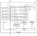
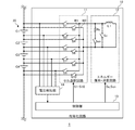
- FIG. 1 is a diagram illustrating a configuration of a power storage system according to an embodiment of the present invention.
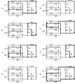
- FIGS. 2A to 2H are diagrams for explaining an operation sequence example of the equalization processing of the power storage system according to the embodiment of the present invention.
- FIGS. 3A to 3C are diagrams illustrating a specific example 1 of the equalization processing of the power storage system according to the embodiment of the present invention.
- FIGS. 4A and 4B are diagrams illustrating a specific example 2 of the equalization processing of the power storage system according to the embodiment of the present invention.
- FIGS. 5A and 5B are diagrams illustrating a specific example 3 of the equalization processing of the power storage system according to the embodiment of the present invention.
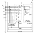
- FIG. 6 is a diagram illustrating a configuration of a power storage system according to a comparative example.
- FIG. 9 is a diagram illustrating a configuration of a power storage system according to Modification Example 1 of the present invention.
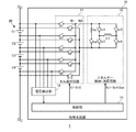
- FIG. 13 is a diagram illustrating a configuration of a power storage system according to Modification 2 of the present invention.
- FIG. 13 is a diagram illustrating a configuration of a power storage system according to Modification 3 of the present invention.
- FIG. 1 is a diagram showing a configuration of a power storage system 1 according to an embodiment of the present invention.
- the power storage system 1 includes an equalization circuit 10 and a power storage unit 20.
- Power storage unit 20 includes n (n is an integer of 2 or more) cells connected in series.
- FIG. 1 illustrates an example in which four cells C1 to C4 are connected in series. Note that the number of cells connected in series varies according to the voltage specifications required for power storage system 1.
- Each cell can be a chargeable / dischargeable power storage element such as a lithium ion battery cell, a nickel hydrogen battery cell, a lead battery cell, an electric double layer capacitor cell, and a lithium ion capacitor cell.
- a lithium ion battery cell nominal voltage: 3.6 to 3.7 V
- the equalization circuit 10 includes a voltage detection unit 14, a cell selection circuit 11, an energy holding / consuming circuit 12, and a control unit 13.
- the voltage detector 14 detects each voltage of n (4 in FIG. 1) cells connected in series. Specifically, the voltage detection unit 14 is connected to each node of n cells connected in series by (n + 1) voltage lines, and detects a voltage between two adjacent voltage lines, respectively. , And detect the voltage of each cell.
- the voltage detection unit 14 can be configured by, for example, a general-purpose analog front-end IC or an ASIC (Application Specific Integrated Circuit). The voltage detector 14 converts the detected voltage of each cell into a digital value and outputs the digital value to the controller 13.
- the cell selection circuit 11 is provided between the n cells connected in series and the inductor L1 included in the energy holding / consuming circuit 12, and includes both ends of a cell selected from the n cells and an inductor This is a circuit capable of conducting both ends of L1.
- the cell selection circuit 11 includes a first wiring W1 connected to the first end of the inductor L1, a second wiring W2 connected to the second end of the inductor L1, (n + 1) first wiring side switches, and (n + 1) ) Second wiring-side switches.
- the (n + 1) first wiring side switches are respectively connected between each node of the n cells connected in series and the first wiring W1.
- the (n + 1) second wiring side switches are respectively connected between the respective nodes of the n cells connected in series and the second wiring W2.
- the first switch S1, the third switch S3, the fifth switch S5, the seventh switch S7, and the ninth switch S9 are first wiring side switches
- the second switch S2, the fourth switch S4, and the sixth switch S6, the eighth switch S8, and the tenth switch S10 are second wiring side switches.
- the energy holding / consuming circuit 12 includes an inductor L1, a clamp switch Sc, a resistor Rc, and a bypass switch Sb.
- the clamp switch Sc is a switch for conducting both ends of the inductor L1 in the energy holding / consuming circuit 12.
- the resistance Rc is a resistance element for consuming energy.
- the bypass switch Sb is connected in parallel with the resistor Rc, and is a switch for forming a path for bypassing the resistor Rc.
- the energy holding and consuming circuit 12 can form a closed loop including the inductor L1 in a state where the cell selection circuit 11 has not selected any cells. Further, the energy holding / consuming circuit can form a closed loop of a first pattern having a small closed loop resistance component and a closed loop of a second pattern having a large closed loop resistance component.
- a closed loop of the first pattern including the inductor L1, the clamp switch Sc, and the bypass switch Sb is formed.
- a closed loop of a second pattern including the inductor L1, the clamp switch Sc, and the resistor Rc is formed.
- the closed loop of the first pattern is a closed loop for holding energy in the energy holding / consuming circuit 12.
- the closed loop of the second pattern is a closed loop for consuming energy in the energy holding / consuming circuit 12.
- MOSFETs Metal-Oxide-Semiconductor Field-Effect Transistors
- IGBTs Insulated Gate Bipolar Transistors
- the control unit 13 performs equalization processing among the n cells connected in series based on the voltages of the n cells detected by the voltage detection unit 14.
- the control unit 13 can be composed of, for example, a microcomputer. Note that the control unit 13 and the voltage detection unit 14 may be integrated into one chip.
- control unit 13 executes equalization processing between n cells connected in series by the active cell balance method.
- energy is transferred from one cell (cell to be discharged) to another cell (cell to be charged) between n cells connected in series. Equalize the capacity of one cell with another cell. By repeating this energy transfer, the capacity between the n cells connected in series is equalized.
- the control unit 13 controls the cell selection circuit 11 to make both ends of the cell to be discharged out of the n cells and both ends of the inductor L1 conductive for a predetermined time. In this state, a current flows from the discharge target cell to the inductor L1, and energy is accumulated in the inductor L1.
- control unit 13 controls the cell selection circuit 11 to electrically cut off the n cells and the inductor L1, and turns on the clamp switch Ss and the bypass switch Sb. In this state, a circulating current flows through the closed loop of the first pattern, and the inductor current is actively clamped in the energy holding / consuming circuit 12.
- control unit 13 turns off the clamp switch Sc and the bypass switch Sb, and controls the cell selection circuit 11 so that both ends of the cell to be charged and both ends of the inductor L1 among the n cells are set for a predetermined time. Make it conductive. In this state, the inductor current actively clamped in the energy holding / consuming circuit 12 flows to the cell to be charged. Thus, energy transfer from one cell to another cell is completed.
- FIGS. 2A to 2H are diagrams for explaining an operation sequence example of the equalization processing of the power storage system 1 according to the embodiment of the present invention.
- the number of series cells is set to 2 for simplification of the description.
- the control unit 13 controls the first switch S1 and the fourth switch S4 to be in the on state, and the second switch S2, the third switch S3, the fifth switch S5, and the sixth switch S5.
- the switch S6, the clamp switch Sc, and the bypass switch Sb are turned off.
- a current flows from the first cell C1 to the inductor L1, and energy discharged from the first cell C1 is stored in the inductor L1.
- the control unit 13 controls the clamp switch Sc and the bypass switch Sb to be in the ON state, and the first switch S1, the second switch S2, the third switch S3, and the fourth switch S4. , The fifth switch S5 and the sixth switch S6 are controlled to be turned off.
- the energy stored in the inductor L1 flows through the closed loop of the first pattern as the inductor current, and is actively clamped.
- the control unit 13 controls the fourth switch S4 and the fifth switch S5 to be in the on state, and controls the first switch S1, the second switch S2, the third switch S3, and the sixth switch S5.
- the switch S6, the clamp switch Sc, and the bypass switch Sb are turned off.
- the inductor current actively clamped in the closed loop of the first pattern flows through the second cell C2, and the second cell C2 is charged.
- the control unit 13 includes the first switch S1, the second switch S2, the third switch S3, the fourth switch S4, the fifth switch S5, the sixth switch S6, and the clamp switch Sc. And the bypass switch Sb is turned off.
- This state is a state where the energy transfer from the first cell C1 to the second cell C2 has been completed.
- the control unit 13 controls the third switch S3 and the sixth switch S6 to be in the ON state, and controls the first switch S1, the second switch S2, the fourth switch S4, and the fifth switch S4.
- the switch S5, the clamp switch Sc and the bypass switch Sb are turned off.
- a current flows from the second cell C2 to the inductor L1, and energy discharged from the first cell C1 is stored in the inductor L1.
- the control unit 13 controls the clamp switch Sc and the bypass switch Sb to be in the ON state, and the first switch S1, the second switch S2, the third switch S3, and the fourth switch S4. , The fifth switch S5 and the sixth switch S6 are controlled to be turned off.
- the energy stored in the inductor L1 flows through the closed loop of the first pattern as the inductor current, and is actively clamped.
- the control unit 13 controls the second switch S2 and the third switch S3 to be in the ON state, and the first switch S1, the fourth switch S4, the fifth switch S5, and the sixth switch S5.
- the switch S6, the clamp switch Sc, and the bypass switch Sb are turned off.
- the inductor current actively clamped in the closed loop of the first pattern flows through the first cell C1, and the first cell C1 is charged.
- the control unit 13 includes the first switch S1, the second switch S2, the third switch S3, the fourth switch S4, the fifth switch S5, the sixth switch S6, and the clamp switch Sc. And the bypass switch Sb is turned off. In this state, the energy transfer from the second cell C2 to the first cell C1 is completed.
- the inductor current is actively clamped in the closed loop of the first pattern, so that the continuity of the inductor current is ensured, so that the cell selection circuit 11 can switch safely and reliably.
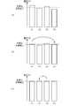
- FIGS. 3A to 3C are diagrams illustrating a specific example 1 of the equalization processing of the power storage system 1 according to the embodiment of the present invention.
- FIG. 3A is a diagram schematically showing the voltage states of the first cell C1 to the fourth cell C4 before the start of the equalization processing.
- the control unit 13 calculates an average value of the voltages of the first cell C1 to the fourth cell C4 detected by the voltage detection unit 14, and sets the calculated average value as an equalization target voltage (hereinafter, simply referred to as a target voltage). I do.
- the control unit 13 transfers energy from a cell higher than the target voltage to a cell lower than the target voltage. For example, among the cells having a voltage higher than the target voltage, the cell having the highest voltage (first cell C1 in FIG. 3A), and the cell having the lowest voltage among the cells having a voltage lower than the target voltage (first cell C1 in FIG. 3A). The energy is transferred to the four cells C4).
- the control unit 13 performs energy transfer in a range where the voltage of the source cell (cell to be discharged) is equal to or higher than the target voltage and in a range where the voltage of the destination cell (cell to be charged) is equal to or lower than the target voltage. Determine the amount.
- the control unit 13 determines the discharge time of the transfer source cell and the charge time of the transfer destination cell based on the determined energy transfer amount and the discharge current and the charge current based on the design. Since the amount of energy consumed while being actively clamped by the energy holding / consuming circuit 12 is negligible, the discharge time of the source cell and the charge time of the destination cell are basically the same.
- FIG. 3B shows a state in which the energy transfer from the first cell C1 as the source cell to the fourth cell C4 as the destination cell is completed.
- the control unit 13 executes the above-described processing again. Specifically, the cell having the highest voltage (third cell C3 in FIG. 3B) among the cells having a voltage higher than the target voltage, and the cell having the lowest voltage among the cells having a voltage lower than the target voltage (FIG. 3B) In (2), energy is transferred to the second cell C2).
- FIG. 3 (c) shows a state in which energy transfer from the third cell C3, which is the source cell, to the second cell C2, which is the destination cell, is completed.
- the equalization processing of the four cells C1-C4 connected in series is completed.
- an average value of voltages of a plurality of cells connected in series was calculated and a target value was set.
- an algorithm that does not set a target value is also possible.
- the control unit 13 equalizes the voltages of the two cells by transferring energy from the highest voltage cell to the lowest voltage cell among the voltages of the plurality of cells connected in series. The control unit 13 repeatedly executes this process until the voltages of the plurality of cells connected in series are all equalized.
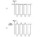
- FIGS. 4A and 4B are diagrams illustrating a specific example 2 of the equalization processing of the power storage system 1 according to the embodiment of the present invention.
- FIG. 4A shows the voltage of the highest voltage cell (first cell C1 in FIG. 4A) and the lowest voltage cell (first cell C1 to fourth cell C4) of the first cell C1 to fourth cell C4 connected in series.
- FIG. 4A shows a case where the amount of energy to be transferred between the cells based on the difference ⁇ V from the voltage of the fourth cell C4) is smaller than the set value.
- the minimum amount of energy that can be transferred from one cell to another is limited by the operating speed of the switch.
- the ON resistance of a MOSFET tends to increase as the operating speed increases. If a MOSFET with a low on-resistance is used to suppress the loss and heat generation due to the on-resistance, the operation speed is reduced. As the operation speed of the switch decreases, the minimum value of the amount of energy that can be passed by turning the switch on and off increases.
- the above set values are mainly values determined in advance by the designer based on the operation speed of the switch being used. That is, the set value is a value that defines the minimum control unit when transferring energy between cells.
- the control unit 13 controls the cell selection circuit 11 so that both ends of the cell to be discharged and both ends of the inductor L1 are electrically connected for a predetermined time. Let it. In this state, a current flows from the discharge target cell to the inductor L1, and energy is accumulated in the inductor L1.
- control unit 13 controls the cell selection circuit 11 to electrically cut off the n cells and the inductor L1, and turns on the clamp switch Ss. Note that the bypass switch Sb is not turned on. In this state, the circulating current flows through the closed loop of the second pattern, and the inductor current is consumed in the energy holding / consuming circuit 12.
- the control unit 13 determines which one of the first to fourth cells C4 connected in series has the lowest voltage.
- the voltage of the four cells C4 is set to a target value.
- the control unit 13 calculates the discharge time required for adjusting the voltage of the first cell C1 to the target value by consuming the capacity of the first cell C1 by the resistor Rc in the energy holding / consuming circuit 12.
- the control unit 13 controls the cell selection circuit 11 to make both ends of the first cell C1 and both ends of the inductor L1 conductive for the calculated discharge time.
- FIG. 4B shows a state in which the equalization processing of the first cell C1 to the fourth cell C4 connected in series is completed by the energy consumption of the first cell C1 to the third cell C3.
- FIGS. 5A and 5B are diagrams illustrating a specific example 3 of the equalization processing of the power storage system 1 according to the embodiment of the present invention.
- FIG. 5A shows that, among a plurality of cells connected in series, the amount of energy to be transferred between the cells based on the difference ⁇ V between the voltage of the cell with the highest voltage and the voltage of the cell with the lowest voltage. This shows a case where the voltages of a plurality of cells other than the cell having the highest voltage and smaller than the set value are uniform.
- FIG. 5A shows a state in which the equalization processing of the first cell C1 to the fourth cell C4 connected in series has been completed due to the energy consumption of the first cell C1.
- a predetermined value may be added to the set value to increase the set value.
- the processing time is greatly reduced by consuming the energy of one cell with a high voltage, rather than dividing the energy and sequentially transferring the divided energy to a plurality of other cells. I do. Therefore, a design that increases the number of cases where the energy of the cell is consumed when the voltage of only one cell is high is one of effective designs.
- FIG. 6 is a diagram illustrating a configuration of a power storage system 1 according to a comparative example.
- the configuration of the power storage system 1 according to the comparative example is different from the configuration of the power storage system 1 according to the embodiment illustrated in FIG. 1 in that the energy holding / consuming circuit 12 is replaced with an energy holding circuit 12a.
- the configuration of the energy holding circuit 12a is a configuration in which the resistor Rc and the bypass switch Sb are removed from the energy holding / consuming circuit 12.
- the energy holding circuit 12a is a circuit having no function of consuming the energy stored in the inductor L1 by the resistor Rc.
- a general passive-type circuit configuration is added. That is, a discharge circuit is provided in parallel with each cell. Specifically, a first discharge switch Sd1 and a first discharge resistor Rd1 are connected in series at both ends of the first cell E1, and a second discharge switch Sd2 and a second discharge resistor Rd2 are connected in series at both ends of the second cell E2. The third discharge switch Sd3 and the third discharge resistor Rd3 are connected in series to both ends of the third cell E3, and the fourth discharge switch Sd4 and the fourth discharge resistor Rd4 are connected in series to both ends of the fourth cell E4.
- the radiation space for the discharge resistor for the passive cell balance is secured for each cell on the substrate, and the active cell balance circuit is used. Installation space is required, and there is much waste in design.
- the discharge resistance for passive cell balancing can be one of the resistances Rc in the energy holding / consuming circuit 12. Therefore, the heat dissipation space of the discharge resistor can be reduced to 1 / n as compared with the configuration according to the comparative example. Also, the number of components (resistors and switches) required for passive cell balance can be reduced to 1 / n.
- a general active equalization circuit is capable of transferring energy while suppressing heat generation between a plurality of cells, and thus is suitable for large energy transfer. It may be difficult to fine-tune the capacitance between them.
- a general passive equalizing circuit cannot transfer energy between a plurality of cells, but can easily perform fine adjustment of the capacity between a plurality of cells.
- the equalizing circuit by providing the energy holding / consuming circuit 12, active cell balancing is realized by active clamping of the inductor current, and passive cell balancing is also achieved by consuming energy with the resistor Rc. Can be realized. Therefore, both large energy transfer between a plurality of cells and fine adjustment of the capacity between the plurality of cells are possible, and the advantages of both the active method and the passive method can be enjoyed.
- FIG. 7 is a diagram showing a configuration of a power storage system 1 according to a first modification of the present invention.
- a conduction switch Scn is used instead of the bypass switch Sb.
- the resistor Rc and the conduction switch Scn connected in series are connected in parallel with the clamp switch Sc.
- the number of switches through which the current passes in the closed loop of the first pattern is two in the basic example and one in the first modification.
- the number of switches through which current passes in the closed loop of the second pattern is 1 in both the basic example and the first modification. Therefore, the first modification can reduce the power loss when the inductor current is actively clamped.
- FIG. 8 is a diagram showing a configuration of a power storage system 1 according to a second modification of the present invention.
- the clamp switch in the energy holding / consuming circuit 12 has a full bridge configuration.
- the first clamp switch Sc1 and the second clamp switch Sc2 are connected in series between the first wiring W1 and the second wiring W2.
- a third clamp switch Sc3 and a fourth clamp switch Sc4 are connected in series between the first wiring W1 and the second wiring W2 in parallel with the first clamp switch Sc1 and the second clamp switch Sc2.
- a first end of the inductor L1 is connected to a midpoint between the first clamp switch Sc1 and the second clamp switch Sc2, and a second end of the inductor L1 is connected to a midpoint between the third clamp switch Sc3 and the fourth clamp switch Sc4. Is done. Further, a resistor Rc and a conduction switch Scn connected in series are connected between both ends of the inductor L1.
- the direction of the discharge current or the charge current can be arbitrarily selected.
- the first switch S1 to the tenth switch S10 are configured as bidirectional switches, the direction of the discharge current or the charge current can be arbitrarily selected.
- FIG. 9 is a diagram showing a configuration of a power storage system 1 according to Modification 3 of the present invention.
- the clamp switch in the energy holding / consuming circuit 12 has a full bridge configuration.
- the resistor Rc and the conduction switch Scn connected in series are connected between the first wiring W1 and the second wiring W2. Others are the same as the modification 2.
- the resistor Rc and the bypass switch Sb (conduction switch Scn) in the energy holding / consuming circuit 12 may be omitted.
- the resistor Rc is substituted by the equivalent series resistance of the inductor L1 and / or the on-resistance of the MOSFET.
- the effect of retaining energy increases as the maintenance time of the closed loop formed by turning on the clamp switch Sc decreases, and the effect of consuming energy increases as the maintenance time of the closed loop increases.
- This modification is also one of the effective options in applications where the equalization processing time can be allowed to be long.
- the embodiments may be specified by the following items.
- a cell selection circuit (11) capable of An energy holding and consuming circuit (12) for forming a closed loop including the inductor (L1) in a state where the cell selection circuit (11) has not selected any cell;
- the energy holding and consuming circuit (12) can form a closed loop of a first pattern having a small closed loop resistance component and a closed loop of a second pattern having a large closed loop resistance component (10). .
- fine adjustment of the capacitance between the plurality of cells (C1-C4) can be easily performed while suppressing an increase in circuit area.
- the control unit (13) calculates a target voltage / n of the n cells (C1-C4) based on the voltages of the n cells (C1-C4) detected by the voltage detection unit (14).
- a target capacity is determined, cells (C1-C4) higher than the target voltage / target capacity are determined as cells to be discharged, and cells lower than the target voltage / target capacity are determined as cells to be charged.
- the equalization circuit (10) according to item 1 or 2. According to this, active cell balance by energy transfer between cells (C1 to C4) can be realized.
- the cell selection circuit (11) includes: A first wiring (W1) connected to one end of the inductor (L1); A second wiring (W2) connected to the other end of the inductor (L1); (N + 1) first wiring side switches (S1, S3, S5, S7) connected between the nodes of the n cells (C1-C4) connected in series and the first wiring (W1), respectively. , S9), (N + 1) second wiring side switches (S2, S4, S6, S8) connected between each node of the n cells (C1-C4) connected in series and the second wiring (W2), respectively. , S10),
- the equalizing circuit (10) according to any one of items 1 to 4, wherein the equalizing circuit (10) includes: According to this, the active type equalizing circuit (10) can be realized with a small number of switches.
- N is an integer of 2 or more cells (C1-C4) connected in series;
- An equalizing circuit (10) according to any one of items 1 to 5,
- a power storage system (1) comprising: According to this, in the active equalization circuit (10), the power storage system (1) that can easily perform fine adjustment of the capacity between the plurality of cells (C1 to C4) while suppressing an increase in circuit area. Can be built.
- a module selection circuit (11) capable of An energy holding and consuming circuit (12) for forming a closed loop including the inductor (L1) when the module selection circuit (11) has not selected any module;
- the energy holding and consuming circuit (12) can form a closed loop of a first pattern having a small closed loop resistance component and a closed loop of a second pattern having a large closed loop resistance component (10). .
- fine adjustment of the capacitance between the plurality of modules (C1-C4) can be easily performed while suppressing an increase in circuit area.
- N is an integer of 2 or more modules (C1-C4) connected in series;
- An equalizing circuit (10) according to item 7,
- a power storage system (1) comprising: According to this, in the active equalizing circuit (10), the power storage system (1) that can easily perform fine adjustment of the capacity between the plurality of modules (C1 to C4) while suppressing an increase in circuit area. Can be built.
- 1 ⁇ energy storage system ⁇ 10 ⁇ equalization circuit, ⁇ 11 ⁇ cell selection circuit, ⁇ 12 ⁇ energy holding / consumption circuit, ⁇ 12a ⁇ energy holding circuit, ⁇ 13 ⁇ control section, ⁇ 14 ⁇ voltage detection section, ⁇ 20 ⁇ storage section, ⁇ C1-C4 ⁇ cell, ⁇ S1-S10 ⁇ switch, ⁇ W1 1st wiring, ⁇ W2 ⁇ 2nd wiring, ⁇ L1 ⁇ inductor, ⁇ Sc-Sc4 ⁇ clamp switch, ⁇ Sb ⁇ bypass switch, ⁇ Scn ⁇ conduction switch, ⁇ Rc ⁇ resistance.
Landscapes
- Engineering & Computer Science (AREA)
- Power Engineering (AREA)
- Manufacturing & Machinery (AREA)
- Chemical & Material Sciences (AREA)
- Chemical Kinetics & Catalysis (AREA)
- Electrochemistry (AREA)
- General Chemical & Material Sciences (AREA)
- Physics & Mathematics (AREA)
- General Physics & Mathematics (AREA)
- Charge And Discharge Circuits For Batteries Or The Like (AREA)
- Secondary Cells (AREA)
Abstract
L'invention concerne un circuit d'égalisation dans lequel un circuit de sélection d'élément est agencé entre n éléments et une bobine d'induction, et permet une conduction entre les deux extrémités de l'un des n éléments et les deux extrémités de la bobine d'induction. Un circuit de maintien d'énergie / consommation permet de former une boucle fermée incluant la bobine d'induction dans un état dans lequel le circuit de sélection d'élément ne sélectionne aucun des éléments. Le circuit de maintien d'énergie / consommation permet de former une boucle fermée d'un premier motif présentant un petit composant résistance de boucle fermée, et une boucle fermée d'un second motif présentant un grand composant résistance de boucle fermée.
Priority Applications (3)
| Application Number | Priority Date | Filing Date | Title |
|---|---|---|---|
| US17/266,173 US11437828B2 (en) | 2018-09-06 | 2019-08-01 | Equalization circuit and power storage system |
| CN201980054077.8A CN112567587B (zh) | 2018-09-06 | 2019-08-01 | 均等化电路以及蓄电系统 |
| JP2020541065A JP7320737B2 (ja) | 2018-09-06 | 2019-08-01 | 均等化回路、及び蓄電システム |
Applications Claiming Priority (2)
| Application Number | Priority Date | Filing Date | Title |
|---|---|---|---|
| JP2018-167046 | 2018-09-06 | ||
| JP2018167046 | 2018-09-06 |
Publications (1)
| Publication Number | Publication Date |
|---|---|
| WO2020049910A1 true WO2020049910A1 (fr) | 2020-03-12 |
Family
ID=69721868
Family Applications (1)
| Application Number | Title | Priority Date | Filing Date |
|---|---|---|---|
| PCT/JP2019/030198 Ceased WO2020049910A1 (fr) | 2018-09-06 | 2019-08-01 | Circuit d'égalisation, et système d'accumulation |
Country Status (4)
| Country | Link |
|---|---|
| US (1) | US11437828B2 (fr) |
| JP (1) | JP7320737B2 (fr) |
| CN (1) | CN112567587B (fr) |
| WO (1) | WO2020049910A1 (fr) |
Cited By (5)
| Publication number | Priority date | Publication date | Assignee | Title |
|---|---|---|---|---|
| JP2022546518A (ja) * | 2019-12-06 | 2022-11-04 | ジャン、チャオジョン | 並列および直列で電池を形成しかつテストするシステム |
| JP2023538390A (ja) * | 2021-02-24 | 2023-09-07 | エルジー・ケム・リミテッド | 引張強度に優れたポリ(乳酸-b-3-ヒドロキシプロピオン酸)ブロック共重合体およびそれを含む物品 |
| JP2023539228A (ja) * | 2021-02-24 | 2023-09-13 | エルジー・ケム・リミテッド | 透明性特性に優れたポリ(乳酸-b-3-ヒドロキシプロピオン酸)ブロック共重合体およびこれを含む物品 |
| EP4238805A4 (fr) * | 2020-11-02 | 2024-10-09 | Imasen Electric Industrial Co., Ltd. | Dispositif source d'alimentation de véhicule |
| US12617888B2 (en) | 2021-02-24 | 2026-05-05 | Lg Chem, Ltd. | Poly(lactic acid-b-3-hydroxypropionic acid) block copolymer having excellent transparency property and products containing the same |
Families Citing this family (7)
| Publication number | Priority date | Publication date | Assignee | Title |
|---|---|---|---|---|
| US11894702B2 (en) * | 2018-09-06 | 2024-02-06 | Panasonic Intellectual Property Management Co., Ltd. | Energy transfer circuit and power storage system |
| CN112956101B (zh) * | 2018-11-02 | 2024-08-13 | 松下知识产权经营株式会社 | 能量移动电路以及蓄电系统 |
| CN114072983A (zh) * | 2019-05-16 | 2022-02-18 | 特洛斯公司 | 用于双均衡电池和电池组性能管理的方法和系统 |
| US12278508B2 (en) * | 2019-06-17 | 2025-04-15 | Renesas Electronics America Inc. | Single inductor multiple output charger for multiple battery applications |
| CN116154888A (zh) * | 2022-09-28 | 2023-05-23 | 湖北亿纬动力有限公司 | 簇间环流抑制系统及方法 |
| CN118040825A (zh) * | 2024-01-18 | 2024-05-14 | 华为数字能源技术有限公司 | 一种能量均衡系统及储能系统 |
| US12308674B1 (en) * | 2024-01-19 | 2025-05-20 | Moment Energy Inc. | Active energy balancing for energy storage systems |
Citations (4)
| Publication number | Priority date | Publication date | Assignee | Title |
|---|---|---|---|---|
| JP2007294322A (ja) * | 2006-04-26 | 2007-11-08 | Matsushita Electric Ind Co Ltd | 蓄電装置、携帯機器及び電動車両 |
| JP2013013292A (ja) * | 2011-06-30 | 2013-01-17 | Hitachi Ltd | インダクタを介したエネルギ移送によるセルバランス回路 |
| JP2015181333A (ja) * | 2014-03-04 | 2015-10-15 | 株式会社リコー | 蓄電状態調整回路、蓄電状態調整装置、蓄電池パック及びスイッチ回路の制御方法 |
| JP2016111905A (ja) * | 2014-02-28 | 2016-06-20 | 株式会社リコー | スイッチ回路の制御方法、蓄電状態調整回路、蓄電状態調整装置及び蓄電池パック |
Family Cites Families (8)
| Publication number | Priority date | Publication date | Assignee | Title |
|---|---|---|---|---|
| JP3328656B2 (ja) | 1994-05-25 | 2002-09-30 | 株式会社岡村研究所 | 電池の充電制御装置及び方法 |
| JP6205247B2 (ja) * | 2013-11-18 | 2017-09-27 | Fdk株式会社 | バランス補正装置及び蓄電装置 |
| CN103647327A (zh) * | 2013-12-23 | 2014-03-19 | 中国科学院电工研究所 | 一种用于电池组的充放电自动均衡装置 |
| US10770893B2 (en) * | 2014-05-02 | 2020-09-08 | The Governing Council Of The University Of Toronto | Multi-port converter structure for DC/DC power conversion |
| KR102124186B1 (ko) * | 2015-10-01 | 2020-06-17 | 주식회사 엘지화학 | 배터리 스택 밸런싱 장치 |
| CN106712191B (zh) * | 2017-01-10 | 2023-06-20 | 华南理工大学 | 基于外部储能单元与lc准谐振的电池组均衡电路及方法 |
| CN107104482A (zh) * | 2017-05-15 | 2017-08-29 | 广东工业大学 | 一种电压主动均衡电路及蓄电系统 |
| US11146076B2 (en) * | 2018-07-09 | 2021-10-12 | GM Global Technology Operations LLC | Battery module with active cell balancing using energy storage element and two tiers of switches |
-
2019
- 2019-08-01 JP JP2020541065A patent/JP7320737B2/ja active Active
- 2019-08-01 US US17/266,173 patent/US11437828B2/en active Active
- 2019-08-01 CN CN201980054077.8A patent/CN112567587B/zh active Active
- 2019-08-01 WO PCT/JP2019/030198 patent/WO2020049910A1/fr not_active Ceased
Patent Citations (4)
| Publication number | Priority date | Publication date | Assignee | Title |
|---|---|---|---|---|
| JP2007294322A (ja) * | 2006-04-26 | 2007-11-08 | Matsushita Electric Ind Co Ltd | 蓄電装置、携帯機器及び電動車両 |
| JP2013013292A (ja) * | 2011-06-30 | 2013-01-17 | Hitachi Ltd | インダクタを介したエネルギ移送によるセルバランス回路 |
| JP2016111905A (ja) * | 2014-02-28 | 2016-06-20 | 株式会社リコー | スイッチ回路の制御方法、蓄電状態調整回路、蓄電状態調整装置及び蓄電池パック |
| JP2015181333A (ja) * | 2014-03-04 | 2015-10-15 | 株式会社リコー | 蓄電状態調整回路、蓄電状態調整装置、蓄電池パック及びスイッチ回路の制御方法 |
Cited By (8)
| Publication number | Priority date | Publication date | Assignee | Title |
|---|---|---|---|---|
| JP2022546518A (ja) * | 2019-12-06 | 2022-11-04 | ジャン、チャオジョン | 並列および直列で電池を形成しかつテストするシステム |
| JP7400083B2 (ja) | 2019-12-06 | 2023-12-18 | ジャン、チャオジョン | 並列および直列で電池を形成しかつテストするシステム |
| EP4238805A4 (fr) * | 2020-11-02 | 2024-10-09 | Imasen Electric Industrial Co., Ltd. | Dispositif source d'alimentation de véhicule |
| JP2023538390A (ja) * | 2021-02-24 | 2023-09-07 | エルジー・ケム・リミテッド | 引張強度に優れたポリ(乳酸-b-3-ヒドロキシプロピオン酸)ブロック共重合体およびそれを含む物品 |
| JP2023539228A (ja) * | 2021-02-24 | 2023-09-13 | エルジー・ケム・リミテッド | 透明性特性に優れたポリ(乳酸-b-3-ヒドロキシプロピオン酸)ブロック共重合体およびこれを含む物品 |
| JP7618341B2 (ja) | 2021-02-24 | 2025-01-21 | エルジー・ケム・リミテッド | 透明性特性に優れたポリ(乳酸-b-3-ヒドロキシプロピオン酸)ブロック共重合体およびこれを含む物品 |
| JP7618340B2 (ja) | 2021-02-24 | 2025-01-21 | エルジー・ケム・リミテッド | 引張強度に優れたポリ(乳酸-b-3-ヒドロキシプロピオン酸)ブロック共重合体およびそれを含む物品 |
| US12617888B2 (en) | 2021-02-24 | 2026-05-05 | Lg Chem, Ltd. | Poly(lactic acid-b-3-hydroxypropionic acid) block copolymer having excellent transparency property and products containing the same |
Also Published As
| Publication number | Publication date |
|---|---|
| JPWO2020049910A1 (ja) | 2021-08-26 |
| CN112567587A (zh) | 2021-03-26 |
| JP7320737B2 (ja) | 2023-08-04 |
| US20210305816A1 (en) | 2021-09-30 |
| US11437828B2 (en) | 2022-09-06 |
| CN112567587B (zh) | 2024-05-24 |
Similar Documents
| Publication | Publication Date | Title |
|---|---|---|
| JP7320737B2 (ja) | 均等化回路、及び蓄電システム | |
| JP6813614B2 (ja) | インテリジェント電池の直流充電 | |
| KR101922370B1 (ko) | 전지 밸런싱 및 충전 장치 및 방법 | |
| CN107078509B (zh) | 电流流动控制器 | |
| JP7127064B2 (ja) | 管理装置、及び電源システム | |
| US10862318B2 (en) | Bilevel equalizer for battery cell charge management | |
| JP4126167B2 (ja) | 直列接続の電池群の充放電回路 | |
| US11894702B2 (en) | Energy transfer circuit and power storage system | |
| US12088129B2 (en) | Energy transfer circuit and power storage system | |
| CN106489222B (zh) | 控制电路 | |
| CN113875068B (zh) | 能量移动电路以及蓄电系统 | |
| JP7418457B2 (ja) | エネルギ移動回路、及び蓄電システム | |
| Singh et al. | Multimode-multilevel bidirectional converter for target battery equalization in a tandem connected battery units |
Legal Events
| Date | Code | Title | Description |
|---|---|---|---|
| 121 | Ep: the epo has been informed by wipo that ep was designated in this application |
Ref document number: 19858351 Country of ref document: EP Kind code of ref document: A1 |
|
| ENP | Entry into the national phase |
Ref document number: 2020541065 Country of ref document: JP Kind code of ref document: A |
|
| NENP | Non-entry into the national phase |
Ref country code: DE |
|
| 122 | Ep: pct application non-entry in european phase |
Ref document number: 19858351 Country of ref document: EP Kind code of ref document: A1 |