WO2020050195A1 - Élément d'imagerie à semi-conducteur et dispositif électronique - Google Patents
Élément d'imagerie à semi-conducteur et dispositif électronique Download PDFInfo
- Publication number
- WO2020050195A1 WO2020050195A1 PCT/JP2019/034348 JP2019034348W WO2020050195A1 WO 2020050195 A1 WO2020050195 A1 WO 2020050195A1 JP 2019034348 W JP2019034348 W JP 2019034348W WO 2020050195 A1 WO2020050195 A1 WO 2020050195A1
- Authority
- WO
- WIPO (PCT)
- Prior art keywords
- photoelectric conversion
- solid
- state imaging
- conversion element
- imaging device
- Prior art date
- Legal status (The legal status is an assumption and is not a legal conclusion. Google has not performed a legal analysis and makes no representation as to the accuracy of the status listed.)
- Ceased
Links
Images





Classifications
-
- H—ELECTRICITY
- H10—SEMICONDUCTOR DEVICES; ELECTRIC SOLID-STATE DEVICES NOT OTHERWISE PROVIDED FOR
- H10F—INORGANIC SEMICONDUCTOR DEVICES SENSITIVE TO INFRARED RADIATION, LIGHT, ELECTROMAGNETIC RADIATION OF SHORTER WAVELENGTH OR CORPUSCULAR RADIATION
- H10F39/00—Integrated devices, or assemblies of multiple devices, comprising at least one element covered by group H10F30/00, e.g. radiation detectors comprising photodiode arrays
- H10F39/10—Integrated devices
- H10F39/12—Image sensors
- H10F39/199—Back-illuminated image sensors
-
- H—ELECTRICITY
- H04—ELECTRIC COMMUNICATION TECHNIQUE
- H04N—PICTORIAL COMMUNICATION, e.g. TELEVISION
- H04N25/00—Circuitry of solid-state image sensors [SSIS]; Control thereof
- H04N25/70—SSIS architectures; Circuits associated therewith
-
- H—ELECTRICITY
- H04—ELECTRIC COMMUNICATION TECHNIQUE
- H04N—PICTORIAL COMMUNICATION, e.g. TELEVISION
- H04N25/00—Circuitry of solid-state image sensors [SSIS]; Control thereof
- H04N25/70—SSIS architectures; Circuits associated therewith
- H04N25/76—Addressed sensors, e.g. MOS or CMOS sensors
- H04N25/77—Pixel circuitry, e.g. memories, A/D converters, pixel amplifiers, shared circuits or shared components
-
- H—ELECTRICITY
- H10—SEMICONDUCTOR DEVICES; ELECTRIC SOLID-STATE DEVICES NOT OTHERWISE PROVIDED FOR
- H10F—INORGANIC SEMICONDUCTOR DEVICES SENSITIVE TO INFRARED RADIATION, LIGHT, ELECTROMAGNETIC RADIATION OF SHORTER WAVELENGTH OR CORPUSCULAR RADIATION
- H10F39/00—Integrated devices, or assemblies of multiple devices, comprising at least one element covered by group H10F30/00, e.g. radiation detectors comprising photodiode arrays
- H10F39/10—Integrated devices
- H10F39/12—Image sensors
- H10F39/18—Complementary metal-oxide-semiconductor [CMOS] image sensors; Photodiode array image sensors
-
- H—ELECTRICITY
- H10—SEMICONDUCTOR DEVICES; ELECTRIC SOLID-STATE DEVICES NOT OTHERWISE PROVIDED FOR
- H10F—INORGANIC SEMICONDUCTOR DEVICES SENSITIVE TO INFRARED RADIATION, LIGHT, ELECTROMAGNETIC RADIATION OF SHORTER WAVELENGTH OR CORPUSCULAR RADIATION
- H10F39/00—Integrated devices, or assemblies of multiple devices, comprising at least one element covered by group H10F30/00, e.g. radiation detectors comprising photodiode arrays
- H10F39/80—Constructional details of image sensors
- H10F39/803—Pixels having integrated switching, control, storage or amplification elements
- H10F39/8033—Photosensitive area
-
- H—ELECTRICITY
- H10—SEMICONDUCTOR DEVICES; ELECTRIC SOLID-STATE DEVICES NOT OTHERWISE PROVIDED FOR
- H10F—INORGANIC SEMICONDUCTOR DEVICES SENSITIVE TO INFRARED RADIATION, LIGHT, ELECTROMAGNETIC RADIATION OF SHORTER WAVELENGTH OR CORPUSCULAR RADIATION
- H10F39/00—Integrated devices, or assemblies of multiple devices, comprising at least one element covered by group H10F30/00, e.g. radiation detectors comprising photodiode arrays
- H10F39/80—Constructional details of image sensors
- H10F39/803—Pixels having integrated switching, control, storage or amplification elements
- H10F39/8037—Pixels having integrated switching, control, storage or amplification elements the integrated elements comprising a transistor
-
- H—ELECTRICITY
- H10—SEMICONDUCTOR DEVICES; ELECTRIC SOLID-STATE DEVICES NOT OTHERWISE PROVIDED FOR
- H10F—INORGANIC SEMICONDUCTOR DEVICES SENSITIVE TO INFRARED RADIATION, LIGHT, ELECTROMAGNETIC RADIATION OF SHORTER WAVELENGTH OR CORPUSCULAR RADIATION
- H10F39/00—Integrated devices, or assemblies of multiple devices, comprising at least one element covered by group H10F30/00, e.g. radiation detectors comprising photodiode arrays
- H10F39/80—Constructional details of image sensors
- H10F39/807—Pixel isolation structures
-
- H—ELECTRICITY
- H10—SEMICONDUCTOR DEVICES; ELECTRIC SOLID-STATE DEVICES NOT OTHERWISE PROVIDED FOR
- H10F—INORGANIC SEMICONDUCTOR DEVICES SENSITIVE TO INFRARED RADIATION, LIGHT, ELECTROMAGNETIC RADIATION OF SHORTER WAVELENGTH OR CORPUSCULAR RADIATION
- H10F39/00—Integrated devices, or assemblies of multiple devices, comprising at least one element covered by group H10F30/00, e.g. radiation detectors comprising photodiode arrays
- H10F39/80—Constructional details of image sensors
- H10F39/811—Interconnections
-
- H—ELECTRICITY
- H10—SEMICONDUCTOR DEVICES; ELECTRIC SOLID-STATE DEVICES NOT OTHERWISE PROVIDED FOR
- H10F—INORGANIC SEMICONDUCTOR DEVICES SENSITIVE TO INFRARED RADIATION, LIGHT, ELECTROMAGNETIC RADIATION OF SHORTER WAVELENGTH OR CORPUSCULAR RADIATION
- H10F39/00—Integrated devices, or assemblies of multiple devices, comprising at least one element covered by group H10F30/00, e.g. radiation detectors comprising photodiode arrays
- H10F39/80—Constructional details of image sensors
- H10F39/812—Arrangements for transferring the charges in the image sensor perpendicular to the imaging plane, e.g. buried regions used to transfer generated charges to circuitry under the photosensitive region
-
- H—ELECTRICITY
- H10—SEMICONDUCTOR DEVICES; ELECTRIC SOLID-STATE DEVICES NOT OTHERWISE PROVIDED FOR
- H10F—INORGANIC SEMICONDUCTOR DEVICES SENSITIVE TO INFRARED RADIATION, LIGHT, ELECTROMAGNETIC RADIATION OF SHORTER WAVELENGTH OR CORPUSCULAR RADIATION
- H10F39/00—Integrated devices, or assemblies of multiple devices, comprising at least one element covered by group H10F30/00, e.g. radiation detectors comprising photodiode arrays
- H10F39/80—Constructional details of image sensors
- H10F39/813—Electronic components shared by multiple pixels, e.g. one amplifier shared by two pixels
-
- H—ELECTRICITY
- H10—SEMICONDUCTOR DEVICES; ELECTRIC SOLID-STATE DEVICES NOT OTHERWISE PROVIDED FOR
- H10F—INORGANIC SEMICONDUCTOR DEVICES SENSITIVE TO INFRARED RADIATION, LIGHT, ELECTROMAGNETIC RADIATION OF SHORTER WAVELENGTH OR CORPUSCULAR RADIATION
- H10F39/00—Integrated devices, or assemblies of multiple devices, comprising at least one element covered by group H10F30/00, e.g. radiation detectors comprising photodiode arrays
- H10F39/011—Manufacture or treatment of image sensors covered by group H10F39/12
- H10F39/014—Manufacture or treatment of image sensors covered by group H10F39/12 of CMOS image sensors
Definitions
- the present technology relates to a solid-state imaging device. More specifically, the present invention relates to a solid-state imaging device that photoelectrically converts light from a subject and an electronic device.
- a known solid-state image sensor has a function of detecting not only visible light but also ultraviolet light.
- a technique has been proposed in which an ultraviolet light sensitive element and a visible light sensitive element are formed on a semiconductor substrate having an SOI (Silicon On Insulator) structure to be integrated into one chip (for example, see Patent Document 1).
- SOI Silicon On Insulator
- both the visible light sensitive element and the ultraviolet light sensitive element are formed on the silicon substrate.
- this conventional technique has a problem in that resolution is reduced because each light detection area is separately allocated in a plane in order to detect each of ultraviolet light and visible light. Further, since the Bayer arrangement is impossible, there is a problem that the color interpolation processing becomes difficult in addition to the reduction in the resolution.
- the present technology has been created in view of such a situation, and has an object to improve the resolution of a solid-state imaging device that detects visible light and ultraviolet light.
- the present technology has been made to solve the above-described problem, and a first aspect of the present technology is to accumulate a first photoelectric conversion element and a charge photoelectrically converted by the first photoelectric conversion element.
- an electronic device comprising: a connection portion connected to the storage portion for transferring the electric charge stored in the second storage portion to the other surface of the substrate. This brings about an effect of individually performing photoelectric conversion on both surfaces of the substrate.
- the first photoelectric conversion element photoelectrically converts light in a visible light region
- the second photoelectric conversion element is an ultraviolet light.
- the light in the light region may be photoelectrically converted. This brings about an effect that the visible light and the ultraviolet light are photoelectrically converted in one pixel.
- the substrate is a silicon substrate
- the second photoelectric conversion element is formed in a region having a depth of up to 40 nanometers from the surface of one surface of the substrate. You may.
- the first photoelectric conversion element is formed in a surface region of the other surface of the substrate.
- connection portion may be a conductor penetrating the substrate. This brings about an effect that the electric charge accumulated in the second accumulation part is transferred to the other surface through the substrate.
- this conductor may be formed to include at least tungsten.
- a hafnium film may be further provided on the surface of the second storage section. This has the effect of preventing reflection and suppressing dark current.
- a potential barrier may be further provided between the first accumulation unit and the second accumulation unit. This brings about an effect of separating charges of light having different wavelengths.
- the first photoelectric conversion element photoelectrically converts light of a plurality of colors different from each other
- the first storage unit stores the photoelectrically converted charge in a penetrating direction of the substrate. May be stored for each color. This brings about an effect that the color filter for each color becomes unnecessary.
- the second photoelectric conversion element is divided into left and right to perform photoelectric conversion, respectively, and the second storage unit is provided with the left and right divided second photoelectric conversion elements.
- the charge may be divided and stored in accordance with each of them. This brings about an effect that the autofocus is performed by detecting the phase difference based on the charge of the second photoelectric conversion element divided into right and left.
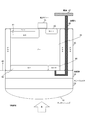
- FIG. 3 is a diagram illustrating a schematic example of a cross section of one pixel of the solid-state imaging device according to the first embodiment of the present technology.
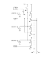
- FIG. 3 is a diagram illustrating an example of an equivalent circuit of one pixel of the solid-state imaging device according to the first embodiment of the present technology.
- FIG. 6 is a diagram illustrating an example of operation timing of the solid-state imaging device according to the first embodiment of the present technology.
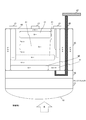
- FIG. 11 is a diagram illustrating a schematic example of a cross section of one pixel of a solid-state imaging device according to a second embodiment of the present technology.
- FIG. 13 is a diagram illustrating a schematic example of a cross section of one pixel of a solid-state imaging device according to a third embodiment of the present technology.
- FIG. 3 is a diagram illustrating a schematic example of a cross section of one pixel of the solid-state imaging device according to the first embodiment of the present technology.
- FIG. 3 is a diagram illustrating an example of an equivalent circuit
- FIG. 13 is a diagram illustrating a schematic example of a cross section of one pixel of a solid-state imaging device according to a fourth embodiment of the present technology.
- FIG. 15 is a diagram illustrating an example of an equivalent circuit of one pixel of a solid-state imaging device according to a fourth embodiment of the present technology.
- FIG. 21 is a diagram illustrating a schematic example of a cross section of one pixel of a solid-state imaging device according to a fifth embodiment of the present technology.
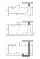
- FIG. 15 is a diagram illustrating an example of an equivalent circuit of one pixel of a solid-state imaging device according to a fifth embodiment of the present technology. It is the first half of the figure showing the example of the manufacturing process of the solid-state image sensing device in an embodiment of the present technology. It is the latter half of the figure showing the example of the manufacturing process of the solid-state image sensing device in an embodiment of the present technology.
- First embodiment (example in which an ultraviolet light detecting photodiode is provided on the back surface side) 2.
- Second embodiment an example in which a hafnium film is deposited on the back surface) 3.
- Third embodiment (example in which a potential barrier is provided immediately below a photodiode for detecting ultraviolet light) 4.
- Fourth embodiment (example in which a photodiode for visible light detection has a vertical spectral structure in silicon) 5.
- Fifth embodiment (example of detecting a phase difference using an ultraviolet light signal) 6.
- FIG. 1 is a diagram illustrating a schematic example of a cross section of one pixel of the solid-state imaging device according to the first embodiment of the present technology.
- a back-illuminated solid-state imaging device is assumed. That is, light from the subject enters from the back side (the lower side in the figure).
- an on-chip lens 10 a color filter 20, and an insulating film 30 are formed on a semiconductor substrate 40 from the back side.
- the color of the color filter 20 may be any color that transmits ultraviolet light and visible light. For example, it may be a clear (white) filter, or may be a green, red, blue, complementary color, or the like.
- the incident light incident from the back surface of the semiconductor substrate 40 through these is received by a photodiode (Photo Diode: PD) in the semiconductor substrate 40.
- the photodiode generates a charge according to incident light.
- the semiconductor substrate 40 has a photodiode 41 for photoelectrically converting visible light on the front side, and a photodiode 42 for photoelectrically converting ultraviolet light on the back side.
- the photodiodes 41 and 42 are loosely separated by a P-type well 49. In particular, photocharges having a wavelength of 400 nm (blue) or later move to the photodiode 41 due to this potential gradient.
- the photodiode 41 is an example of a first photoelectric conversion element described in the appended claims
- the photodiode 42 is an example of a second photoelectric conversion element described in the appended claims.
- the semiconductor substrate 40 is, for example, a P-type silicon substrate.
- the photodiode 41 includes an N + region formed on a P-type silicon substrate, and a P ++ region formed by diffusion or embedding in the N + region.
- the charge photoelectrically converted by the photodiode 41 is transferred to the storage unit 43 by the transfer gate 13 and stored.
- This accumulation section 43 is formed as an N ++ region.
- the storage unit 43 is an example of a first storage unit described in the claims.
- the photodiode 42 has an N- region formed on a P-type silicon substrate.
- the charge photoelectrically converted by the photodiode 42 is stored in the storage unit 44.
- This accumulation section 44 is formed as an N ++ region.
- the storage unit 44 is an example of a second storage unit described in the claims.
- the absorptivity of ultraviolet light having a wavelength of up to 400 nm with respect to silicon is approximately 100% in a region of silicon having a depth of 0 to 40 nm. Therefore, it is preferable that the photodiode 42 for ultraviolet light detection disposed on the rear surface side has a depletion region in a region from the rear surface side of the semiconductor substrate 40 to a depth of about 40 nm.
- the electric charge accumulated in the accumulation unit 44 is transferred to the wiring 47 on the front surface via the conductor 46.
- the conductor 46 is a conductive member that is connected to the storage unit 44 and penetrates the semiconductor substrate 40.
- the conductor 46 is formed at the center of the through electrode surrounded by the pinning region 45 (P ++) for preventing dark current.
- a metal material such as tungsten (W) can be adopted.
- the conductor 46 is an example of a connecting portion described in the claims.
- ultraviolet light can be detected by the photodiode 42 disposed on the back side of the semiconductor substrate 40 and visible light can be detected by the photodiode 41 disposed on the front side. Then, the photoelectrically converted charge is transferred to a circuit on the front surface side of the semiconductor substrate 40 via the transfer gate 13 and the conductor 46.
- FIG. 2 is a diagram illustrating an example of an equivalent circuit of one pixel of the solid-state imaging device according to the first embodiment of the present technology.
- This pixel includes a visible light photodiode 110, an ultraviolet light photodiode 120, a transfer transistor 130, a reset transistor 140, amplification transistors 151 and 152, and selection transistors 161 and 162.
- a transfer signal line TRX three signal lines of a transfer signal line TRX, a reset signal line RST, and a selection signal line SEL are provided in the row direction, and a visible light vertical signal line 191 and an ultraviolet light vertical signal are provided in the column direction.
- a line 192 is provided.
- the power supply voltage Vdd is supplied to the drain side of the reset transistor 140 and the amplification transistors 151 and 152.
- the visible light photodiode 110 corresponds to the above-described photodiode 41
- the ultraviolet light photodiode 120 corresponds to the above-described photodiode 42.
- the anodes of these photodiodes 110 and 120 are grounded.
- the transfer transistor 130 is a transistor that transfers the charge photoelectrically converted in the visible light photodiode 110.
- the transfer transistor 130 is provided between the cathode of the visible light photodiode 110 and the floating diffusion region FD (Floating @ Diffusion).
- the transfer transistor 130 is turned on when a high-level signal is input to the gate of the transfer transistor 130 from the vertical drive circuit via a transfer signal line, and transfers the charges photoelectrically converted by the visible light photodiode 110 to the floating diffusion region FD. Forward.
- the floating diffusion region FD is a diffusion layer region that converts the photoelectrically converted charge into a voltage signal.
- the voltage signal of floating diffusion region FD is connected to the drain of reset transistor 140 and the gates of amplification transistors 151 and 152.
- the floating diffusion region FD corresponds to the storage units 43 and 44 described above.
- the reset transistor 140 is a transistor for resetting the voltage of the floating diffusion region FD. This reset transistor 140 is provided between the power supply voltage Vdd and the floating diffusion region FD. The reset transistor 140 is turned on when a high-level signal is input to the reset signal line from the vertical drive circuit to the gate, and resets the potential of the floating diffusion region FD to the power supply voltage Vdd.
- the amplification transistors 151 and 152 are transistors that amplify the voltage signal of the floating diffusion region FD.
- the amplification transistors 151 and 152 amplify the voltage signal of the floating diffusion region FD, and output the amplified signal to the selection transistors 161 and 162 as a pixel signal, respectively.
- the selection transistors 161 and 162 are transistors for selecting this pixel.
- the selection transistors 161 and 162 are provided between the amplification transistors 151 and 152 and the vertical signal lines 191 and 192.
- the selection transistors 161 and 162 are turned on when a high-level signal is input to the selection signal line from the vertical drive circuit to the gates thereof, and the voltage signals amplified by the amplification transistors 151 and 152 are converted to the corresponding vertical signal. Output to lines 191 and 192.
- FIG. 3 is a diagram illustrating an example of operation timing of the solid-state imaging device according to the first embodiment of the present technology.
- the reset signal line RST and the transfer signal line TRX are asserted, whereby the charges of the visible light photodiode 110 and the ultraviolet light photodiode 120 are reset.
- the charges photoelectrically converted during the exposure are accumulated in the visible light photodiode 110 and the ultraviolet light photodiode 120, respectively.
- the visible light photodiode 110 accumulates light in the visible light region according to the silicon absorption rate
- the ultraviolet light photodiode 120 accumulates light in the ultraviolet light region.
- the selection signal line SEL is asserted, and the pixel is selected.
- the charge of the ultraviolet light initially stored in the ultraviolet light photodiode 120 is supplied to the amplification transistor 152, and the ultraviolet light signal is output to the vertical signal line 192.
- the reset signal line RST is asserted, thereby resetting the visible light and the ultraviolet light, and subsequently, the visible light photodiode 110 detects the visible light.
- the transfer signal line TRX is asserted, visible light charges are supplied to the amplification transistor 151, and a visible light signal is output to the vertical signal line 191.
- the ultraviolet light is detected by the photodiode 42 disposed on the back surface side of the semiconductor substrate 40, and the photodiode disposed on the front surface side is detected. With 41, visible light can be detected. The electric charge of the ultraviolet light photoelectrically converted by the photodiode 42 disposed on the rear surface side is efficiently transferred to the circuit on the front surface side of the semiconductor substrate 40 via the conductor 46.
- one pixel can detect both lights. Thereby, signals from ultraviolet light to visible light can be detected without lowering the resolution.
- the visible light signal detection employs an HAD (Hole-Accumulation Diode) structure in which the surface is covered with a P-type and has an embedded structure, and a transfer-type structure.
- HAD Hole-Accumulation Diode
- the ultraviolet light signal considering the main application of the ultraviolet light signal, a high SN ratio is not necessarily required, so that it is not necessary to use the HAD structure and the transfer type. Furthermore, if the silicon surface has an HAD structure, the charges generated on the outermost surface may diffuse to other nodes and may not be able to contribute as signal charges. On the other hand, in this embodiment, the HAD structure is not adopted for the ultraviolet light, and the accumulating portion is provided from the outermost surface. Therefore, it is possible to detect the ultraviolet light signal without losing the signal charge. .
- VFG Vertical Transfer Gate
- FIG. 4 is a diagram illustrating a schematic example of a cross section of one pixel of a solid-state imaging device according to the second embodiment of the present technology.
- a photodiode 41 for detecting visible light is disposed on the front surface side of the semiconductor substrate 40 and an ultraviolet light is disposed on the back surface side, similarly to the first embodiment.
- a photodiode 42 for detecting light is provided.
- a hafnium film 35 is deposited on the back surface of the semiconductor substrate 40.
- the hafnium film 35 is negatively charged and suppresses surface defects. Thereby, reflection can be prevented and dark current can be suppressed.
- the structure other than the hafnium film 35 is the same as that of the first embodiment. Also, the equivalent circuit is the same as in the first embodiment.
- the hafnium film 35 on the surface on the back side of the semiconductor substrate 40, it is possible to prevent reflection on the back side and suppress dark current. it can.
- FIG. 5 is a diagram illustrating a schematic example of a cross section of one pixel of a solid-state imaging device according to a third embodiment of the present technology.
- a photodiode 41 for detecting visible light is disposed on the front side of the semiconductor substrate 40, and an ultraviolet ray is disposed on the back side, as in the first embodiment.
- a photodiode 42 for detecting light is provided.
- a high-concentration P-type layer 48 is provided directly below the photodiode 42. This high-concentration P-type layer 48 functions as a potential barrier (potential barrier) for preventing the depletion layer from spreading. This makes it possible to easily separate the charges of the ultraviolet light and the blue light.
- the structure other than the high-concentration P-type layer 48 is the same as that of the above-described first embodiment. Also, the equivalent circuit is the same as in the first embodiment.
- the high-concentration P-type layer 48 serving as a potential barrier directly below the photodiode 42 charges of ultraviolet light and blue light are easily separated. be able to.
- FIG. 6 is a diagram illustrating a schematic example of a cross section of one pixel of a solid-state imaging device according to a fourth embodiment of the present technology.
- the solid-state imaging device is provided with a photodiode 42 for detecting ultraviolet light on the rear surface side, similarly to the above-described first embodiment.
- the photodiode 41 for detecting visible light is divided into three for each color. That is, the semiconductor device 40 has a longitudinal spectral structure in silicon in which red, green, and blue photodiodes 41 are arranged coaxially in the depth direction in order from the front surface side of the semiconductor substrate 40.
- a vertical transfer transistor is used to transfer the signal charges of each color.
- the white filter 21 is used to capture all colors. This makes it possible to further improve the ultraviolet light detection rate without regard to the effect of the ultraviolet light transmittance due to the arrangement of the color filters for each color.
- FIG. 7 is a diagram illustrating an example of an equivalent circuit of one pixel of the solid-state imaging device according to the fourth embodiment of the present technology.
- the solid-state imaging device includes photodiodes 111 to 113 and transfer transistors 131 to 133 for each color, different from the first embodiment.
- the photodiode 41 for detecting visible light is divided for each color, so that the ultraviolet light transmittance can be reduced by disposing the color filters for each color.
- the ultraviolet light detection rate can be further improved without considering the influence.
- FIG. 8 is a diagram illustrating a schematic example of a cross section of one pixel of a solid-state imaging device according to a fifth embodiment of the present technology.
- a photodiode 42 for detecting ultraviolet light is divided into two right and left parts, and a phase difference for autofocus phase difference detection is provided. Configure the pixel.
- the conventional phase difference detection pixel divides the visible light region into two, which causes a decrease in the sensitivity of visible light.
- the SN ratio of a visible light signal is most important in imaging or sensing applications.
- the ultraviolet light signal is used for the phase difference detection, it is possible to prevent a decrease in the sensitivity of the visible light signal.
- a conductor 46 is connected to each of the storage sections 44 of the photodiode 42 divided into right and left, and the electric charge stored in the storage section 44 is transferred to the wiring 47 on the front surface via the conductor 46. .
- FIG. 9 is a diagram illustrating an example of an equivalent circuit of one pixel of a solid-state imaging device according to a fifth embodiment of the present technology.
- a photodiode that detects ultraviolet light is divided into two photodiodes 121 and 122 in accordance with a phase difference between right and left. .
- Outputs of the photodiodes 121 and 122 are connected to gates of the amplification transistors 158 and 159.
- the pixel signals amplified by the amplification transistors 158 and 159 are output to the selection transistors 168 and 169, respectively.
- the selection signal line SEL1 is shared by the selection transistors 161 and 168, and one of the ultraviolet light signals and the visible light signal are commonly controlled.
- the selection signal line SEL2 is connected to the selection transistor 169, and the other of the ultraviolet light signals is controlled independently of one of the ultraviolet light signals.
- Manufacturing method> 10 and 11 are diagrams illustrating an example of a manufacturing process of the solid-state imaging device according to the embodiment of the present technology.
- a photodiode 42 for detecting ultraviolet light and a storage section 44 thereof are formed on the back surface side of the semiconductor substrate 40 as shown in FIG. Further, a pinning region 45 penetrating the semiconductor substrate 40 is formed.
- a photodiode 41 for detecting visible light and a storage part 43 thereof are formed on the back side of the semiconductor substrate 40. Then, the transfer gate 13 that transfers the electric charge from the photodiode 41 to the storage unit 43 is formed.
- a conductor 46 is formed on the front side of the semiconductor substrate 40 and connected to the wiring 47. Further, a through hole 38 is formed at the position of the conductor 46 from the back surface side of the semiconductor substrate 40 by dry etching or the like.
- a fixed charge film 39 is formed on the back surface side of the semiconductor substrate 40 including the through hole 38.
- the insulating film 30 is stacked on the fixed charge film 39 to fill the through hole 38.
- a through-hole is formed in the central portion of the insulating film 30 filled in the through-hole 38 until reaching the conductor 46 on the front side, and the conductor 46 is formed in this through-hole. Embed. Then, the conductor 46 is connected to the storage unit 44.
- the storage section 44 on the back side and the wiring 47 on the front side are connected via the conductor 46. Thereby, the electric charge of the ultraviolet light accumulated in the accumulation section 44 on the back side is transferred to the circuit on the front side and output as an ultraviolet light signal.
- the solid-state imaging device has been described in detail. However, this embodiment may be applied to an electronic device equipped with the solid-state imaging device.
- the processing procedure described in the above-described embodiment may be regarded as a method having these series of procedures, or a program for causing a computer to execute these series of procedures or a recording medium storing the program. May be caught.
- a recording medium for example, a CD (Compact Disc), an MD (MiniDisc), a DVD (Digital Versatile Disc), a memory card, a Blu-ray Disc (Blu-ray (registered trademark) Disc), or the like can be used.
- the present technology may have the following configurations.
- the substrate is a silicon substrate
- the first photoelectric conversion element is formed in a surface region of the other surface of the substrate.
- the connection unit is a conductor penetrating the substrate.
- the solid-state imaging device according to any one of (1) to (7), further including a potential barrier between the first storage unit and the second storage unit.
- the first photoelectric conversion element photoelectrically converts light of a plurality of colors different from each other;
- the solid-state imaging device according to any one of (1) to (8), wherein the first accumulation unit accumulates the photoelectrically converted charges for each color in a penetrating direction of the substrate.
- the second photoelectric conversion element is divided into left and right and performs photoelectric conversion respectively,
- the solid-state imaging device according to any one of (1) to (9), wherein the second storage unit is configured to store charge by being divided corresponding to each of the left and right second photoelectric conversion elements. element.
- the solid-state imaging device A first photoelectric conversion element; A first accumulation unit that accumulates charges photoelectrically converted by the first photoelectric conversion element; A second photoelectric conversion element; A second storage unit that is disposed on one surface of the substrate and stores the charge photoelectrically converted by the second photoelectric conversion element; A connection unit connected to the second storage unit and transferring the charge stored in the second storage unit to the other surface of the substrate.
Landscapes
- Engineering & Computer Science (AREA)
- Multimedia (AREA)
- Signal Processing (AREA)
- Solid State Image Pick-Up Elements (AREA)
- Transforming Light Signals Into Electric Signals (AREA)
Abstract
La présente invention améliore la résolution d'un élément d'imagerie à semi-conducteur qui détecte la lumière visible et la lumière ultraviolette à l'intérieur d'un pixel. Selon la présente invention, des premier et second éléments de conversion photoélectrique effectuent une conversion photoélectrique de lumière incidente, respectivement. Une première partie de stockage stocke une charge électrique qui est convertie de manière photoélectrique par le premier élément de conversion photoélectrique. La seconde partie de stockage est agencée sur une surface d'un substrat, et stocke une charge électrique qui est convertie de manière photoélectrique par le second élément de conversion photoélectrique. Une partie de connexion est connectée à la seconde partie de stockage de façon à transférer la charge électrique stockée dans la seconde partie de stockage à l'autre surface du substrat.
Priority Applications (1)
| Application Number | Priority Date | Filing Date | Title |
|---|---|---|---|
| US17/250,708 US11855108B2 (en) | 2018-09-04 | 2019-09-02 | Solid-state imaging element and electronic device |
Applications Claiming Priority (2)
| Application Number | Priority Date | Filing Date | Title |
|---|---|---|---|
| JP2018165458A JP2020038910A (ja) | 2018-09-04 | 2018-09-04 | 固体撮像素子および電子装置 |
| JP2018-165458 | 2018-09-04 |
Publications (1)
| Publication Number | Publication Date |
|---|---|
| WO2020050195A1 true WO2020050195A1 (fr) | 2020-03-12 |
Family
ID=69721643
Family Applications (1)
| Application Number | Title | Priority Date | Filing Date |
|---|---|---|---|
| PCT/JP2019/034348 Ceased WO2020050195A1 (fr) | 2018-09-04 | 2019-09-02 | Élément d'imagerie à semi-conducteur et dispositif électronique |
Country Status (3)
| Country | Link |
|---|---|
| US (1) | US11855108B2 (fr) |
| JP (1) | JP2020038910A (fr) |
| WO (1) | WO2020050195A1 (fr) |
Cited By (1)
| Publication number | Priority date | Publication date | Assignee | Title |
|---|---|---|---|---|
| WO2026074912A1 (fr) * | 2024-10-01 | 2026-04-09 | ソニーセミコンダクタソリューションズ株式会社 | Dispositif de détection de lumière et équipement électronique |
Families Citing this family (1)
| Publication number | Priority date | Publication date | Assignee | Title |
|---|---|---|---|---|
| JP2023174229A (ja) * | 2022-05-27 | 2023-12-07 | キヤノン株式会社 | 光電変換装置 |
Citations (5)
| Publication number | Priority date | Publication date | Assignee | Title |
|---|---|---|---|---|
| JP2009135314A (ja) * | 2007-11-30 | 2009-06-18 | Oki Semiconductor Co Ltd | フォトダイオードの製造方法およびそれを用いて形成されたフォトダイオード |
| JP2015038931A (ja) * | 2013-08-19 | 2015-02-26 | ソニー株式会社 | 固体撮像素子および電子機器 |
| WO2015151651A1 (fr) * | 2014-04-04 | 2015-10-08 | シャープ株式会社 | Photodétecteur et dispositif électronique mobile |
| WO2016147837A1 (fr) * | 2015-03-13 | 2016-09-22 | ソニー株式会社 | Élément d'imagerie à semi-conducteurs, procédé de commande et dispositif électronique |
| WO2017138197A1 (fr) * | 2016-02-09 | 2017-08-17 | ソニー株式会社 | Dispositif à semi-conducteur, procédé de fabrication d'un dispositif à semi-conducteur, élément de capture d'image à semi-conducteur, et appareil électronique |
Family Cites Families (2)
| Publication number | Priority date | Publication date | Assignee | Title |
|---|---|---|---|---|
| JP2009170615A (ja) | 2008-01-15 | 2009-07-30 | Oki Semiconductor Co Ltd | 光センサおよびそれを備えたフォトic |
| US10805567B2 (en) * | 2018-09-13 | 2020-10-13 | Semiconductor Components Industries, Llc | Imaging pixels with non-destructive readout capabilities |
-
2018
- 2018-09-04 JP JP2018165458A patent/JP2020038910A/ja active Pending
-
2019
- 2019-09-02 WO PCT/JP2019/034348 patent/WO2020050195A1/fr not_active Ceased
- 2019-09-02 US US17/250,708 patent/US11855108B2/en active Active
Patent Citations (5)
| Publication number | Priority date | Publication date | Assignee | Title |
|---|---|---|---|---|
| JP2009135314A (ja) * | 2007-11-30 | 2009-06-18 | Oki Semiconductor Co Ltd | フォトダイオードの製造方法およびそれを用いて形成されたフォトダイオード |
| JP2015038931A (ja) * | 2013-08-19 | 2015-02-26 | ソニー株式会社 | 固体撮像素子および電子機器 |
| WO2015151651A1 (fr) * | 2014-04-04 | 2015-10-08 | シャープ株式会社 | Photodétecteur et dispositif électronique mobile |
| WO2016147837A1 (fr) * | 2015-03-13 | 2016-09-22 | ソニー株式会社 | Élément d'imagerie à semi-conducteurs, procédé de commande et dispositif électronique |
| WO2017138197A1 (fr) * | 2016-02-09 | 2017-08-17 | ソニー株式会社 | Dispositif à semi-conducteur, procédé de fabrication d'un dispositif à semi-conducteur, élément de capture d'image à semi-conducteur, et appareil électronique |
Cited By (1)
| Publication number | Priority date | Publication date | Assignee | Title |
|---|---|---|---|---|
| WO2026074912A1 (fr) * | 2024-10-01 | 2026-04-09 | ソニーセミコンダクタソリューションズ株式会社 | Dispositif de détection de lumière et équipement électronique |
Also Published As
| Publication number | Publication date |
|---|---|
| US20210202545A1 (en) | 2021-07-01 |
| US11855108B2 (en) | 2023-12-26 |
| JP2020038910A (ja) | 2020-03-12 |
Similar Documents
| Publication | Publication Date | Title |
|---|---|---|
| JP6190392B2 (ja) | 固体撮像素子および電子機器 | |
| CN108111787B (zh) | 摄像器件 | |
| TWI742573B (zh) | 固體攝像元件及其製造方法以及電子機器 | |
| CN106449677B (zh) | 具有混合型异质结构的图像传感器 | |
| EP2980852B1 (fr) | Élément de détection d'image à semi-conducteur et système d'imagerie | |
| US8101978B2 (en) | Circuit and photo sensor overlap for backside illumination image sensor | |
| US9490282B2 (en) | Photosensitive capacitor pixel for image sensor | |
| JP5269425B2 (ja) | 固体撮像素子および固体撮像装置 | |
| CN102082155B (zh) | 固体摄像器件、相机、半导体器件及其制造方法 | |
| JP2012033583A (ja) | 固体撮像素子及びその製造方法、並びに撮像装置 | |
| JP2008543061A (ja) | グローバルシャッターを有するピン光ダイオード画素 | |
| JP2008294175A (ja) | 固体撮像装置およびカメラ | |
| US20150295007A1 (en) | Image sensor with dielectric charge trapping device | |
| TWI709235B (zh) | 固體攝像元件、其製造方法及電子機器 | |
| WO2018105334A1 (fr) | Élément de capture d'image à semi-conducteur et appareil électronique | |
| JP5167693B2 (ja) | 固体撮像装置およびカメラ | |
| US11855108B2 (en) | Solid-state imaging element and electronic device | |
| HK1212818B (en) | Image sensor pixel and image sensor |
Legal Events
| Date | Code | Title | Description |
|---|---|---|---|
| 121 | Ep: the epo has been informed by wipo that ep was designated in this application |
Ref document number: 19858263 Country of ref document: EP Kind code of ref document: A1 |
|
| NENP | Non-entry into the national phase |
Ref country code: DE |
|
| 122 | Ep: pct application non-entry in european phase |
Ref document number: 19858263 Country of ref document: EP Kind code of ref document: A1 |