WO2020054581A1 - Composant électronique et procédé de fabrication de composant électronique - Google Patents
Composant électronique et procédé de fabrication de composant électronique Download PDFInfo
- Publication number
- WO2020054581A1 WO2020054581A1 PCT/JP2019/035039 JP2019035039W WO2020054581A1 WO 2020054581 A1 WO2020054581 A1 WO 2020054581A1 JP 2019035039 W JP2019035039 W JP 2019035039W WO 2020054581 A1 WO2020054581 A1 WO 2020054581A1
- Authority
- WO
- WIPO (PCT)
- Prior art keywords
- copper
- particles
- solder
- metal
- electronic component
- Prior art date
- Legal status (The legal status is an assumption and is not a legal conclusion. Google has not performed a legal analysis and makes no representation as to the accuracy of the status listed.)
- Ceased
Links
Images







Classifications
-
- B—PERFORMING OPERATIONS; TRANSPORTING
- B22—CASTING; POWDER METALLURGY
- B22F—WORKING METALLIC POWDER; MANUFACTURE OF ARTICLES FROM METALLIC POWDER; MAKING METALLIC POWDER; APPARATUS OR DEVICES SPECIALLY ADAPTED FOR METALLIC POWDER
- B22F7/00—Manufacture of composite layers, workpieces, or articles, comprising metallic powder, by sintering the powder, with or without compacting wherein at least one part is obtained by sintering or compression
- B22F7/06—Manufacture of composite layers, workpieces, or articles, comprising metallic powder, by sintering the powder, with or without compacting wherein at least one part is obtained by sintering or compression of composite workpieces or articles from parts, e.g. to form tipped tools
- B22F7/08—Manufacture of composite layers, workpieces, or articles, comprising metallic powder, by sintering the powder, with or without compacting wherein at least one part is obtained by sintering or compression of composite workpieces or articles from parts, e.g. to form tipped tools with one or more parts not made from powder
-
- B—PERFORMING OPERATIONS; TRANSPORTING
- B22—CASTING; POWDER METALLURGY
- B22F—WORKING METALLIC POWDER; MANUFACTURE OF ARTICLES FROM METALLIC POWDER; MAKING METALLIC POWDER; APPARATUS OR DEVICES SPECIALLY ADAPTED FOR METALLIC POWDER
- B22F1/00—Metallic powder; Treatment of metallic powder, e.g. to facilitate working or to improve properties
- B22F1/05—Metallic powder characterised by the size or surface area of the particles
- B22F1/052—Metallic powder characterised by the size or surface area of the particles characterised by a mixture of particles of different sizes or by the particle size distribution
-
- B—PERFORMING OPERATIONS; TRANSPORTING
- B22—CASTING; POWDER METALLURGY
- B22F—WORKING METALLIC POWDER; MANUFACTURE OF ARTICLES FROM METALLIC POWDER; MAKING METALLIC POWDER; APPARATUS OR DEVICES SPECIALLY ADAPTED FOR METALLIC POWDER
- B22F3/00—Manufacture of workpieces or articles from metallic powder characterised by the manner of compacting or sintering; Apparatus specially adapted therefor ; Presses and furnaces
- B22F3/10—Sintering only
- B22F3/11—Making porous workpieces or articles
-
- B—PERFORMING OPERATIONS; TRANSPORTING
- B22—CASTING; POWDER METALLURGY
- B22F—WORKING METALLIC POWDER; MANUFACTURE OF ARTICLES FROM METALLIC POWDER; MAKING METALLIC POWDER; APPARATUS OR DEVICES SPECIALLY ADAPTED FOR METALLIC POWDER
- B22F5/00—Manufacture of workpieces or articles from metallic powder characterised by the special shape of the product
- B22F5/12—Manufacture of workpieces or articles from metallic powder characterised by the special shape of the product of wires
-
- B—PERFORMING OPERATIONS; TRANSPORTING
- B23—MACHINE TOOLS; METAL-WORKING NOT OTHERWISE PROVIDED FOR
- B23K—SOLDERING OR UNSOLDERING; WELDING; CLADDING OR PLATING BY SOLDERING OR WELDING; CUTTING BY APPLYING HEAT LOCALLY, e.g. FLAME CUTTING; WORKING BY LASER BEAM
- B23K35/00—Rods, electrodes, materials, or media, for use in soldering, welding, or cutting
- B23K35/02—Rods, electrodes, materials, or media, for use in soldering, welding, or cutting characterised by mechanical features, e.g. shape
- B23K35/0222—Rods, electrodes, materials, or media, for use in soldering, welding, or cutting characterised by mechanical features, e.g. shape for use in soldering or brazing
- B23K35/0244—Powders, particles or spheres; Preforms made therefrom
- B23K35/025—Pastes, creams or slurries
-
- B—PERFORMING OPERATIONS; TRANSPORTING
- B23—MACHINE TOOLS; METAL-WORKING NOT OTHERWISE PROVIDED FOR
- B23K—SOLDERING OR UNSOLDERING; WELDING; CLADDING OR PLATING BY SOLDERING OR WELDING; CUTTING BY APPLYING HEAT LOCALLY, e.g. FLAME CUTTING; WORKING BY LASER BEAM
- B23K35/00—Rods, electrodes, materials, or media, for use in soldering, welding, or cutting
- B23K35/22—Rods, electrodes, materials, or media, for use in soldering, welding, or cutting characterised by the composition or nature of the material
- B23K35/24—Selection of soldering or welding materials proper
- B23K35/26—Selection of soldering or welding materials proper with the principal constituent melting at less than 400°C
- B23K35/262—Sn as the principal constituent
-
- B—PERFORMING OPERATIONS; TRANSPORTING
- B23—MACHINE TOOLS; METAL-WORKING NOT OTHERWISE PROVIDED FOR
- B23K—SOLDERING OR UNSOLDERING; WELDING; CLADDING OR PLATING BY SOLDERING OR WELDING; CUTTING BY APPLYING HEAT LOCALLY, e.g. FLAME CUTTING; WORKING BY LASER BEAM
- B23K35/00—Rods, electrodes, materials, or media, for use in soldering, welding, or cutting
- B23K35/22—Rods, electrodes, materials, or media, for use in soldering, welding, or cutting characterised by the composition or nature of the material
- B23K35/24—Selection of soldering or welding materials proper
- B23K35/26—Selection of soldering or welding materials proper with the principal constituent melting at less than 400°C
- B23K35/264—Bi as the principal constituent
-
- C—CHEMISTRY; METALLURGY
- C22—METALLURGY; FERROUS OR NON-FERROUS ALLOYS; TREATMENT OF ALLOYS OR NON-FERROUS METALS
- C22C—ALLOYS
- C22C12/00—Alloys based on antimony or bismuth
-
- C—CHEMISTRY; METALLURGY
- C22—METALLURGY; FERROUS OR NON-FERROUS ALLOYS; TREATMENT OF ALLOYS OR NON-FERROUS METALS
- C22C—ALLOYS
- C22C13/00—Alloys based on tin
-
- H—ELECTRICITY
- H05—ELECTRIC TECHNIQUES NOT OTHERWISE PROVIDED FOR
- H05K—PRINTED CIRCUITS; CASINGS OR CONSTRUCTIONAL DETAILS OF ELECTRIC APPARATUS; MANUFACTURE OF ASSEMBLAGES OF ELECTRICAL COMPONENTS
- H05K1/00—Printed circuits
- H05K1/18—Printed circuits structurally associated with non-printed electric components
- H05K1/181—Printed circuits structurally associated with non-printed electric components associated with surface mounted components
-
- H—ELECTRICITY
- H05—ELECTRIC TECHNIQUES NOT OTHERWISE PROVIDED FOR
- H05K—PRINTED CIRCUITS; CASINGS OR CONSTRUCTIONAL DETAILS OF ELECTRIC APPARATUS; MANUFACTURE OF ASSEMBLAGES OF ELECTRICAL COMPONENTS
- H05K3/00—Apparatus or processes for manufacturing printed circuits
- H05K3/10—Apparatus or processes for manufacturing printed circuits in which conductive material is applied to the insulating support in such a manner as to form the desired conductive pattern
- H05K3/12—Apparatus or processes for manufacturing printed circuits in which conductive material is applied to the insulating support in such a manner as to form the desired conductive pattern using thick film techniques, e.g. printing techniques to apply the conductive material or similar techniques for applying conductive paste or ink patterns
- H05K3/1283—After-treatment of the printed patterns, e.g. sintering or curing methods
-
- H—ELECTRICITY
- H05—ELECTRIC TECHNIQUES NOT OTHERWISE PROVIDED FOR
- H05K—PRINTED CIRCUITS; CASINGS OR CONSTRUCTIONAL DETAILS OF ELECTRIC APPARATUS; MANUFACTURE OF ASSEMBLAGES OF ELECTRICAL COMPONENTS
- H05K3/00—Apparatus or processes for manufacturing printed circuits
- H05K3/22—Secondary treatment of printed circuits
- H05K3/28—Applying non-metallic protective coatings
- H05K3/282—Applying non-metallic protective coatings for inhibiting the corrosion of the circuit, e.g. for preserving the solderability
-
- H—ELECTRICITY
- H05—ELECTRIC TECHNIQUES NOT OTHERWISE PROVIDED FOR
- H05K—PRINTED CIRCUITS; CASINGS OR CONSTRUCTIONAL DETAILS OF ELECTRIC APPARATUS; MANUFACTURE OF ASSEMBLAGES OF ELECTRICAL COMPONENTS
- H05K3/00—Apparatus or processes for manufacturing printed circuits
- H05K3/30—Assembling printed circuits with electric components, e.g. with resistors
- H05K3/32—Assembling printed circuits with electric components, e.g. with resistors electrically connecting electric components or wires to printed circuits
- H05K3/34—Assembling printed circuits with electric components, e.g. with resistors electrically connecting electric components or wires to printed circuits by soldering
- H05K3/346—Solder materials or compositions specially adapted therefor
-
- H—ELECTRICITY
- H05—ELECTRIC TECHNIQUES NOT OTHERWISE PROVIDED FOR
- H05K—PRINTED CIRCUITS; CASINGS OR CONSTRUCTIONAL DETAILS OF ELECTRIC APPARATUS; MANUFACTURE OF ASSEMBLAGES OF ELECTRICAL COMPONENTS
- H05K3/00—Apparatus or processes for manufacturing printed circuits
- H05K3/30—Assembling printed circuits with electric components, e.g. with resistors
- H05K3/32—Assembling printed circuits with electric components, e.g. with resistors electrically connecting electric components or wires to printed circuits
- H05K3/34—Assembling printed circuits with electric components, e.g. with resistors electrically connecting electric components or wires to printed circuits by soldering
- H05K3/3465—Application of solder
- H05K3/3485—Application of solder paste, slurry or powder
-
- B—PERFORMING OPERATIONS; TRANSPORTING
- B22—CASTING; POWDER METALLURGY
- B22F—WORKING METALLIC POWDER; MANUFACTURE OF ARTICLES FROM METALLIC POWDER; MAKING METALLIC POWDER; APPARATUS OR DEVICES SPECIALLY ADAPTED FOR METALLIC POWDER
- B22F2998/00—Supplementary information concerning processes or compositions relating to powder metallurgy
- B22F2998/10—Processes characterised by the sequence of their steps
-
- H—ELECTRICITY
- H05—ELECTRIC TECHNIQUES NOT OTHERWISE PROVIDED FOR
- H05K—PRINTED CIRCUITS; CASINGS OR CONSTRUCTIONAL DETAILS OF ELECTRIC APPARATUS; MANUFACTURE OF ASSEMBLAGES OF ELECTRICAL COMPONENTS
- H05K1/00—Printed circuits
- H05K1/02—Details
- H05K1/03—Use of materials for the substrate
- H05K1/0313—Organic insulating material
- H05K1/032—Organic insulating material consisting of one material
-
- H—ELECTRICITY
- H05—ELECTRIC TECHNIQUES NOT OTHERWISE PROVIDED FOR
- H05K—PRINTED CIRCUITS; CASINGS OR CONSTRUCTIONAL DETAILS OF ELECTRIC APPARATUS; MANUFACTURE OF ASSEMBLAGES OF ELECTRICAL COMPONENTS
- H05K1/00—Printed circuits
- H05K1/02—Details
- H05K1/03—Use of materials for the substrate
- H05K1/0313—Organic insulating material
- H05K1/032—Organic insulating material consisting of one material
- H05K1/0333—Organic insulating material consisting of one material containing S
-
- H—ELECTRICITY
- H05—ELECTRIC TECHNIQUES NOT OTHERWISE PROVIDED FOR
- H05K—PRINTED CIRCUITS; CASINGS OR CONSTRUCTIONAL DETAILS OF ELECTRIC APPARATUS; MANUFACTURE OF ASSEMBLAGES OF ELECTRICAL COMPONENTS
- H05K1/00—Printed circuits
- H05K1/02—Details
- H05K1/09—Use of materials for the conductive, e.g. metallic pattern
-
- H—ELECTRICITY
- H05—ELECTRIC TECHNIQUES NOT OTHERWISE PROVIDED FOR
- H05K—PRINTED CIRCUITS; CASINGS OR CONSTRUCTIONAL DETAILS OF ELECTRIC APPARATUS; MANUFACTURE OF ASSEMBLAGES OF ELECTRICAL COMPONENTS
- H05K2201/00—Indexing scheme relating to printed circuits covered by H05K1/00
- H05K2201/01—Dielectrics
- H05K2201/0137—Materials
- H05K2201/0141—Liquid crystal polymer [LCP]
-
- H—ELECTRICITY
- H05—ELECTRIC TECHNIQUES NOT OTHERWISE PROVIDED FOR
- H05K—PRINTED CIRCUITS; CASINGS OR CONSTRUCTIONAL DETAILS OF ELECTRIC APPARATUS; MANUFACTURE OF ASSEMBLAGES OF ELECTRICAL COMPONENTS
- H05K2201/00—Indexing scheme relating to printed circuits covered by H05K1/00
- H05K2201/10—Details of components or other objects attached to or integrated in a printed circuit board
- H05K2201/10613—Details of electrical connections of non-printed components, e.g. special leads
- H05K2201/10954—Other details of electrical connections
- H05K2201/10977—Encapsulated connections
-
- H—ELECTRICITY
- H05—ELECTRIC TECHNIQUES NOT OTHERWISE PROVIDED FOR
- H05K—PRINTED CIRCUITS; CASINGS OR CONSTRUCTIONAL DETAILS OF ELECTRIC APPARATUS; MANUFACTURE OF ASSEMBLAGES OF ELECTRICAL COMPONENTS
- H05K2203/00—Indexing scheme relating to apparatus or processes for manufacturing printed circuits covered by H05K3/00
- H05K2203/11—Treatments characterised by their effect, e.g. heating, cooling, roughening
- H05K2203/1147—Sealing or impregnating, e.g. of pores
-
- H—ELECTRICITY
- H05—ELECTRIC TECHNIQUES NOT OTHERWISE PROVIDED FOR
- H05K—PRINTED CIRCUITS; CASINGS OR CONSTRUCTIONAL DETAILS OF ELECTRIC APPARATUS; MANUFACTURE OF ASSEMBLAGES OF ELECTRICAL COMPONENTS
- H05K3/00—Apparatus or processes for manufacturing printed circuits
- H05K3/30—Assembling printed circuits with electric components, e.g. with resistors
- H05K3/32—Assembling printed circuits with electric components, e.g. with resistors electrically connecting electric components or wires to printed circuits
- H05K3/34—Assembling printed circuits with electric components, e.g. with resistors electrically connecting electric components or wires to printed circuits by soldering
- H05K3/341—Surface mounted components
- H05K3/3431—Leadless components
- H05K3/3442—Leadless components having edge contacts, e.g. leadless chip capacitors, chip carriers
Definitions
- the present invention relates to an electronic component and a method for manufacturing an electronic component.
- LDS laser direct structuring
- the method of forming copper wiring by LDS has a problem in terms of productivity because a polymer containing a catalyst is expensive and laser irradiation and electroless copper plating are required.
- a method in which metal wiring is easily formed by applying a metal paste on a polymer molded body and firing it sufficient adhesiveness between the polymer molded body and the metal wiring cannot be obtained, and the bonding of electronic components is not performed. Strength tends to decrease.
- an object of one aspect of the present invention to provide an electronic component having a high adhesive strength and a method of manufacturing an electronic component by easily forming a metal wiring and mounting an electronic element.
- One aspect of the present invention provides a first step in which a metal paste containing metal particles is applied in a predetermined pattern on a polymer molded body to form a metal paste layer, and the metal particles are sintered by sintering the metal particles.
- a second step of forming a wiring a third step of applying a solder paste containing solder particles and a resin component on the metal wiring to form a solder paste layer, and disposing an electronic element on the solder paste layer
- a method for manufacturing an electronic component comprising:
- the metal paste is applied in a predetermined pattern (a pattern corresponding to the metal wiring), a polymer containing a catalyst is unnecessary, and the steps of laser irradiation and electroless copper plating can be omitted.
- a solder paste is applied to the metal wiring formed by firing the metal paste, and after the electronic element is arranged, the solder paste is heat-treated, so that the metal wiring and the electronic element are soldered.
- the metal wiring may have a void.
- at least a part of the void of the metal wiring may be filled with a resin component.
- the solder particles may be a component containing tin.
- the solder particles may be an alloy composed of an In-Sn alloy, an In-Sn-Ag alloy, a Sn-Bi alloy, a Sn-Bi-Ag alloy, a Sn-Ag-Cu alloy, or a Sn-Cu alloy.
- the metal particles may be composed of at least one metal selected from the group consisting of copper, nickel, palladium, gold, platinum, silver and tin.
- the metal particles may include first metal particles having a particle size of 2.0 ⁇ m or more and second metal particles having a particle size of 0.8 ⁇ m or less.
- the polymer molded body may be composed of a liquid crystal polymer or polyphenylene sulfide.
- the electronic element has an electrode containing at least one selected from the group consisting of copper, nickel, palladium, gold, platinum, silver, and tin on the outermost surface, and in the fourth step, the electrode comes into contact with the solder paste layer.
- An electronic element may be arranged at the bottom.
- Another aspect of the present invention is directed to a polymer molded body, a metal wiring provided on the polymer molded body and formed of a sintered body of metal particles, an electronic element arranged on the metal wiring, a metal wiring and an electronic element.
- An electronic component comprising: a solder layer that joins a solder layer; and a resin layer made of a cured product of a resin component that covers at least a part of the solder layer.
- formation of a metal wiring and mounting of an electronic element can be easily performed, and good adhesion between the metal wiring and the polymer molded body can be obtained.
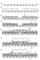
- FIG. 4 is a schematic cross-sectional view illustrating a method for manufacturing an electronic component according to one embodiment.
- FIG. 2 is a schematic cross-sectional view for explaining a joint between a metal wiring and a polymer molded body in an electronic component.
- FIG. 4 is a schematic cross-sectional view illustrating a method for manufacturing an electronic component according to one embodiment.
- 5 is an SEM image showing an example of a cross section of a metal wiring made of a sintered body of metal particles. It is a schematic diagram which shows the manufacturing method of the electronic component in an Example.
- FIG. 2 is a cross-sectional observation view of an electronic component manufactured in an example.
- FIG. 2 is a cross-sectional observation view of an electronic component manufactured in an example.
- FIG. 2 is a cross-sectional observation view of an electronic component manufactured in an example. It is a schematic diagram for explaining the measuring method of the shear strength in an example. It is a schematic diagram for explaining the measuring method of the shear strength in an example.
- FIG. 7 is a cross-sectional image diagram of an electronic component manufactured in a comparative example.
- FIG. 7 is a cross-sectional image diagram of an electronic component manufactured in a comparative example.
- the method for manufacturing an electronic component includes a first step of applying a metal paste containing metal particles in a predetermined pattern on a polymer molded body to form a metal paste layer, and sintering the metal particles. Accordingly, a second step of forming a metal wiring, a third step of applying a solder paste containing solder particles and a resin component on the metal wiring to form a solder paste layer, and A fourth step of arranging the electronic element, and forming a resin layer covering at least a part of the solder layer by heating the solder paste layer to form a solder layer for joining the metal wiring and the electronic element. 5 steps.
- the metal particles preferably contain at least one metal selected from the group consisting of copper, nickel, palladium, gold, platinum, silver and tin. Since sintering easily occurs at low temperatures, the metal particles preferably contain copper or silver, and more preferably contain copper from the viewpoint of suppressing migration when miniaturized. In consideration of firing at a low temperature and material costs, it is more preferable to use silver-coated copper particles as the metal particles.
- One kind of the metal particles may be used alone, or two or more kinds may be used in combination. Further, the metal particles may include two or more types of metal particles having different particle diameters, for example, a first metal particle having a particle diameter of 2.0 ⁇ m or more and a second metal particle having a particle diameter of 0.8 ⁇ m or less. Metal particles.
- FIG. 1 is a schematic view illustrating a method for manufacturing an electronic component according to one embodiment. The case where copper particles are used as metal particles for forming metal wiring will be described.
- a copper paste containing copper particles is applied on a polymer molded body in a predetermined pattern to form a metal (copper) paste layer (first step).
- first step first, as shown in FIG. 1A, a polymer molded body 1 is prepared (preparation step).
- the polymer molded body 1 is made of, for example, polyamide (PA), polybutylene terephthalate (PBT), polycarbonate (PC), polyetherimide (PI), polyphenylene sulfide (PPS), polyetheretherketone (PEEK), liquid crystal polymer (LCP) ) Is a molded article formed by a known method using a polymer such as The shape and size of the polymer molded article are arbitrary.
- the polymer molded body 1 is preferably made of a liquid crystal polymer (LCP) or polyphenylene sulfide (PPS).
- a copper paste is applied on the polymer molded body 1 in a predetermined pattern (to a portion where a copper wiring is to be formed), and The layer 2 is formed (forming step).
- Copper paste is, for example, screen printing, transfer printing, offset printing, jet printing, dispenser, jet dispenser, needle dispenser, comma coater, slit coater, die coater, gravure coater, slit coat, letterpress printing, intaglio printing, gravure printing, stencil It is applied by printing, soft lithography, bar coating, applicator, particle deposition method, spray coater, spin coater, dip coater, electrodeposition coating and the like.
- the thickness of the copper paste layer may be 1 ⁇ m or more, 2 ⁇ m or more, 3 ⁇ m or more, 5 ⁇ m or more, 10 ⁇ m or more, 15 ⁇ m or more, or 20 ⁇ m or more, 3000 ⁇ m or less, 1000 ⁇ m or less, 500 ⁇ m or less, 300 ⁇ m or less, 250 ⁇ m or less, 200 ⁇ m or less. , 150 ⁇ m or less, or 100 ⁇ m or less.
- the copper paste layer 2 provided on the polymer molded body 1 may be appropriately dried from the viewpoint of suppressing the flow of the copper particles during sintering and the generation of voids.
- the gas atmosphere during drying may be the air, an oxygen-free atmosphere such as nitrogen or a rare gas, or a reducing atmosphere such as hydrogen or formic acid.
- the drying method may be drying at room temperature, drying by heating, or drying under reduced pressure.
- a hot plate for example, a hot plate, a hot air dryer, a hot air heating furnace, a nitrogen dryer, an infrared dryer, an infrared heating furnace, a far infrared heating furnace, a microwave heating device, a laser heating device, an electromagnetic A heating device, a heater heating device, a steam heating furnace, a hot plate pressing device, or the like can be used.
- the drying temperature and time may be appropriately adjusted according to the type and amount of the dispersion medium used.
- the drying temperature may be, for example, 50 ° C. or higher and 180 ° C. or lower.
- the drying time may be, for example, 1 minute or more, and may be 120 minutes or less.
- the copper paste contains, as copper particles, for example, first copper particles having a particle diameter (maximum diameter) of 2.0 ⁇ m or more.
- the particle diameter (maximum diameter) of the first copper particles is 2.0 ⁇ m or more, and may be, for example, 3.0 ⁇ m or more.
- the particle size of the first copper particles may be 20 ⁇ m or less, and may be 10 ⁇ m or less.
- the average particle diameter (average maximum diameter) of the first copper particles may be not less than 1.0 ⁇ m or not less than 3 ⁇ m, and not more than 20 ⁇ m or not more than 10 ⁇ m from the viewpoint of further suppressing disconnection due to thermal stress of the obtained wiring. May be.
- the particle size and average particle size of the first copper particles can be determined, for example, from an SEM image of the particles.
- a method of calculating the particle size (maximum diameter) of the first copper particles from the SEM image will be described.
- the powder of the first copper particles is placed on a carbon tape for SEM with a spatula to form a sample for SEM. This SEM sample is observed at 5000 times with a SEM device.
- a rectangle circumscribing the first copper particle in the SEM image is drawn by image processing software, and the long side of the rectangle is defined as the particle size (maximum diameter) of the particle. Using a plurality of SEM images, this measurement is performed on 50 or more first copper particles, and the average value of the particle sizes (average maximum diameter) is calculated.
- the volume average particle diameter of the first copper particles may be 2.0 ⁇ m or more or 3.0 ⁇ m or more, and may be 50 ⁇ m or less, 20 ⁇ m or less, or 10 ⁇ m or less.
- a volume average particle diameter means 50% volume average particle diameter.
- the first copper particles are preferably in the form of flakes.
- the first copper particles are oriented substantially parallel to the copper paste application surface, volume shrinkage when the copper particles in the copper paste are sintered is suppressed, and the heat stress of the obtained wiring is reduced. Disconnection due to the above is further suppressed. Although the reason is not clear, the adhesiveness between the copper wiring and the polymer molded body is further improved.
- the aspect ratio of the first copper particles may be 4 or more, and may be 6 or more.
- the aspect ratio is within the above range, the first copper particles in the copper paste are easily oriented in parallel to the surface to which the copper paste is applied, and the volume of the copper particles in the copper paste when it is sintered Shrinkage can be suppressed. Therefore, disconnection due to thermal stress of the obtained wiring can be further suppressed.
- the aspect ratio (major axis / thickness) of the copper particles in the copper paste can be determined, for example, by observing an SEM image of the particles and measuring the major axis and the thickness.
- the copper paste preferably contains first copper particles having a particle size of 2.0 ⁇ m or more and 50 ⁇ m or less and an aspect ratio of 4 or more.
- first copper particles having a particle size of 2.0 ⁇ m or more and 50 ⁇ m or less and an aspect ratio of 4 or more.
- the copper paste may have copper particles having a particle size of 2.0 ⁇ m or more and 50 ⁇ m or less and an aspect ratio of less than 2, but have a particle size of 2.0 ⁇ m or more and 50 ⁇ m or less and an aspect ratio of less than 2.
- the content of the copper particles is preferably not more than 50 parts by mass with respect to 100 parts by mass of the first copper particles having a particle size of 2.0 ⁇ m or more and 50 ⁇ m or less and an aspect ratio of 4 or more, It is more preferable that the amount be 30 parts by mass or less.
- the content of copper particles having an average particle size of 2.0 ⁇ m or more and 50 ⁇ m or less and an aspect ratio of less than 2 is as follows: Yes, it may be 20 parts by mass or less, 10 parts by mass or less, or 0 parts by mass with respect to 100 parts by mass of the first copper particles having an aspect ratio of 4 or more.
- the content of the first copper particles in the copper paste may be 1% by mass or more, 10% by mass or more, or 20% by mass or more, based on the total mass of the metal particles contained in the copper paste, and may be 90% by mass. % Or less, 70% by weight or less, or 50% by weight or less.
- the content of the first copper particles is within the above range, it becomes easy to form a wiring having excellent conduction reliability.
- the first copper particles may be treated with a surface treatment agent from the viewpoint of dispersion stability and oxidation resistance.
- the surface treatment agent may be removed at the time of forming the wiring (when sintering the copper particles).
- the surface treating agent include aliphatic carboxylic acids such as palmitic acid, stearic acid, arachidic acid and oleic acid; aromatic carboxylic acids such as terephthalic acid, pyromellitic acid and o-phenoxybenzoic acid; cetyl alcohol and stearyl alcohol Aliphatic alcohols such as p-phenylphenol; alkylamines such as octylamine, dodecylamine and stearylamine; aliphatic nitriles such as stearonitrile and decanenitrile Silane coupling agents such as alkylalkoxysilanes; and polymer treatment agents such as polyethylene glycol, polyvinyl alcohol, polyvinylpyrrolidone, and silicone oligomers.
- the treatment amount of the surface treatment agent may be an amount of one or more molecular layers on the particle surface.
- the treatment amount of such a surface treatment agent varies depending on the specific surface area of the first copper particles, the molecular weight of the surface treatment agent, and the minimum coverage area of the surface treatment agent.
- the treatment amount of the surface treatment agent is usually 0.001% by mass or more.
- the treatment amount of the surface treatment agent is determined by the number of molecular layers (n) attached to the surface of the first copper particles, the specific surface area (A p ) (unit m 2 / g) of the first copper particles, the surface treatment agent of molecules (M s) (unit g / mol), the minimum coverage area of the surface treatment agent (S S) (unit m 2 / piece), from Avogadro's number (N a) (6.02 ⁇ 10 23 pieces) Can be calculated.
- the specific surface area of the first copper particles can be calculated by measuring the dried copper particles by a BET specific surface area measurement method.
- Minimum coverage of the surface treatment agent if the surface treatment agent is a straight-chain saturated fatty acids, is 2.05 ⁇ 10 -19 m 2/1 molecule.
- calculation from a molecular model or “Chemistry and Education” Katsuhiro Kameda, Sumio Inafuku, Iwao Mori, 40 (2), 1992, p114-117) It can be measured by the method described. An example of a method for quantifying a surface treatment agent will be described.
- the surface treating agent can be identified by a thermal desorption gas / gas chromatograph mass spectrometer of the dried powder obtained by removing the dispersion medium from the copper paste, whereby the carbon number and the molecular weight of the surface treating agent can be determined.
- the carbon content of the surface treatment agent can be analyzed by carbon content analysis. Examples of the carbon content analysis method include a high-frequency induction heating furnace combustion / infrared absorption method. From the carbon number, molecular weight and carbon content of the identified surface treatment agent, the amount of the surface treatment agent can be calculated from the above equation.
- first copper particles can be used.
- first copper particles include, for example, MA-C025 (manufactured by Mitsui Mining & Smelting Co., Ltd., average particle size: 4.1 ⁇ m), 3L3 (Fukuda Metal Foil Powder Co., Ltd., average particle size: 7.3 ⁇ m) ), 1110F (manufactured by Mitsui Kinzoku Mining Co., Ltd., average particle size: 5.8 ⁇ m), and 2L3 (Fukuda Metal Foil Powder Co., Ltd., average particle size: 9 ⁇ m).
- the first copper particles having a particle size of 2.0 ⁇ m or more and 50 ⁇ m or less and an aspect ratio of 4 or more are included, and the particle size is 2.0 ⁇ m or more and 50 ⁇ m or less, and the aspect ratio is
- the content of the copper particles that is less than 2 is 50 parts by mass or less, preferably 30 parts by mass, based on 100 parts by mass of the first copper particles having a particle size of 2.0 ⁇ m or more and 50 ⁇ m or less and an aspect ratio of 4 or more. Copper particles that are not more than parts by mass can be used. A commercial product composed of such copper particles may be selected and used.
- the copper paste may include first copper particles and second copper particles having a particle diameter (maximum diameter) of 0.8 ⁇ m or less.
- the second copper particles are interposed between the first copper particles, so that the conductivity of the obtained wiring tends to be improved.
- the first copper particles are used as the copper particles, it is preferable to use the first copper particles and the second copper particles together. That is, when a copper paste is prepared from only the second copper particles, since the volume shrinkage and sintering shrinkage accompanying the drying of the dispersion medium are large, when the copper particles are sintered, the sintered body (wiring) starts from the adhered surface.
- the second copper particles act as copper particles for suitably bonding between the first copper particles. Further, the second copper particles are more excellent in sinterability than the first copper particles, and have a function of promoting sintering of the copper particles. For example, it becomes possible to sinter the copper particles at a lower temperature than when the first copper particles are used alone.
- the particle size of the second copper particles may be 0.5 ⁇ m or less, 0.4 ⁇ m or less, or 0.3 ⁇ m or less.
- the particle size of the second copper particles may be 0.01 ⁇ m or more, 0.05 ⁇ m or more, 0.1 ⁇ m or more, or 0.2 ⁇ m or more.
- the average particle size of the second copper particles may be 0.01 ⁇ m or more, 0.05 ⁇ m or more, 0.1 ⁇ m or more, or 0.2 ⁇ m or more, 0.8 ⁇ m or less, 0.5 ⁇ m or less, 0.4 ⁇ m or less or It may be 0.3 ⁇ m or less.
- the volume average particle diameter of the second copper particles may be 0.01 ⁇ m or more and 0.8 ⁇ m or less.
- the volume average particle diameter of the second copper particles is 0.01 ⁇ m or more, effects such as suppression of the synthesis cost of the second copper particles, good dispersibility, and suppression of the amount of the surface treatment agent are easily obtained.
- the volume average particle diameter of the second copper particles is 0.8 ⁇ m or less, the effect that the sinterability of the second copper particles is excellent is easily obtained.
- the volume average particle diameter of the second copper particles may be 0.05 ⁇ m or more, 0.1 ⁇ m or more, or 0.2 ⁇ m or more, and 0.5 ⁇ m or less, 0.4 ⁇ m or less or It may be 0.3 ⁇ m or less.
- the second copper particles may contain 10% by mass or more of copper particles having a particle size of 0.01 ⁇ m or more and 0.8 ⁇ m or less.
- the second copper particles may include copper particles having a particle size of 0.01 ⁇ m or more and 0.8 ⁇ m or less, 20% by mass or more, and 30% by mass or more, It may contain 100% by mass.
- the content ratio of the copper particles having a particle diameter of 0.01 ⁇ m or more and 0.8 ⁇ m or less in the second copper particles is 20% by mass or more, the dispersibility of the copper particles is further improved, the viscosity is increased, and the paste concentration is decreased. Can be further suppressed.
- the content of the second copper particles in the copper paste is 20% by mass or more, 30% by mass or more, 35% by mass or more, or 40% by mass or more based on the total mass of the metal particles contained in the copper paste. May be 90% by mass or less, 85% by mass or less, or 80% by mass or less. When the content of the second copper particles is within the above range, disconnection due to thermal stress of the obtained wiring is less likely to occur.
- the content of the second copper particles in the copper paste may be 20% by mass or more, and 90% by mass or less, based on the total of the mass of the first copper particles and the mass of the second copper particles. Good.
- the content of the second copper particles is 20% by mass or more, the space between the first copper particles can be sufficiently filled, and the resulting wiring is less likely to be disconnected due to thermal stress.
- the content of the second copper particles is 90% by mass or less, the volume shrinkage when the copper particles are sintered can be sufficiently suppressed, so that the resulting wiring is less likely to be disconnected due to thermal stress.
- the content of the second copper particles is at least 30% by mass and at least 35% by mass based on the total mass of the first copper particles and the mass of the second copper particles. Or 40% by mass or more, or 85% by mass or less or 80% by mass or less.
- the shape of the second copper particles may be, for example, spherical, massive, needle-like, flake-like, substantially spherical, or the like.
- the second copper particles may be aggregates of copper particles having these shapes. From the viewpoints of dispersibility and filling properties, the shape of the second copper particles may be spherical, substantially spherical, or flake-like, and from the viewpoint of combustibility, and mixing properties with the first copper particles, spherical or spherical. It may be substantially spherical.
- the aspect ratio of the second copper particles may be 5 or less, or may be 3 or less from the viewpoint of dispersibility, filling properties, and mixing properties with the first copper particles.
- the second copper particles may be treated with a specific surface treatment agent.
- Specific surface treatment agents include, for example, organic acids having 8 to 16 carbon atoms. Examples of the organic acid having 8 to 16 carbon atoms include caprylic acid, methylheptanoic acid, ethylhexanoic acid, propylpentanoic acid, pelargonic acid, methyloctanoic acid, ethylheptanoic acid, propylhexanoic acid, capric acid, methylnonanoic acid, ethyl Octanoic acid, propylheptanoic acid, butylhexanoic acid, undecanoic acid, methyldecanoic acid, ethylnonanoic acid, propyloctanoic acid, butylheptanoic acid, lauric acid, methylundecanoic acid, ethyldecanoic acid, propylnonanoic acid, butylocta
- One type of organic acid may be used alone, or two or more types may be used in combination. By combining such an organic acid with the second copper particles, there is a tendency that both dispersibility of the second copper particles and desorption of the organic acid during sintering can be compatible.
- the treatment amount of the surface treatment agent may be such that the monolayer to trilayer adhere to the surface of the second copper particles.
- the treatment amount of the surface treatment agent may be 0.07% by mass or more, 0.10% by mass or more, or 0.2% by mass or more, 2.1% by mass or less, 1.6% by mass or less, or 1% by mass. 0.1 mass% or less.
- the surface treatment amount of the second copper particles can be calculated by the method described above for the first copper particles. The same applies to the specific surface area, the molecular weight of the surface treatment agent, and the minimum coating area of the surface treatment agent.
- second copper particles commercially available particles can be used.
- Commercially available second copper particles include, for example, CH-0200 (manufactured by Mitsui Kinzoku Mining Co., Ltd., volume average particle size 0.36 ⁇ m) and HT-14 (manufactured by Mitsui Kinzoku Mining Co., Ltd., volume average particle size 0) .41 ⁇ m), CT-500 (manufactured by Mitsui Kinzoku Mining Co., Ltd., volume average particle size 0.72 ⁇ m), and Tn-Cu100 (manufactured by Taiyo Nissin Co., Ltd., volume average particle size 0.12 ⁇ m).
- the total of the content of the first copper particles and the content of the second copper particles in the copper paste may be 80% by mass or more based on the total mass of the metal particles contained in the copper paste. If the total of the content of the first copper particles and the content of the second copper particles is within the above range, disconnection of the obtained wiring due to thermal stress is less likely to occur. From the viewpoint of exhibiting the above effect even more, the total content of the first copper particles and the content of the second copper particles may be 90% by mass or more based on the total mass of the metal particles, It may be 95% by mass or more, or 100% by mass.
- the copper paste may further include other metal particles other than the copper particles.
- Other metal particles include, for example, particles of nickel, silver, gold, palladium, platinum and the like.
- the volume average particle size of the other metal particles may be 0.01 ⁇ m or more or 0.05 ⁇ m or more, and may be 10 ⁇ m or less, 5.0 ⁇ m or less, or 3.0 ⁇ m or less.
- the content may be less than 20% by mass, based on the total mass of the metal particles contained in the copper paste, from the viewpoint of obtaining sufficient bonding properties. It may be as follows.
- Other metal particles may not be included.
- the shape of other metal particles is not particularly limited.
- metal particles other than copper particles By including metal particles other than copper particles, it is possible to obtain wiring in which a plurality of types of metals are dissolved or dispersed, so that mechanical properties such as wiring yield stress and fatigue strength are improved and conduction reliability is improved. Easy to improve. Further, by adding a plurality of types of metal particles, the bonding strength of the formed wiring to a specific adherend (for example, LCP) is easily improved, and the conduction reliability is easily improved.
- a specific adherend for example, LCP
- the dispersion medium contained in the copper paste is not particularly limited, and may be, for example, a volatile medium.
- the volatile dispersion medium include monohydric and polyhydric alcohols such as pentanol, hexanol, heptanol, octanol, decanol, ethylene glycol, diethylene glycol, propylene glycol, butylene glycol, ⁇ -terpineol, and isobornylcyclohexanol.
- Ethylene glycol butyl ether ethylene glycol phenyl ether, diethylene glycol methyl ether, diethylene glycol ethyl ether, diethylene glycol butyl ether, diethylene glycol isobutyl ether, diethylene glycol hexyl ether, triethylene glycol methyl ether, diethylene glycol dimethyl ether, diethylene glycol diethyl ether, diethylene glycol dibutyl ether Diethylene glycol butyl methyl ether, diethylene glycol isopropyl methyl ether, triethylene glycol dimethyl ether, triethylene glycol butyl methyl ether, propylene glycol propyl ether, dipropylene glycol methyl ether, dipropylene glycol ethyl ether, dipropylene glycol propyl ether, dipropylene glycol Ethers such as butyl ether, dipropylene glycol dimethyl ether, tripropylene glycol methyl ether, and tripropy
- Examples of mercaptans having an alkyl group having 1 to 18 carbon atoms include ethyl mercaptan, n-propyl mercaptan, i-propyl mercaptan, n-butyl mercaptan, i-butyl mercaptan, t-butyl mercaptan, pentyl mercaptan, hexyl mercaptan And dodecyl mercaptan.
- Examples of mercaptans having a cycloalkyl group having 5 to 7 carbon atoms include cyclopentyl mercaptan, cyclohexyl mercaptan, and cycloheptyl mercaptan.
- the content of the dispersion medium may be 5 parts by mass or more, and may be 50 parts by mass or less, with the total mass of the metal particles contained in the copper paste being 100 parts by mass.
- the content of the dispersion medium is within the above range, the viscosity of the copper paste can be adjusted to a more appropriate one, and sintering of the copper particles is hardly hindered.
- a wetting improver such as a nonionic surfactant or a fluorine surfactant; an antifoaming agent such as silicone oil; an ion trapping agent such as an inorganic ion exchanger is appropriately added. Is also good.
- the copper paste described above can be prepared by mixing copper particles and optional components (additives, other metal particles, etc.) in a dispersion medium. After mixing the components, a stirring process may be performed. The maximum diameter of the dispersion may be adjusted by a classification operation.
- the copper paste is prepared by previously mixing the second copper particles, the surface treating agent, and the dispersion medium, performing a dispersion treatment to prepare a dispersion of the second copper particles, and further mixing the first copper particles and other metal particles. And an optional additive.
- the dispersibility of the second copper particles is improved, the mixing property with the first copper particles is improved, and the performance of the copper paste is further improved.
- Aggregates may be removed by subjecting the dispersion of the second copper particles to a classification operation.
- the copper wiring 3 is formed by sintering the copper particles.
- the heating treatment includes, for example, a hot plate, a hot air dryer, a hot air heating furnace, a nitrogen dryer, an infrared dryer, an infrared heating furnace, a far infrared heating furnace, a microwave heating device, a laser heating device, an electromagnetic heating device, Heating means such as a heater heating device and a steam heating furnace can be used.
- the atmosphere during sintering may be an oxygen-free atmosphere from the viewpoint of suppressing oxidation of the sintered body, and may be a reducing atmosphere from the viewpoint of removing surface oxides of copper particles in the copper paste layer 2.
- the oxygen-free atmosphere includes, for example, introduction of an oxygen-free gas such as nitrogen or a rare gas, or under vacuum.
- the reducing atmosphere include pure hydrogen gas, a mixed gas of hydrogen and nitrogen represented by a forming gas, nitrogen in formic acid gas, mixed gas of hydrogen and rare gas, and rare gas containing formic acid gas. No.
- the highest temperature reached during the heat treatment may be 150 ° C. or higher, and may be 350 ° C. or lower, 300 ° C. or lower, or 260 ° C. or lower, from the viewpoint of reducing thermal damage to each member and improving the yield. . If the maximum temperature reached is 150 ° C. or higher, the sintering tends to proceed sufficiently when the maximum temperature holding time is 60 minutes or less.
- the attained maximum temperature holding time may be 1 minute or more, and may be 60 minutes or less, 40 minutes or less, or 30 minutes or less from the viewpoint of volatilizing all of the dispersion medium and improving the yield.
- the copper content (volume ratio) in the copper wiring 3 is preferably 65% by volume or more, more preferably 70% by volume or more, even more preferably 80% by volume or more based on the total volume of the copper wiring. By setting the copper content in the copper wiring 3 to 65% by volume or more, good conduction reliability can be obtained.
- the content (volume ratio) of copper in the copper wiring 3 is preferably 95% by volume or less based on the total volume of the copper wiring. In this case, the copper wiring 3 has a gap. Since the copper wiring 3 has an appropriate gap, when a solder paste containing a resin component is applied to the surface of the copper wiring 3 opposite to the surface in contact with the polymer molded body 1, the resin component is filled in the space inside the copper wiring 3.
- the resin also reaches and cures in the voids 3a between the copper wiring 3 and the copper molded body 3 in contact with the polymer molded body, thereby further improving the adhesive strength between the polymer molded body 1 and the copper wiring 3.
- the copper wiring 3 may have a copper element ratio of 95% by mass or more, 97% by mass or more, or 98% by mass or more in the elements other than the light elements among the constituent elements. And may be 100% by mass.
- the above ratio of the copper element in the copper wiring 3 is within the above range, formation of an intermetallic compound or precipitation of a different element at the metal copper crystal grain boundary can be suppressed, and the properties of the metal copper constituting the copper wiring 3 are reduced. It is easy to be strong and more excellent connection reliability is easily obtained.
- the ratio of the copper element in the elements other than the light elements in the copper wiring 3 is 100% by mass, the volume ratio of the copper can be regarded as the density (%).
- the copper wiring 3 may include a structure derived from first copper particles oriented substantially parallel to a bonding interface with the polymer molded body 1 (for example, a bonding surface between the polymer molded body 1 and the copper wiring 3). preferable. In this case, by orienting the first particles substantially parallel to the polymer molded body 1, cracks in the copper wiring 3 formed by sintering can be suppressed. Further, although the reason is not clear, the adhesiveness between the copper wiring 3 formed by sintering and the polymer molded body 1 can be improved.
- solder paste containing the solder particles 4 and the resin component 5 is applied on the copper wiring 3 in a predetermined pattern to form a solder paste layer 6.
- Part of the resin component 5 penetrates into the voids 3 a of the copper wiring 3 to form a resin filled portion 7 that fills at least a part of the copper wiring 3.
- the particle size of the solder particles 4 may be, for example, 0.4 to 30 ⁇ m, 0.5 to 20 ⁇ m, or 0.6 to 15 ⁇ m.
- the particle size of the solder particles 4 is 0.4 ⁇ m or more, it is hard to be affected by the oxidation of the solder surface, and the conduction reliability is easily improved.
- the particle size of the solder particles 4 is 30 ⁇ m or less, it is easy to improve insulation reliability.
- the particle size of the solder particles 4 can be measured by observation using a scanning electron microscope (SEM). That is, the average particle size of the solder particles can be obtained by measuring the particle size of 300 arbitrary solder particles by observation using an SEM and taking the average value thereof.
- SEM scanning electron microscope
- the solder particles 4 contain tin.
- the solder particles 4 include at least one selected from the group consisting of an In—Sn alloy, an In—Sn—Ag alloy, a Sn—Bi alloy, a Sn—Bi—Ag alloy, a Sn—Ag—Cu alloy, and a Sn—Cu alloy.
- a tin alloy may be used.
- tin alloy for example, In—Sn (In 52% by mass, Bi 48% by mass, melting point 118 ° C.), In—Sn—Ag (In 20% by mass, Sn 77.2% by mass, Ag 2.8% by mass, melting point 175 ° C.) , Sn-Bi (Sn 43% by mass, Bi 57% by mass, melting point 138 ° C), Sn-Bi-Ag (Sn 42% by mass, Bi 57% by mass, Ag 1% by mass, melting point 139 ° C) Sn-Ag-Cu (Sn96.5% by mass) %, Ag 3 mass%, Cu 0.5 mass%, melting point 217 ° C.) and Sn—Cu (Sn 99.3 mass%, Cu 0.7 mass%, melting point 227 ° C.).
- a tin alloy can be selected according to the joining temperature. For example, when a tin alloy having a low melting point, such as an In—Sn alloy or a Sn—Bi alloy, is used, bonding can be performed at 150 ° C. or lower. When a tin alloy having a high melting point, such as Sn—Ag—Cu or Sn—Cu, is used, high reliability tends to be achieved even after being left at a high temperature.
- the tin alloy constituting the solder particles 4 may include at least one selected from Ag, Cu, Ni, Bi, Zn, Pd, Pb, Au, P and B.
- Ag or Cu may be contained from the following viewpoints. That is, when the solder particles 4 contain Ag or Cu, the melting point of the solder particles can be reduced to about 220 ° C., and the effect of obtaining good conduction reliability by improving the bonding strength with the electrode can be obtained. Is played.
- the Cu content of the solder particles 4 may be, for example, 0.05 to 10% by mass, 0.1 to 5% by mass, or 0.2 to 3% by mass.
- the Cu content is 0.05% by mass or more, good solder connection reliability is easily obtained, and when the Cu content is 10% by mass or less, the melting point of the solder particles becomes low and the solder wettability is improved. As a result, the connection reliability of the joint tends to be good.
- the Ag content of the solder particles 4 may be, for example, 0.05 to 10% by mass, 0.1 to 5% by mass, or 0.2 to 3% by mass.
- the Ag content is 0.05% by mass or more, good solder connection reliability is easily obtained.
- the Ag content is 10% by mass or less, the melting point is lowered and the solder wettability is improved. Is likely to have good connection reliability.
- the resin component 5 may contain a thermosetting compound.
- the thermosetting compound include oxetane compounds, epoxy compounds, episulfide compounds, (meth) acryl compounds, phenol compounds, amino compounds, unsaturated polyester compounds, polyurethane compounds, silicone compounds, and polyimide compounds.
- an epoxy compound is preferable from the viewpoint of further improving the curability and viscosity of the resin component and further enhancing the adhesiveness between the polymer molded body 1 and the copper wiring 3.
- the resin component 5 may further include a thermosetting agent.
- the thermal curing agent include an imidazole curing agent, an amine curing agent, a phenol curing agent, a polythiol curing agent, an acid anhydride, a thermal cation initiator, and a thermal radical generator.
- the thermosetting agent one type may be used alone, or two or more types may be used in combination.
- An imidazole curing agent, a polythiol curing agent, or an amine curing agent is preferable because it can be rapidly cured at a low temperature.
- a latent thermosetting agent may be used as the thermosetting agent in order to enhance the storage stability when the thermosetting compound and the thermosetting agent are mixed.
- the latent heat curing agent is a latent imidazole curing agent, a latent polythiol curing agent, or a latent amine curing agent.
- the thermosetting agent may be coated with a polymer such as a polyurethane resin or a polyester resin.
- imidazole curing agent examples include 2-methylimidazole, 2-ethyl-4-methylimidazole, 1-cyanoethyl-2-phenylimidazole, 1-cyanoethyl-2-phenylimidazolium trimellitate, and 2,4-diamino- 6- [2′-Methylimidazolyl- (1 ′)]-ethyl-s-triazine and 2,4-diamino-6- [2′-methylimidazolyl- (1 ′)]-ethyl-s-triazine isocyanuric acid addition Things.
- Polythiol curing agents include, for example, trimethylolpropane tris-3-mercaptopropionate, pentaerythritol tetrakis-3-mercaptopropionate and dipentaerythritol hexa-3-mercaptopropionate.
- the solubility parameter of the polythiol curing agent is preferably 9.5 or more, preferably 12 or less. Solubility parameters are calculated by the Fedors method. For example, the solubility parameter of trimethylolpropane tris-3-mercaptopropionate is 9.6 and that of dipentaerythritol hexa-3-mercaptopropionate is 11.4.
- amine curing agent examples include hexamethylenediamine, octamethylenediamine, decamethylenediamine, 3,9-bis (3-aminopropyl) -2,4,8,10-tetraspiro [5.5] undecane, bis ( 4-aminocyclohexyl) methane, metaphenylenediamine and diaminodiphenylsulfone.
- thermal cationic curing agent examples include an iodonium-based cationic curing agent, an oxonium-based cationic curing agent, and a sulfonium-based cationic curing agent.
- examples of the iodonium-based cationic curing agent include bis (4-tert-butylphenyl) iodonium hexafluorophosphate.
- Examples of the oxonium-based cationic curing agent examples include trimethyloxonium tetrafluoroborate.
- the sulfonium-based cationic curing agent examples include tri-p-tolylsulfonium hexafluorophosphate.
- thermal radical generator examples include an azo compound and an organic peroxide.
- examples of the azo compound include azobisisobutyronitrile (AIBN).
- Organic peroxides include, for example, di-tert-butyl peroxide and methyl ethyl ketone peroxide.
- the resin component 5 may further contain a flux.
- the flux melts the oxide on the solder surface, fuses the particles, and improves the solder wettability to the copper wiring 3.
- a flux generally used for soldering or the like can be used.
- the flux include zinc chloride, a mixture of zinc chloride and an inorganic halide, a mixture of zinc chloride and an inorganic acid, a molten salt, phosphoric acid, a derivative of phosphoric acid, an organic halide, hydrazine, an organic acid, and rosin.
- One type of flux may be used alone, or two or more types may be used in combination.
- Examples of the molten salt include ammonium chloride.
- Organic acids include, for example, lactic acid, citric acid, stearic acid, glutamic acid and glutaric acid.
- Examples of rosin include activated rosin and non-activated rosin.
- Pine resin is a rosin containing abietic acid as a main component.
- the melting point of the flux is preferably 50 ° C. or higher, more preferably 70 ° C. or higher, and further preferably 80 ° C. or higher.
- the melting point of the flux is preferably 200 ° C. or lower, more preferably 160 ° C. or lower, further preferably 150 ° C. or lower, and particularly preferably 140 ° C. or lower.
- the range of the melting point of the flux is preferably from 80 to 190 ° C, and more preferably from 80 to 140 ° C.
- Examples of the flux having a melting point in the range of 80 to 190 ° C. include succinic acid (melting point 186 ° C.), glutaric acid (melting point 96 ° C.), adipic acid (melting point 152 ° C.), pimelic acid (melting point 104 ° C.), suberic acid (Melting point: 142 ° C.), benzoic acid (melting point: 122 ° C.), and malic acid (melting point: 130 ° C.).
- the electronic element 8 includes a power module including a diode, a rectifier, a thyristor, a MOS gate driver, a power switch, a power MOSFET, an IGBT, a Schottky diode, a fast recovery diode, a transmitter, an amplifier, an LED module, a capacitor, a gyro sensor, and the like. Is mentioned.
- Examples of a method for disposing the electronic element 8 on the solder paste layer 6 include a method using a chip mounter, a flip chip bonder, a positioning jig made of carbon or ceramics, or the like.
- the electrode 9 may be an electrode containing at least one metal selected from the group consisting of copper, nickel, palladium, gold, platinum, silver and tin on its outermost surface. Also, from the viewpoint that an impurity (intermetallic compound) is not formed between the solder layer 11 and the electrode 9 and mounting with high bonding reliability can be performed, preferably, it is selected from the group consisting of copper, nickel and palladium. An electrode containing at least one metal on the outermost surface.
- the electrode 9 may be composed of a single or multiple metal-containing layers containing these metals.
- the heating treatment includes, for example, a hot plate, a hot air dryer, a hot air heating furnace, a nitrogen dryer, an infrared dryer, an infrared heating furnace, a far infrared heating furnace, a microwave heating device, a laser heating device, an electromagnetic heating device, Heating means such as a heater heating device and a steam heating furnace can be used.
- a resin layer is formed by melting the solder particles 4 to form a solder layer 11, joining the copper wiring 3 and the electrode 9 of the electronic element 8, and curing the resin component 5 to cover at least a part of the solder layer 11.
- 12 is formed. Specifically, taking Sn-Bi (Sn: 43% by mass, Bi: 57% by mass) having a melting point of 138 ° C. as an example, the solder layer is formed by holding at 150 ° C. It is preferable that the resin layer 12 is cured by covering the outer periphery of the resin layer. At this time, the resin component filled in at least a part of the void 3a of the copper wiring 3 is cured to form the resin filled portion 13.
- the atmosphere at the time of solder joining may be an oxygen-free atmosphere from the viewpoint of suppressing oxidation of the sintered body, and may be a reducing atmosphere from the viewpoint of removing surface oxides of the copper wiring 3.
- the oxygen-free atmosphere includes, for example, introduction of an oxygen-free gas such as nitrogen or a rare gas, or under vacuum.
- the reducing atmosphere include pure hydrogen gas, a mixed gas of hydrogen and nitrogen represented by a forming gas, nitrogen in formic acid gas, mixed gas of hydrogen and rare gas, and rare gas containing formic acid gas. No.
- the highest temperature reached during the heat treatment may be 150 ° C. or higher, and may be 350 ° C. or lower, 300 ° C. or lower, or 260 ° C. or lower, from the viewpoint of reducing thermal damage to each member and improving the yield. . If the ultimate temperature is 150 ° C. or higher, the melting of the solder particles 4 tends to proceed sufficiently when the ultimate temperature holding time is 60 minutes or less.
- the soldering may be performed while applying pressure to the electronic element 8, or may be performed only by the weight of the electronic element 8 and other members on the solder paste layer 6.
- the pressure may be 0.01 MPa or less or 0.005 MPa or less. If the pressure applied during sintering is within the above range, no special pressurizing device is required, and the reduction in voids, the joining strength, and the connection reliability can be further improved without impairing the yield.
- a method of applying pressure to the electronic element 8 for example, a method of placing a weight on the uppermost electronic element 8 and the like can be mentioned.
- the electronic component 10 obtained by the manufacturing method described above includes a polymer molded body 1, a copper wiring 3 provided on the polymer molded body 1, a solder layer 11 for joining the copper wiring 3 and the electronic element 8, And a resin layer 12 covering at least a part of the layer 11. At least a part of the void 3 a of the copper wiring 3 is filled with a cured product of the same resin component as the resin layer 12.
- FIG. 2 is a diagram illustrating details of a joint between the copper wiring 3 and the polymer molded body 1 in the electronic component 10.
- a void 3a of the copper wiring 3 is formed at the interface with the polymer molded body 1, and the void 3a is filled with a resin component and cured to form a resin-filled part 13, and the adhesiveness between the copper wiring 3 and the polymer molded body 1 Can be improved.
- FIG. 3 is a schematic cross-sectional view illustrating a method for manufacturing an electronic component according to another embodiment.
- a polymer molded body 1 is prepared (preparation step).
- a copper paste is applied on the polymer molded body 1 in a predetermined pattern (to a portion where a copper wiring is to be formed) to form a copper paste.
- the layer 2 is formed (forming step).
- the copper wiring 3 is formed by sintering the copper particles. (Second step).
- a resin layer 14 containing a resin component is formed on a part of the copper wiring 3.
- the resin component is filled into at least a part of the void 3a of the copper wiring 3 to obtain the resin filled portion 15.
- the resin component may be the same as the resin component 5 of the solder paste described above.
- the resin layer 14 may be applied to the entire surface of the copper wiring 3 and the polymer molded body 1.
- a solder paste containing the solder particles 4 and the resin component 5 may be applied on the upper portion of the resin layer 14 applied on the copper wiring 3.
- the resin layer 14 may be formed in a portion other than the copper wiring 3 to which the electronic element 8 is joined, and may or may not be cured in advance.
- the atmosphere at the time of curing the resin layer 14 may be an oxygen-free atmosphere or a reducing atmosphere from the viewpoint of suppressing oxidation of the copper wiring 3.
- the oxygen-free atmosphere includes, for example, introduction of an oxygen-free gas such as nitrogen or a rare gas, or under vacuum.
- Examples of the reducing atmosphere include pure hydrogen gas, a mixed gas of hydrogen and nitrogen represented by a forming gas, nitrogen in formic acid gas, mixed gas of hydrogen and rare gas, and rare gas containing formic acid gas. No.
- a solder paste is applied on a predetermined copper wiring 3 in a predetermined pattern (third step).
- the resin component 5 penetrates into the voids 3 a of the copper wiring 3 and fills at least a part of the copper wiring 3.
- the electronic element 8 having the electrode 9 is arranged (mounted) at a predetermined position of the solder paste layer 6 (fourth step).
- the solder particles 4 are melted to form a solder layer 11, and the copper wiring 3 and the electrode 9 of the electronic element 8 are joined ( Fifth step).
- the resin layer 14 is cured to form the resin layer 16. Thereby, the electronic component 18 is obtained.
- the electronic component 18 obtained by the manufacturing method described above includes the polymer molded body 1, the copper wiring 3 provided on the polymer molded body 1, and the solder layer 11 for joining the copper wiring 3 and the electrode 9 of the electronic element 8. And a resin layer 12 covering at least a part of the solder layer 11 and a resin layer 16 covering a part of the copper wiring 3. At least a part of the void 3a of the copper wiring 3 is filled with a cured product of the same resin component as the resin layer 12 or the resin layer 16.
- the copper paste is applied in a predetermined pattern (a pattern corresponding to the copper wiring 3), a polymer containing a catalyst is not required, and laser irradiation and electroless copper plating are not required. Step can be omitted.
- the electronic element 8 is arranged and heat-treated, so that the copper wiring 3 and the electronic element 8 are joined to each other by soldering, At least a portion of the solder layer 11 is covered with the resin layer 12, and the resin component filled in at least a portion of the void portion of the copper wiring 3 is cured to form the resin filled portion 13 or the resin filled portion 17.
- the adhesiveness between the polymer molded body and the copper wiring can be improved.
- the electronic element 8 and the copper wiring 3 are formed by making the resin layer 14 containing the resin component covering a part of the copper wiring 3 and the resin component 5 in the solder paste the same component. And the formation of the surface protection film of the copper wiring 3 can be performed in the same step, and the conventional steps (the step of forming the solder resist (the formation of the organic film on the front surface of the copper wiring and the polymer molded body) can be performed.
- the formation of openings for solder bonding by application, exposure, and development), the application of solder paste to the wiring openings, and the soldering process by heat treatment (component mounting) Time can be shortened.
- FIG. 4 is an SEM image showing an example of a cross section of a copper wiring made of a sintered body of copper particles.
- the copper wiring 24 shown in FIG. 4 has a structure derived from flake-shaped copper particles oriented substantially parallel to a bonding interface (for example, a bonding surface between the polymer molded body and the wiring).
- a bonding interface for example, a bonding surface between the polymer molded body and the wiring.
- the breakage of the wiring can be suppressed by orienting the flake-shaped copper particles substantially parallel to the bonding interface direction.
- the adhesiveness between the wiring and the polymer molded body can be improved.
- the wiring having the copper wiring 24 shown in FIG. 4 includes, in addition to the sintered copper 24a derived from the flake-shaped copper particles, the copper particles (for example, spherical copper particles) that join the voids 24b and the flake-shaped copper particles. ) And sintered copper derived from the above.
- the wiring having the copper wiring 24 is formed, for example, by sintering a copper paste containing flake-shaped copper particles and, in some cases, copper particles (for example, spherical copper particles) that join the flake-shaped copper particles to each other. Can be formed.
- the flake shape includes a plate-like shape such as a plate-like shape and a scale-like shape.
- the ratio between the major axis (maximum diameter) and the thickness (major axis / thickness, aspect ratio) may be 5 or more.
- the number average diameter of the major axis may be 2.0 ⁇ m or more, 3.0 ⁇ m or more, or 4.0 ⁇ m or more.
- the major axis and the thickness of the sintered copper 24a derived from the flake-shaped copper particles can be determined, for example, from an SEM image of a cross section of the wiring.
- a method of measuring the major axis and the thickness of the sintered copper derived from the flaky copper particles from the SEM image will be exemplified.
- the wiring is cut into a rectangular parallelepiped shape to obtain a measurement sample.
- the sample is placed in a casting cup, and the epoxy casting resin is poured into the cup so that the entire sample is embedded and cured.
- the cast sample is cut near the cross section to be observed, the cross section is cut by polishing, and the cross section polisher (CP) processing is performed.
- CP cross section polisher
- the cross section of the sample is observed at a magnification of 5000 with a SEM device.
- the length of the longest diameter is 1.0 ⁇ m or more and the ratio of the longest diameter / thickness is 4
- the above is regarded as sintered copper derived from flake-shaped copper particles, and the major axis and thickness of sintered copper derived from flake-shaped copper particles are measured by image processing software having a length measuring function.
- the average value can be obtained by calculating a number average at 20 or more points selected at random.
- the mode using copper particles as the metal particles is described, but the metal particles according to the present embodiment are not limited to copper particles. Particles containing a sinterable metal can be used. Even when metal particles other than copper particles are used, the above-described electronic component manufacturing process can be applied.
- Copper paste a1 5.2 g of ⁇ -terpineol (manufactured by Fujifilm Wako Pure Chemical Industries, Ltd.) and 6.8 g of isobornylcyclohexanol (manufactured by Nippon Terpen Chemical Co., Ltd.) as dispersion media, and “CH-0200” (Mitsui Mitsui) as submicro copper particles Metallic Mining Co., Ltd., 50% volume average particle diameter: 0.36 ⁇ m, content of copper particles having a particle diameter of 0.01 to 0.8 ⁇ m: 95% by mass) and 52.8 g were mixed in a poly bottle.
- the dispersion was processed at 19.6 kHz and 600 W for 1 minute using a sonic homogenizer (trade name “US-600” manufactured by Nippon Seiki Co., Ltd.) to obtain a dispersion.
- a sonic homogenizer trade name “US-600” manufactured by Nippon Seiki Co., Ltd.
- 35.2 g of “MA-C025” manufactured by Mitsui Mining & Smelting Co., Ltd., content of copper particles having a maximum diameter of 1 to 20 ⁇ m: 100% by mass
- a spatula was used. Stir until dry powder is gone.
- the poly bottle was sealed, and the mixture was stirred at 2,000 rpm for 2 minutes using a rotation and revolution type stirrer (trade name “Planetary Vacuum Mixer ARV-310” manufactured by Sinky Co., Ltd.), and stirred at 2,000 rpm for 2 minutes under reduced pressure.
- a copper paste a1 was obtained.
- solder paste 25 parts by mass of solder particles (“Sn42-Bi58 particles”, average particle diameter: 20 ⁇ m) and 25 parts of bisphenol F type epoxy resin (trade name “YDF-170” manufactured by Nippon Steel & Sumikin Chemical Co., Ltd., epoxy equivalent: 170). 2 parts by mass, 1.3 parts by mass of an imidazole compound (trade name "2PZ-CN” manufactured by Shikoku Chemicals Co., Ltd.) and 3.5 parts by mass of 2,2-bishydroxymethylpropionic acid were mixed, and solder paste was used. Was prepared.
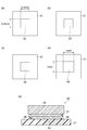
- Example 1 (Production of electronic component 40) A polymer molded article made of a liquid crystal polymer having a size of 40 mm ⁇ 40 mm and a thickness of 3 mm (“Sumica Super LCP E6000HF” manufactured by Sumitomo Chemical Co., Ltd.) was prepared. Subsequently, as shown in FIG. 5A, a stainless metal mask (thickness: 50 ⁇ m) having two rectangular openings of 1.5 mm ⁇ 1 mm is placed on the polymer molded body 31, and a metal squeegee is placed thereon. The member in which the copper paste a1 was applied by the stencil printing used to form the copper paste layer 32 was obtained.
- a stainless metal mask thickness: 50 ⁇ m
- the above-mentioned members were set in a tube furnace (manufactured by ABC), and argon gas was supplied at a flow rate of 1 L / min to replace air with argon gas. Thereafter, the copper paste layer 32 is sintered by performing a sintering process at a temperature rise of 10 minutes and a temperature of 180 ° C. for 60 minutes while flowing hydrogen gas at a flow rate of 300 mL / min. As shown in FIG. Copper wiring 33 was formed.
- a solder paste is applied on the copper wiring 33 to form a solder paste layer 34, and then, as shown in FIG. A member on which a ceramic capacitor 35 (2 mm ⁇ 1.2 mm ⁇ 0.6 mmt, trade name “GQM series” manufactured by Murata Manufacturing Co., Ltd.) on which the electrode 36 was formed was disposed (mounted) thereon.
- the electrodes 36 were formed of copper at both ends of the ceramic capacitor 35.
- FIG. 5E shows a cross-sectional shape of the electronic component 40.
- FIG. 5E is a cross-sectional view along the line IVc-IVc in FIG. 5D.
- the electrode 36 of the ceramic capacitor 35 and the copper wiring 33 were joined by a solder layer 37, and the outer periphery of the solder joint was reinforced by a resin layer 38.
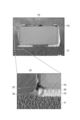
- FIG. 6 shows the result of observing the cross section of the electronic component 40 with an optical microscope.
- the electrode 36 of the ceramic capacitor 35 and the copper wiring 33 are joined via a solder layer 37, and a resin layer 38 is formed on the outer periphery of the solder layer 37.
- FIG. 7 shows the observation results of the cross sections of the polymer molded body 31, the copper wiring 33, and the solder layer 37 by an optical microscope.
- the copper wiring 33 has a gap, and the gap is filled with a resin component to form a resin filled portion 43.
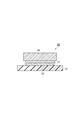
- connection strength (shear strength) of the electronic component 40 was measured using a bond tester (trade name: Universal Bond Tester Series 4000, manufactured by Dage). More specifically, as shown in FIGS. 10A and 10B, the share tool 45 is arranged at a share height of 50 ⁇ m with respect to the electronic component 40, and the speed is 0.5 mm / min in the direction of the arrow. Was used to measure the shear strength.
- FIG. 10B is a cross-sectional view taken along the line IVc-IVc in FIG. 5D.
- the adhesiveness between the polymer molded body 31 and the copper wiring 33 was evaluated from the average value of the shear strength at 20 places where the polymer molded body 31 and the copper wiring 33 were joined. Table 1 shows the results.
- FIG. 8C a solder paste was applied on the copper wiring to form a solder paste layer 34.
- a copper substrate 39 (1 mm ⁇ 1 mm ⁇ 0.3 mmt) was placed (mounted) on the solder paste layer 34 to obtain a member.
- the member shown in FIG. 8D was placed on a hot plate heated to 170 ° C. in the air and left for 15 minutes.
- FIG. 8E shows a cross-sectional shape of the electronic component 44 obtained by leaving it to stand.
- the copper substrate 39 and the copper wiring 33 were joined by the solder layer 37, and the outer periphery of the solder layer 37 was reinforced by the resin layer 38.
- FIG. 9 shows the observation result of the cross section of the electronic component 44 by an optical microscope.
- a copper substrate 39 and a copper wiring 33 are joined via a solder layer 37, and a resin layer 38 is formed on the outer periphery of the solder layer 37.
- connection strength (shear strength) of the electronic component 44 was measured using a bond tester. Specifically, as shown in FIG. 11, a share tool 45 is arranged at a share height of 50 ⁇ m with respect to the electronic component 44, and the share is performed at a speed of 0.5 mm / min in the direction of the arrow to reduce the share strength. It was measured.
- the adhesiveness between the polymer molded body 31 and the copper wiring 33 was evaluated from the average value of the shear strength at 20 places where the polymer molded body 31 and the copper wiring 33 were joined. Table 1 shows the results.
- Example 2 Electronic components 40 and 44 were produced in the same manner as in Example 1 except that the sintering temperature of the copper paste layer 32 was changed from 180 ° C. to 225 ° C., and the adhesiveness was evaluated.
- Example 3 An electronic component 40 was manufactured in the same manner as in Example 1 except that a copper paste layer 32 was formed using a copper paste a2 instead of the copper paste a1, and the copper paste layer 32 was baked at 180 ° C. for 10 minutes in the air. And the electronic component 44 was produced and adhesiveness was evaluated.
Landscapes
- Engineering & Computer Science (AREA)
- Manufacturing & Machinery (AREA)
- Mechanical Engineering (AREA)
- Microelectronics & Electronic Packaging (AREA)
- Chemical & Material Sciences (AREA)
- Materials Engineering (AREA)
- Composite Materials (AREA)
- Organic Chemistry (AREA)
- Metallurgy (AREA)
- Powder Metallurgy (AREA)
- Conductive Materials (AREA)
- Electric Connection Of Electric Components To Printed Circuits (AREA)
- Manufacturing Of Printed Wiring (AREA)
- Wire Bonding (AREA)
- Non-Metallic Protective Coatings For Printed Circuits (AREA)
- Fixed Capacitors And Capacitor Manufacturing Machines (AREA)
- Materials For Photolithography (AREA)
- Thermistors And Varistors (AREA)
Abstract
Priority Applications (6)
| Application Number | Priority Date | Filing Date | Title |
|---|---|---|---|
| EP19859807.0A EP3852507A4 (fr) | 2018-09-14 | 2019-09-05 | Composant électronique et procédé de fabrication de composant électronique |
| US17/274,788 US12070800B2 (en) | 2018-09-14 | 2019-09-05 | Electronic component and method for manufacturing electronic component |
| CN201980058937.5A CN112673715B (zh) | 2018-09-14 | 2019-09-05 | 电子零件及电子零件的制造方法 |
| JP2020545975A JP7551497B2 (ja) | 2018-09-14 | 2019-09-05 | 電子部品及び電子部品の製造方法 |
| JP2024004604A JP7708228B2 (ja) | 2018-09-14 | 2024-01-16 | 電子部品及び電子部品の製造方法 |
| US18/770,661 US20240383035A1 (en) | 2018-09-14 | 2024-07-12 | Electronic component and method for manufacturing electronic component |
Applications Claiming Priority (2)
| Application Number | Priority Date | Filing Date | Title |
|---|---|---|---|
| JP2018-172332 | 2018-09-14 | ||
| JP2018172332 | 2018-09-14 |
Related Child Applications (2)
| Application Number | Title | Priority Date | Filing Date |
|---|---|---|---|
| US17/274,788 A-371-Of-International US12070800B2 (en) | 2018-09-14 | 2019-09-05 | Electronic component and method for manufacturing electronic component |
| US18/770,661 Division US20240383035A1 (en) | 2018-09-14 | 2024-07-12 | Electronic component and method for manufacturing electronic component |
Publications (1)
| Publication Number | Publication Date |
|---|---|
| WO2020054581A1 true WO2020054581A1 (fr) | 2020-03-19 |
Family
ID=69777622
Family Applications (1)
| Application Number | Title | Priority Date | Filing Date |
|---|---|---|---|
| PCT/JP2019/035039 Ceased WO2020054581A1 (fr) | 2018-09-14 | 2019-09-05 | Composant électronique et procédé de fabrication de composant électronique |
Country Status (6)
| Country | Link |
|---|---|
| US (2) | US12070800B2 (fr) |
| EP (1) | EP3852507A4 (fr) |
| JP (2) | JP7551497B2 (fr) |
| CN (1) | CN112673715B (fr) |
| TW (1) | TWI818074B (fr) |
| WO (1) | WO2020054581A1 (fr) |
Cited By (4)
| Publication number | Priority date | Publication date | Assignee | Title |
|---|---|---|---|---|
| JP2022002302A (ja) * | 2020-06-22 | 2022-01-06 | 旭化成株式会社 | 金属配線を含む構造体及びその製造方法 |
| JP2022022600A (ja) * | 2020-06-29 | 2022-02-07 | 昭和電工マテリアルズ株式会社 | 導電部材及びその製造方法、並びに、半導体装置 |
| JP2022033596A (ja) * | 2020-08-17 | 2022-03-02 | 昭和電工マテリアルズ株式会社 | 物品の製造方法 |
| WO2022085566A1 (fr) * | 2020-10-19 | 2022-04-28 | Tdk株式会社 | Carte de montage et carte de circuit imprimé |
Families Citing this family (5)
| Publication number | Priority date | Publication date | Assignee | Title |
|---|---|---|---|---|
| US11515281B2 (en) * | 2019-04-22 | 2022-11-29 | Panasonic Holdings Corporation | Bonded structure and bonding material |
| TWI733301B (zh) * | 2020-01-09 | 2021-07-11 | 廣化科技股份有限公司 | 焊料膏組成物及包含其之焊接方法 |
| TW202444151A (zh) * | 2021-12-09 | 2024-11-01 | 群創光電股份有限公司 | 電子裝置 |
| EP4642173A4 (fr) * | 2023-01-27 | 2026-04-22 | Samsung Electronics Co Ltd | Carte de circuit imprimé et dispositif électronique la comprenant |
| DE102023116055A1 (de) * | 2023-06-20 | 2024-12-24 | Ams-Osram International Gmbh | Anschlussträger, verfahren zur herstellung einer lotverbindung und bauelement |
Citations (8)
| Publication number | Priority date | Publication date | Assignee | Title |
|---|---|---|---|---|
| JP2005093105A (ja) * | 2003-09-12 | 2005-04-07 | Asahi Glass Co Ltd | 導電性構造体およびその製造方法 |
| JP2007237212A (ja) * | 2006-03-07 | 2007-09-20 | Alps Electric Co Ltd | 半田接着剤および前記半田接着剤を用いた電子部品実装構造 |
| JP2010065277A (ja) * | 2008-09-10 | 2010-03-25 | Nippon Handa Kk | 金属製部材接合体の製造方法および金属製部材接合体 |
| JP2012149347A (ja) | 2011-01-14 | 2012-08-09 | Lpkf Laser & Electronics Ag | 基体の選択的な金属めっき方法およびその方法により製造された成形回路部品 |
| WO2013021750A1 (fr) * | 2011-08-11 | 2013-02-14 | 古河電気工業株式会社 | Substrat de câblage et procédé de fabrication de celui-ci et d'un dispositif à semiconducteur |
| JP2015220422A (ja) * | 2014-05-21 | 2015-12-07 | 株式会社豊田中央研究所 | 印刷積層回路及びその製造方法 |
| JP2017123254A (ja) | 2016-01-06 | 2017-07-13 | 日立化成株式会社 | 導体形成組成物、導体の製造方法、導体及び装置 |
| JP2018074055A (ja) * | 2016-11-01 | 2018-05-10 | エレファンテック株式会社 | プリント配線板の製造方法 |
Family Cites Families (22)
| Publication number | Priority date | Publication date | Assignee | Title |
|---|---|---|---|---|
| JPS63213U (fr) | 1986-06-18 | 1988-01-05 | ||
| AT399424B (de) * | 1992-07-10 | 1995-05-26 | Miba Sintermetall Ag | Verfahren zum herstellen einer sinterelektrode für ein galvanisches element |
| GB0021596D0 (en) * | 2000-09-02 | 2000-10-18 | Vlsi Vision Ltd | Mounting electronic components |
| JP3980300B2 (ja) * | 2000-09-07 | 2007-09-26 | 株式会社フジクラ | 膜状感圧抵抗体および感圧センサ |
| WO2003084297A1 (fr) * | 2002-03-28 | 2003-10-09 | Shinko Electric Industries Co., Ltd. | Structure de cablage et son procede de fabrication |
| US9162324B2 (en) * | 2005-11-11 | 2015-10-20 | Senju Metal Industry Co., Ltd. | Solder paste and solder joint |
| JP2008153470A (ja) | 2006-12-18 | 2008-07-03 | Renesas Technology Corp | 半導体装置および半導体装置の製造方法 |
| JP6226424B2 (ja) | 2011-09-30 | 2017-11-08 | 株式会社村田製作所 | 接合材料、及び電子部品の製造方法 |
| JP5914169B2 (ja) * | 2012-05-28 | 2016-05-11 | 株式会社有沢製作所 | フレキシブルプリント配線板用樹脂組成物 |
| WO2013187182A1 (fr) * | 2012-06-15 | 2013-12-19 | 株式会社ノリタケカンパニーリミテド | Corps poreux en alumine et son procédé de fabrication |
| CN104412724A (zh) | 2012-07-04 | 2015-03-11 | 松下知识产权经营株式会社 | 电子部件安装构造体、ic卡、cof封装 |
| JP5765318B2 (ja) * | 2012-11-07 | 2015-08-19 | 株式会社村田製作所 | セラミック電子部品 |
| WO2016030287A1 (fr) | 2014-08-27 | 2016-03-03 | Heraeus Deutschland GmbH & Co. KG | Procédé de réalisation d'une liaison par brasage |
| CN110349691B (zh) * | 2014-08-29 | 2021-09-24 | 三井金属矿业株式会社 | 导电体的连接结构及其制造方法、导电性组合物以及电子部件模块 |
| WO2016035513A1 (fr) | 2014-09-02 | 2016-03-10 | 株式会社村田製作所 | Procédé de montage de composant à montage en surface et structure montée |
| JP6572673B2 (ja) | 2015-08-13 | 2019-09-11 | 富士通株式会社 | 電子装置及び電子装置の製造方法 |
| EP3702072A1 (fr) | 2015-09-07 | 2020-09-02 | Hitachi Chemical Company, Ltd. | Pâte de cuivre pour l'assemblage, procédé de fabrication d'un corps assemblé et procédé de fabrication de dispositif à semi-conducteur |
| US10363608B2 (en) * | 2015-09-07 | 2019-07-30 | Hitachi Chemical Company, Ltd. | Copper paste for joining, method for producing joined body, and method for producing semiconductor device |
| WO2018030173A1 (fr) * | 2016-08-10 | 2018-02-15 | バンドー化学株式会社 | Composition de liaison et son procédé de préparation |
| JP6858519B2 (ja) * | 2016-09-21 | 2021-04-14 | 日東電工株式会社 | 加熱接合用シート及びダイシングテープ付き加熱接合用シート |
| JP6970609B2 (ja) * | 2016-12-27 | 2021-11-24 | Dowaエレクトロニクス株式会社 | 銀被覆合金粉末及びその製造方法、導電性ペースト及びその製造方法、電子部品、並びに電子機器 |
| US11462502B2 (en) * | 2017-03-15 | 2022-10-04 | Showa Denko Materials Co., Ltd. | Metal paste for joints, assembly, production method for assembly, semiconductor device, and production method for semiconductor device |
-
2019
- 2019-09-05 WO PCT/JP2019/035039 patent/WO2020054581A1/fr not_active Ceased
- 2019-09-05 JP JP2020545975A patent/JP7551497B2/ja active Active
- 2019-09-05 CN CN201980058937.5A patent/CN112673715B/zh active Active
- 2019-09-05 US US17/274,788 patent/US12070800B2/en active Active
- 2019-09-05 EP EP19859807.0A patent/EP3852507A4/fr active Pending
- 2019-09-10 TW TW108132500A patent/TWI818074B/zh active
-
2024
- 2024-01-16 JP JP2024004604A patent/JP7708228B2/ja active Active
- 2024-07-12 US US18/770,661 patent/US20240383035A1/en active Pending
Patent Citations (8)
| Publication number | Priority date | Publication date | Assignee | Title |
|---|---|---|---|---|
| JP2005093105A (ja) * | 2003-09-12 | 2005-04-07 | Asahi Glass Co Ltd | 導電性構造体およびその製造方法 |
| JP2007237212A (ja) * | 2006-03-07 | 2007-09-20 | Alps Electric Co Ltd | 半田接着剤および前記半田接着剤を用いた電子部品実装構造 |
| JP2010065277A (ja) * | 2008-09-10 | 2010-03-25 | Nippon Handa Kk | 金属製部材接合体の製造方法および金属製部材接合体 |
| JP2012149347A (ja) | 2011-01-14 | 2012-08-09 | Lpkf Laser & Electronics Ag | 基体の選択的な金属めっき方法およびその方法により製造された成形回路部品 |
| WO2013021750A1 (fr) * | 2011-08-11 | 2013-02-14 | 古河電気工業株式会社 | Substrat de câblage et procédé de fabrication de celui-ci et d'un dispositif à semiconducteur |
| JP2015220422A (ja) * | 2014-05-21 | 2015-12-07 | 株式会社豊田中央研究所 | 印刷積層回路及びその製造方法 |
| JP2017123254A (ja) | 2016-01-06 | 2017-07-13 | 日立化成株式会社 | 導体形成組成物、導体の製造方法、導体及び装置 |
| JP2018074055A (ja) * | 2016-11-01 | 2018-05-10 | エレファンテック株式会社 | プリント配線板の製造方法 |
Non-Patent Citations (2)
| Title |
|---|
| See also references of EP3852507A4 |
| UEDA KATSUHIROINAFUKU SUMIOMORI IWAO, CHEMISTRY & EDUCATION, vol. 40, no. 2, 1992, pages 114 - 117 |
Cited By (8)
| Publication number | Priority date | Publication date | Assignee | Title |
|---|---|---|---|---|
| JP2022002302A (ja) * | 2020-06-22 | 2022-01-06 | 旭化成株式会社 | 金属配線を含む構造体及びその製造方法 |
| JP7579209B2 (ja) | 2020-06-22 | 2024-11-07 | 旭化成株式会社 | 金属配線を含む構造体及びその製造方法 |
| JP2022022600A (ja) * | 2020-06-29 | 2022-02-07 | 昭和電工マテリアルズ株式会社 | 導電部材及びその製造方法、並びに、半導体装置 |
| JP7581670B2 (ja) | 2020-06-29 | 2024-11-13 | 株式会社レゾナック | 導電部材及びその製造方法、並びに、半導体装置 |
| JP2022033596A (ja) * | 2020-08-17 | 2022-03-02 | 昭和電工マテリアルズ株式会社 | 物品の製造方法 |
| WO2022085566A1 (fr) * | 2020-10-19 | 2022-04-28 | Tdk株式会社 | Carte de montage et carte de circuit imprimé |
| KR20230070018A (ko) * | 2020-10-19 | 2023-05-19 | 티디케이가부시기가이샤 | 실장 기판 및 회로 기판 |
| KR102878456B1 (ko) * | 2020-10-19 | 2025-10-30 | 티디케이가부시기가이샤 | 실장 기판 및 회로 기판 |
Also Published As
| Publication number | Publication date |
|---|---|
| EP3852507A4 (fr) | 2021-11-10 |
| CN112673715A (zh) | 2021-04-16 |
| US12070800B2 (en) | 2024-08-27 |
| TW202025873A (zh) | 2020-07-01 |
| US20240383035A1 (en) | 2024-11-21 |
| US20220053647A1 (en) | 2022-02-17 |
| TWI818074B (zh) | 2023-10-11 |
| CN112673715B (zh) | 2025-03-07 |
| JP7551497B2 (ja) | 2024-09-17 |
| JP2024032790A (ja) | 2024-03-12 |
| EP3852507A1 (fr) | 2021-07-21 |
| JPWO2020054581A1 (ja) | 2021-08-30 |
| JP7708228B2 (ja) | 2025-07-15 |
Similar Documents
| Publication | Publication Date | Title |
|---|---|---|
| JP7708228B2 (ja) | 電子部品及び電子部品の製造方法 | |
| KR102643575B1 (ko) | 접합체의 제조 방법 및 접합재 | |
| US10566304B2 (en) | Assembly and semiconductor device | |
| US10363608B2 (en) | Copper paste for joining, method for producing joined body, and method for producing semiconductor device | |
| KR102687424B1 (ko) | 무가압 접합용 구리 페이스트, 접합체 및 반도체 장치 | |
| JP7210842B2 (ja) | 接合体の製造方法、焼結銅ピラー形成用銅ペースト、及び接合用ピラー付部材 | |
| JP2017103180A (ja) | 無加圧接合用銅ペースト、接合体、及び半導体装置 | |
| JP7226531B2 (ja) | シリコン貫通電極を有する基板の製造方法、シリコン貫通電極を有する基板及びシリコン貫通電極形成用銅ペースト | |
| JP7643613B2 (ja) | 金属粒子フィルム、金属粒子フィルムの製造方法、及び、貫通電極を有する基体の製造方法 | |
| JP7845382B2 (ja) | 金属ペースト | |
| JP7419676B2 (ja) | 電子部品の製造方法及び電子部品 | |
| WO2020217358A1 (fr) | Procédé de fabrication de substrat de trou traversant rempli de conducteurs, et substrat de trou traversant rempli de conducteurs | |
| JP2012218020A (ja) | 接合方法 | |
| JP7176269B2 (ja) | 電子部品及びその製造方法 | |
| JP7622634B2 (ja) | 焼結銅ピラー形成用銅ペースト及び接合体の製造方法 | |
| JP7375295B2 (ja) | 電子部品及び電子部品の製造方法 | |
| JP2022022600A (ja) | 導電部材及びその製造方法、並びに、半導体装置 | |
| WO2020110271A1 (fr) | Procédé de fabrication d'objet collé et dispositif semi-conducteur et pâte de collage de cuivre | |
| WO2026018689A1 (fr) | Procédé de production d'un corps assemblé, corps assemblé, pâte métallique pour assemblage, et son procédé de production | |
| JP2026014680A (ja) | 接合体の製造方法、接合体、接合用金属ペースト及びその製造方法 |
Legal Events
| Date | Code | Title | Description |
|---|---|---|---|
| 121 | Ep: the epo has been informed by wipo that ep was designated in this application |
Ref document number: 19859807 Country of ref document: EP Kind code of ref document: A1 |
|
| ENP | Entry into the national phase |
Ref document number: 2020545975 Country of ref document: JP Kind code of ref document: A |
|
| NENP | Non-entry into the national phase |
Ref country code: DE |
|
| ENP | Entry into the national phase |
Ref document number: 2019859807 Country of ref document: EP Effective date: 20210414 |
|
| WWG | Wipo information: grant in national office |
Ref document number: 201980058937.5 Country of ref document: CN |