WO2020060306A1 - Dispositif électronique de commande d'un circuit de communication sur la base d'un signal reçu en provenance d'une antenne - Google Patents
Dispositif électronique de commande d'un circuit de communication sur la base d'un signal reçu en provenance d'une antenne Download PDFInfo
- Publication number
- WO2020060306A1 WO2020060306A1 PCT/KR2019/012264 KR2019012264W WO2020060306A1 WO 2020060306 A1 WO2020060306 A1 WO 2020060306A1 KR 2019012264 W KR2019012264 W KR 2019012264W WO 2020060306 A1 WO2020060306 A1 WO 2020060306A1
- Authority
- WO
- WIPO (PCT)
- Prior art keywords
- signal
- antenna
- processor
- electronic device
- amplifier
- Prior art date
- Legal status (The legal status is an assumption and is not a legal conclusion. Google has not performed a legal analysis and makes no representation as to the accuracy of the status listed.)
- Ceased
Links
Images




Classifications
-
- H—ELECTRICITY
- H04—ELECTRIC COMMUNICATION TECHNIQUE
- H04B—TRANSMISSION
- H04B17/00—Monitoring; Testing
- H04B17/10—Monitoring; Testing of transmitters
- H04B17/11—Monitoring; Testing of transmitters for calibration
- H04B17/12—Monitoring; Testing of transmitters for calibration of transmit antennas, e.g. of the amplitude or phase
-
- H—ELECTRICITY
- H04—ELECTRIC COMMUNICATION TECHNIQUE
- H04B—TRANSMISSION
- H04B17/00—Monitoring; Testing
- H04B17/10—Monitoring; Testing of transmitters
- H04B17/11—Monitoring; Testing of transmitters for calibration
-
- H—ELECTRICITY
- H04—ELECTRIC COMMUNICATION TECHNIQUE
- H04B—TRANSMISSION
- H04B17/00—Monitoring; Testing
- H04B17/10—Monitoring; Testing of transmitters
- H04B17/11—Monitoring; Testing of transmitters for calibration
- H04B17/13—Monitoring; Testing of transmitters for calibration of power amplifiers, e.g. gain or non-linearity
-
- H—ELECTRICITY
- H04—ELECTRIC COMMUNICATION TECHNIQUE
- H04B—TRANSMISSION
- H04B17/00—Monitoring; Testing
- H04B17/10—Monitoring; Testing of transmitters
- H04B17/101—Monitoring; Testing of transmitters for measurement of specific parameters of the transmitter or components thereof
- H04B17/103—Reflected power, e.g. return loss
-
- H—ELECTRICITY
- H04—ELECTRIC COMMUNICATION TECHNIQUE
- H04B—TRANSMISSION
- H04B17/00—Monitoring; Testing
- H04B17/20—Monitoring; Testing of receivers
- H04B17/27—Monitoring; Testing of receivers for locating or positioning the transmitter
Definitions
- Various embodiments of the present disclosure relate to an electronic device for improving antenna performance and preventing burnout of a power amplifier.
- a transmit amplifier eg, power amplifier
- a receive amplifier eg, a low noise amplifier
- the electronic device may have a poor structure (eg, a miniaturized device structure, a narrow antenna sector structure, a multi-antenna structure, or a dual connectivity structure) to secure antenna performance conforming to a standard.
- a poor structure eg, a miniaturized device structure, a narrow antenna sector structure, a multi-antenna structure, or a dual connectivity structure
- a method for preventing damage to circuit elements due to reflected waves or IMD components or deterioration of antenna performance may be required.
- a method for improving antenna performance by improving structural limitations of an electronic device may be required.
- Various embodiments may provide an electronic device that can prevent the loss of circuit elements or deterioration of antenna performance due to reflected waves or IMD components.
- Various embodiments may provide an electronic device capable of improving antenna performance by improving structural limitations of the electronic device.
- An electronic device includes a transmission amplifier, an antenna, a circulator disposed between the transmission amplifier and the antenna, a communication module connected to the circulator, and a processor for confirming a signal received through the antenna. It can contain.
- the processor may check the signal through the communication module and adjust the frequency characteristic of the antenna based at least on the signal reflected from the antenna.
- An electronic device includes: a first transmit amplifier for amplifying a first signal in a first frequency band, a second transmit amplifier for amplifying a second signal in a second frequency band, and a first transmit amplifier connected to the first transmit amplifier A first antenna, a second antenna connected to the second transmit amplifier, a circulator disposed between the first transmit amplifier and the first antenna, and connected to the circulator to check a signal received through the first antenna It may include a communication module, and a processor.
- the processor transmits a signal in the first frequency band to the first transmit amplifier, transmits a signal in the second frequency band to the second transmit amplifier, and receives it through the first antenna using the communication module
- the second antenna by using the second transmit amplifier or the communication module, based on at least a part of checking the signal to be received, and at least partially comprising the second signal received through the first antenna
- the characteristics of the second signal emitted through it may be adjusted.
- An electronic device includes a first transmit amplifier and a second transmit amplifier for amplifying a designated signal, a first coupler for acquiring at least a portion of a first signal amplified through the first transmit amplifier, and the first A second coupler for acquiring at least a portion of the second signal amplified through the two transmit amplifiers, a third coupler for acquiring at least a portion of the third signal generated based at least on the first signal and the second signal, A communication module connected to the first coupler, the second coupler, and the third coupler, and a processor may be included.
- the processor acquires at least a portion of the first signal, at least a portion of the second signal, and at least a portion of the third signal through the communication module, and an IMD signal size for at least a portion of the first signal Is greater than a specified size, and based at least on determining that the magnitudes of the IMD signals for at least a portion of the second signal and at least a portion of the third signal are substantially equal, the first transmit amplifier or the second transmit amplifier Can be adjusted.
- an antenna performance may be improved by improving a structural limit of an electronic device.
- FIG. 1 is a block diagram of an electronic device in a network environment according to various embodiments of the present disclosure.
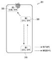
- FIGS. 2A, 2B, and 2C are diagrams illustrating a problem situation that may occur due to reflected waves or IMDs in an electronic device.
- FIG 3 is a diagram illustrating a problem situation due to an IMD in an electronic device.
- 4A and 4B are graphs for describing IMD generation in an electronic device.
- 5A and 5B are circuit diagrams of electronic devices according to various embodiments of the present disclosure.
- FIG. 6 is a circuit diagram of an electronic device according to various embodiments of the present disclosure.
- FIG 7, 8A, 8B, and 8C are diagrams for describing partial structures applicable to an electronic device according to various embodiments of the present disclosure.
- 9, 10, and 11 are flowcharts illustrating a method for improving antenna performance of an electronic device according to various embodiments of the present disclosure.
- 12A and 12B are diagrams illustrating an effect of an electronic device according to various embodiments of the present disclosure.
- the electronic device 101 communicates with the electronic device 102 through the first network 198 (eg, a short-range wireless communication network), or the second network 199 It may communicate with the electronic device 104 or the server 108 through (eg, a remote wireless communication network). According to an embodiment, the electronic device 101 may communicate with the electronic device 104 through the server 108.
- the first network 198 eg, a short-range wireless communication network
- the second network 199 It may communicate with the electronic device 104 or the server 108 through (eg, a remote wireless communication network).
- the electronic device 101 may communicate with the electronic device 104 through the server 108.
- the electronic device 101 includes a processor 120, a memory 130, an input device 150, an audio output device 155, a display device 160, an audio module 170, a sensor module ( 176), interface 177, haptic module 179, camera module 180, power management module 188, battery 189, communication module 190, subscriber identification module 196, or antenna module 197 ).
- the components for example, the display device 160 or the camera module 180
- the sensor module 176 eg, a fingerprint sensor, an iris sensor, or an illuminance sensor
- the display device 160 eg., a display
- the sensor module 176 eg, a fingerprint sensor, an iris sensor, or an illuminance sensor
- the processor 120 executes software (eg, the program 140) to execute at least one other component (eg, hardware or software component) of the electronic device 101 connected to the processor 120. It can be controlled and can perform various data processing or operations. According to one embodiment, as at least part of data processing or computation, the processor 120 may receive instructions or data received from other components (eg, the sensor module 176 or the communication module 190) in the volatile memory 132. Loaded into, process instructions or data stored in volatile memory 132, and store result data in non-volatile memory 134.
- software eg, the program 140
- the processor 120 may receive instructions or data received from other components (eg, the sensor module 176 or the communication module 190) in the volatile memory 132. Loaded into, process instructions or data stored in volatile memory 132, and store result data in non-volatile memory 134.
- the processor 120 includes a main processor 121 (eg, a central processing unit or an application processor), and an auxiliary processor 123 (eg, a graphics processing unit, an image signal processor) that can be operated independently or together. , A sensor hub processor, or a communication processor). Additionally or alternatively, the coprocessor 123 may be set to use lower power than the main processor 121, or to be specialized for a designated function. The coprocessor 123 may be implemented separately from the main processor 121 or as part of it.
- a main processor 121 eg, a central processing unit or an application processor
- an auxiliary processor 123 eg, a graphics processing unit, an image signal processor
- the coprocessor 123 may be set to use lower power than the main processor 121, or to be specialized for a designated function.
- the coprocessor 123 may be implemented separately from the main processor 121 or as part of it.
- the coprocessor 123 may replace, for example, the main processor 121 while the main processor 121 is in an inactive (eg, sleep) state, or the main processor 121 may be active (eg, execute an application) ) With the main processor 121 while in the state, at least one of the components of the electronic device 101 (for example, the display device 160, the sensor module 176, or the communication module 190) It can control at least some of the functions or states associated with.
- the coprocessor 123 eg, image signal processor or communication processor
- may be implemented as part of other functionally relevant components eg, camera module 180 or communication module 190). have.
- the memory 130 may store various data used by at least one component of the electronic device 101 (eg, the processor 120 or the sensor module 176).
- the data may include, for example, software (eg, the program 140) and input data or output data for commands related thereto.
- the memory 130 may include a volatile memory 132 or a non-volatile memory 134.
- the program 140 may be stored as software in the memory 130, and may include, for example, an operating system 142, middleware 144, or an application 146.
- the input device 150 may receive commands or data to be used for components (eg, the processor 120) of the electronic device 101 from outside (eg, a user) of the electronic device 101.
- the input device 150 may include, for example, a microphone, mouse, keyboard, or digital pen (eg, a stylus pen).
- the audio output device 155 may output an audio signal to the outside of the electronic device 101.
- the audio output device 155 may include, for example, a speaker or a receiver.
- the speaker can be used for general purposes such as multimedia playback or recording playback, and the receiver can be used to receive an incoming call.
- the receiver may be implemented separately from, or as part of, a speaker.
- the display device 160 may visually provide information to the outside of the electronic device 101 (eg, a user).
- the display device 160 may include, for example, a display, a hologram device, or a projector and a control circuit for controlling the device.
- the display device 160 may include a touch circuitry configured to sense a touch, or a sensor circuit (eg, a pressure sensor) configured to measure the strength of the force generated by the touch. have.
- the audio module 170 may convert sound into an electrical signal, or vice versa. According to an embodiment, the audio module 170 acquires sound through the input device 150, or an external electronic device (eg, directly or wirelessly connected to the sound output device 155 or the electronic device 101) Sound may be output through the electronic device 102 (eg, speakers or headphones).
- an external electronic device eg, directly or wirelessly connected to the sound output device 155 or the electronic device 101
- Sound may be output through the electronic device 102 (eg, speakers or headphones).
- the sensor module 176 detects an operating state (eg, power or temperature) of the electronic device 101 or an external environmental state (eg, a user state), and generates an electrical signal or data value corresponding to the detected state can do.
- the sensor module 176 includes, for example, a gesture sensor, a gyro sensor, a barometric pressure sensor, a magnetic sensor, an acceleration sensor, a grip sensor, a proximity sensor, a color sensor, an infrared (IR) sensor, a biological sensor, It may include a temperature sensor, a humidity sensor, or an illuminance sensor.
- the interface 177 may support one or more designated protocols that can be used for the electronic device 101 to be directly or wirelessly connected to an external electronic device (eg, the electronic device 102).
- the interface 177 may include, for example, a high definition multimedia interface (HDMI), a universal serial bus (USB) interface, an SD card interface, or an audio interface.
- HDMI high definition multimedia interface
- USB universal serial bus
- SD card interface Secure Digital Card interface
- audio interface audio interface
- connection terminal 178 may include a connector through which the electronic device 101 can be physically connected to an external electronic device (eg, the electronic device 102).
- the connection terminal 178 may include, for example, an HDMI connector, a USB connector, an SD card connector, or an audio connector (eg, a headphone connector).
- the haptic module 179 may convert electrical signals into mechanical stimuli (eg, vibration or movement) or electrical stimuli that the user can perceive through tactile or motor sensations.
- the haptic module 179 may include, for example, a motor, a piezoelectric element, or an electrical stimulation device.
- the camera module 180 may capture still images and videos. According to one embodiment, the camera module 180 may include one or more lenses, image sensors, image signal processors, or flashes.
- the power management module 188 may manage power supplied to the electronic device 101.
- the power management module 388 may be implemented, for example, as at least a part of a power management integrated circuit (PMIC).
- PMIC power management integrated circuit
- the battery 189 may supply power to at least one component of the electronic device 101.
- the battery 189 may include, for example, a non-rechargeable primary cell, a rechargeable secondary cell, or a fuel cell.
- the communication module 190 is a direct (eg, wired) communication channel or a wireless communication channel between the electronic device 101 and an external electronic device (eg, the electronic device 102, the electronic device 104, or the server 108). It can support establishing and performing communication through the established communication channel.
- the communication module 190 operates independently of the processor 120 (eg, an application processor), and may include one or more communication processors supporting direct (eg, wired) communication or wireless communication.
- the communication module 190 is a wireless communication module 192 (eg, a cellular communication module, a short-range wireless communication module, or a global navigation satellite system (GNSS) communication module) or a wired communication module 194 (eg : Local area network (LAN) communication module, or power line communication module.
- a wireless communication module 192 eg, a cellular communication module, a short-range wireless communication module, or a global navigation satellite system (GNSS) communication module
- GNSS global navigation satellite system
- LAN Local area network
- Corresponding communication module among these communication modules includes a first network 198 (for example, a short-range communication network such as Bluetooth, WiFi direct, or infrared data association (IrDA)) or a second network 199 (for example, a cellular network, the Internet, or It may communicate with external electronic devices through a computer network (eg, a telecommunication network such as a LAN or WAN).
- a computer network eg, a telecommunication network such as
- the wireless communication module 192 uses a subscriber information (eg, International Mobile Subscriber Identifier (IMSI)) stored in the subscriber identification module 196 within a communication network such as the first network 198 or the second network 199.
- IMSI International Mobile Subscriber Identifier
- the antenna module 197 may transmit a signal or power to the outside (eg, an external electronic device) or receive it from the outside.
- the antenna module may include a single antenna including a conductor formed on a substrate (eg, a PCB) or a radiator made of a conductive pattern.
- the antenna module 197 may include a plurality of antennas. In this case, at least one antenna suitable for a communication method used in a communication network, such as the first network 198 or the second network 199, is transmitted from the plurality of antennas by, for example, the communication module 190. Can be selected.
- the signal or power may be transmitted or received between the communication module 190 and an external electronic device through the at least one selected antenna.
- other components eg, RFIC
- other than the radiator may be additionally formed as part of the antenna module 197.
- peripheral devices for example, a bus, a general purpose input and output (GPIO), a serial peripheral interface (SPI), or a mobile industry processor interface (MIPI)
- GPIO general purpose input and output
- SPI serial peripheral interface
- MIPI mobile industry processor interface
- commands or data may be transmitted or received between the electronic device 101 and the external electronic device 104 through the server 108 connected to the second network 199.
- Each of the electronic devices 102 and 104 may be the same or a different type of device from the electronic device 101.
- all or some of the operations performed on the electronic device 101 may be performed on one or more external devices of the external electronic devices 102, 104, or 108.
- the electronic device 101 when the electronic device 101 needs to perform a certain function or service automatically or in response to a request from a user or another device, the electronic device 101 instead executes the function or service itself.
- one or more external electronic devices may be requested to perform at least a portion of the function or the service.
- the one or more external electronic devices receiving the request may execute at least a part of the requested function or service, or an additional function or service related to the request, and deliver the result of the execution to the electronic device 101.
- the electronic device 101 may process the result, as it is or additionally, and provide it as at least part of a response to the request.
- cloud computing, distributed computing, or client-server computing technology can be used.
- the electronic device may be various types of devices.
- the electronic device may include, for example, a portable communication device (eg, a smart phone), a computer device, a portable multimedia device, a portable medical device, a camera, a wearable device, or a home appliance device.
- a portable communication device eg, a smart phone
- a computer device e.g., a smart phone
- a portable multimedia device e.g., a portable medical device
- a camera e.g., a portable medical device
- a camera e.g., a portable medical device
- a camera e.g., a portable medical device
- a wearable device e.g., a smart bracelet
- a home appliance device e.g., a home appliance
- any (eg, first) component is referred to as a "coupled” or “connected” to another (eg, second) component, with or without the term “functionally” or “communicatively”
- any of the above components can be connected directly to the other components (eg, by wire), wirelessly, or through a third component.
- module may include a unit implemented in hardware, software, or firmware, and may be used interchangeably with terms such as logic, logic blocks, components, or circuits.
- the module may be an integrally configured component or a minimum unit of the component or a part thereof performing one or more functions.
- the module may be implemented in the form of an application-specific integrated circuit (ASIC).
- ASIC application-specific integrated circuit
- Various embodiments of the present document may include one or more instructions stored in a storage medium (eg, internal memory 136 or external memory 138) readable by a machine (eg, electronic device 101). It may be implemented as software (e.g., program 140) that includes.
- a processor eg, processor 120
- the one or more instructions may include code generated by a compiler or code executable by an interpreter.
- the storage medium readable by the device may be provided in the form of a non-transitory storage medium.
- 'non-transitory' only means that the storage medium is a tangible device, and does not include a signal (eg, electromagnetic wave), and this term is used when data is stored semi-permanently. It does not distinguish between temporary storage cases.
- a method according to various embodiments disclosed in this document may be provided as being included in a computer program product.
- Computer program products are commodities that can be traded between sellers and buyers.
- the computer program product is distributed in the form of a device-readable storage medium (eg compact disc read only memory (CD-ROM)), or through an application store (eg Play Store TM ) or two user devices ( It can be distributed (eg, downloaded or uploaded) directly or online between smartphones).
- a portion of the computer program product may be temporarily stored at least temporarily in a storage medium readable by a device such as a memory of a manufacturer's server, an application store's server, or a relay server, or temporarily generated.
- each component (eg, module or program) of the above-described components may include a singular or a plurality of entities.
- one or more components or operations of the above-described corresponding components may be omitted, or one or more other components or operations may be added.
- a plurality of components eg, modules or programs
- the integrated component may perform one or more functions of each component of the plurality of components the same or similar to that performed by the corresponding component among the plurality of components prior to the integration. .
- operations performed by a module, program, or other component may be executed sequentially, in parallel, repeatedly, or heuristically, or one or more of the operations may be executed in a different order, or omitted Or, one or more other actions can be added.
- the reflected wave may mean that at least a part of the transmission signal Tx is reflected and reversed.
- the electronic device 201 may include an antenna 211, a transmission amplifier 213, a reception amplifier 215, and a transmission / reception circuit 230.
- the transmission signal (Tx) input to the transmission amplifier 213 is not properly output through the antenna 211 and is reflected and reflected, resulting in loss of circuit elements (eg, the transmission amplifier 213) or antenna performance (eg: Sensitivity or transmission performance).
- FIG. 2A 221 illustrates an inflow path of the reflected wave due to the transmission signal Tx.
- a higher output power may be required to the transmit amplifier 213 than the conventional one.
- structural constraints eg, device miniaturization, narrow antenna sector.
- 2B and 2C illustrate interference or IMD problem situations due to the use of multiple antennas or multiple frequency bands.
- the electronic device 201 may include a plurality of antennas 211 and 251 to use various frequency bands. Due to the plurality of antennas 211 and 251 using different frequencies, an interference component between signals or an IMD component of a new frequency may occur. IMD may mean that a plurality of (eg, two or more) frequencies interfere with each other and unnecessary frequency components (parasitic components) appear. For example, an output frequency component combined with a difference and a sum of harmonic frequencies of two different input frequency signals may appear.
- 2B and 2C are examples of a dual connectivity structure supporting a first frequency band (eg, LTE B3 band) and a second frequency band (eg, 5G N77 band).
- a first frequency band eg, LTE B3 band
- a second frequency band eg, 5G N77 band
- a plurality of signals (eg, two or more) having different frequencies may be simultaneously output from one electronic device 201.
- the antenna performance eg, sensitivity, transmission performance, or reception performance
- the antenna performance may be seriously deteriorated due to interference or IMD between a plurality of signals using adjacent frequencies.
- the electronic device 201 may include a first antenna 211, a first transmit amplifier 213, a first receive amplifier 215, and a first transmit / receive circuit 230 as shown in FIGS. 2B and 2C. You can.
- the electronic device 201 may include a second antenna 251, a second transmit amplifier 253, a second receive amplifier 255 and a second transmit / receive circuit 270.
- the first antenna 211, the first transmit amplifier 213, the first receive amplifier 215, and the first transmit / receive circuit 230 are used for the use of the first frequency band (eg, LTE B3 band).
- the second antenna 251, the second transmit amplifier 253, the second receive amplifier 255, and the second transmit / receive circuit 270 may be for use of a second frequency band (eg, 5G N77 band).
- At least a portion of the transmission signal Tx output through the first antenna 211 may be introduced into the second antenna 251.
- an unintended interference signal may be input to the second antenna 251.
- 223 illustrates an inflow path of the interference signal due to the transmission signal Tx.
- the second harmonic component of the transmission signal Tx output from the first antenna 211 is output from the first transmission amplifier 213, and the second reception of the second antenna 251 in a dual connection state It may be introduced into the amplifier 255 and cause damage to circuit elements or deterioration of performance (eg, reception performance).
- a first transmission signal in a first frequency band (eg, a transmission signal of f1 frequency in an LTE B3 band, B3 Tx (f1)) and a second transmission signal of a second frequency band (eg, 5G N77 band)
- a transmission signal of the frequency f2 of N77 Tx (f2) an interference signal or an IMD signal of a new frequency generated by the sum or difference of the two frequencies f1 and f2 may occur.
- the first transmission signal (B3 Tx (f1)) of the first frequency band coming out through the first antenna 211 may be introduced into the second antenna 251 to become an interference signal.
- 225 illustrates the ingress path of the interference signal due to the first transmission signal (eg, B3 Tx (f1)).
- the first transmission signal (eg, B3 Tx (f1)) may be mixed with the second transmission signal (eg, N77 Tx (f2)) to generate an IMD component (eg, IMD (f2-f1)).
- These signals e.g., B3 Tx (f1) or IMD (f2-f1)
- the IMD component (eg, IMD (f2-f1)) is again introduced into the first receive amplifier 215 along with the received signal (eg, B3 Rx (f3)) and additional circuit elements (eg, first receive amplifier 215) ) Can cause burnout or deteriorate antenna performance.
- FIG 3 illustrates a problem situation due to IMD in the electronic device 201.
- the first antenna region 310, the second antenna region 320, and the third antenna region 330 for use of multiple frequency bands may be disposed in the electronic device 201.
- the first antenna region 310 may be for use of a first frequency band (eg, B3 band).
- the second antenna region 320 may be for use of a second frequency band (eg, N77 band).
- the third antenna region 330 may be for use of a third frequency band (eg, WiFi band).
- the first transmission signal output through the first antenna region 310 is a second transmission signal output through the second antenna region 320 (eg, N77 Tx ( f2)) to generate an IMD signal (eg, IMD (f2 + f1)).
- the IMD signal (eg, IMD (f2 + f1)) flows back into the signal reception path of the third antenna region 330 to perform antenna performance (eg, sensitivity or reception performance) in a third frequency band (eg, WiFi band). Deterioration may occur.
- 4A and 4B are graphs for describing IMD generation in the electronic device 201.
- the IMD component between two transmission signals may adversely affect transmission performance.
- IMD components may occur at frequencies of 1 or 2 immediately outside the required bandwidth, which may degrade transmission performance.
- the out-of-band radiation may be for improving transmission performance by lowering a transmission power level without affecting information transmission by radiating radio waves on frequencies of 1 or 2 outside a required frequency bandwidth.
- 4A is a dual access structure using two frequency bands (eg, B71 band and N71 band), the IMD of the out-of-band radiation band 410 when transmitting two frequency signals 431 and 435 in the B71 band and the N71 band Spectra 433 and 437 are shown.
- the out-of-band emission band 410 interference between two signals 431 and 435 or IMD components 433 and 437 may occur.
- Interference or IMD components 433 and 437 may affect the out-of-band radiated power level 423, thereby degrading transmission performance.
- the out-of-band radiated power level 421 when the out-of-band radiated power level 421 is at the -50 dBm level during coexistence of the B21 band and the B29 band, when transmitting two frequency signals 431 and 435 in the B71 band and the N71 band, the two frequencies Due to interference between signals 431 and 435 or IMD components 433 and 437, the out-of-band radiated power level 423 may be set to a higher -36 dBm level. Accordingly, the out-of-band radiated power level 423 may be relatively high, and transmission performance may be deteriorated.
- FIG. 4B shows IMD spectrums 463, 471, and 473 when transmitting two frequency signals 461 and 465 in the B41 band and the N41 band in a dual access structure using two frequency bands (eg, B41 band and N41 band). Indicates.
- the transmission power level 481 may be changed due to the IMD components 471 and 473 between the two transmission signals 461 and 465.
- the first band 451 eg, NS04 spectrum emission band
- the second band 453 spurious emission band
- IMD spectrums 471 and 473 may appear in the third band 455 (E-UTRA spectrum emission band).
- IMD3 In the case of the third IMD component (IMD3), it is very close to the frequency band for transmission and reception, which can cause a fatal problem in antenna performance.
- a method of lowering the power level of the IMD component by forcibly degrading the maximum power performance of the signal by MPR may be considered.
- the intended transmission power level of the original signal is also lowered, so the effect of improving transmission performance may be negligible. Accordingly, a more efficient method of reducing the IMD component and preventing damage to circuit elements and deterioration of antenna performance may be required.
- the electronic device 501 may include all or at least a portion of the electronic device 101 shown in FIG. 1.
- the processor 550 of the electronic device 501 may be the processor of FIG. 1 (eg, the processor 120).
- the antenna 511 or the communication module 540 of the electronic device 501 may include at least a portion of the antenna module (eg, 197) or communication module (eg, the wireless communication module 192) of FIG. 1.
- the electronic device 501 of FIG. 5A may be for preventing a problem situation due to the reflected wave illustrated in FIG. 2A.
- the reflected wave is a miss timing or asynchronous operation of the switching module 535, or a reflection characteristic value of the antenna 511 (eg, voltage standing wave ratio (VSWR), reflection coefficient, reflection It can be caused by a misalignment (mismatch) of at least one of the losses.
- VSWR voltage standing wave ratio
- reflection coefficient reflection coefficient
- reflection It can be caused by a misalignment (mismatch) of at least one of the losses.
- the electronic device 501 may include an antenna 511, a transmission amplifier 521, a transmission / reception circuit 530, a communication module 540, and a processor 550.
- the transmitting / receiving circuit 530 (transmitting or receiving circuit, T / R circuit) may include a circulator 531.
- the transmission / reception circuit 530 may include at least one of a duplexer 533, a switching module 535, or a coupler 537.
- the electronic device 501 may further include a receive amplifier 525.
- the communication module 540 may include, for example, a transmit amplifier 521 or a transceiver connected to the receive amplifier 525.
- the processor 550 may be, for example, the processor (at least one of 120, 121, or 123) illustrated in FIG. 1.
- the antenna 511 may emit electromagnetic waves to transmit a designated signal from the electronic device 501 to the space.
- the antenna 511 may receive a signal in the form of electromagnetic waves from the space to the electronic device 501.
- the transmission amplifier 521 may amplify a transmission signal at a transmission end.
- the transmission amplifier 521 may include a power amplifier that minimizes distortion of an output transmission signal and maintains high efficiency characteristics.
- the transmission amplifier 521 may receive and amplify the transmission signal from the communication module 540 and transmit the amplified transmission signal to the antenna 511 through the transmission / reception circuit 530.
- the transmission / reception circuit 530 may include at least one of a circulator 531, a duplexer 533, a switching module 535, or a coupler 537.
- the transmission amplifier 521 and the duplexer 533 may operate differently according to a frequency band or communication method of a transmission signal.
- the transmit amplifier 521 may include a multi-mode multiband (MMMB) power amplifier.
- the duplexer 533 may include a high band (HB) duplexer, a middle band (MB) duplexer, or a low band (LB) duplexer.
- the transmission amplifier 521 may receive a transmission signal from the communication module 540, amplify the received transmission signal, and transmit it to the duplexer 533.
- the duplexer 533 may branch the transmission signal and the reception signal.
- the duplexer 533 may separate the transmission signal and the reception signal and perform filtering on each of the transmission frequency and the reception frequency.
- the duplexer 533 may pass the transmission signal.
- the duplexer 533 may pass the received signal.
- the duplexer 533 may transmit a transmission signal from the communication module 540 to the antenna 511.
- the duplexer 533 may transmit the received signal from the antenna 511 to the communication module 540.
- the duplexer 533 receives a transmission signal from the transmission amplifier 521 and may transmit the transmission signal to the antenna 511 through a coupler 537.
- the duplexer 533 may receive the received signal from the antenna 511 through the coupler 537 and transmit the received signal to the communication module 540.
- the switching module 535 may be disposed between the coupler 537 and the duplexer 533 to provide a switching function.
- the switching module 535 may provide a switching function to transmit and receive signals of various frequency bands through one antenna 511.
- the switching module 535 may provide a switching function to transmit a transmission signal in the first frequency band through the antenna 511.
- the switching module 535 may provide a switching function to receive the received signal in the second frequency band through the same antenna 511.
- the coupler 537 may be a bidirectional coupler.
- the coupler 537 may be connected between the antenna 511 and the duplexer 533.
- the coupler 537 may receive a transmission signal from the duplexer 533.
- the coupler 537 may receive a received signal from the antenna 511.
- the coupler 537 may separately detect a transmission signal and a reception signal.
- the coupler 537 may branch some of the transmission signals transmitted from the duplexer 533 and transmit them to the communication module 540.
- the coupler 537 distinguishes whether the signal output through the duplexer 533 is a signal radiated through the antenna 511 or a signal reflected without being radiated, so that some of them are fed back to the feedback port of the communication module 540 ( FBRx). Some of the transmission signals may be fed back from the coupler 537 to the communication module 540.
- the signal branched through the coupler 537 may include a forward coupling signal.
- the forward coupling signal may be a signal radiated through the antenna 511.
- the forward coupling signal is a part of the transmission signal, and may have the same frequency and phase as the frequency and phase of the transmission signal.
- the strength of the forward coupling signal may be less than that of the transmission signal.
- the forward coupling signal can be used to calculate reflection characteristic values.
- the coupler 537 may transmit a signal reflected from the antenna 511 to the communication module 540.
- the signal reflected from the antenna 511 may be transmitted from the coupler 537 to the communication module 540.
- the signal branched through the coupler 537 may include a reverse coupling signal.
- the signal reflected without being radiated through the antenna 511 may include a reverse coupling signal.
- the reverse coupling signal may include a signal reflected from the antenna 511.
- the reverse coupling signal may include a signal received through the antenna 511.
- the receive amplifier 525 may be located at the rear end of the antenna 511 to amplify the signal received through the antenna 511 and transmit it to the communication module 540.
- the receive amplifier 525 may include a low noise amplifier designed with low noise to optimize noise performance of the electronic device 501 as a whole.
- the communication module 540 may generate a transmission signal.
- the communication module 540 loads transmission data on a carrier and may transmit a transmission signal including the transmission data and the carrier to the antenna 511 side.
- the transmission signal may be transmitted to the outside of the electronic device 501 through the antenna 511 in the form of electromagnetic waves.
- the transmission data may include data to be transmitted by the electronic device 501 to another electronic device (eg, the electronic device 102 or 104 of FIG. 1) or uplink data to be transmitted to an upper node (eg, a base station).
- another electronic device eg, the electronic device 102 or 104 of FIG. 1
- uplink data to be transmitted to an upper node (eg, a base station).
- the communication module 540 may include an oscillator that generates a carrier wave.
- the communication module 540 may include a modulation circuit that performs a modulation operation of loading transmission data on a carrier wave generated from an oscillator.
- the communication module 540 may include a radio frequency (RF) amplifier that amplifies the modulated carrier to enhance the strength of the transmitted signal.
- RF radio frequency
- the communication module 540 can process the received signal.
- the communication module 540 may receive the received signal including the received data and the carrier wave from the antenna 511 and extract the received data from the received signal.
- the communication module 540 may transmit the extracted received data to the processor 550.
- the received data may include data received by the electronic device 501 from another electronic device (eg, the electronic device 102 or 104 of FIG. 1) or downlink data received from an upper node (eg, a base station).
- another electronic device eg, the electronic device 102 or 104 of FIG. 1
- downlink data received from an upper node (eg, a base station).
- the communication module 540 may include a demodulation circuit that performs a demodulation operation to extract received data from the received signal.
- the RF amplifier may amplify the received signal to facilitate extraction of received data from the received signal.
- the processor 550 may control the communication module 540, the transmit amplifier 521, the receive amplifier 525, the transmit / receive circuit 530 and the antenna 511.
- the processor 550 may perform at least some or all of the functions of the communication module 540.
- the processor 550 may control an operation in which the communication module 540 generates a transmission signal.
- the processor 550 may determine or generate transmission data to be included in the transmission signal, and transmit the transmission data to the communication module 540.
- the processor 550 may determine a communication method.
- the communication module 540 may generate a transmission signal from transmission data according to a communication method determined by the processor 550. For example, if the processor 550 determines transmission data in a voice format, and the communication method determines amplitude modulation (AM), the communication module 540 carriers the transmission data in voice format in an amplitude modulation method. It is possible to generate a transmission signal.
- AM amplitude modulation
- the processor 550 may determine the phase and frequency of the transmitted signal.
- the processor 550 may control the communication module 540 such that the transmission signal has a specific phase and specific frequency.
- the processor 550 may transmit a transmission signal through the antenna 511.
- the processor 550 may transmit or receive a signal through the communication module 540.
- the processor 550 may transmit a transmission signal to the communication module 540.
- the transmission signal output through the communication module 540 may be amplified by passing through the transmission amplifier 521.
- the transmission signal may be transmitted through the duplexer 533 to the coupler 537.
- the duplexer 533 may transmit a high-frequency signal transmitted and received through the antenna 511 as a transmission signal and a reception signal for each communication band.
- the transmission signal passing through the coupler 537 may be transmitted to another electronic device (for example, the electronic device 102 or 104 of FIG. 1) or an upper node through the antenna 511.
- the processor 550 may receive a received signal through the antenna 511.
- the received signal may be transmitted to the duplexer 533 through the coupler 537.
- the received signal transmitted to the duplexer 533 may be transmitted to the processor 550 through the communication module 540.
- the processor 550 may separately detect the forward coupling signal for the transmission signal and the reverse coupling signal reflected by the antenna 511 without being radiated by using the coupler 537.
- a circulator 531 may be disposed between the transmit amplifier 521 and the antenna 511.
- the circulator 531 may be a device having directionality.
- the signal input to each port of the circulator 531 may be transmitted to another adjacent port with the same transmission coefficient and reflection coefficient.
- Each port can be both an input port and an output port for adjacent ports.
- the circulator 531 may normally pass a signal in a first direction (eg, an output direction of a transmission signal, a direction from the transmission amplifier 521 side toward the antenna 511).
- the circulator 531 blocks signals in a second direction (eg, a reverse direction in the first direction, an input direction of a received signal, a direction in which a transmission signal is reflected, and a direction from the antenna 511 side to the transmit amplifier 521). Or you can enter it by another route.
- the circulator 531 is disposed between the transmission amplifier 521 and the antenna 511 so that the signal amplified from the transmission amplifier 521 is transmitted to the antenna 511 side with a small loss.
- the circulator 531 may block a signal so that a signal that is reflected from the antenna 511 and is not returned to the transmission amplifier 521 is not transmitted.
- the circulator 531 may transmit a signal from the antenna 511 side to the communication module 540.
- the signal may be a signal received from the antenna 511.
- the signal may include a reflected signal from the antenna 511.
- the reflected signal may include a signal received through the antenna 511 from the outside.
- the reflected signal may include at least a part of the transmitted signal output from the transmit amplifier 521.
- the reflection signal may include a reverse coupling signal.
- the circulator 531 may have a plurality of ports (for example, three).
- the first port of the circulator 531 may be connected to the output terminal of the transmit amplifier 521.
- the second port may be connected to the input terminal of the duplexer 533 in the transmission / reception circuit 530.
- the third port is connected to a power detection port (PDET) of the communication module 540 to transmit at least a portion of the signal received through the antenna 511.
- PDET power detection port
- the normal transmission signal can be passed through the circulator 531 without loss in the direction of the antenna 511.
- Signals reflected and received from the transceiver circuit 530 (eg, the switching module 535) or the antenna 511 are separated from the transmit amplifier 521 by the circulator 531 (eg, a ground or communication module). It can be delivered to the power sensing port (PDET) of (540).
- An attenuator may be added between the circulator 531 and the power sensing port PDET of the communication module 540 to prevent a relatively large signal from being directly input to the communication module 540.
- the circulator 531 may direct a signal (eg, a reflected signal) received through the antenna 511 directly to the ground.
- a signal eg, a reflected signal
- the reflected signal can be simply removed without a separate algorithm for processing the reflected signal or an additional operation such as control of a circuit element (eg, a switching module 535 or a transmission amplifier 521).
- the circulator 531 may receive a signal (eg, a reflected signal) received through the antenna 511 and transmit the reflected signal to the power sensing port PDET of the communication module 540.
- a signal eg, a reflected signal
- the communication module 540 may be connected to the circulator 531 to check a signal received through the antenna 511 (eg, a power detection signal).
- the signal may include some signals (reflected waves) reflected and returned from the switching module 535 or the antenna 511 among transmission signals output from the transmission amplifier 521.
- the communication module 540 may receive and check the signal through the circulator 531.
- the processor 550 checks the signal (eg, a power detection signal) through the communication module 540 and is based at least in part on a that the identified signal is a signal reflected from the antenna 511 determination that), the frequency characteristics of the antenna 511 can be adjusted. In this case, it is possible to effectively prevent damage to the circuit elements (eg, the transmission amplifier 521) due to reflected waves or deterioration of antenna performance.
- the signal eg, a power detection signal
- the communication module 540 may monitor a signal input from the circulator 531 through the power sensing port PDET.
- the signal may be a power detection signal.
- the communication module 540 may continuously or periodically monitor the power detection signal.
- the communication module 540 may monitor whether a specified event requiring IMD component processing (eg, when the power level of the power detection signal exceeds a threshold) occurs.
- the communication module 540 may check or calculate information about the signal (eg, at least one of analog to digital converting (ADC) information, phase information, and frequency information about the signal size).
- information about the signal eg, at least one of analog to digital converting (ADC) information, phase information, and frequency information about the signal size.
- ADC analog to digital converting
- the processor 550 may receive the signal and confirm or analyze the signal using information about the signal (eg, at least one of frequency, magnitude, and phase of the signal).
- the processor 550 may determine whether the signal is a reflected and reversed signal based on information on the signal (eg, at least one of a frequency, a magnitude, and a phase of the signal). For example, when the phase difference between the signal and the transmission signal output through the transmission amplifier 521 is 180 degrees, the processor 550 may determine that the signal is a reflected wave.
- information on the signal eg, at least one of a frequency, a magnitude, and a phase of the signal. For example, when the phase difference between the signal and the transmission signal output through the transmission amplifier 521 is 180 degrees, the processor 550 may determine that the signal is a reflected wave.
- the processor 550 may determine whether the signal is related to a transmission signal output through the transmission amplifier 521 based on the frequency of the signal. For example, when the first frequency of the signal is substantially the same as the second frequency of the transmission signal, the first frequency and the second frequency are included in a designated band (eg, an adjacent band or an out-of-band emission band). In the case, when the first frequency and the second frequency are in a harmonic relationship, the processor 550 may determine that the signal is related to the transmission signal.
- a designated band eg, an adjacent band or an out-of-band emission band.
- the processor 550 may determine a location (eg, the antenna 511, the switching module 535, or the outside of the electronic device 501) where the signal is reflected based on the signal being related to the transmission signal.
- the processor 550 may determine a location where the signal is reflected based on the phase of the signal. For example, the processor 550 may determine a location where the signal is reflected based on a phase difference between the signal and the transmission signal.
- the processor 550 may adjust the frequency characteristic of the antenna 511 based on the position where the signal is reflected.
- the processor 550 is at least associated with the position to adjust the frequency characteristics of the antenna 511, based on the position where the signal is reflected is a specific circuit element (eg, switching module 535) side A reset may be performed on one circuit element (eg, switching module 535). For example, when the location where the signal is reflected is the switching module 535, the processor 550 may interface with the switching module 535 or a transmission amplifier 521 located in front of it (eg, a mobile industry processor interface (MIPI)). ) To reset the switching module 535 or the transmission amplifier 521.
- MIPI mobile industry processor interface
- the processor 550 is based on the position where the signal is reflected is the antenna 511 side, to adjust the frequency characteristic of the antenna 511, the reflection characteristic value of the antenna 511 (eg, voltage standing wave Ratio, reflection coefficient, or at least one of reflection loss) may be tuned (or corrected).
- the processor 550 may use the tuner circuit of the antenna 511 (not shown, for example, may include an inductor, a variable capacitor, and a tuning switch) to perform tuning so that the reflection characteristic values converge to normal values. .
- the voltage standing wave ratio means a height ratio of a standing wave generated by reflection at the antenna 511 stage, and a value of the voltage standing wave ratio may be out of a normal range due to reflected waves in a specific frequency band.
- the value of the voltage standing wave ratio outside the normal range may be adjusted within the normal value.
- the processor 550 checks the location where the signal is reflected (eg, the antenna 511, the switching module 535, or the outside of the electronic device 501) by using the information on the signal. You can.
- the location where the reflected wave is generated may be related to the use conditions of the electronic device 501 (eg, human contact such as gripping of the antenna 511, access to accessories such as earphones) or operating conditions of the device (eg, a dual connection state).
- the impedance change of the antenna 511 may occur depending on the use condition or the device operation condition.
- the processor 550 may adjust the frequency characteristic of the antenna 511 according to the location where the reflected wave is generated.
- the antenna 511 may be designed to be tunable so that the impedance is always placed in the 50 ohm position under the control of the processor 550.
- the frequency characteristics of the antenna 511 can be adaptively adjusted according to changes in use conditions or device operating conditions.
- the impedance of the antenna 511 is placed at a position of 50 ohms that provides optimum performance, so that degradation of antenna performance due to reflected waves can be prevented.
- the power consumption of the electronic device 501 can be reduced.
- the electronic device 501 of FIG. 5B may be for preventing a problem situation due to an interference signal between multiple antennas illustrated in FIG. 2B.
- the electronic device 501 may include a plurality of antennas 511 and 551 as shown.
- 5B illustrates a case where two antennas 511 and 551 are included for convenience of description, but three or more antennas may be included.
- Each antenna 511, 551 may be connected to at least one of the transmit / receive circuits 530, 570, the transmit amplifiers 521, 561, and the receive amplifiers 525, 565.
- Circulators 531 and 571 may be connected to the output terminals of the respective transmit amplifiers 521 and 561.
- the electronic device 501 includes a first antenna 511, a first transmit amplifier 521, a second antenna 551, a second transmit amplifier 561, and a first circular It may include a rater 531, a communication module 540 and a processor 550.
- the electronic device 501 further includes at least one of a first receive amplifier 525, a first transmit / receive circuit 530, a second receive amplifier 565, a second circulator 571, and a second transmit / receive circuit 570. It can contain.
- the first transmission / reception circuit 530 may include at least one of a first circulator 531, a duplexer 533, a switching module 535, and a coupler 537.
- the second transmission / reception circuit 570 may include at least one of a second circulator 571, a filter 573, a switch 575, and a coupler 577.
- Each circuit element e.g., antennas 511, 551
- transmit amplifiers 521, 561 receive amplifiers 525, 565
- circulators 531, 571 transmit / receive circuits 530, 570
- communication module 540 communication module 540
- each circuit element e.g., antennas 511, 551
- transmit amplifiers 521, 561 receive amplifiers 525, 565
- circulators 531, 571 transmit / receive circuits 530, 570
- communication module 540 Alternatively, since the basic operation or function of the processor 550 has been described with reference to FIG. 5A, redundant description is omitted. Components that use the same name or the same reference numerals can perform the same or similar functions.
- the second transmission / reception circuit 570 is illustrated in a different configuration from the first transmission / reception circuit 530, but is only an example for explanation and is not limited thereto.
- the second transmission / reception circuit 570 may have the same configuration as the first transmission / reception circuit 530.
- the switch 575 of the second transmission / reception circuit 570 may be disposed between the coupler 577 and the filter 573 to provide a switching function.
- the switch may be replaced by a switching module 535 supporting extended or various frequency bands.
- the filter 573 may separate the transmission signal and the reception signal and perform filtering on each of the transmission frequency and the reception frequency.
- the filter 573 may be replaced with a duplexer 533 supporting extended or various frequency bands.
- the first antenna 511 and the second antenna 551 radiate electromagnetic waves to the space and transmit signals from the electronic device 501 to the space through the emitted electromagnetic waves.
- the first antenna 511 and the second antenna 551 transmit signals through electromagnetic waves emitted from other devices (for example, an electronic device (the electronic device 102 or 104 of FIG. 1) or a base station (not shown)) into space. It can be received by the electronic device 501.
- the first antenna 511 and the second antenna 551 may handle the transmission signal as part of the transmitting end.
- the first antenna 511 and the second antenna 551 may handle the received signal as part of the receiving end.
- the transmission signal may include a signal radiated from the electronic device 501 to the space through the first antenna 511 and the second antenna 551.
- the first transmission signal may include a signal radiated through the first antenna 511
- the second transmission signal may include a signal radiated through the second antenna 551, respectively.
- the received signal may include a signal coming from the space to the electronic device 501 through the first antenna 511 and the second antenna 551.
- the first antenna 511 and the second antenna 551 may operate in a dependent manner. Both the first antenna 511 and the second antenna 551 may transmit a signal as a transmitting end or receive a signal as a receiving end. The first antenna 511 and the second antenna 551 may simultaneously transmit or receive signals.
- the first antenna 511 and the second antenna 551 may operate independently.
- the first antenna 511 may transmit a signal as a transmitting end, and the second antenna 551 may receive a signal as a receiving end.
- the first antenna 511 and the second antenna 551 may transmit or receive signals at different timings.
- both the first antenna 511 and the second antenna 551 may be advantageous in terms of improving the performance (eg, transmission performance) of the electronic device 501.
- the present invention is not limited thereto, and only one antenna may be used depending on the design.
- the first antenna 511 transmits a transmission signal (eg, B3 Tx (f1)) or a received signal (eg, B3 Rx (f3)) within a first frequency band (eg, B3 band).
- a transmission signal eg, B3 Tx (f1)
- a received signal eg, B3 Rx (f3)
- the second antenna 551 may be used to transmit a transmission signal (eg, N77 Tx (f2)) within a second frequency band (eg, N77 band) or to receive a received signal (eg, N77 Rx (f4)).
- the first transmission amplifier 521 may amplify a first signal in the first frequency band (eg, B3 Tx (f1)).
- the first signal may be a first transmission signal.
- the second transmit amplifier 561 may amplify a second signal in the second frequency band (eg, N77 Tx (f2)).
- the second signal may be a second transmission signal.
- the first antenna 511 may be connected to the first transmit amplifier 521.
- the second antenna 551 may be connected to the second transmit amplifier 561.
- the first circulator 531 may be disposed between the first transmit amplifier 521 and the first antenna 511.
- the first circulator 531 transmits a normal transmission signal to the first antenna 511 with little loss, and an unintended signal (eg, a signal received from the first antenna 511, a reflected wave, an interference signal, or an IMD) At least one of the components) may flow in a specific port (eg, PDET) direction, thereby preventing burnout of the first transmit amplifier 521.
- the unintended signal flowing from the first antenna 511 to the first transmit amplifier 521 may be blocked through the first circulator 531 to prevent burnout of the first transmit amplifier 521.
- a second circulator 571 may be disposed between the second transmit amplifier 561 and the second antenna 551.
- the inflow of the first signal (eg, B3 Tx (f1)) of the first frequency band, which is the cause of the IMD component can be prevented, thereby deteriorating reception performance Can be prevented.
- the communication module 540 may be connected to the first circulator 531 to check the signal received through the first antenna 511.
- one port of the first circulator 531 is connected to the power sensing port PDET_1 of the communication module 540 to transmit a signal from the first antenna 511 side to the communication module 540.
- the signal may be a signal received through the first antenna 511.
- the signal may include an interference signal.
- the interference signal may be that at least a portion of the second signal, which is a transmission signal from the second antenna 551 side, is introduced into the signal reception path of the first antenna 511 side.
- the processor 550 may transmit the first signal in the first frequency band to the first transmit amplifier 521 and the second signal in the second frequency band to the second transmit amplifier 561.
- the processor 550 may check the signal received through the first antenna 511 using the communication module 540.
- the processor 550 uses the second transmit amplifier 561 or the communication module 540 based on at least a portion of the signal received through the first antenna 511 to include at least a portion of the second signal.
- the characteristics of the second signal radiated through the antenna 551 can be adjusted.
- the first circulator 531 may induce the second signal that is unintentionally entered into the transmission / reception path of the first signal to the ground.
- the first circulator 531 may be connected to the power sensing port PDET_1 of the communication module 540 rather than ground.
- the processor 550 periodically monitors a signal coming into the power detection port PDET_1 of the communication module 540 to check or calculate information about the signal (for example, at least one of a signal size, frequency, or phase). have.
- the communication module 540 may receive the signal from the first circulator 531 through the power sensing port PDET_1.
- the processor 550 may check the signal through the communication module 540. When the signal includes at least a portion of the second signal, the processor 550 may transmit the second signal radiated through the second antenna 551 using the second transmit amplifier 561 or the communication module 540. Characteristics can be adjusted.
- the processor 550 may check or analyze the signal using information about the signal (eg, at least one of a signal size, frequency, and phase).
- the processor 550 may determine whether the signal includes at least a portion of the second signal based on the frequency of the signal. The processor 550 may determine whether the size of the second signal is greater than a specified size based on the signal including at least a portion of the second signal.
- Processor 550 is based on the size of the second signal is greater than the specified size, the second signal is radiated through the second antenna 551 using a second transmit amplifier 561 or communication module 540 The intensity can be reduced.
- Processor 550 is based on the size of the second signal is greater than the specified size, the second signal is radiated through the second antenna 551 using a second transmit amplifier 561 or communication module 540 You can change the phase.
- FIG. 6 is a circuit diagram of an electronic device according to various embodiments of the present disclosure.
- the electronic device 501 may include one or more antennas 511. 6 illustrates circuits for two antennas 511 and 551 for convenience, but the electronic device 501 may include one antenna 511 or three or more antennas, and circuits associated with each antenna 511. .
- the electronic device 501 includes a first antenna 511, a first transmit amplifier 621, a second transmit amplifier 625, a first transmit / receive circuit 630, and a communication module At least one of 540 and processor 550 may be included.
- the first transmission / reception circuit 630 may include at least one of a first coupler 635_1, a second coupler 635_2, and a third coupler 635_3.
- the first transmission / reception circuit 630 may further include a circulator 631.
- the first transceiver circuit 630 may further include a hybrid coupler (633_1, 633_2).
- the first transmission / reception circuit 630 may further include at least one of a switching module 634, a filter 637, or a switch 639.
- the electronic device 501 may further include a second antenna 551, a third transmit amplifier 661, and a second transmit / receive circuit 670.
- the third transmit amplifier 661 may correspond to the second transmit amplifier 561 of FIG. 5B.
- the second transmission / reception circuit 670 may correspond to any one of the transmission / reception circuit 230 or 270 of FIG. 2B, the first transmission / reception circuit 530 or the second transmission / reception circuit 570 of FIG. 5B.
- the circuit connected to the second antenna 551 is a circuit connected to the first antenna 511 (eg, the first transmit amplifier) (621), the second transmission amplifier 625, the transmission and reception circuit 630 may have the same or similar structure.
- each circuit element Since the basic operation or function of each circuit element is the same or similar to that of FIGS. 5A and 5B, overlapping descriptions are omitted.
- the first antenna 511 may be used for signal transmission and reception using a first frequency band.
- the second antenna 551 may be used for signal transmission and reception using a second frequency band.
- the electronic device 501 may include a balanced amplifier structure composed of dual transmit amplifiers 621 and 625.
- the first coupler 635_1 and the second coupler 635_2 may be connected to output terminals of the first transmit amplifier 621 and the second transmit amplifier 625, respectively.
- a third coupler 635_3 may be disposed at the front end of the antenna 511.
- the third coupler 635_3 may correspond to the coupler 537 or 577 of FIG. 5B.
- the first coupler 635_1, the second coupler 635_2, and the third coupler 635_3 may be connected to the communication module 540 through the switching module 634.
- the switching module 634 may perform a switching operation to connect each of the first coupler 635_1, the second coupler 635_2, and the third coupler 635_3 with the communication module 540.
- the first transmit amplifier 621 and the second transmit amplifier 625 may amplify a designated signal.
- the first coupler 635_1 may acquire at least a portion of the first signal amplified through the first transmit amplifier 621.
- the second coupler 635_2 may acquire at least a portion of the second signal amplified through the second transmit amplifier 625.
- the third coupler 635_3 may acquire at least a portion of the generated third signal based at least on the first signal and the second signal.
- the communication module 540 may be connected to the first coupler 635_1, the second coupler 635_2, and the third coupler 635_3.
- the communication module 540 is at least a part of the first signal output from each transmit amplifier 621, 625 through the first coupler 635_1 and the second coupler 635_2 connected to the output terminals of each transmit amplifier 621, 625. Alternatively, at least a part of the second signal may be acquired. The communication module 540 may acquire at least a part of the third signal generated based at least on the first signal and the second signal through the third coupler 635_3 of the antenna 511 end.
- the communication module 540 can include a splitter 545.
- the splitter 545 is a signal that is fed back from at least one of the first coupler 635_1, the second coupler 635_2, or the third coupler 635_3 through the switching module 634 (eg, a first signal, a second signal, or And at least one of the third signals.
- the splitter 545 may branch the received feedback signal into a fundamental signal and an IMD (eg, IMD3) signal and send them through each output port 545_1 and 545_2.
- the processor 550 may receive the original signal and the IMD signal of the feedback signal through the communication module 540 and analyze the two received signals.
- the processor 550 may adjust at least one of the first transmit amplifier 621 or the second transmit amplifier 625 to reduce or cancel the IMD signal based on the analysis result.
- the processor 550 may acquire and confirm at least a portion of the first signal, at least a portion of the second signal, and at least a portion of the third signal through the communication module 540.
- the processor 550 may check the original signal and the IMD signal of each of the first signal, the second signal, or the third signal.
- the processor 550 compares the magnitudes of the IMD signals for the first signal, the second signal, or the third signal, and the first transmit amplifier 621 or the second transmit amplifier ( 625) can be controlled (eg, phase or bias adjustment).
- the processor 550 has a magnitude of an IMD signal for at least a portion of the first signal larger than a specified size, and a magnitude of the IMD signal for at least a portion of the second signal and at least a portion of the third signal is substantially (substantially)
- the first transmit amplifier 621 and the second transmit amplifier 625 can be adjusted based at least on determining the same.
- the processor 550 has a size of an IMD signal for at least a portion of the first signal greater than a specified size, and a size of the IMD signal for at least a portion of the second signal and at least a portion of the third signal Based on determining that is substantially the same, the bias of the first transmit amplifier 621 or the second transmit amplifier 625 may be modified to reduce the magnitude of the IMD signal.
- the processor 550 has a size of an IMD signal for at least a portion of the first signal greater than a specified size, and a size of the IMD signal for at least a portion of the second signal and at least a portion of the third signal Based on determining that is substantially the same, the phase of the first transmit amplifier 621 or the second transmit amplifier 625 may be modified to cancel the IMD signal.
- the first transmit amplifier 621 and the second transmit amplifier 625 may be connected in parallel to form a balanced amplifier structure.
- the outputs of the front end of the first transmit amplifier 621 and the second transmit amplifier 561 may be divided into two and connected to the inputs of the first transmit amplifier 621 and the second transmit amplifier 625.
- the outputs of the first transmit amplifier 621 and the second transmit amplifier 625 may be combined again and connected to a subsequent stage.
- hybrid couplers 633_1 and 633_2 may be used on both sides of the input and output terminals of the first transmit amplifier 621 and the second transmit amplifier 625, respectively.
- the original signals output from the first transmit amplifier 621 and the second transmit amplifier 625 may be combined and transmitted to the antenna 511 without loss of transmission power of the input terminal, and the first transmit amplifier 621 And the IMD components output from the second transmit amplifier 625 may cancel each other.
- the processor 550 detects not only the original signal but also the IMD component from the signal fed back through the third coupler 635_3 in front of the antenna 511 using the splitter 545, so that the first transmit amplifier 621 and the second By utilizing the control of the transmission amplifier 625, the effect of canceling the IMD component of the first transmission amplifier 621 and the second transmission amplifier 625 can be further maximized.
- Couplers 635_1 and 635_2 may be added to the respective transmit amplifiers 621 and 625 to match the phase imbalance of signals output from the dual transmit amplifiers 621 and 625 constituting a balanced amplifier structure. Through this structure, it is possible to individually adjust the phase and signal size of each transmit amplifier 621 and 625.
- the consistency of gain variation and phase deviation between the path of the first transmit amplifier 621 and the path of the second transmit amplifiers 621 and 625 may be important.
- the couplers 635_1 and 635_2 are configured at the output terminals of the respective transmit amplifiers 621 and 625, deviation compensation can be performed for each path of the respective transmit amplifiers 621 and 625.
- the couplers 635_1 and 635_2 are configured at the output terminals of the respective transmit amplifiers 621 and 625, the power or phase deviation of the chains of the respective transmit amplifiers 621 and 625 can be known, so that robustness against load conditions is more robust. ).
- First hybrid couplers 633_1 and 633_2 for branching signal lines input to the first transmit amplifier 621 and the second transmit amplifier 625 at the front ends of the first transmit amplifier 621 and the second transmit amplifier 625. ) Can be connected.
- Second hybrid couplers 633_1 and 633_2 for rejoining signal lines output from the first transmit amplifier 621 and the second transmit amplifier 625 at the rear ends of the first transmit amplifier 621 and the second transmit amplifier 625 ) Can be connected.
- Efficient input / output impedance matching can be achieved in the balanced amplifier structure including the first transmit amplifier 621 and the second transmit amplifier 625 by the first hybrid couplers 633_1 and 633_2 and the second hybrid couplers 633_1 and 633_2. .
- the first antenna 511 may be for radiating a signal (eg, a first transmission signal) in a first frequency band.
- the electronic device 501 may further include a first antenna 511 and a second antenna 551 isolated.
- the second antenna 551 may be for radiating a signal in a second frequency band (eg, a second transmission signal).
- the electronic device 501 may include a circulator 631 connected to the output terminals of the dual transmission amplifiers 621 and 625.
- An unintended signal (eg, at least one of a signal, a reflected wave, an interference signal, or an IMD component received from the antenna 511) flowing from the antenna 511 toward the transmit amplifiers 621 and 625 is connected to the circulator 631. It can be blocked through to prevent the burnout of the transmission amplifier (621, 625).
- the circulator 631 may transmit a power detection signal to the communication module 540 through a designated port (eg, PDET).
- the communication module 540 may detect the occurrence of IMD using a power detection signal.
- the communication module 540 is connected to the circulator 631 to check the signal received through the first antenna 511.
- the processor 550 confirms the signal through the communication module 540, and the signal at least partially generates an IMD signal for a signal in a second frequency band (eg, a second transmission signal on the second antenna 551 side).
- the first transmit amplifier 621 or the second transmit amplifier 625 may be adjusted based at least on what is included.
- the communication module 540 may receive a signal from the first antenna 511 through the power sensing port PDET and transmit it to the processor 550.
- the processor 550 may check the received signal and determine that the IMD signal is generated when the signal exceeds a threshold.
- the processor 550 is a first signal, a second signal, or a third signal fed back from the first coupler 635_1, the second coupler 635_2, or the third coupler 635_3 through the communication module 540. You can confirm by receiving.
- the processor 550 compares the magnitudes of the IMD signals for the first signal, the second signal, or the third signal, and determines the phase or bias of the first transmit amplifier 621 or the second transmit amplifier 625 according to the comparison result. By adjusting, the IMD signal can be canceled or reduced.
- the electronic device 501 may include transmit amplifiers 621 and 625 and phase shifters 711 and 713 preceding each transmit amplifier 621 and 625.
- the first transmit amplifier 621 and the second transmit amplifier 625 may have the same structure.
- Each of the transmission amplifiers 621 and 625 may have a multi-stage structure (eg, a two-stage structure) as illustrated in FIG. 7.
- the first transmit amplifier 621 may include a plurality of amplifiers 621_1 and 621_3.
- the second transmission amplifier 625 may include a plurality of amplifiers 625_1 and 625_3.
- Each transmit amplifier 621 or 625 may include a drive stage amplifier 621_1 or 625_1 and a power stage amplifier 621_3 or 625_3.
- a phase shifter 711 or 713 may be added to the input of each transmit amplifier 621 or 625.
- the signal input to the transmission amplifier may be output by being multi-stage amplified through a plurality of amplifiers (eg, 621_1, 621_3).
- the signal amplified by the power stage amplifier eg, 621_3 which is the last stage among the plurality of amplifiers (eg, 621_1, 621_3) may be transmitted to a corresponding antenna (eg, 511).
- the processor 550 may transmit a control signal (eg, Ctrl1, Ctrl2, or Ctrl3) to control at least one of the phase, gain, or bias of each of the transmit amplifiers 621 and 625.
- a control signal eg, Ctrl1, Ctrl2, or Ctrl3
- the processor 550 detects an IMD occurrence based on at least one of a first signal, a second signal, or a third signal fed back from the first coupler 635_1, the second coupler 635_2, and the third coupler 635_3 can do.
- the processor 550 may have a size of an IMD signal for at least a portion of the first signal greater than a specified size, and a size of the IMD signal for at least a portion of the second signal and at least a portion of the third signal. In substantially the same case, it can be determined that an IMD signal has occurred.
- the processor 550 may adjust the respective transmit amplifiers 621 and 625 to reduce or eliminate the IMD component when an IMD occurs. In one embodiment, the processor 550 may correct the bias of the first transmit amplifier 621 and the second transmit amplifier 625. In other embodiments, the processor 550 may modify the phases of the first transmit amplifier 621 and the second transmit amplifier 625.
- the gain characteristic is dominant in the gain characteristic of the driving stage, and the IMD component and power characteristic may be dominant in the linearity or power characteristic of the power stage.
- the original signal and the IMD signal are identified from a feedback signal (eg, at least one of the first signal, the second signal, and the third signal) to control the bias of the driving stage based on the power level of the original signal.
- a feedback signal eg, at least one of the first signal, the second signal, and the third signal
- the bias of the power stage can be optimized to maximize the effect of canceling the IMD component.
- the phase difference between the respective transmit amplifiers 621 and 625 may be compensated to improve the IMD component cancellation effect.
- 8A and 8B are circuit diagrams showing detailed structures of the transmit amplifiers 621 and 625 according to various embodiments.
- each of the transmission amplifiers 621 and 625 may have a multi-stage structure (eg, a two-stage structure).
- the dual transmit amplifiers 621 and 625 may be connected in parallel to form a balanced amplifier structure.
- Each of the transmission amplifiers 621 and 625 may include driving stage amplifiers 621_1 and 625_1 and power stage amplifiers 621_3 and 625_3.
- Input matching circuits 811 and 821 and output matching circuits 815 and 825 may be added to input / output of each of the transmission amplifiers 621 and 625 constituting a balanced amplifier structure.
- Inter-stage matching circuits 813 and 823 may be added between the driving stage amplifiers 621_1 and 625_1 of the respective transmission amplifiers 621 and 625 and the power stage amplifiers 621_3 and 625_3.
- Hybrid couplers 633_1 and 633_2 may be connected to inputs and outputs of the dual transmission amplifiers 621 and 625, respectively.
- the input and output terminals of each transmit amplifier 621 and 625 may be impedance matched to 50 ohms.
- the input and output terminals of the hybrid couplers 633_1 and 633_2 may be impedance matched to 50 ohms.
- each of the transmission amplifiers 621 and 625 includes the input matching circuits 811 and 821, the intermediate stage matching circuits 813 and 823, and the output matching circuits 815 and 825, due to the passive element area
- the size can be increased.
- a structure in which the input matching circuits 811 and 821 and the output matching circuits 815 and 825 are included in the hybrid couplers 633_1 and 633_2 can be applied.
- input matching circuits 811 and 821 may be included in the hybrid coupler 633_1 through impedance adjustment with the first hybrid coupler 633_1.
- the output matching circuits 815 and 825 may be included in the hybrid coupler 633_2 through impedance adjustment with the second hybrid coupler 633_2.
- the overall size of the balanced amplifier structure can be reduced.
- the input and output impedances of the transmission amplifiers 621 and 625 are arbitrary, without having to match all 50 ohm impedance characteristics for the input and output terminals of the respective transmission amplifiers 621 and 625 and the input and output terminals of each hybrid coupler 633_1 and 633_2.
- the area of the passive element can be greatly reduced.
- parallel capacitors 851 and 853 for shorting the second harmonic component which is one of the main causes of generating the IMD component. I can connect.
- the parallel capacitors 851 and 853 may operate as a shunt circuit that removes the corresponding frequency signal. This allows the reflected IMD component to be further preemptively attenuated by the parallel capacitors 851 and 853 before the IMD component is eliminated with the power combination through the hybrid couplers 633_1 and 633_2.
- 8C illustrates a lumped hybrid coupler structure using a variable resistor or switching capacitor.
- the aforementioned parallel capacitors 851 and 853 may be connected as shunt circuits to the first and fourth ports of the hybrid couplers 633_1 and 633_2, which are connected to the output terminals of the two transmit amplifiers 621 and 621. .
- FIG. 9 is a flowchart illustrating a method for improving antenna performance of an electronic device according to various embodiments of the present disclosure.
- the method of FIG. 9 may be performed, for example, by the electronic device 501 of FIG. 5A or 6.
- the method will be described on the assumption of the operation of the electronic device 501 of FIG. 5A.
- the method of FIG. 9 may be for preventing a problem situation due to reflected waves.
- the problem situation due to the reflected wave may occur, for example, due to miss timing or non-synchronization of the switching module 535, or misalignment of the reflection characteristic value of the antenna 511.
- the processor 550 of the electronic device 501 may acquire a signal received through the antenna 511.
- the signal may be transmitted from the antenna 511 side to the communication module 540 through the circulator 531.
- the signal may be input to the processor 550 through the communication module 540 connected to the circulator 531.
- the signal may be periodically input to the processor 550 through the communication module 540.
- the signal may be a signal reflected from the antenna 511 (reflected wave).
- the circulator 531 may receive the reflected signal and transmit it to the communication module 540.
- the processor 550 may control the communication module 540 to radiate a transmission signal to the antenna 511 side through the transmission amplifier 521. At least a part of the transmission signal transmitted from the transmit amplifier 521 side to the antenna 511 side may be reflected from the antenna 511 side to the transmit amplifier 521 side.
- the communication module 540 may acquire a reflected signal through the circulator 531.
- the processor 550 may acquire the reflected signal through the communication module 540.
- the processor 550 may check or analyze the signal obtained from the circulator 531.
- operation 950 may include operations 953 to 957.
- the processor 550 may transmit the antenna based on the state of the signal input through the circulator 531 (for example, at least one of frequency, amplitude, or phase). It can be confirmed whether the signal (reflected wave) reflected from the 511.
- the processor 550 may proceed to operation 955.
- the processor 550 may determine whether the signal is related to the transmission signal Tx output through the transmission amplifier 521 based on the frequency of the signal. For example, when the frequency of the signal is the same as the frequency of the transmission signal Tx or is included within an adjacent range, when the signal is analyzed as a harmonic of the transmission signal, the signal is said to be related to the transmission signal Tx. Can decide.
- the processor 550 may proceed to operation 957.
- the processor 550 may determine where the signal is reflected (reflected wave generation position or point). In one embodiment, the processor 550 may determine a location where the signal is reflected based on the phase of the signal. For example, based on whether the phase of the signal is somewhat different from the phase of the transmission signal Tx, the location where the signal is reflected is a specific circuit element (eg, switching module 535) side or an antenna ( 511) can determine whether or not.
- a specific circuit element eg, switching module 535) side or an antenna ( 511) can determine whether or not.
- the processor 550 may adjust the frequency characteristic of the antenna 511 based at least on that the signal identified through operation 950 is a signal reflected from the antenna 511.
- the processor 550 may adjust the frequency characteristics of the antenna 511 according to the reflected wave generation location identified through operation 957.
- the processor 550 may include at least one circuit element (eg, switching module 535) associated with the identified location. )) Can be reset.
- the processor 550 may interface with the switching module 535 or a transmission amplifier 521 located in front of it (eg, a mobile industry processor interface (MIPI)). ) To reset the switching module 535 or the transmission amplifier 521.
- MIPI mobile industry processor interface
- the processor 550 may include a tuner circuit (not shown, for example, an inductor, a variable capacitor, and a tuning switch) of the antenna 511.
- a tuner circuit not shown, for example, an inductor, a variable capacitor, and a tuning switch
- the reflection characteristic values of the antenna 511 eg, voltage standing wave ratio, reflection coefficient, reflection loss
- the voltage standing wave ratio refers to a height ratio of a standing wave generated by reflection at the antenna 511 end, and a value of the voltage standing wave ratio in a specific frequency band may be outside a normal range.
- the standing wave is variable, and the value of the standing wave ratio in a frequency band outside the normal range may be adjusted within a normal value.
- FIG. 10 is a flowchart illustrating a method for improving antenna performance of an electronic device according to various embodiments of the present disclosure.
- the method of FIG. 10 may be performed, for example, by the electronic device 501 of FIG. 5B or 6.
- the method of FIG. 10 may be for preventing a problem situation due to the multiple antennas or multiple frequency bands illustrated in FIG. 2B.
- the method is performed in the electronic device 501 of FIG. 5B, and at least a part of the first signal (eg, B3 Tx (f1)) radiated through the first antenna 511 is the second antenna 551
- the method will be described on the assumption that it is introduced to the side and generates an interference component.
- the electronic device 501 may operate in a dual connection state using both the first frequency band (eg, B3 Tx band) and the second frequency band (eg, N77 Tx band).
- the first frequency band eg, B3 Tx band
- the second frequency band eg, N77 Tx band
- the processor 550 the communication module 540 radiates a first signal (eg, B3 Tx (f1)) of the first frequency band to the first antenna 511 through the first transmit amplifier 521 Can be controlled.
- the processor 550 controls the communication module 540 to emit a second signal in the second frequency band (eg, N77 Tx (f2)) to the second antenna 551 through the second transmit amplifier 561. can do.
- the first signal (for example, B3 Tx (f1)) transmitted from the first transmit amplifier 521 side to the first antenna 511 side flows into the second antenna 551 side to become an interference signal. Cases may arise.
- the signal may be input to the power sensing port PDET_2 of the communication module 540 through the second circulator 571.
- the communication module 540 of the electronic device 501 may acquire a signal received through the second antenna 551.
- the processor 550 may acquire the signal through the communication module 540.
- the signal sensed by the second antenna 551 may be at least part of a first signal (eg, B3 Tx (f1)) in the first frequency band.
- the signal may be transmitted through the second circulator 571 disposed between the second transmit amplifier 561 and the second antenna 551.
- the signal may be periodically input to the communication module 540 through the second circulator 571.
- the processor 550 may analyze the acquired signal.
- the processor 550 may perform analysis on the state (eg, at least one of frequency, magnitude, or phase) of the interference signal input through the second circulator 571 connected to the second transmission amplifier 561. have.
- operation 1050 may include operation 1053 and operation 1055.
- the processor 550 may check whether the first signal of the first frequency band (eg, B3 Tx (f1)) is correct. Operation 1053 may be an operation for the processor 550 to determine whether an interference component is generated due to signal inflow between the multiple antennas 511.
- the first signal of the first frequency band eg, B3 Tx (f1)
- the processor 550 may proceed to operation 1055.
- the processor 550 may check whether the signal is large enough to affect reception performance. For example, when the size of the interference signal is larger than a specified size, the processor 550 may determine that the interference signal affects reception performance and proceed to operation 1070.
- the processor 550 is based on at least a portion of the signal identified through operation 1050 includes at least a portion of the first signal (eg, B3 Tx (f1)), the second transmit amplifier 561 or communication module
- the characteristics of the second signal (eg, N77 Tx (f2)) radiated through the second antenna 551 may be adjusted using 540.
- the processor 550 When it is determined that the first component (eg, B3 Tx (f1)) is introduced or an interference component is generated as a result of the check in operation 1050, the processor 550 performs operation 1070 to isolate the multiple antennas 511 ( isolation). Operation 1050 may be to control isolation characteristics of at least one of the multiple antennas 511. Operation 1070 may include at least one of operation 1073 and operation 1075. Depending on the embodiment, operation 1073 and operation 1075 may be selectively performed, or both may be performed.
- the processor 550 may change the phase of the first signal (eg, B3 Tx (f1)) in the first frequency band to increase the isolation effect. For example, the processor 550 may change the phase of the first signal (eg, B3 Tx (f1)) from the current phase to a phase shifted in a direction in which the degree of isolation increases.
- the processor 550 may change the phase of the first signal (eg, B3 Tx (f1)) from the current phase to a phase shifted in a direction in which the degree of isolation increases.
- FIG. 11 is a flowchart illustrating a method for improving antenna performance of an electronic device according to various embodiments of the present disclosure.
- the method of FIG. 11 may be performed, for example, by the electronic device 501 of FIG. 6.
- the method of FIG. 11 may be for preventing a problem situation due to the multiple antennas or multiple frequency bands illustrated in FIG. 2C.
- the communication module 540 includes a first coupler 635_1 connected to the output of the first transmit amplifier 621, a second coupler 635_2 connected to the output of the second transmit amplifier 625, And a third coupler 635_3 at the front end of the antenna 511.
- the communication module 540 of the electronic device 501 may receive signals fed back through the first coupler 635_1, the second coupler 635_2, or the third coupler 635_3.
- the feedback signals may include a first signal obtained from the first coupler 635_1, a second signal obtained from the second coupler 635_2, or a third signal obtained from the third coupler 635_3.
- the processor 550 may acquire at least one feedback signal among the first signal, the second signal, or the third signal through the communication module 540.
- the feedback signal may include a signal of an IMD component.
- the feedback signal may include a signal of an IMD component between transmission signals.
- the feedback signal may include a signal before the antenna 511.
- the feedback signal may include a signal (eg, IMD (f2-f1)) of the IMD component due to the first signal (eg, B3 Tx (f1)).
- the feedback signal includes a first signal radiated through the first antenna 511 (eg, B3 Tx (f1)) and a second signal radiated through the second antenna 551 (eg, N77 Tx ( f2)) between IMD signals (eg, IMD (f2-f1)).
- the processor 550 may check or analyze the original signal and the IMD signal from the feedback signal.
- the processor 550 through the communication module 540, the first, second and third signals from the first coupler 635_1, the second coupler 635_2, and the third coupler 635_3
- the processor 550 through the communication module 540, the first, second and third signals from the first coupler 635_1, the second coupler 635_2, and the third coupler 635_3
- the analysis of the state of the IMD signal eg, at least one of frequency, magnitude, or phase.
- operation 1150 may include operation 1153 and operation 1155.
- the processor 550 may determine whether the size of the IMD signal for the first signal obtained from the first coupler 635_1 is greater than a specified size (eg, a default value).
- a specified size eg, a default value
- the processor 550 may obtain a second signal obtained from the second coupler 635_2 and the third coupler 635_3 and It may be determined whether the magnitudes of the IMD signals for the third signal are substantially equal to each other (eg, whether they are in the same range).
- the processor 550 may proceed to operation 1170 to adjust the first transmit amplifier 621 and the second transmit amplifier 625. .
- the size of the IMD signal for the first signal is smaller than a specified size, a subsequent operation for removing or canceling the IMD component may not be performed.
- the processor 550 proceeds to operation 1173 You can proceed.
- the processor 550 may reduce the size of the IMD signal by lowering the transmit power level by correcting the bias of the first transmit amplifier 521 or the second transmit amplifier 561.
- the processor 550 proceeds to operation 1175. You can.
- the processor 550 may remove the IMD signal by correcting the phase of the first transmit amplifier 621 or the second transmit amplifier 625 to compensate for a phase deviation between the two transmit amplifiers 621 and 625. .
- 12A and 12B are diagrams for describing an effect of another electronic device in various embodiments.
- FIG. 12A and 12B illustrate simulation results of isolation characteristics between two antennas, and show IMD signals for each isolation.
- 12A is a comparison example using a single transmission amplifier for each antenna (eg, FIG. 2B), isolation characteristic simulation results, and FIG. 12B may be an isolation characteristic simulation result between two antennas according to the embodiment (eg, FIG. 6).
- the simulation conditions are as follows. :
- Tx2 -Power level of the second transmission signal (Tx2) measured at the output terminal of the first antenna (e.g., the first antenna 511) side transmit amplifier (e.g., transmit amplifier 521): 20dBm, 20dB for 10dB isolation 10dBm for, 0dBm for 30dB
- the isolation performance when the power level of the transmission signal Tx1 is 30 dBm, the isolation performance must be 40 dB or more to satisfy the IMD performance characteristics (see 1211 and 1215). When the power level of the transmission signal Tx1 is 27dBm, isolation of 30dB may be required (see 1213 and 1217).
- antenna design freedom can be increased by minimizing IMD components.
- an electronic device eg, the electronic device 501 includes a transmit amplifier (eg, a transmit amplifier 521), an antenna (eg, an antenna 511), and is disposed between the transmit amplifier and the antenna.
- a circulator eg, a circulator 531
- a communication module eg, a communication module 540
- the processor may check the signal through the communication module, and adjust the frequency characteristic of the antenna based at least on the signal reflected from the antenna.
- the processor may determine whether the signal is a signal reflected from the antenna based on at least one of the frequency, magnitude, and phase of the signal.
- the processor may determine a location where the signal is reflected based on the phase of the signal, and adjust the frequency characteristic of the antenna based on the location where the signal is reflected.
- the processor determines whether the signal is related to a transmission signal output through the transmission amplifier based on the frequency of the signal, and based on the signal being related to the transmission signal, the signal You can check the reflected position.
- the processor may reset the switching module or the transmission amplifier to adjust the frequency characteristic of the antenna, based on the position where the signal is reflected is on the switching module side connected to the antenna.
- the processor may tune the reflection characteristic value of the antenna to adjust the frequency characteristic of the antenna, based on the location where the signal is reflected is on the antenna side.
- the electronic device includes a first transmission amplifier (eg, a first transmission amplifier 521) and a second frequency band for amplifying a first signal in a first frequency band.
- a second transmit amplifier for amplifying the second signal of (eg, second transmit amplifier 561), a first antenna connected to the first transmit amplifier (eg, first antenna 511), and the second transmit amplifier
- a second antenna eg, second antenna 551) connected to the circulator (eg, circulator 531) disposed between the first transmit amplifier and the first antenna, and connected to the circulator to the second antenna
- It may include a communication module (e.g., communication module 540) and a processor (e.g., processor 550) for checking a signal received through one antenna.
- the processor transmits a signal in the first frequency band to the first transmit amplifier, transmits a signal in the second frequency band to the second transmit amplifier, and receives it through the first antenna using the communication module
- the second antenna by using the second transmit amplifier or the communication module, based on at least a part of checking the signal to be received, and at least partially comprising the second signal received through the first antenna
- the characteristics of the second signal emitted through it may be adjusted.
- the processor may determine whether the signal includes at least a portion of the second signal based on the frequency of the signal, and based on the signal including at least a portion of the second signal, the It can be confirmed whether the size of the second signal is greater than a specified size.
- the processor may have the strength of the second signal radiated through the second antenna using the second transmission amplifier or the communication module, based on the magnitude of the second signal being larger than a specified size. Can be reduced.
- the processor may determine the phase of the second signal radiated through the second antenna using the second transmission amplifier or the communication module, based on the size of the second signal being larger than a specified size. Can be changed.
- the electronic device may further include a second circulator (eg, a second circulator 571) disposed between the second transmit amplifier and the second antenna.
- a second circulator eg, a second circulator 571
- the electronic device includes a first transmit amplifier (eg, a first transmit amplifier 621) and a second transmit amplifier (eg, a second transmit amplifier (a) for amplifying a designated signal. 625)), a first coupler (eg, a first coupler 635_1) for acquiring at least a portion of a first signal amplified through the first transmit amplifier, a second signal amplified through the second transmit amplifier
- a second coupler for acquiring at least a portion (eg, a second coupler 635_2)
- a third coupler for acquiring at least a portion of the third signal generated based at least on the first signal and the second signal
- a processor eg, a processor 550
- a processor eg, a processor 550
- the processor acquires at least a portion of the first signal, at least a portion of the second signal, and at least a portion of the third signal through the communication module, and an IMD signal size for at least a portion of the first signal Is greater than a specified size, and based at least on determining that the magnitudes of the IMD signals for at least a portion of the second signal and at least a portion of the third signal are substantially equal, the first transmit amplifier or the second transmit amplifier Can be adjusted.
- the processor may correct a bias of the first transmit amplifier or the second transmit amplifier when adjusting the first transmit amplifier or the second transmit amplifier.
- the processor may correct a phase of the first transmit amplifier or the second transmit amplifier when adjusting the first transmit amplifier or the second transmit amplifier.
- the electronic device may include a first antenna for radiating a signal in a first frequency band, a circulator disposed between the first transmit amplifier or the second transmit amplifier and the first antenna (for example, a circulator).
- Rater 631) may be further included.
- the electronic device is isolated from the first antenna and further includes a second antenna (eg, the second antenna 551) for emitting a fourth signal in a second frequency band. You can.
- a second antenna eg, the second antenna 551
- the communication module may be connected to the circulator to check a signal received through the first antenna.
- the processor may check the signal through the communication module and adjust the first transmit amplifier or the second transmit amplifier based at least on the signal including at least a portion of the IMD signal for the fourth signal.
- the electronic device may include a first hybrid coupler (eg, a first hybrid coupler 633_1) connected to inputs of the first transmit amplifier and the second transmit amplifier, and the first transmit amplifier and the first A second hybrid coupler (eg, the first hybrid coupler 633_2) connected to the output of the two transmit amplifiers may be further included.
- a first hybrid coupler eg, a first hybrid coupler 633_1
- the first transmit amplifier and the first A second hybrid coupler eg, the first hybrid coupler 633_2 connected to the output of the two transmit amplifiers may be further included.
- the first hybrid coupler may include an input impedance matching circuit (eg, an input matching circuit 811), and the second hybrid coupler may include an output impedance matching circuit (output matching circuit 815).
- the electronic device includes a first parallel capacitor (eg, first parallel capacitor 851) connected to the first coupler, and a second parallel capacitor (eg, second parallel capacitor 853) connected to the second coupler. It may further include.
- the first transmission amplifier and the second transmission amplifier may include driving stage amplifiers (eg, driving stage amplifiers 621_1 and 625_1) and power stage amplifiers 621_3 and 625_3, respectively.
- driving stage amplifiers eg, driving stage amplifiers 621_1 and 625_1
- power stage amplifiers 621_3 and 625_3 respectively.
- the processor adjusts the first transmit amplifier or the second transmit amplifier, a bias of a power stage amplifier of each of the first transmit amplifier and the second transmit amplifier based on an IMD signal for at least a portion of the first signal Can be modified.
Landscapes
- Physics & Mathematics (AREA)
- Electromagnetism (AREA)
- Engineering & Computer Science (AREA)
- Computer Networks & Wireless Communication (AREA)
- Signal Processing (AREA)
- Nonlinear Science (AREA)
- Transceivers (AREA)
Abstract
La présente invention concerne un dispositif électronique pouvant comprendre: un amplificateur d'émission; une antenne; un circulateur disposé entre l'amplificateur d'émission et l'antenne; un module de communication qui est relié au circulateur et qui sert à vérifier un signal reçu par l'intermédiaire de l'antenne; et un processeur. Le processeur peut être réglé pour vérifier le signal par l'intermédiaire du module de communication et adapter les caractéristiques de fréquence de l'antenne en se basant au moins sur le fait que le signal est un signal réfléchi provenant de l'antenne. Divers modes de réalisation sont possibles.
Priority Applications (3)
| Application Number | Priority Date | Filing Date | Title |
|---|---|---|---|
| EP19862781.2A EP3843295A4 (fr) | 2018-09-21 | 2019-09-20 | Dispositif électronique de commande d'un circuit de communication sur la base d'un signal reçu en provenance d'une antenne |
| US17/278,003 US11558128B2 (en) | 2018-09-21 | 2019-09-20 | Electronic device for controlling communication circuit on basis of signal received from antenna |
| CN201980062045.2A CN112753175B (zh) | 2018-09-21 | 2019-09-20 | 用于基于从天线接收的信号来控制通信电路的电子装置 |
Applications Claiming Priority (2)
| Application Number | Priority Date | Filing Date | Title |
|---|---|---|---|
| KR10-2018-0113553 | 2018-09-21 | ||
| KR1020180113553A KR102554666B1 (ko) | 2018-09-21 | 2018-09-21 | 안테나로부터 수신되는 신호에 기반하여 통신 회로를 제어하는 전자 장치 |
Publications (1)
| Publication Number | Publication Date |
|---|---|
| WO2020060306A1 true WO2020060306A1 (fr) | 2020-03-26 |
Family
ID=69887580
Family Applications (1)
| Application Number | Title | Priority Date | Filing Date |
|---|---|---|---|
| PCT/KR2019/012264 Ceased WO2020060306A1 (fr) | 2018-09-21 | 2019-09-20 | Dispositif électronique de commande d'un circuit de communication sur la base d'un signal reçu en provenance d'une antenne |
Country Status (5)
| Country | Link |
|---|---|
| US (1) | US11558128B2 (fr) |
| EP (1) | EP3843295A4 (fr) |
| KR (1) | KR102554666B1 (fr) |
| CN (1) | CN112753175B (fr) |
| WO (1) | WO2020060306A1 (fr) |
Families Citing this family (5)
| Publication number | Priority date | Publication date | Assignee | Title |
|---|---|---|---|---|
| US11476582B2 (en) * | 2020-06-29 | 2022-10-18 | Baker Hughes Oilfield Operations Llc | Tuning systems and methods for downhole antennas |
| WO2023277351A1 (fr) * | 2021-06-28 | 2023-01-05 | 삼성전자주식회사 | Dispositif électronique à conversion ascendante/descendante de fréquence et oscillateur local à faible bruit à ondes millimétriques |
| CN114355388B (zh) * | 2021-12-30 | 2023-04-07 | 浙江时空道宇科技有限公司 | 一种用于低轨卫星导航增强系统的双频发射组件及系统 |
| CN115865125B (zh) * | 2023-03-01 | 2023-06-30 | 成都九洲迪飞科技有限责任公司 | 双通道收发单元 |
| US20250047313A1 (en) * | 2023-08-01 | 2025-02-06 | Samsung Electronics Co., Ltd. | Method and apparatus for load impedance-aware effective isotropic radiated power (eirp) calibration in fr2 phased array transmitters |
Citations (5)
| Publication number | Priority date | Publication date | Assignee | Title |
|---|---|---|---|---|
| US8525648B1 (en) * | 2008-06-25 | 2013-09-03 | Ezero Technologies Llc | Backscatter passive wireless controller with IMD frequency coding |
| KR101559519B1 (ko) * | 2015-05-28 | 2015-10-14 | (주)더원아이앤씨 | 급전선 공유기 및 공유 시스템 |
| KR101722935B1 (ko) * | 2016-07-12 | 2017-04-05 | 주식회사 웨이브트랙 | Pimd 간섭 저감 장치 및 이를 포함하는 이동통신 시스템 |
| WO2017223141A1 (fr) * | 2016-06-22 | 2017-12-28 | Skyworks Solutions, Inc. | Agencements de coupleur électromagnétique pour la détection de puissance multi-fréquence et dispositifs associés |
| KR20180061842A (ko) * | 2016-11-30 | 2018-06-08 | 주식회사 케이엠더블유 | 수동상호변조왜곡 제거 방법 및 이를 이용한 안테나 장치 |
Family Cites Families (17)
| Publication number | Priority date | Publication date | Assignee | Title |
|---|---|---|---|---|
| GB2265269B (en) * | 1992-03-02 | 1995-08-30 | Motorola Ltd | Radio transmitter with linearization training sequence |
| US6111462A (en) | 1998-11-18 | 2000-08-29 | Mucenieks; Lance T. | RF power amplifier linearization using parallel RF power amplifiers having intermod-complementing predistortion paths |
| SE516531C2 (sv) * | 1999-10-29 | 2002-01-29 | Allgon Ab | Antennanordning omkopplingsbar mellan ett flertal konfigurationstillstånd i avhängighet av en mottagen storhet samt därtill hörande metod |
| US8195744B2 (en) | 2004-07-09 | 2012-06-05 | Orb Networks, Inc. | File sharing system for use with a network |
| US9780437B2 (en) * | 2005-06-22 | 2017-10-03 | Michael E. Knox | Antenna feed network for full duplex communication |
| US7696841B2 (en) | 2005-06-23 | 2010-04-13 | Avago Technologies Wireless Ip (Singapore) Pte. Ltd. | Power amplifier utilizing quadrature hybrid for power dividing, combining and impedance matching |
| JP5234768B2 (ja) * | 2008-09-26 | 2013-07-10 | 日本電気株式会社 | ディジタル歪み補償増幅器及びディジタル歪み補償増幅器の出力端子から入力された入力波の制御方法 |
| US8045926B2 (en) * | 2008-10-15 | 2011-10-25 | Nokia Siemens Networks Oy | Multi-transceiver architecture for advanced Tx antenna monitoring and calibration in MIMO and smart antenna communication systems |
| JP2011193191A (ja) * | 2010-03-15 | 2011-09-29 | Renesas Electronics Corp | 半導体集積回路およびそれを内蔵した高周波モジュール |
| US8687529B2 (en) | 2011-07-22 | 2014-04-01 | Symbol Technologies, Inc. | Circulator tuning for reduced intermodulation distortion in a wireless communication device |
| DE102011083066B4 (de) * | 2011-09-20 | 2015-05-07 | Siemens Aktiengesellschaft | Vorrichtung zur Leistungsmessung und Magnetresonanzeinrichtung |
| US10243719B2 (en) * | 2011-11-09 | 2019-03-26 | The Board Of Trustees Of The Leland Stanford Junior University | Self-interference cancellation for MIMO radios |
| JP2013142634A (ja) * | 2012-01-11 | 2013-07-22 | Fujitsu Ltd | Vswr検出回路 |
| US9124355B2 (en) | 2012-08-22 | 2015-09-01 | Google Technology Holdings LLC | Tunable notch filtering in multi-transmit applications |
| US10568015B2 (en) | 2015-08-05 | 2020-02-18 | Lg Electronics Inc. | Method for performing channel access in wireless LAN system and apparatus therefor |
| US10128874B2 (en) * | 2015-08-28 | 2018-11-13 | Qorvo Us, Inc. | Radio frequency coupler circuitry |
| EP3665880B1 (fr) * | 2017-08-10 | 2025-04-30 | Outdoor Wireless Networks LLC | Procédés et appareils pour pré-distorsion numérique |
-
2018
- 2018-09-21 KR KR1020180113553A patent/KR102554666B1/ko active Active
-
2019
- 2019-09-20 WO PCT/KR2019/012264 patent/WO2020060306A1/fr not_active Ceased
- 2019-09-20 US US17/278,003 patent/US11558128B2/en active Active
- 2019-09-20 EP EP19862781.2A patent/EP3843295A4/fr not_active Withdrawn
- 2019-09-20 CN CN201980062045.2A patent/CN112753175B/zh active Active
Patent Citations (5)
| Publication number | Priority date | Publication date | Assignee | Title |
|---|---|---|---|---|
| US8525648B1 (en) * | 2008-06-25 | 2013-09-03 | Ezero Technologies Llc | Backscatter passive wireless controller with IMD frequency coding |
| KR101559519B1 (ko) * | 2015-05-28 | 2015-10-14 | (주)더원아이앤씨 | 급전선 공유기 및 공유 시스템 |
| WO2017223141A1 (fr) * | 2016-06-22 | 2017-12-28 | Skyworks Solutions, Inc. | Agencements de coupleur électromagnétique pour la détection de puissance multi-fréquence et dispositifs associés |
| KR101722935B1 (ko) * | 2016-07-12 | 2017-04-05 | 주식회사 웨이브트랙 | Pimd 간섭 저감 장치 및 이를 포함하는 이동통신 시스템 |
| KR20180061842A (ko) * | 2016-11-30 | 2018-06-08 | 주식회사 케이엠더블유 | 수동상호변조왜곡 제거 방법 및 이를 이용한 안테나 장치 |
Non-Patent Citations (1)
| Title |
|---|
| See also references of EP3843295A4 * |
Also Published As
| Publication number | Publication date |
|---|---|
| US20210359771A1 (en) | 2021-11-18 |
| CN112753175B (zh) | 2023-03-14 |
| KR20200034160A (ko) | 2020-03-31 |
| US11558128B2 (en) | 2023-01-17 |
| CN112753175A (zh) | 2021-05-04 |
| EP3843295A1 (fr) | 2021-06-30 |
| EP3843295A4 (fr) | 2022-02-16 |
| KR102554666B1 (ko) | 2023-07-13 |
Similar Documents
| Publication | Publication Date | Title |
|---|---|---|
| WO2021118228A1 (fr) | Dispositif électronique et procédé de commutation d'antennes associé | |
| WO2020060306A1 (fr) | Dispositif électronique de commande d'un circuit de communication sur la base d'un signal reçu en provenance d'une antenne | |
| WO2021107552A1 (fr) | Procédé et appareil pour fournir une tension à un amplificateur à l'aide de multiples régulateurs linéaires | |
| WO2020122593A1 (fr) | Dispositif électronique servant à atténuer au moins une partie du signal reçu par une antenne et procédé de commande de signal de communication | |
| WO2019050262A1 (fr) | Dispositif électronique comprenant un système de communication sans fil, pour traiter un signal d'émission ou un signal de réception | |
| WO2021006608A1 (fr) | Dispositif électronique de prise en charge de connectivité double et procédé de régulation de puissance associé | |
| WO2021206366A1 (fr) | Dispositif électronique comprenant une antenne et procédé de commande de sortie associée avec une antenne dans un dispositif électronique | |
| WO2022086089A1 (fr) | Dispositif électronique pliable comprenant une antenne | |
| WO2021215714A1 (fr) | Dispositif électronique et procédé de définition, par dispositif électronique, du trajet d'antenne d'un signal de transmission | |
| WO2022045855A1 (fr) | Dispositif électronique et procédé pour régler, par un dispositif électronique, un trajet de signal de transmission | |
| WO2019045547A1 (fr) | Dispositif électronique comprenant une antenne | |
| WO2021172849A1 (fr) | Circuit de connexion double et dispositif électronique le comprenant | |
| WO2020040554A1 (fr) | Procédé de réglage de phase de signal à entrer dans de multiples antennes, et procédé de mise en oeuvre de dispositif électronique | |
| WO2022177275A1 (fr) | Antenne et appareil électronique comprenant celle-ci | |
| WO2020204318A1 (fr) | Dispositif électronique pour compenser une perte de signal inter-fréquence entre un module d'antenne et un circuit intégré inter-fréquence | |
| WO2021133096A1 (fr) | Module d'antenne et dispositif électronique le comprenant | |
| WO2019107899A1 (fr) | Procédé de configuration de puissance dans un système de communication sans fil et appareil associé | |
| WO2019103511A1 (fr) | Dispositif électronique, et procédé de calibrage de dispositif de communication de dispositif électronique | |
| WO2021251680A1 (fr) | Circuit de communication pour amplifier un signal à l'aide de multiples amplificateurs, et dispositif électronique le comprenant | |
| WO2020076092A1 (fr) | Procédé de détection de signal rf et dispositif électronique pour son execution | |
| WO2024019368A1 (fr) | Dispositif électronique de transmission de rapport de mesure et procédé de fonctionnement de dispositif électronique | |
| WO2024005603A1 (fr) | Modem prenant en charge une pré-distorsion numérique, module d'antenne et son procédé de fonctionnement | |
| WO2019066615A1 (fr) | Dispositif électronique et procédé de commande d'antenne d'un dispositif électronique | |
| WO2025226127A1 (fr) | Dispositif électronique de commande de commutation d'antenne et son procédé de fonctionnement | |
| WO2023171885A1 (fr) | Dispositif électronique de commande de transmission sans fil et son procédé de fonctionnement |
Legal Events
| Date | Code | Title | Description |
|---|---|---|---|
| 121 | Ep: the epo has been informed by wipo that ep was designated in this application |
Ref document number: 19862781 Country of ref document: EP Kind code of ref document: A1 |
|
| NENP | Non-entry into the national phase |
Ref country code: DE |
|
| ENP | Entry into the national phase |
Ref document number: 2019862781 Country of ref document: EP Effective date: 20210323 |