WO2020071003A1 - Dispositif source de lumière, dispositif de projection l'utilisant, et dispositif d'excitation de fluorescence - Google Patents
Dispositif source de lumière, dispositif de projection l'utilisant, et dispositif d'excitation de fluorescenceInfo
- Publication number
- WO2020071003A1 WO2020071003A1 PCT/JP2019/032942 JP2019032942W WO2020071003A1 WO 2020071003 A1 WO2020071003 A1 WO 2020071003A1 JP 2019032942 W JP2019032942 W JP 2019032942W WO 2020071003 A1 WO2020071003 A1 WO 2020071003A1
- Authority
- WO
- WIPO (PCT)
- Prior art keywords
- light
- light source
- source device
- lens
- semiconductor laser
- Prior art date
- Legal status (The legal status is an assumption and is not a legal conclusion. Google has not performed a legal analysis and makes no representation as to the accuracy of the status listed.)
- Ceased
Links
Images







Classifications
-
- G—PHYSICS
- G02—OPTICS
- G02B—OPTICAL ELEMENTS, SYSTEMS OR APPARATUS
- G02B27/00—Optical systems or apparatus not provided for by any of the groups G02B1/00 - G02B26/00, G02B30/00
- G02B27/09—Beam shaping, e.g. changing the cross-sectional area, not otherwise provided for
- G02B27/0916—Adapting the beam shape of a semiconductor light source such as a laser diode or an LED, e.g. for efficiently coupling into optical fibers
-
- G—PHYSICS
- G02—OPTICS
- G02B—OPTICAL ELEMENTS, SYSTEMS OR APPARATUS
- G02B19/00—Condensers, e.g. light collectors or similar non-imaging optics
- G02B19/0033—Condensers, e.g. light collectors or similar non-imaging optics characterised by the use
- G02B19/0047—Condensers, e.g. light collectors or similar non-imaging optics characterised by the use for use with a light source
- G02B19/0052—Condensers, e.g. light collectors or similar non-imaging optics characterised by the use for use with a light source the light source comprising a laser diode
-
- F—MECHANICAL ENGINEERING; LIGHTING; HEATING; WEAPONS; BLASTING
- F21—LIGHTING
- F21V—FUNCTIONAL FEATURES OR DETAILS OF LIGHTING DEVICES OR SYSTEMS THEREOF; STRUCTURAL COMBINATIONS OF LIGHTING DEVICES WITH OTHER ARTICLES, NOT OTHERWISE PROVIDED FOR
- F21V9/00—Elements for modifying spectral properties, polarisation or intensity of the light emitted, e.g. filters
- F21V9/30—Elements containing photoluminescent material distinct from or spaced from the light source
-
- G—PHYSICS
- G02—OPTICS
- G02B—OPTICAL ELEMENTS, SYSTEMS OR APPARATUS
- G02B19/00—Condensers, e.g. light collectors or similar non-imaging optics
- G02B19/0004—Condensers, e.g. light collectors or similar non-imaging optics characterised by the optical means employed
- G02B19/0009—Condensers, e.g. light collectors or similar non-imaging optics characterised by the optical means employed having refractive surfaces only
- G02B19/0014—Condensers, e.g. light collectors or similar non-imaging optics characterised by the optical means employed having refractive surfaces only at least one surface having optical power
-
- G—PHYSICS
- G02—OPTICS
- G02B—OPTICAL ELEMENTS, SYSTEMS OR APPARATUS
- G02B26/00—Optical devices or arrangements for the control of light using movable or deformable optical elements
- G02B26/08—Optical devices or arrangements for the control of light using movable or deformable optical elements for controlling the direction of light
- G02B26/10—Scanning systems
-
- G—PHYSICS
- G02—OPTICS
- G02B—OPTICAL ELEMENTS, SYSTEMS OR APPARATUS
- G02B27/00—Optical systems or apparatus not provided for by any of the groups G02B1/00 - G02B26/00, G02B30/00
- G02B27/01—Head-up displays
- G02B27/0101—Head-up displays characterised by optical features
-
- G—PHYSICS
- G02—OPTICS
- G02B—OPTICAL ELEMENTS, SYSTEMS OR APPARATUS
- G02B27/00—Optical systems or apparatus not provided for by any of the groups G02B1/00 - G02B26/00, G02B30/00
- G02B27/09—Beam shaping, e.g. changing the cross-sectional area, not otherwise provided for
- G02B27/0938—Using specific optical elements
- G02B27/095—Refractive optical elements
- G02B27/0955—Lenses
- G02B27/0966—Cylindrical lenses
-
- G—PHYSICS
- G02—OPTICS
- G02B—OPTICAL ELEMENTS, SYSTEMS OR APPARATUS
- G02B3/00—Simple or compound lenses
- G02B3/02—Simple or compound lenses with non-spherical faces
- G02B3/06—Simple or compound lenses with non-spherical faces with cylindrical or toric faces
Definitions
- the present disclosure relates to a light source device that adjusts an aspect ratio of a light beam emitted from a semiconductor laser and then condenses the light at a predetermined light condensing position, a projection device using the same, and a fluorescence excitation device.
- a conventional light source using a semiconductor laser requires a beam shaping optical system for adjusting the aspect ratio of an elliptical light beam and a collimating lens for converting divergent light into parallel light.
- the beam shaping optical system those combining two cylindrical lenses and those using a lens having a toric surface disposed on both surfaces are known. These beam shaping optical systems have been subjected to optical processing for increasing the divergence angle on the slow axis side and decreasing the divergence angle on the fast axis side with respect to the light beam emitted from the semiconductor laser.
- Patent Document 1 and Patent Document 2 are known.
- the light beam diameter on the fast axis side of the light beam is reduced by the optical processing. Then, there is a problem that the spot diameter at the condensing position of the light source device becomes large with the decrease in the light beam diameter.
- a light source device includes a semiconductor laser, a beam shaping lens that adjusts and transmits an aspect ratio of a light beam emitted from the semiconductor laser, and focuses a light beam that has passed through the beam shaping lens at a focus position.
- the beam shaping lens is a cylindrical lens having negative power in the slow axis direction of the incident light beam.
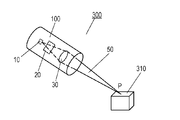
- a projection device includes a light source device and an optical scanning mirror disposed at a condensing position of the light source device.
- the light source device includes a semiconductor laser, a beam shaping lens that adjusts an aspect ratio of a light beam emitted from the semiconductor laser, and a condensing lens that condenses the light beam emitted from the beam shaping lens at a condensing position.
- the beam shaping lens is a cylindrical lens having negative power in the slow axis direction of the incident light beam.
- a fluorescence excitation device includes a light source device and a phosphor disposed at a light condensing position of the light source device.
- the light source device includes a semiconductor laser, a beam shaping lens that adjusts an aspect ratio of a light beam emitted from the semiconductor laser, and a condensing lens that condenses the light beam emitted from the beam shaping lens at a condensing position.
- the beam shaping lens is a cylindrical lens having negative power in the slow axis direction of the incident light beam.
- the present disclosure can reduce the spot diameter at the condensing position.
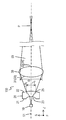
- FIG. 1A is a diagram schematically illustrating a light source device according to the present disclosure when viewed from a slow axis.
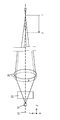
- FIG. 1B is a diagram schematically illustrating a case where the light source device according to the present disclosure is viewed from a fast axis.
- FIG. 2 is a perspective view of a beam shaping lens used in the light source device of the present disclosure.
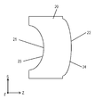
- FIG. 3 is a top view of the beam shaping lens used in the light source device according to the present disclosure as viewed from the positive direction of the fast axis.
- FIG. 4 is a perspective view illustrating an arrangement of a light source and a beam shaping lens used in the light source device of the present disclosure.
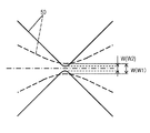
- FIG. 5 is a diagram showing the relationship between the numerical aperture and the spot diameter.
- FIG. 6A is a schematic diagram illustrating a method of adjusting the light-converging position of the light source device according to the present disclosure when viewed from the slow axis.
- FIG. 6B is a schematic diagram illustrating a method of adjusting the light-converging position of the light source device according to the present disclosure when viewed from the fast axis.
- FIG. 7 is a schematic diagram illustrating a projection device according to the present disclosure.
- FIG. 8 is a schematic diagram illustrating the fluorescence excitation device of the present disclosure.
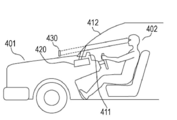
- FIG. 9 is a diagram schematically illustrating an example of an in-vehicle head-up display according to the present disclosure.
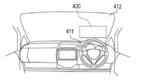
- FIG. 10 is a schematic diagram of the vehicle-mounted head-up display of the present disclosure.
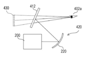
- FIG. 11 is a diagram schematically illustrating a mechanism for displaying an image on the vehicle-mounted head-up display according to the present disclosure.
- FIG. 12A is a top view of the beam shaping lens according to Modification A of the light source device of the present disclosure as viewed from the positive direction of the fast axis.
- FIG. 12B is a top view of the beam shaping lens according to the modified example B of the light source device of the present disclosure as viewed from the positive direction of the fast axis.
- FIG. 12C is a top view of the beam shaping lens according to Modification C of the light source device of the present disclosure, as viewed from the positive direction of the fast axis.
- FIG. 12A is a top view of the beam shaping lens according to Modification A of the light source device of the present disclosure as viewed from the positive direction of the fast axis.
- FIG. 12B is a top view of the beam shaping lens according to the modified example B of the light source device of the present disclosure as viewed from the positive direction of the fast
- FIG. 12D is a top view of the beam shaping lens according to Modification D of the light source device of the present disclosure as viewed from the positive direction of the fast axis.
- FIG. 12E is a top view of the beam shaping lens according to Modification E of the light source device of the present disclosure as viewed from the positive direction of the fast axis.
- each drawing is a schematic diagram and is not necessarily strictly illustrated.
- substantially the same structure is denoted by the same reference numeral, and redundant description is omitted or simplified.
- FIG. 1A and FIG. 1B are diagrams schematically showing a main part configuration of the light source device 100.
- FIG. FIG. 1A is a diagram of the light source device 100 viewed from the direction of the slow axis S.
- FIG. 1B is a diagram of the light source device 100 viewed from the direction of the fast axis F.
- FIG. 2 is a perspective view of the beam shaping lens 20 used in the light source device 100.
- FIG. 3 is a top view of the beam shaping lens 20 shown in FIG. 2 when viewed from the positive direction of the fast axis F.
- FIG. 4 is a perspective view showing an arrangement relationship between the semiconductor laser 10 and the beam shaping lens 20 used in the light source device 100.
- FIG. 5 is a perspective view showing a beam shape of the light beam 50 after passing through the beam shaping lens 20.
- the light source device 100 includes a semiconductor laser 10, a beam shaping lens 20, and a condenser lens 30.
- the cross section of the light beam 50 emitted from the semiconductor laser 10 cut by a plane perpendicular to the optical axis 51 is elliptical as shown in FIG.
- the major axis of the ellipse is the fast axis F of the semiconductor laser 10.
- the fast axis F is parallel to the cleavage plane of the semiconductor laser 10 and coincides with the thickness direction of the active layer 10a of the semiconductor laser 10.
- the minor axis of the ellipse is the slow axis S of the semiconductor laser 10.
- the slow axis S is parallel to the cleavage plane of the semiconductor laser 10 and coincides with the width direction of the active layer 10a of the semiconductor laser 10.
- the beam shaping lens 20 and the condenser lens 30 are arranged on the optical axis 51 of the light beam 50 emitted from the semiconductor laser 10.
- the semiconductor laser 10, the beam shaping lens 20, and the condenser lens 30 are arranged in this order.
- the beam shaping lens 20 has an entrance surface 21 and an exit surface 22.
- the entrance surface 21 is formed by a cylindrical lens having a concave cylindrical surface 23.
- the generatrix of the concave cylindrical surface 23 is parallel to the fast axis F.
- the emission surface 22 has a convex cylindrical surface 24.
- the generatrix of the convex cylindrical surface 24 is parallel to the fast axis F. Therefore, the beam shaping lens 20 has a negative refractive power (power) with respect to the slow axis S of the incident light beam 50 and does not have a refractive power with respect to the fast axis F. That is, the light beam 50 incident on the beam shaping lens 20 has a refractive power only on the side of the slow axis S.
- the negative refractive power refers to an action of expanding the light beam when the light beam passes through the optical element having the negative refractive power.
- An example of an optical element having a negative refractive power is, for example, a concave lens.
- Ray 50 emitted from the beam shaping lens 20 is equal emission angle theta F side of the emission angle theta S and the fast axis F of the side of the slow axis S, and the beam diameter D S of the side of the slow axis S and the fast beam diameter D F of the side in the axial F are equal.
- light rays 50 emitted from the semiconductor laser 10, the beam shaping lens 20, cross section is converted into a beam diameter D F are equal diverging rays of the beam diameter D S and the fast axis F of the slow axis S.
- the cross-sectional shape of the divergent light beam is, for example, a circular shape or a square shape.
- the aspect ratio of the beam diameter D F of the side of the beam diameter D S and the fast axis F of the side of the slow axis S as described above are equal, including variations in the acceptable range in the light source apparatus 100. Allowable range of difference in the beam diameter D F of the side of the beam diameter D S and the fast axis F of the side of the slow axis S is in the range of ⁇ 10% of the beam diameter D S of the side of the slow axis S as a reference.
- the range in which the emission angle ⁇ S on the side of the slow axis S and the emission angle ⁇ F on the side of the fast axis F are equal includes a variation within a range allowed in the light source device 100.
- Tolerance of the difference between the emission angle theta F side of the emission angle theta S and the fast axis F of the side of the slow axis S is in the range of ⁇ 10% the emission angle theta S side of the slow axis S as a reference.
- the condenser lens 30 has an entrance surface 31 and an exit surface 32.
- the entrance surface 31 has a convex lens surface 33 that is rotationally symmetric with respect to the optical axis 51.
- the exit surface 32 has a convex lens surface 34 that is rotationally symmetric with respect to the optical axis 51.
- the incident light beam 50 is condensed at a predetermined light condensing position P on the optical axis 51.
- FIG. 5 shows the light-gathering characteristics according to the numerical aperture (NA).
- NA numerical aperture
- the solid line indicates the light-gathering characteristic of the light beam 50 corresponding to the high NA where the beam diameter D is large.
- W1 in FIG. 5 is the spot diameter of the light beam 50 with a high NA.
- the dashed line indicates the light condensing characteristic of the light beam 50 corresponding to the low NA where the beam diameter D is small.
- W2 in FIG. 5 is the spot diameter of the light beam 50 with a low NA.
- the converging spot W becomes smaller as the beam diameter D incident on the converging lens 30 increases.
- a beam shaping lens 20 is a configuration adjusted to match the beam diameter D S of the side of the slow axis S to the beam diameter D F of the side of the fast axis F.
- This configuration is different from a configuration including adjustment of the beam diameter on the side of the fast axis F (adjustment in the direction of decreasing the emission angle) such as conventional beam shaping, in which the beam diameter of the light beam 50 emitted from the semiconductor laser 10 ( D F ) can be effectively utilized. Therefore, the configuration of the present disclosure can reduce the spot diameter W of the light source device 100.
- FIGS. 6A and 6B are schematic diagrams showing a method of adjusting the light condensing position P of the light source device 100.
- FIG. FIG. 6A is a diagram of the light source device 100 viewed from the direction of the slow axis S.
- FIG. 6B is a diagram of the light source device 100 viewed from the direction of the fast axis F. 6A and 6B, a solid line indicates a state before the position adjustment of the condenser lens 30, and a broken line indicates a state after the position adjustment.
- the condenser lens 30 is brought closer to the semiconductor laser 10 while the positional relationship between the semiconductor laser 10 and the beam shaping lens 20 is maintained. At this time, the light condensing position P also moves to the semiconductor laser 10 side. If this phenomenon is utilized, it is possible to cope with different light condensing positions P by adjusting the position of the light condensing lens 30 in the same light source device 100.
- the focusing position P can be adjusted within a range of 100 mm to 200 mm by adjusting the position of the focusing lens 30.
- Similar adjustment of the light collecting position P can be performed by changing the light collecting characteristics of the light collecting lens 30 without changing the position of the light collecting lens 30.
- the light-collecting characteristics include the focal length and numerical aperture of the light-collecting lens 30. Note that both the position of the condenser lens 30 and the condenser characteristics may be adjusted.
- the distance from the light source to the light condensing position (screen) is freely set when the light scanning device 210 is used as a light source device 100 for a head-up display mounted on a vehicle. Therefore, one light source device 100 can support a wide range of vehicle types.
- FIG. 9 is a diagram schematically showing an in-vehicle head-up display.
- FIG. 10 is a schematic view of the vehicle-mounted head-up display.
- FIG. 11 is a diagram schematically showing a mechanism for displaying an image on the vehicle-mounted head-up display.
- the vehicle-mounted head-up display 420 is mounted on the vehicle 401.
- a virtual image 430 is projected from the in-vehicle head-up display 420 onto the windshield 412, and the person 402 views the projected virtual image 430.
- the virtual image 430 is projected on the display surface of the windshield 412 in FIG.
- the in-vehicle head-up display 420 is mounted on the instrument panel 411.
- the vehicle-mounted head-up display 420 has the projection device 200 and the mirror 220.
- the projection device 200 includes the light source device 100 and the light scanning mirror 210.
- Light emitted from the light transmitting device 200 is projected as a virtual image 430 on the windshield 412 via the mirror 220.
- Virtual image 430 is identified by human eye 402a.
- the distance from the light source device 100 to the windshield 412, which is the light condensing position can be freely set, so that one light source device 100 can support a wide variety of vehicles.
- a YAG phosphor can be used as the phosphor 310.
- a phosphor that emits blue fluorescence such as a BaMgAl 10 O 17 : Eu 2+ (BAM) phosphor or a Sr 3 MgSi 2 O 8 : Eu 2+ (SMS) phosphor, or a green or yellow phosphor (For example, Eu-doped Ca- ⁇ -SiAlON or Eu-doped ⁇ -SiAlON) or a phosphor (for example, Eu-doped CaAlSiN 3 ) that generates red fluorescence.
- the semiconductor laser 10 may be, for example, an AlGaAs / GaAs semiconductor laser having a wavelength of 780 nm, an AlGaInP semiconductor laser having a wavelength of 650 nm, or a GaN semiconductor laser having a wavelength of 420 nm. Further, a semiconductor laser having a wavelength other than those described above, for example, a semiconductor laser that emits ultraviolet light may be used.
- the beam shaping lens 20 and the condensing lens 30 may be formed using optical glass such as BaK4 or optical plastic.
- the beam shaping lens 20 used in the light source device 100 of the present disclosure is not limited to the one shown in the perspective view of FIG. 3 or the top view of FIG. 4, and the following modifications are possible.
- FIGS. 12A to 12E a beam shaping lens 20 according to a modification of the light source device 100 of the present disclosure will be described with reference to FIGS. 12A to 12E.
- FIG. 12A is a top view of the beam shaping lens 20 according to the modified example A of the light source device 100 of the present disclosure, as viewed from the fast axis F direction. That is, the entire exit surface 22 of the beam shaping lens 20 according to Modification A has a convex cylindrical surface shape. As also such a shape, it is possible to have a negative refractive power in the slow axis S direction of the light beam incident to the beam-shaping lens 20, the side of the beam diameter D S of the fast axis F of the side of the slow axis S Can be adjusted so as to match the beam diameter DF .
- FIG. 12B is a top view of the beam shaping lens 20 according to the modified example B of the light source device 100 of the present disclosure as viewed from the direction of the fast axis F. That is, the entire exit surface 22 of the beam shaping lens 20 according to the modification B has a planar shape. As also such a shape, it is possible to have a negative refractive power in the slow axis S direction of the light beam incident to the beam-shaping lens 20, the side of the beam diameter D S of the fast axis F of the side of the slow axis S Can be adjusted so as to match the beam diameter DF .
- FIG. 12C is a top view of the beam shaping lens 20 according to the modification example C of the light source device 100 of the present disclosure as viewed from the direction of the fast axis F. That is, the exit surface 22 of the beam shaping lens 20 according to the modification C has a concave cylindrical surface shape except for the end portions. As also such a shape, it is possible to have a negative refractive power in the slow axis S direction of the light beam incident to the beam-shaping lens 20, the side of the beam diameter D S of the fast axis F of the side of the slow axis S Can be adjusted so as to match the beam diameter DF .
- FIG. 12D is a top view of the beam shaping lens 20 according to the modified example D of the light source device 100 of the present disclosure as viewed from the direction of the fast axis F. That is, the entire exit surface 22 of the beam shaping lens 20 according to the modification D has a concave cylindrical surface shape. As also such a shape, it is possible to have a negative refractive power in the direction of the slow axis S of the light beam incident to the beam-shaping lens 20, on the side of the slow axis S of the beam diameter D S of the fast axis F It can be adjusted to match the beam diameter DF on the side.
- FIG. 12E is a top view of the beam shaping lens 20 according to the modified example E of the light source device 100 of the present disclosure as viewed from the direction of the fast axis F. That is, the entire incident surface 21 of the beam shaping lens 20 according to the modification E has a planar shape. As also such a shape, it is possible to have a negative refractive power in the slow axis S direction of the light beam incident to the beam-shaping lens 20, the side of the beam diameter D S of the fast axis F of the side of the slow axis S Can be adjusted so as to match the beam diameter DF .
- the present disclosure has an effect that the spot diameter of the light source device can be reduced, and is particularly effective for small-sized scanning optical systems.
Landscapes
- Physics & Mathematics (AREA)
- General Physics & Mathematics (AREA)
- Optics & Photonics (AREA)
- Spectroscopy & Molecular Physics (AREA)
- Engineering & Computer Science (AREA)
- General Engineering & Computer Science (AREA)
- Semiconductor Lasers (AREA)
- Projection Apparatus (AREA)
- Optical Filters (AREA)
Abstract
L'invention concerne un dispositif source de lumière, un dispositif de projection l'utilisant et un dispositif d'excitation de fluorescence, dans lesquels un faisceau de lumière émis à partir d'un laser à semiconducteur est condensé au niveau d'un emplacement de condensation prescrit après que le rapport d'aspect dudit faisceau de lumière ait été ajusté, et le diamètre du point lumineux au niveau de l'emplacement de condensation est réduit. Un dispositif source de lumière (100) comprend un laser à semiconducteur (10), une lentille de mise en forme de faisceau (20) qui ajuste le rapport d'aspect d'un faisceau de lumière (50) émis par le laser à semiconducteur (10) et une lentille de condenseur (30) qui condense le faisceau de lumière (50) émis par la lentille de mise en forme de faisceau (20) à un emplacement de condensation (P), la lentille de mise en forme de faisceau (20) étant une lentille cylindrique ayant une puissance négative par rapport à la direction de l'axe lent (S) du faisceau de lumière incidente (50).
Priority Applications (3)
| Application Number | Priority Date | Filing Date | Title |
|---|---|---|---|
| US17/267,340 US20210231964A1 (en) | 2018-10-05 | 2019-08-23 | Light source device, projection device using same, and fluorescence excitation device |
| CN201980059845.9A CN112740096A (zh) | 2018-10-05 | 2019-08-23 | 光源装置及使用其的投影装置、以及荧光激励装置 |
| JP2020550017A JPWO2020071003A1 (ja) | 2018-10-05 | 2019-08-23 | 光源装置、およびそれを用いた投影装置、ならびに蛍光励起装置 |
Applications Claiming Priority (2)
| Application Number | Priority Date | Filing Date | Title |
|---|---|---|---|
| JP2018-189666 | 2018-10-05 | ||
| JP2018189666 | 2018-10-05 |
Publications (1)
| Publication Number | Publication Date |
|---|---|
| WO2020071003A1 true WO2020071003A1 (fr) | 2020-04-09 |
Family
ID=70055765
Family Applications (1)
| Application Number | Title | Priority Date | Filing Date |
|---|---|---|---|
| PCT/JP2019/032942 Ceased WO2020071003A1 (fr) | 2018-10-05 | 2019-08-23 | Dispositif source de lumière, dispositif de projection l'utilisant, et dispositif d'excitation de fluorescence |
Country Status (4)
| Country | Link |
|---|---|
| US (1) | US20210231964A1 (fr) |
| JP (1) | JPWO2020071003A1 (fr) |
| CN (1) | CN112740096A (fr) |
| WO (1) | WO2020071003A1 (fr) |
Citations (5)
| Publication number | Priority date | Publication date | Assignee | Title |
|---|---|---|---|---|
| JPH055853A (ja) * | 1991-06-27 | 1993-01-14 | Ricoh Co Ltd | 光走査光学系および光走査装置 |
| JP2009192789A (ja) * | 2008-02-14 | 2009-08-27 | Mitsubishi Electric Corp | 照明光学系および画像表示装置 |
| US20120257387A1 (en) * | 2011-04-07 | 2012-10-11 | Coherent, Inc. | Diode-laser illuminator with interchangeable modules for changing irradiance and beam dimensions |
| JP2013130835A (ja) * | 2011-12-22 | 2013-07-04 | Sharp Corp | ホモジナイザ、ホモジナイザ装置および照明装置 |
| WO2017138298A1 (fr) * | 2016-02-09 | 2017-08-17 | 三菱電機株式会社 | Dispositif de mise en forme de faisceau et oscillateur laser |
Family Cites Families (7)
| Publication number | Priority date | Publication date | Assignee | Title |
|---|---|---|---|---|
| US6768593B1 (en) * | 2003-06-24 | 2004-07-27 | Suganda Jutamulia | Fiber-coupled laser diode having high coupling-efficiency and low feedback-noise |
| US7287862B2 (en) * | 2005-02-18 | 2007-10-30 | Symbol Technologies, Inc. | Compact image projection module |
| CN101834402B (zh) * | 2009-09-24 | 2012-06-27 | 西安炬光科技有限公司 | 一种半导体激光器侧泵模块 |
| US9323063B2 (en) * | 2011-04-29 | 2016-04-26 | Dhpc Technologies, Inc. | Free-space combining of laser beam radiation |
| JP5589007B2 (ja) * | 2012-01-18 | 2014-09-10 | シャープ株式会社 | 発光装置、照明装置および車両用前照灯 |
| CN107062023A (zh) * | 2017-06-09 | 2017-08-18 | 超视界激光科技(苏州)有限公司 | 一种自适应激光照明灯 |
| DE102018212551B4 (de) * | 2018-07-27 | 2020-06-18 | Q.ant GmbH | Laserlichtquelle und Laser-Projektor damit |
-
2019
- 2019-08-23 WO PCT/JP2019/032942 patent/WO2020071003A1/fr not_active Ceased
- 2019-08-23 CN CN201980059845.9A patent/CN112740096A/zh active Pending
- 2019-08-23 US US17/267,340 patent/US20210231964A1/en not_active Abandoned
- 2019-08-23 JP JP2020550017A patent/JPWO2020071003A1/ja active Pending
Patent Citations (5)
| Publication number | Priority date | Publication date | Assignee | Title |
|---|---|---|---|---|
| JPH055853A (ja) * | 1991-06-27 | 1993-01-14 | Ricoh Co Ltd | 光走査光学系および光走査装置 |
| JP2009192789A (ja) * | 2008-02-14 | 2009-08-27 | Mitsubishi Electric Corp | 照明光学系および画像表示装置 |
| US20120257387A1 (en) * | 2011-04-07 | 2012-10-11 | Coherent, Inc. | Diode-laser illuminator with interchangeable modules for changing irradiance and beam dimensions |
| JP2013130835A (ja) * | 2011-12-22 | 2013-07-04 | Sharp Corp | ホモジナイザ、ホモジナイザ装置および照明装置 |
| WO2017138298A1 (fr) * | 2016-02-09 | 2017-08-17 | 三菱電機株式会社 | Dispositif de mise en forme de faisceau et oscillateur laser |
Also Published As
| Publication number | Publication date |
|---|---|
| US20210231964A1 (en) | 2021-07-29 |
| CN112740096A (zh) | 2021-04-30 |
| JPWO2020071003A1 (ja) | 2021-09-24 |
Similar Documents
| Publication | Publication Date | Title |
|---|---|---|
| US9431795B2 (en) | Laser beam-combining optical device | |
| US8585208B2 (en) | Light source device and projector | |
| JP6525856B2 (ja) | 光源光学系およびこれを用いた投射型表示装置 | |
| CN110160001B (zh) | 照明装置以及车辆用灯具 | |
| US12007557B2 (en) | Optical system | |
| JP2018120111A (ja) | 照明装置及びプロジェクター | |
| JPWO2018051450A1 (ja) | レーザ装置 | |
| CN113759648A (zh) | 照明装置和投影仪 | |
| US20170242266A1 (en) | Illumination device and projector | |
| WO2020071003A1 (fr) | Dispositif source de lumière, dispositif de projection l'utilisant, et dispositif d'excitation de fluorescence | |
| US9851631B2 (en) | Light source optical system and projection display apparatus employing the same | |
| US20180266641A1 (en) | Light device with movable scanning means and optical fiber | |
| JP6790170B2 (ja) | 光源光学系およびこれを用いた投射型表示装置 | |
| JP2015145975A (ja) | 光源装置およびこれを用いた投射型表示装置 | |
| US12352940B2 (en) | Optical system | |
| US20090323176A1 (en) | Single wavelength ultraviolet laser device | |
| US12189103B2 (en) | Optical system | |
| US20100053739A1 (en) | Laser device providing an adjusted field distribution for laser beams thereof | |
| US12483001B2 (en) | Lighting optical system | |
| US12572005B2 (en) | Optical scanning device and image forming device | |
| JP2007185707A (ja) | 光溶着用光学ユニットおよび光溶着装置 | |
| JP6636062B2 (ja) | レーザ合成光学装置 | |
| JP2017054883A (ja) | 光学素子、光学装置、および投影装置 | |
| JPH1068905A (ja) | 半導体レーザの発光パターン補正方法、補正用光学系及び固体レーザ装置 | |
| JPH02190816A (ja) | 線状結像用レンズ |
Legal Events
| Date | Code | Title | Description |
|---|---|---|---|
| 121 | Ep: the epo has been informed by wipo that ep was designated in this application |
Ref document number: 19868512 Country of ref document: EP Kind code of ref document: A1 |
|
| ENP | Entry into the national phase |
Ref document number: 2020550017 Country of ref document: JP Kind code of ref document: A |
|
| NENP | Non-entry into the national phase |
Ref country code: DE |
|
| 122 | Ep: pct application non-entry in european phase |
Ref document number: 19868512 Country of ref document: EP Kind code of ref document: A1 |