WO2020084845A1 - Dispositif d'affichage à cristaux liquides - Google Patents
Dispositif d'affichage à cristaux liquides Download PDFInfo
- Publication number
- WO2020084845A1 WO2020084845A1 PCT/JP2019/027791 JP2019027791W WO2020084845A1 WO 2020084845 A1 WO2020084845 A1 WO 2020084845A1 JP 2019027791 W JP2019027791 W JP 2019027791W WO 2020084845 A1 WO2020084845 A1 WO 2020084845A1
- Authority
- WO
- WIPO (PCT)
- Prior art keywords
- liquid crystal
- crystal display
- wave plate
- display device
- quarter
- Prior art date
- Legal status (The legal status is an assumption and is not a legal conclusion. Google has not performed a legal analysis and makes no representation as to the accuracy of the status listed.)
- Ceased
Links
Images

Classifications
-
- G—PHYSICS
- G02—OPTICS
- G02F—OPTICAL DEVICES OR ARRANGEMENTS FOR THE CONTROL OF LIGHT BY MODIFICATION OF THE OPTICAL PROPERTIES OF THE MEDIA OF THE ELEMENTS INVOLVED THEREIN; NON-LINEAR OPTICS; FREQUENCY-CHANGING OF LIGHT; OPTICAL LOGIC ELEMENTS; OPTICAL ANALOGUE/DIGITAL CONVERTERS
- G02F1/00—Devices or arrangements for the control of the intensity, colour, phase, polarisation or direction of light arriving from an independent light source, e.g. switching, gating or modulating; Non-linear optics
- G02F1/01—Devices or arrangements for the control of the intensity, colour, phase, polarisation or direction of light arriving from an independent light source, e.g. switching, gating or modulating; Non-linear optics for the control of the intensity, phase, polarisation or colour
- G02F1/13—Devices or arrangements for the control of the intensity, colour, phase, polarisation or direction of light arriving from an independent light source, e.g. switching, gating or modulating; Non-linear optics for the control of the intensity, phase, polarisation or colour based on liquid crystals, e.g. single liquid crystal display cells
- G02F1/133—Constructional arrangements; Operation of liquid crystal cells; Circuit arrangements
- G02F1/1333—Constructional arrangements; Manufacturing methods
- G02F1/1335—Structural association of cells with optical devices, e.g. polarisers or reflectors
- G02F1/133553—Reflecting elements
- G02F1/133555—Transflectors
-
- G—PHYSICS
- G02—OPTICS
- G02F—OPTICAL DEVICES OR ARRANGEMENTS FOR THE CONTROL OF LIGHT BY MODIFICATION OF THE OPTICAL PROPERTIES OF THE MEDIA OF THE ELEMENTS INVOLVED THEREIN; NON-LINEAR OPTICS; FREQUENCY-CHANGING OF LIGHT; OPTICAL LOGIC ELEMENTS; OPTICAL ANALOGUE/DIGITAL CONVERTERS
- G02F1/00—Devices or arrangements for the control of the intensity, colour, phase, polarisation or direction of light arriving from an independent light source, e.g. switching, gating or modulating; Non-linear optics
- G02F1/01—Devices or arrangements for the control of the intensity, colour, phase, polarisation or direction of light arriving from an independent light source, e.g. switching, gating or modulating; Non-linear optics for the control of the intensity, phase, polarisation or colour
- G02F1/13—Devices or arrangements for the control of the intensity, colour, phase, polarisation or direction of light arriving from an independent light source, e.g. switching, gating or modulating; Non-linear optics for the control of the intensity, phase, polarisation or colour based on liquid crystals, e.g. single liquid crystal display cells
- G02F1/133—Constructional arrangements; Operation of liquid crystal cells; Circuit arrangements
- G02F1/1333—Constructional arrangements; Manufacturing methods
- G02F1/1335—Structural association of cells with optical devices, e.g. polarisers or reflectors
- G02F1/13363—Birefringent elements, e.g. for optical compensation
- G02F1/133638—Waveplates, i.e. plates with a retardation value of lambda/n
-
- G—PHYSICS
- G02—OPTICS
- G02F—OPTICAL DEVICES OR ARRANGEMENTS FOR THE CONTROL OF LIGHT BY MODIFICATION OF THE OPTICAL PROPERTIES OF THE MEDIA OF THE ELEMENTS INVOLVED THEREIN; NON-LINEAR OPTICS; FREQUENCY-CHANGING OF LIGHT; OPTICAL LOGIC ELEMENTS; OPTICAL ANALOGUE/DIGITAL CONVERTERS
- G02F1/00—Devices or arrangements for the control of the intensity, colour, phase, polarisation or direction of light arriving from an independent light source, e.g. switching, gating or modulating; Non-linear optics
- G02F1/01—Devices or arrangements for the control of the intensity, colour, phase, polarisation or direction of light arriving from an independent light source, e.g. switching, gating or modulating; Non-linear optics for the control of the intensity, phase, polarisation or colour
- G02F1/13—Devices or arrangements for the control of the intensity, colour, phase, polarisation or direction of light arriving from an independent light source, e.g. switching, gating or modulating; Non-linear optics for the control of the intensity, phase, polarisation or colour based on liquid crystals, e.g. single liquid crystal display cells
- G02F1/133—Constructional arrangements; Operation of liquid crystal cells; Circuit arrangements
- G02F1/1333—Constructional arrangements; Manufacturing methods
- G02F1/1335—Structural association of cells with optical devices, e.g. polarisers or reflectors
- G02F1/133528—Polarisers
-
- G—PHYSICS
- G02—OPTICS
- G02F—OPTICAL DEVICES OR ARRANGEMENTS FOR THE CONTROL OF LIGHT BY MODIFICATION OF THE OPTICAL PROPERTIES OF THE MEDIA OF THE ELEMENTS INVOLVED THEREIN; NON-LINEAR OPTICS; FREQUENCY-CHANGING OF LIGHT; OPTICAL LOGIC ELEMENTS; OPTICAL ANALOGUE/DIGITAL CONVERTERS
- G02F1/00—Devices or arrangements for the control of the intensity, colour, phase, polarisation or direction of light arriving from an independent light source, e.g. switching, gating or modulating; Non-linear optics
- G02F1/01—Devices or arrangements for the control of the intensity, colour, phase, polarisation or direction of light arriving from an independent light source, e.g. switching, gating or modulating; Non-linear optics for the control of the intensity, phase, polarisation or colour
- G02F1/13—Devices or arrangements for the control of the intensity, colour, phase, polarisation or direction of light arriving from an independent light source, e.g. switching, gating or modulating; Non-linear optics for the control of the intensity, phase, polarisation or colour based on liquid crystals, e.g. single liquid crystal display cells
- G02F1/133—Constructional arrangements; Operation of liquid crystal cells; Circuit arrangements
- G02F1/1333—Constructional arrangements; Manufacturing methods
- G02F1/1335—Structural association of cells with optical devices, e.g. polarisers or reflectors
- G02F1/13356—Structural association of cells with optical devices, e.g. polarisers or reflectors characterised by the placement of the optical elements
- G02F1/133562—Structural association of cells with optical devices, e.g. polarisers or reflectors characterised by the placement of the optical elements on the viewer side
-
- G—PHYSICS
- G02—OPTICS
- G02F—OPTICAL DEVICES OR ARRANGEMENTS FOR THE CONTROL OF LIGHT BY MODIFICATION OF THE OPTICAL PROPERTIES OF THE MEDIA OF THE ELEMENTS INVOLVED THEREIN; NON-LINEAR OPTICS; FREQUENCY-CHANGING OF LIGHT; OPTICAL LOGIC ELEMENTS; OPTICAL ANALOGUE/DIGITAL CONVERTERS
- G02F1/00—Devices or arrangements for the control of the intensity, colour, phase, polarisation or direction of light arriving from an independent light source, e.g. switching, gating or modulating; Non-linear optics
- G02F1/01—Devices or arrangements for the control of the intensity, colour, phase, polarisation or direction of light arriving from an independent light source, e.g. switching, gating or modulating; Non-linear optics for the control of the intensity, phase, polarisation or colour
- G02F1/13—Devices or arrangements for the control of the intensity, colour, phase, polarisation or direction of light arriving from an independent light source, e.g. switching, gating or modulating; Non-linear optics for the control of the intensity, phase, polarisation or colour based on liquid crystals, e.g. single liquid crystal display cells
- G02F1/133—Constructional arrangements; Operation of liquid crystal cells; Circuit arrangements
- G02F1/1333—Constructional arrangements; Manufacturing methods
- G02F1/1335—Structural association of cells with optical devices, e.g. polarisers or reflectors
- G02F1/13363—Birefringent elements, e.g. for optical compensation
-
- G—PHYSICS
- G02—OPTICS
- G02F—OPTICAL DEVICES OR ARRANGEMENTS FOR THE CONTROL OF LIGHT BY MODIFICATION OF THE OPTICAL PROPERTIES OF THE MEDIA OF THE ELEMENTS INVOLVED THEREIN; NON-LINEAR OPTICS; FREQUENCY-CHANGING OF LIGHT; OPTICAL LOGIC ELEMENTS; OPTICAL ANALOGUE/DIGITAL CONVERTERS
- G02F1/00—Devices or arrangements for the control of the intensity, colour, phase, polarisation or direction of light arriving from an independent light source, e.g. switching, gating or modulating; Non-linear optics
- G02F1/01—Devices or arrangements for the control of the intensity, colour, phase, polarisation or direction of light arriving from an independent light source, e.g. switching, gating or modulating; Non-linear optics for the control of the intensity, phase, polarisation or colour
- G02F1/13—Devices or arrangements for the control of the intensity, colour, phase, polarisation or direction of light arriving from an independent light source, e.g. switching, gating or modulating; Non-linear optics for the control of the intensity, phase, polarisation or colour based on liquid crystals, e.g. single liquid crystal display cells
- G02F1/137—Devices or arrangements for the control of the intensity, colour, phase, polarisation or direction of light arriving from an independent light source, e.g. switching, gating or modulating; Non-linear optics for the control of the intensity, phase, polarisation or colour based on liquid crystals, e.g. single liquid crystal display cells characterised by the electro-optical or magneto-optical effect, e.g. field-induced phase transition, orientation effect, guest-host interaction or dynamic scattering
- G02F1/139—Devices or arrangements for the control of the intensity, colour, phase, polarisation or direction of light arriving from an independent light source, e.g. switching, gating or modulating; Non-linear optics for the control of the intensity, phase, polarisation or colour based on liquid crystals, e.g. single liquid crystal display cells characterised by the electro-optical or magneto-optical effect, e.g. field-induced phase transition, orientation effect, guest-host interaction or dynamic scattering based on orientation effects in which the liquid crystal remains transparent
- G02F1/1393—Devices or arrangements for the control of the intensity, colour, phase, polarisation or direction of light arriving from an independent light source, e.g. switching, gating or modulating; Non-linear optics for the control of the intensity, phase, polarisation or colour based on liquid crystals, e.g. single liquid crystal display cells characterised by the electro-optical or magneto-optical effect, e.g. field-induced phase transition, orientation effect, guest-host interaction or dynamic scattering based on orientation effects in which the liquid crystal remains transparent the birefringence of the liquid crystal being electrically controlled, e.g. ECB-, DAP-, HAN-, PI-LC cells
-
- G—PHYSICS
- G02—OPTICS
- G02F—OPTICAL DEVICES OR ARRANGEMENTS FOR THE CONTROL OF LIGHT BY MODIFICATION OF THE OPTICAL PROPERTIES OF THE MEDIA OF THE ELEMENTS INVOLVED THEREIN; NON-LINEAR OPTICS; FREQUENCY-CHANGING OF LIGHT; OPTICAL LOGIC ELEMENTS; OPTICAL ANALOGUE/DIGITAL CONVERTERS
- G02F2203/00—Function characteristic
- G02F2203/01—Function characteristic transmissive
-
- G—PHYSICS
- G02—OPTICS
- G02F—OPTICAL DEVICES OR ARRANGEMENTS FOR THE CONTROL OF LIGHT BY MODIFICATION OF THE OPTICAL PROPERTIES OF THE MEDIA OF THE ELEMENTS INVOLVED THEREIN; NON-LINEAR OPTICS; FREQUENCY-CHANGING OF LIGHT; OPTICAL LOGIC ELEMENTS; OPTICAL ANALOGUE/DIGITAL CONVERTERS
- G02F2203/00—Function characteristic
- G02F2203/02—Function characteristic reflective
-
- G—PHYSICS
- G02—OPTICS
- G02F—OPTICAL DEVICES OR ARRANGEMENTS FOR THE CONTROL OF LIGHT BY MODIFICATION OF THE OPTICAL PROPERTIES OF THE MEDIA OF THE ELEMENTS INVOLVED THEREIN; NON-LINEAR OPTICS; FREQUENCY-CHANGING OF LIGHT; OPTICAL LOGIC ELEMENTS; OPTICAL ANALOGUE/DIGITAL CONVERTERS
- G02F2203/00—Function characteristic
- G02F2203/66—Normally white display, i.e. the off state being white
-
- G—PHYSICS
- G02—OPTICS
- G02F—OPTICAL DEVICES OR ARRANGEMENTS FOR THE CONTROL OF LIGHT BY MODIFICATION OF THE OPTICAL PROPERTIES OF THE MEDIA OF THE ELEMENTS INVOLVED THEREIN; NON-LINEAR OPTICS; FREQUENCY-CHANGING OF LIGHT; OPTICAL LOGIC ELEMENTS; OPTICAL ANALOGUE/DIGITAL CONVERTERS
- G02F2413/00—Indexing scheme related to G02F1/13363, i.e. to birefringent elements, e.g. for optical compensation, characterised by the number, position, orientation or value of the compensation plates
- G02F2413/02—Number of plates being 2
-
- G—PHYSICS
- G02—OPTICS
- G02F—OPTICAL DEVICES OR ARRANGEMENTS FOR THE CONTROL OF LIGHT BY MODIFICATION OF THE OPTICAL PROPERTIES OF THE MEDIA OF THE ELEMENTS INVOLVED THEREIN; NON-LINEAR OPTICS; FREQUENCY-CHANGING OF LIGHT; OPTICAL LOGIC ELEMENTS; OPTICAL ANALOGUE/DIGITAL CONVERTERS
- G02F2413/00—Indexing scheme related to G02F1/13363, i.e. to birefringent elements, e.g. for optical compensation, characterised by the number, position, orientation or value of the compensation plates
- G02F2413/03—Number of plates being 3
-
- G—PHYSICS
- G02—OPTICS
- G02F—OPTICAL DEVICES OR ARRANGEMENTS FOR THE CONTROL OF LIGHT BY MODIFICATION OF THE OPTICAL PROPERTIES OF THE MEDIA OF THE ELEMENTS INVOLVED THEREIN; NON-LINEAR OPTICS; FREQUENCY-CHANGING OF LIGHT; OPTICAL LOGIC ELEMENTS; OPTICAL ANALOGUE/DIGITAL CONVERTERS
- G02F2413/00—Indexing scheme related to G02F1/13363, i.e. to birefringent elements, e.g. for optical compensation, characterised by the number, position, orientation or value of the compensation plates
- G02F2413/05—Single plate on one side of the LC cell
-
- G—PHYSICS
- G02—OPTICS
- G02F—OPTICAL DEVICES OR ARRANGEMENTS FOR THE CONTROL OF LIGHT BY MODIFICATION OF THE OPTICAL PROPERTIES OF THE MEDIA OF THE ELEMENTS INVOLVED THEREIN; NON-LINEAR OPTICS; FREQUENCY-CHANGING OF LIGHT; OPTICAL LOGIC ELEMENTS; OPTICAL ANALOGUE/DIGITAL CONVERTERS
- G02F2413/00—Indexing scheme related to G02F1/13363, i.e. to birefringent elements, e.g. for optical compensation, characterised by the number, position, orientation or value of the compensation plates
- G02F2413/06—Two plates on one side of the LC cell
-
- G—PHYSICS
- G02—OPTICS
- G02F—OPTICAL DEVICES OR ARRANGEMENTS FOR THE CONTROL OF LIGHT BY MODIFICATION OF THE OPTICAL PROPERTIES OF THE MEDIA OF THE ELEMENTS INVOLVED THEREIN; NON-LINEAR OPTICS; FREQUENCY-CHANGING OF LIGHT; OPTICAL LOGIC ELEMENTS; OPTICAL ANALOGUE/DIGITAL CONVERTERS
- G02F2413/00—Indexing scheme related to G02F1/13363, i.e. to birefringent elements, e.g. for optical compensation, characterised by the number, position, orientation or value of the compensation plates
- G02F2413/08—Indexing scheme related to G02F1/13363, i.e. to birefringent elements, e.g. for optical compensation, characterised by the number, position, orientation or value of the compensation plates with a particular optical axis orientation
Definitions
- the present invention relates to a liquid crystal display device that can be suitably implemented as a display device for various electronic devices such as mobile phones.
- Patent Document 1 A conventional technique for solving such a problem is described in Patent Document 1, for example.
- a second optical compensation layer arranged in this order, and the first optical compensation layer imparts a phase difference of substantially 1/2 to the wavelength of the monochromatic light.
- the compensation layer imparts a retardation of substantially 1/4 to the wavelength of monochromatic light
- the hard coat layer has urethane acrylate, polyol (meth) acrylate, and an alkyl group containing two or more hydroxyl groups.
- a polarizing plate with an optical compensation layer containing a (meth) acrylic polymer has been proposed.
- the liquid crystal display device of the present disclosure is a birefringence control type liquid crystal display device that displays in normally white.
- a liquid crystal display device includes a liquid crystal display panel having a liquid crystal layer and a light reflecting portion that reflects light that has entered from the display surface side and has passed through the liquid crystal layer, and a first liquid crystal display panel disposed on the display surface side of the liquid crystal display panel. And a half-wave plate and a first quarter-wave plate that are provided between the liquid crystal display panel and the first polarization plate in this order from the first polarization plate side.
- the liquid crystal layer in the light reflecting portion has a phase difference smaller than 1/2 of the phase difference of the half-wave plate, and the first quarter-wave plate has liquid crystal molecules whose slow axis is when no electric field is applied.
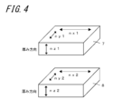
- the half-wave plate has nx1> nz1> ny1 where nx1 and ny1 are in-plane refractive indexes in the directions orthogonal to each other and nz1 is the refractive index in the thickness direction.
- FIG. 1 is a cross-sectional view showing a configuration of a liquid crystal display device according to an embodiment of the present invention.
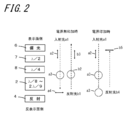
- FIG. 6 is a diagram for explaining the operation of the liquid crystal display device of one embodiment when no electric field is applied and when an electric field is applied. It is a figure which shows the axial arrangement
- FIG. 11 is a diagram for explaining operations of a liquid crystal display device of another embodiment when no electric field is applied and when an electric field is applied. It is a figure which shows the axial arrangement
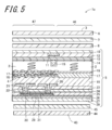
- FIG. 1 is a cross-sectional view showing a configuration of a liquid crystal display device according to an embodiment of the present invention
- FIG. 2 is a diagram for explaining operations of the liquid crystal display device when no electric field is applied and when an electric field is applied.
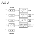
- FIG. 4 is a diagram showing an axial arrangement and a retardation value of the liquid crystal display device
- FIG. 4 is a diagram showing a relationship between respective refractive indexes of the half-wave plate and the first quarter-wave plate of the present invention.
- the liquid crystal display device 1 of the present embodiment shown in FIGS. 1 to 4 is a birefringence control type reflection type liquid crystal display device that displays normally white.
- This liquid crystal display device 1 has a liquid crystal layer 2, and a liquid crystal display panel 5 having a light reflection layer 4 that reflects light that has entered from the display surface 3 side and passed through the liquid crystal layer 2, and a display of the liquid crystal display panel 5.
- the first polarizing plate 6 arranged on the side of the surface 3 and the half-wave plate 7 and the first quarter-wave plate 8 arranged between the liquid crystal display panel 5 and the first polarizing plate 6.
- a polarizing plate with an optical compensation layer for suppressing the above and an image display device using the same.
- a technology that makes both the reflective area and the transmissive area normally white, and a technology that prevents black floating in a wide band on an electrically controlled birefringence (ECB) type liquid crystal display device and further improves the viewing angle Is not specifically proposed.
- liquid crystal molecules are parallel to the surface of the substrate in a state where no electric field is applied to the liquid crystal layer (initial alignment state), and when the electric field applied to this liquid crystal layer is gradually increased, a certain threshold When the electric field is exceeded, the liquid crystal molecules start to rise gradually with respect to the surface of the substrate, and are driven in an operation mode in which the molecular orientation direction is perpendicular to the surface of the substrate at a high voltage.
- a black level having a high display quality is realized in a wide band when an electric field is applied, black floating is suppressed, and a display quality is improved when no electric field is applied.
- the purpose is to achieve a high white level.
- the liquid crystal layer 2 in the light reflecting portion 47 has a phase difference smaller than 1/2 of the phase difference of the half-wave plate 7, and the slow axis of the first quarter-wave plate 8 is the one when no electric field is applied. It intersects with the alignment axis of liquid crystal molecules.
- the half-wave plate 7 has nx1> nz1> ny1, where nx1 and ny1 are the refractive indices in the directions orthogonal to each other in the plane, and nz1 is the refractive index in the thickness direction.
- nx2 and ny2 are the refractive indices in the directions orthogonal to each other and nz2 is the refractive index in the thickness direction.
- the liquid crystal display panel 5 includes a first substrate 10, a light shielding layer 11, a color filter layer 12, a common electrode 13, a first alignment layer 14, a columnar portion 15, a liquid crystal layer 2, a second alignment layer 16, and a transparent electrode 17. , Fifth interlayer insulating layer 18, light reflecting layer 4, fourth interlayer insulating layer 19, drain electrode 20, source electrode 21, interlayer connecting portion 22, third interlayer insulating layer 23, second interlayer insulating layer 24.
- the drain electrode 20, the source electrode 21, the interlayer connection portion 22, the channel portion 29, the semiconductor layer 30, and the gate electrode 31 described above constitute a thin film transistor (abbreviated as TFT) as an active element.
- the drain electrode 20 is connected to the light reflection layer 4, which is a pixel electrode, by an interlayer connection portion 22 or the like.
- the gate signal line connected to the gate electrode 31 is provided for each row in the pixel group arranged in a matrix, and the source signal line connected to the source electrode 21 is provided for each column in the pixel group arranged in a matrix. And a pixel is formed corresponding to each intersection of the gate signal line and the source signal line.
- the first substrate 10 and the second substrate 28 are realized by glass substrates.
- the light-shielding layer 11 constitutes a black matrix, is provided between pixels in a plan view seen from above in FIG. 1, and partitions each pixel.
- the common electrode 13 is made of indium tin oxide (abbreviated as ITO) or the like and constitutes a transparent electrode layer.
- the first alignment layer 14 and the second alignment layer 16 are made of polyimide or the like.
- the fourth interlayer insulating layer 19 is made of acrylic resin or the like.
- the first to third interlayer insulating layers 25, 24, 23 and the first and second gate insulating layers 26, 27 are made of silicon oxide (SiO) or silicon nitride (SiN).
- the light reflection layer 4 is made of molybdenum (Mo), aluminum (Al), or the like, and has, for example, a configuration in which an Al layer is laminated on the Mo layer.
- the thin film transistor has a semiconductor layer 30 made of amorphous silicon (a-Si), low-temperature polycrystalline silicon (LTPS), or the like, and is a three-terminal element including a gate electrode 31, a source electrode 21, and a drain electrode 20. Therefore, by applying a voltage of a predetermined potential (for example, 3V, 6V) to the gate electrode 31, a current flows through the semiconductor layer 30 (channel) between the source electrode 21 and the drain electrode 20, and a switching element (gate Function as a transfer element).
- a predetermined potential for example, 3V, 6V
- the liquid crystal display panel 5 is an electrically controlled birefringence (abbreviated as ECB) type, and the liquid crystal molecules are in an initial alignment state in which an electric field is not applied to the liquid crystal layer 2 and the liquid crystal molecules of the first and second substrates 10 and 28. Those subjected to a horizontal alignment treatment so as to be parallel to the surfaces facing each other are used.
- the voltage applied to the liquid crystal display panel 5 is gradually increased, the liquid crystal molecules gradually start rising on the respective surfaces of the first and second substrates 10 and 28 when a certain threshold voltage is exceeded, At a high voltage equal to or higher than the specified value, the molecular orientation direction becomes perpendicular to the surfaces of the substrates 10 and 28.
- liquid crystal is a refractive index anisotropic medium
- the traveling speed differs between the light wave in the alignment axis direction of the liquid crystal molecules (X axis) and the light wave in the direction orthogonal to the alignment axis of the liquid crystal molecules (Y axis).
- the refractive index of the light wave is different between the X axis and the Y axis.
- the light waves that have entered the liquid crystal layer 2 and exited from the liquid crystal layer 2 have different velocities on the X axis and the Y axis, and thus have a phase shift between the X axis and the Y axis. This phase shift is called a phase difference or retardation.
- the present inventor has found that the liquid crystal layer 2 has a phase difference of 1 ⁇ 2 wavelength plate 7 (1/2 wavelength. Is 550 nm, the phase difference is about 275 nm in the half-wave plate 7. In the case where the phase difference is smaller than half of 270 nm in the present embodiment (for example, 112 nm in the present embodiment), a normally white light is obtained. It was found that the tint (degree of whiteness) was good (close to achromatic).
- the present inventor manufactured each sample of the liquid crystal display device of Example 1 and Comparative Example 1 in order to confirm that the visibility of normally white was improved.
- the liquid crystal layer 2 had a retardation value of 112 nm, and a polarizing plate having a product name “TEG1465DUHC” manufactured by Nitto Denko Corporation was used as the first polarizing plate 6.
- a product name “NAZ film” manufactured by Nitto Denko Corporation was used as the half-wave plate 7.
- Nz1 (nx1-nz1) / (nx1-ny1).
- a product name “Zeonor film” manufactured by Nippon Zeon Co., Ltd. was used as the 1 ⁇ 2 wavelength plate 7.
- Nz (nx-nz) / (nx-ny).
- Example 1 and Comparative Example 1 as the first quarter-wave plate 8, a product name “Zeonor film” manufactured by Nippon Zeon Co., Ltd. was used.
- Nz2 (nx2-nz2) / (nx2-ny2).
- CM-2600d manufactured by Konica Minolta Japan Co., Ltd. was used, and reflectance of black display when an electric field was applied and white when no electric field was applied. The display reflectance and the reflection contrast ratio were measured.
- the reflectance of black display was 0.45%
- the reflectance of white display was 17.5%
- the reflection contrast ratio was 39: 1.
- the reflectance for black display was 0.59%
- the reflectance for white display was 17.8%
- the reflection contrast ratio was 30: 1. From this, it was confirmed that the sample of Example 1 had good visibility in black display.
- the retardation of the liquid crystal layer 2 was made smaller than 1/2 of the retardation of the half-wave plate 7, it was possible to obtain a white level with a high display quality and the visibility of white display was improved.
- the retardation of the liquid crystal layer 2 is not less than 1 ⁇ 4 and not less than 1 ⁇ 2 of the retardation of the first 1 ⁇ 2 wavelength plate 7.
- the retardation of the liquid crystal layer 2 is preferably set in the range of 1 ⁇ 4 or more and 4/9 or less of the retardation of the first 1 ⁇ 2 wavelength plate 7, and in this case, the display quality is further improved. It can have a high white level.
- the half-wave plate 7 preferably has a refractive index in the plane orthogonal to each other of nx1 and ny1 (nx1> ny1), and when the refractive index in the thickness direction is nz1, it is smaller than ny1.
- nz1 is set to be large (nx1> nz1> ny1)
- the first quarter-wave plate 8 is a uniaxial film, and it is preferable that the in-plane refractive indices in the directions orthogonal to each other be nx2 and ny2, and that the thickness direction refractive index be nz2.
- Nz2 (nx2-nz2) / (nx2-ny2) is set in the range of 0.8 or more and 1.2 or less.
- a normally white display having a wider viewing angle and a higher display quality can be realized. That is, when an electric field is applied, a black level having a high display quality can be realized in a wide band to further suppress black floating, and when an electric field is not applied, a white level having a higher display quality can be realized.
- the slow axis of the first quarter-wave plate 8 and the alignment axis of the liquid crystal molecules when no electric field is applied intersect at approximately 45 °.
- approximately 45 ° means a range of about 45 ° ⁇ 5 °. Outside this range, problems such as black floating and lowering of contrast tend to occur.
- linearly polarized light a2 passes through the half-wave plate 7 and the first quarter-wave plate 8, the linearly polarized light a2 becomes broadband circularly polarized light (which is referred to as circularly polarized light a3).
- the phase difference of the liquid crystal layer 2 becomes 0, so that the broadband circularly polarized light a3 passes through the half-wave plate 7 and the first quarter-wave plate 8.
- the reflected light also passes through the liquid crystal layer 2 as the broadband circularly polarized light a3 and is reflected by the light reflection layer 4.
- the reflected light b4 of the broadband circularly polarized light a3 passes through the liquid crystal layer 2, the first quarter-wave plate 8 and the half-wave plate 7 again, and is a straight line orthogonal to the polarization direction of the first polarizing plate 6.
- the polarized light b5 is obtained, and a black display with a high display quality, that is, a black display in which so-called black floating is suppressed can be obtained.
- FIG. 5 is a cross-sectional view showing a liquid crystal display device 1a according to another embodiment of the present invention
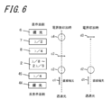
- FIG. 6 is a diagram for explaining the operation of the liquid crystal display device 1a when no electric field is applied and when an electric field is applied.
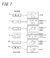
- 7 is a diagram showing the axial arrangement of the liquid crystal display device 1a.
- the parts corresponding to those in the above-described embodiment are designated by the same reference numerals, and the duplicated description will be omitted.
- the liquid crystal display device 1 a shown in FIG. 5 has the same phase difference between the liquid crystal layer 2 in the light reflecting section 47 and the liquid crystal layer 2 in the light transmitting section 46.
- the liquid crystal display device 1 a of the present embodiment is arranged between the liquid crystal display panel 5 and the second polarizing plate 44, and the second polarizing plate 44 arranged on the side opposite to the display surface 43 of the liquid crystal display panel 5. And a second quarter-wave plate 45.
- a light transmitting portion 46 that transmits light incident from the side opposite to the display surface 43 of the liquid crystal display panel 5 is provided in the liquid crystal layer 2, and is a so-called semi-transmissive type (a light reflecting portion and a light transmitting portion). It is realized as a liquid crystal display device including both. Basically, the backlight device is not required on the side opposite to the display surface 43, but it may be provided.
- the second quarter-wave plate 45 its slow axis and the alignment axis of liquid crystal molecules when no electric field is applied intersect at approximately 45 °.
- the above-mentioned approximately 45 ° means a range of about 45 ° ⁇ 5 °. Outside this range, there is a tendency for the problem of lowering of contrast to occur.
- the liquid crystal display panel 5 includes a light transmission portion 46 in the liquid crystal layer 2 that transmits light incident from the side opposite to the display surface 43. Then, as shown in FIG. 6, when the electric field is not applied to the liquid crystal layer 2, the light incident from the side opposite to the display surface 43 of the liquid crystal display panel 5 is converted into linearly polarized light c 1 by the second polarizing plate 44. Become. The linearly polarized light c1 becomes circularly polarized light c2 when passing through the second quarter-wave plate 45.
- the circularly polarized light c2 passes through the liquid crystal layer 2 to become linearly polarized light c3, and after passing through the first 1 ⁇ 4 wavelength plate 8 and the 1 ⁇ 2 wavelength plate 7, becomes circularly polarized light or elliptically polarized light c4.
- the circularly polarized light or the elliptically polarized light c4 passes through only the light in the polarization direction of the first polarizing plate 6 and becomes a white display.
- the angle ⁇ p1 of the absorption axis of the first polarizing plate 6 is 140 °.
- As the second quarter-wave plate 45 a product name “Zeonor film” manufactured by Nippon Zeon Co., Ltd. was used.
- Nz (nx-nz) / (nx-ny).
- a product name “TEG1465DUHC” manufactured by Nitto Denko Corporation was used.
- the slow axis of the second quarter-wave plate 45 and the alignment axis of the liquid crystal molecules when no electric field is applied are approximately 45 °, and the slow axis of the second quarter-wave plate 50 and the first axis
- the slow axis of the quarter-wave plate 8 is selected to be substantially parallel. As a result, it is possible to achieve a normally white, high display quality black level when an electric field is applied.
- the above-mentioned approximately 45 ° means a range of about 45 ° ⁇ 5 °. Outside this range, there is a tendency for the problem of lowering of contrast to occur.
- the phase difference of the light transmitting portion 46 is made larger than that of the light reflecting portion 47 so that the light transmitting portion 46 and the light reflecting portion 47 of the liquid crystal layer 2 have a multi-gap, that is, the liquid crystal layer 2 A layer thickness adjusting layer can be provided.
- the phase difference of the liquid crystal layer 2 in the light transmitting section 46 can be made larger than that of the liquid crystal layer 2 in the light reflecting section 47. It is preferable to set the retardation of the liquid crystal layer 2 in the light transmitting portion 46 to a range of more than 1 time and less than 2 times the retardation of the liquid crystal layer 2 in the light reflecting portion 47.
- the phase difference of the liquid crystal layer 2 in the light transmitting portion 46 is set to be in the range of 1 ⁇ 3 or more and 8/9 or less of the phase difference of the 1 ⁇ 2 wavelength plate 7.
- the retardation of the liquid crystal layer 2 in the light transmitting portion 46 is less than 1 ⁇ 3 of the retardation of the half-wave plate 7, the transmittance and the contrast of the light transmitting portion 46 are likely to decrease. ..
- the retardation of the liquid crystal layer 2 in the light transmitting portion 46 exceeds 8/9 of the retardation of the half-wave plate 7, the contrast tends to decrease in the light transmitting portion 46.
- the phase difference of the liquid crystal layer 2 in the light transmitting portion 46 is set to be approximately twice the phase difference of the liquid crystal layer 2 in the light reflecting portion 47, and the phase difference of the liquid crystal layer 2 in the light transmitting portion 46 is set. It is preferable to set it in the range of 1 ⁇ 2 or more and 8/9 or less of the phase difference of the 1 ⁇ 2 wavelength plate 7.
- Liquid crystal display device Liquid crystal layer 3 Display surface 4 Light reflection layer 5 Liquid crystal display panel 6 First polarizing plate 7 1/2 wavelength plate 8 First 1/4 wavelength plate 10 First substrate 11 Light shielding layer 12 Color Filter Layer 13 Common Electrode 14 First Alignment Layer 15 Columnar Part 16 Second Alignment Layer 17 Transparent Electrode 18 Fifth Interlayer Insulation Layer 19 Fourth Interlayer Insulation Layer 20 Drain Electrode 21 Source Electrode 22 Interlayer Connection 23 Third interlayer insulating layer 24 Second interlayer insulating layer 25 First interlayer insulating layer 26 Second gate insulating layer 27 First gate insulating layer 28 Second substrate 29 Channel part 30 Semiconductor layer 31 Gate electrode 43 Reversal Display surface 44 Second polarizing plate 45 Second quarter-wave plate 46 Light transmitting portion 47 Light reflecting portion
Landscapes
- Physics & Mathematics (AREA)
- Nonlinear Science (AREA)
- Chemical & Material Sciences (AREA)
- Crystallography & Structural Chemistry (AREA)
- General Physics & Mathematics (AREA)
- Optics & Photonics (AREA)
- Mathematical Physics (AREA)
- Liquid Crystal (AREA)
Abstract
La présente invention concerne un dispositif d'affichage à cristaux liquides de type à commande de biréfringence pour réaliser un affichage normalement blanc, selon lequel un large spectre et un niveau noir avec une qualité d'affichage élevée sont réalisés et un affichage noir brillant est supprimé, et un niveau de blanc avec une qualité d'affichage élevée est également réalisé. Un dispositif d'affichage à cristaux liquides de type à commande de biréfringence pour réaliser un affichage normalement blanc, le dispositif étant pourvu d'un panneau d'affichage à cristaux liquides 5 ayant une partie de réflexion de lumière 47, une première plaque de polarisation 6 disposée sur un côté de la surface d'affichage 3 et une plaque de demie longueur d'onde 7 et une première plaque de quart de longueur d'onde 8 qui sont disposées entre le panneau d'affichage à cristaux liquides 5 et la première plaque de polarisation 6, la différence de phase d'une couche de cristaux liquides 2 dans la partie de réflexion de lumière 47 étant inférieure à la moitié de la différence de phase de la plaque de demie de longueur d'onde 7. L'axe lent de la première plaque de quart de longueur d'onde 8 croisant l'axe d'alignement des molécules de cristaux liquides lorsqu'un champ électrique n'est pas appliqué, l'expression nx1 > nz1 > ny1 étant satisfaite, nx1, ny1, et nz1 étant les indices de réfraction à chaque orientation de la plaque de demie de longueur d'onde 7 et l'expression nx2 > nz2 = ny2 étant satisfaite, nx2, ny2 et nz2 étant les indices de réfraction à chaque orientation de la première plaque de quart de longueur d'onde 8.
Priority Applications (4)
| Application Number | Priority Date | Filing Date | Title |
|---|---|---|---|
| EP19876137.1A EP3872560B1 (fr) | 2018-10-25 | 2019-07-12 | Dispositif d'affichage à cristaux liquides |
| US17/283,122 US11275272B2 (en) | 2018-10-25 | 2019-07-12 | Liquid crystal display device |
| JP2020552527A JP7048759B2 (ja) | 2018-10-25 | 2019-07-12 | 液晶表示装置 |
| CN201980067568.6A CN112888995B (zh) | 2018-10-25 | 2019-07-12 | 液晶显示装置 |
Applications Claiming Priority (2)
| Application Number | Priority Date | Filing Date | Title |
|---|---|---|---|
| JP2018200946 | 2018-10-25 | ||
| JP2018-200946 | 2018-10-25 |
Publications (1)
| Publication Number | Publication Date |
|---|---|
| WO2020084845A1 true WO2020084845A1 (fr) | 2020-04-30 |
Family
ID=70332205
Family Applications (1)
| Application Number | Title | Priority Date | Filing Date |
|---|---|---|---|
| PCT/JP2019/027791 Ceased WO2020084845A1 (fr) | 2018-10-25 | 2019-07-12 | Dispositif d'affichage à cristaux liquides |
Country Status (5)
| Country | Link |
|---|---|
| US (1) | US11275272B2 (fr) |
| EP (1) | EP3872560B1 (fr) |
| JP (1) | JP7048759B2 (fr) |
| CN (1) | CN112888995B (fr) |
| WO (1) | WO2020084845A1 (fr) |
Families Citing this family (1)
| Publication number | Priority date | Publication date | Assignee | Title |
|---|---|---|---|---|
| CN114721182A (zh) * | 2022-03-30 | 2022-07-08 | 上海天马微电子有限公司 | 显示面板及显示装置 |
Citations (5)
| Publication number | Priority date | Publication date | Assignee | Title |
|---|---|---|---|---|
| JP2000035570A (ja) * | 1998-07-16 | 2000-02-02 | Sharp Corp | 液晶表示装置 |
| JP2004271786A (ja) * | 2003-03-07 | 2004-09-30 | Hitachi Displays Ltd | 液晶表示装置 |
| JP2007171943A (ja) | 2005-11-28 | 2007-07-05 | Nitto Denko Corp | 光学補償層付偏光板およびそれを用いた画像表示装置 |
| JP2007264586A (ja) * | 2006-02-28 | 2007-10-11 | Nitto Denko Corp | 液晶パネルおよび液晶表示装置 |
| US20100201924A1 (en) * | 2009-02-12 | 2010-08-12 | Yi-Chun Wu | Liquid crystal display |
Family Cites Families (15)
| Publication number | Priority date | Publication date | Assignee | Title |
|---|---|---|---|---|
| GB2342179A (en) * | 1998-09-22 | 2000-04-05 | Sharp Kk | Transflective Liquid Crystal Displays |
| JP3406242B2 (ja) * | 1998-10-15 | 2003-05-12 | シャープ株式会社 | 液晶表示装置 |
| JP2003149636A (ja) * | 2001-11-09 | 2003-05-21 | Sony Corp | 液晶表示装置 |
| JP4228973B2 (ja) * | 2004-04-08 | 2009-02-25 | セイコーエプソン株式会社 | 液晶表示装置および電子機器 |
| CN100397186C (zh) * | 2004-09-16 | 2008-06-25 | 东芝松下显示技术有限公司 | 液晶显示元件 |
| JP2007283601A (ja) * | 2006-04-14 | 2007-11-01 | Sony Corp | 光学シート、バックライト装置および液晶表示装置 |
| JP5252335B2 (ja) * | 2006-10-27 | 2013-07-31 | Nltテクノロジー株式会社 | 液晶表示装置、および端末装置 |
| US20080309854A1 (en) * | 2007-06-15 | 2008-12-18 | Zhibing Ge | Wide Viewing Angle and Broadband Circular Polarizers for Transflective Liquid Crystal Displays |
| JP2009276618A (ja) * | 2008-05-15 | 2009-11-26 | Nitto Denko Corp | 液晶表示装置 |
| WO2010104528A1 (fr) * | 2009-03-09 | 2010-09-16 | Pixel Qi Corporation | Afficheurs à cristaux liquides transflectifs normalement noirs |
| US20120120328A1 (en) * | 2010-11-12 | 2012-05-17 | Ruibo Lu | Transflective Liquid Crystal Displays Using Transverse Electric Field Effect |
| JP2014178454A (ja) * | 2013-03-14 | 2014-09-25 | Japan Display Inc | 液晶表示装置及び電子機器 |
| JP6586276B2 (ja) * | 2015-02-20 | 2019-10-02 | 住友化学株式会社 | 化合物およびこれを含む組成物 |
| JP6818643B2 (ja) * | 2017-06-28 | 2021-01-20 | 京セラ株式会社 | 液晶表示装置 |
| JP7145954B2 (ja) * | 2018-08-17 | 2022-10-03 | 大阪ガスケミカル株式会社 | 位相差フィルム及びその製造方法 |
-
2019
- 2019-07-12 EP EP19876137.1A patent/EP3872560B1/fr active Active
- 2019-07-12 WO PCT/JP2019/027791 patent/WO2020084845A1/fr not_active Ceased
- 2019-07-12 CN CN201980067568.6A patent/CN112888995B/zh active Active
- 2019-07-12 JP JP2020552527A patent/JP7048759B2/ja active Active
- 2019-07-12 US US17/283,122 patent/US11275272B2/en active Active
Patent Citations (5)
| Publication number | Priority date | Publication date | Assignee | Title |
|---|---|---|---|---|
| JP2000035570A (ja) * | 1998-07-16 | 2000-02-02 | Sharp Corp | 液晶表示装置 |
| JP2004271786A (ja) * | 2003-03-07 | 2004-09-30 | Hitachi Displays Ltd | 液晶表示装置 |
| JP2007171943A (ja) | 2005-11-28 | 2007-07-05 | Nitto Denko Corp | 光学補償層付偏光板およびそれを用いた画像表示装置 |
| JP2007264586A (ja) * | 2006-02-28 | 2007-10-11 | Nitto Denko Corp | 液晶パネルおよび液晶表示装置 |
| US20100201924A1 (en) * | 2009-02-12 | 2010-08-12 | Yi-Chun Wu | Liquid crystal display |
Also Published As
| Publication number | Publication date |
|---|---|
| EP3872560A1 (fr) | 2021-09-01 |
| EP3872560A4 (fr) | 2022-06-29 |
| US11275272B2 (en) | 2022-03-15 |
| US20210389630A1 (en) | 2021-12-16 |
| EP3872560B1 (fr) | 2024-04-03 |
| JPWO2020084845A1 (ja) | 2021-09-16 |
| JP7048759B2 (ja) | 2022-04-05 |
| CN112888995B (zh) | 2023-11-07 |
| CN112888995A (zh) | 2021-06-01 |
Similar Documents
| Publication | Publication Date | Title |
|---|---|---|
| CN101617269B (zh) | 视场角控制装置以及具有该视场角控制装置的显示器 | |
| US10473980B2 (en) | In-plane switching mode liquid crystal display device comprising an in-cell retarder and first and second optical compensation films | |
| US8743323B2 (en) | Transmissive liquid crystal display panel comprising a subpixel for display and a subpixel for control of a view angle wherein a light blocking member is formed in a central position of each of a plurality of slit-like openings | |
| US8319922B2 (en) | Liquid crystal display and electronic apparatus | |
| US7643116B2 (en) | Liquid crystal display device | |
| CN100397186C (zh) | 液晶显示元件 | |
| JP2007101874A (ja) | 液晶表示素子 | |
| KR101293564B1 (ko) | 액정표시장치 | |
| JP6818643B2 (ja) | 液晶表示装置 | |
| JP2008014965A (ja) | 液晶表示装置 | |
| JP7048759B2 (ja) | 液晶表示装置 | |
| JP2007304498A (ja) | 液晶表示装置 | |
| US20060114381A1 (en) | Liquid crystal display device with dual modes | |
| JP2008287071A (ja) | 液晶表示装置 | |
| KR20090071082A (ko) | 광학 보상필름을 포함하는 횡전계방식 액정표시장치 | |
| JP6878265B2 (ja) | 液晶表示装置 | |
| JP6882159B2 (ja) | 液晶表示装置 | |
| JP6882225B2 (ja) | 液晶表示装置 | |
| JP2009003432A (ja) | 液晶表示装置 | |
| JP6808576B2 (ja) | 液晶表示装置 | |
| JP6882132B2 (ja) | 液晶表示装置 | |
| JP6769849B2 (ja) | 液晶表示装置 | |
| KR101839332B1 (ko) | 광시야각 액정표시소자 | |
| JP2019061193A (ja) | 液晶表示装置 | |
| JP2005338504A (ja) | 液晶表示素子 |
Legal Events
| Date | Code | Title | Description |
|---|---|---|---|
| 121 | Ep: the epo has been informed by wipo that ep was designated in this application |
Ref document number: 19876137 Country of ref document: EP Kind code of ref document: A1 |
|
| ENP | Entry into the national phase |
Ref document number: 2020552527 Country of ref document: JP Kind code of ref document: A |
|
| NENP | Non-entry into the national phase |
Ref country code: DE |
|
| ENP | Entry into the national phase |
Ref document number: 2019876137 Country of ref document: EP Effective date: 20210525 |