WO2020085256A1 - Procédé de fabrication de dispositif à semi-conducteur - Google Patents
Procédé de fabrication de dispositif à semi-conducteur Download PDFInfo
- Publication number
- WO2020085256A1 WO2020085256A1 PCT/JP2019/041196 JP2019041196W WO2020085256A1 WO 2020085256 A1 WO2020085256 A1 WO 2020085256A1 JP 2019041196 W JP2019041196 W JP 2019041196W WO 2020085256 A1 WO2020085256 A1 WO 2020085256A1
- Authority
- WO
- WIPO (PCT)
- Prior art keywords
- wafer
- group
- semiconductor device
- temporary adhesive
- thinned
- Prior art date
- Legal status (The legal status is an assumption and is not a legal conclusion. Google has not performed a legal analysis and makes no representation as to the accuracy of the status listed.)
- Ceased
Links
Images




Classifications
-
- C—CHEMISTRY; METALLURGY
- C08—ORGANIC MACROMOLECULAR COMPOUNDS; THEIR PREPARATION OR CHEMICAL WORKING-UP; COMPOSITIONS BASED THEREON
- C08G—MACROMOLECULAR COMPOUNDS OBTAINED OTHERWISE THAN BY REACTIONS ONLY INVOLVING UNSATURATED CARBON-TO-CARBON BONDS
- C08G65/00—Macromolecular compounds obtained by reactions forming an ether link in the main chain of the macromolecule
- C08G65/02—Macromolecular compounds obtained by reactions forming an ether link in the main chain of the macromolecule from cyclic ethers by opening of the heterocyclic ring
- C08G65/32—Polymers modified by chemical after-treatment
- C08G65/329—Polymers modified by chemical after-treatment with organic compounds
- C08G65/336—Polymers modified by chemical after-treatment with organic compounds containing silicon
-
- C—CHEMISTRY; METALLURGY
- C09—DYES; PAINTS; POLISHES; NATURAL RESINS; ADHESIVES; COMPOSITIONS NOT OTHERWISE PROVIDED FOR; APPLICATIONS OF MATERIALS NOT OTHERWISE PROVIDED FOR
- C09J—ADHESIVES; NON-MECHANICAL ASPECTS OF ADHESIVE PROCESSES IN GENERAL; ADHESIVE PROCESSES NOT PROVIDED FOR ELSEWHERE; USE OF MATERIALS AS ADHESIVES
- C09J125/00—Adhesives based on homopolymers or copolymers of compounds having one or more unsaturated aliphatic radicals, each having only one carbon-to-carbon double bond, and at least one being terminated by an aromatic carbocyclic ring; Adhesives based on derivatives of such polymers
- C09J125/18—Homopolymers or copolymers of aromatic monomers containing elements other than carbon and hydrogen
-
- C—CHEMISTRY; METALLURGY
- C09—DYES; PAINTS; POLISHES; NATURAL RESINS; ADHESIVES; COMPOSITIONS NOT OTHERWISE PROVIDED FOR; APPLICATIONS OF MATERIALS NOT OTHERWISE PROVIDED FOR
- C09J—ADHESIVES; NON-MECHANICAL ASPECTS OF ADHESIVE PROCESSES IN GENERAL; ADHESIVE PROCESSES NOT PROVIDED FOR ELSEWHERE; USE OF MATERIALS AS ADHESIVES
- C09J129/00—Adhesives based on homopolymers or copolymers of compounds having one or more unsaturated aliphatic radicals, each having only one carbon-to-carbon double bond, and at least one being terminated by an alcohol, ether, aldehydo, ketonic, acetal, or ketal radical; Adhesives based on hydrolysed polymers of esters of unsaturated alcohols with saturated carboxylic acids; Adhesives based on derivatives of such polymers
- C09J129/14—Homopolymers or copolymers of acetals or ketals obtained by polymerisation of unsaturated acetals or ketals or by after-treatment of polymers of unsaturated alcohols
-
- C—CHEMISTRY; METALLURGY
- C09—DYES; PAINTS; POLISHES; NATURAL RESINS; ADHESIVES; COMPOSITIONS NOT OTHERWISE PROVIDED FOR; APPLICATIONS OF MATERIALS NOT OTHERWISE PROVIDED FOR
- C09J—ADHESIVES; NON-MECHANICAL ASPECTS OF ADHESIVE PROCESSES IN GENERAL; ADHESIVE PROCESSES NOT PROVIDED FOR ELSEWHERE; USE OF MATERIALS AS ADHESIVES
- C09J167/00—Adhesives based on polyesters obtained by reactions forming a carboxylic ester link in the main chain; Adhesives based on derivatives of such polymers
- C09J167/02—Polyesters derived from dicarboxylic acids and dihydroxy compounds
-
- C—CHEMISTRY; METALLURGY
- C09—DYES; PAINTS; POLISHES; NATURAL RESINS; ADHESIVES; COMPOSITIONS NOT OTHERWISE PROVIDED FOR; APPLICATIONS OF MATERIALS NOT OTHERWISE PROVIDED FOR
- C09J—ADHESIVES; NON-MECHANICAL ASPECTS OF ADHESIVE PROCESSES IN GENERAL; ADHESIVE PROCESSES NOT PROVIDED FOR ELSEWHERE; USE OF MATERIALS AS ADHESIVES
- C09J171/00—Adhesives based on polyethers obtained by reactions forming an ether link in the main chain; Adhesives based on derivatives of such polymers
- C09J171/02—Polyalkylene oxides
-
- C—CHEMISTRY; METALLURGY
- C09—DYES; PAINTS; POLISHES; NATURAL RESINS; ADHESIVES; COMPOSITIONS NOT OTHERWISE PROVIDED FOR; APPLICATIONS OF MATERIALS NOT OTHERWISE PROVIDED FOR
- C09J—ADHESIVES; NON-MECHANICAL ASPECTS OF ADHESIVE PROCESSES IN GENERAL; ADHESIVE PROCESSES NOT PROVIDED FOR ELSEWHERE; USE OF MATERIALS AS ADHESIVES
- C09J183/00—Adhesives based on macromolecular compounds obtained by reactions forming in the main chain of the macromolecule a linkage containing silicon, with or without sulfur, nitrogen, oxygen, or carbon only; Adhesives based on derivatives of such polymers
- C09J183/04—Polysiloxanes
-
- H—ELECTRICITY
- H10—SEMICONDUCTOR DEVICES; ELECTRIC SOLID-STATE DEVICES NOT OTHERWISE PROVIDED FOR
- H10P—GENERIC PROCESSES OR APPARATUS FOR THE MANUFACTURE OR TREATMENT OF DEVICES COVERED BY CLASS H10
- H10P52/00—Grinding, lapping or polishing of wafers, substrates or parts of devices
-
- H—ELECTRICITY
- H10—SEMICONDUCTOR DEVICES; ELECTRIC SOLID-STATE DEVICES NOT OTHERWISE PROVIDED FOR
- H10P—GENERIC PROCESSES OR APPARATUS FOR THE MANUFACTURE OR TREATMENT OF DEVICES COVERED BY CLASS H10
- H10P72/00—Handling or holding of wafers, substrates or devices during manufacture or treatment thereof
- H10P72/70—Handling or holding of wafers, substrates or devices during manufacture or treatment thereof for supporting or gripping
- H10P72/74—Handling or holding of wafers, substrates or devices during manufacture or treatment thereof for supporting or gripping using temporarily an auxiliary support
-
- H—ELECTRICITY
- H10—SEMICONDUCTOR DEVICES; ELECTRIC SOLID-STATE DEVICES NOT OTHERWISE PROVIDED FOR
- H10P—GENERIC PROCESSES OR APPARATUS FOR THE MANUFACTURE OR TREATMENT OF DEVICES COVERED BY CLASS H10
- H10P95/00—Generic processes or apparatus for manufacture or treatments not covered by the other groups of this subclass
- H10P95/11—Separation of active layers from substrates
-
- H—ELECTRICITY
- H10—SEMICONDUCTOR DEVICES; ELECTRIC SOLID-STATE DEVICES NOT OTHERWISE PROVIDED FOR
- H10W—GENERIC PACKAGES, INTERCONNECTIONS, CONNECTORS OR OTHER CONSTRUCTIONAL DETAILS OF DEVICES COVERED BY CLASS H10
- H10W20/00—Interconnections in chips, wafers or substrates
- H10W20/01—Manufacture or treatment
- H10W20/021—Manufacture or treatment of interconnections within wafers or substrates
- H10W20/023—Manufacture or treatment of interconnections within wafers or substrates the interconnections being through-semiconductor vias
-
- H—ELECTRICITY
- H10—SEMICONDUCTOR DEVICES; ELECTRIC SOLID-STATE DEVICES NOT OTHERWISE PROVIDED FOR
- H10W—GENERIC PACKAGES, INTERCONNECTIONS, CONNECTORS OR OTHER CONSTRUCTIONAL DETAILS OF DEVICES COVERED BY CLASS H10
- H10W20/00—Interconnections in chips, wafers or substrates
- H10W20/01—Manufacture or treatment
- H10W20/021—Manufacture or treatment of interconnections within wafers or substrates
- H10W20/023—Manufacture or treatment of interconnections within wafers or substrates the interconnections being through-semiconductor vias
- H10W20/0245—Manufacture or treatment of interconnections within wafers or substrates the interconnections being through-semiconductor vias comprising use of blind vias during the manufacture
-
- H—ELECTRICITY
- H10—SEMICONDUCTOR DEVICES; ELECTRIC SOLID-STATE DEVICES NOT OTHERWISE PROVIDED FOR
- H10W—GENERIC PACKAGES, INTERCONNECTIONS, CONNECTORS OR OTHER CONSTRUCTIONAL DETAILS OF DEVICES COVERED BY CLASS H10
- H10W20/00—Interconnections in chips, wafers or substrates
- H10W20/01—Manufacture or treatment
- H10W20/021—Manufacture or treatment of interconnections within wafers or substrates
- H10W20/023—Manufacture or treatment of interconnections within wafers or substrates the interconnections being through-semiconductor vias
- H10W20/0253—Manufacture or treatment of interconnections within wafers or substrates the interconnections being through-semiconductor vias comprising forming the through-semiconductor vias after stacking of the chips, wafers or substrates
-
- H—ELECTRICITY
- H10—SEMICONDUCTOR DEVICES; ELECTRIC SOLID-STATE DEVICES NOT OTHERWISE PROVIDED FOR
- H10W—GENERIC PACKAGES, INTERCONNECTIONS, CONNECTORS OR OTHER CONSTRUCTIONAL DETAILS OF DEVICES COVERED BY CLASS H10
- H10W20/00—Interconnections in chips, wafers or substrates
- H10W20/20—Interconnections within wafers or substrates, e.g. through-silicon vias [TSV]
-
- H—ELECTRICITY
- H10—SEMICONDUCTOR DEVICES; ELECTRIC SOLID-STATE DEVICES NOT OTHERWISE PROVIDED FOR
- H10W—GENERIC PACKAGES, INTERCONNECTIONS, CONNECTORS OR OTHER CONSTRUCTIONAL DETAILS OF DEVICES COVERED BY CLASS H10
- H10W90/00—Package configurations
-
- C—CHEMISTRY; METALLURGY
- C08—ORGANIC MACROMOLECULAR COMPOUNDS; THEIR PREPARATION OR CHEMICAL WORKING-UP; COMPOSITIONS BASED THEREON
- C08G—MACROMOLECULAR COMPOUNDS OBTAINED OTHERWISE THAN BY REACTIONS ONLY INVOLVING UNSATURATED CARBON-TO-CARBON BONDS
- C08G77/00—Macromolecular compounds obtained by reactions forming a linkage containing silicon with or without sulfur, nitrogen, oxygen or carbon in the main chain of the macromolecule
- C08G77/04—Polysiloxanes
- C08G77/14—Polysiloxanes containing silicon bound to oxygen-containing groups
-
- H—ELECTRICITY
- H10—SEMICONDUCTOR DEVICES; ELECTRIC SOLID-STATE DEVICES NOT OTHERWISE PROVIDED FOR
- H10P—GENERIC PROCESSES OR APPARATUS FOR THE MANUFACTURE OR TREATMENT OF DEVICES COVERED BY CLASS H10
- H10P72/00—Handling or holding of wafers, substrates or devices during manufacture or treatment thereof
- H10P72/70—Handling or holding of wafers, substrates or devices during manufacture or treatment thereof for supporting or gripping
- H10P72/74—Handling or holding of wafers, substrates or devices during manufacture or treatment thereof for supporting or gripping using temporarily an auxiliary support
- H10P72/7412—Handling or holding of wafers, substrates or devices during manufacture or treatment thereof for supporting or gripping using temporarily an auxiliary support the auxiliary support including means facilitating the separation of a device or wafer from the auxiliary support
-
- H—ELECTRICITY
- H10—SEMICONDUCTOR DEVICES; ELECTRIC SOLID-STATE DEVICES NOT OTHERWISE PROVIDED FOR
- H10P—GENERIC PROCESSES OR APPARATUS FOR THE MANUFACTURE OR TREATMENT OF DEVICES COVERED BY CLASS H10
- H10P72/00—Handling or holding of wafers, substrates or devices during manufacture or treatment thereof
- H10P72/70—Handling or holding of wafers, substrates or devices during manufacture or treatment thereof for supporting or gripping
- H10P72/74—Handling or holding of wafers, substrates or devices during manufacture or treatment thereof for supporting or gripping using temporarily an auxiliary support
- H10P72/7416—Handling or holding of wafers, substrates or devices during manufacture or treatment thereof for supporting or gripping using temporarily an auxiliary support used during dicing or grinding
-
- H—ELECTRICITY
- H10—SEMICONDUCTOR DEVICES; ELECTRIC SOLID-STATE DEVICES NOT OTHERWISE PROVIDED FOR
- H10P—GENERIC PROCESSES OR APPARATUS FOR THE MANUFACTURE OR TREATMENT OF DEVICES COVERED BY CLASS H10
- H10P72/00—Handling or holding of wafers, substrates or devices during manufacture or treatment thereof
- H10P72/70—Handling or holding of wafers, substrates or devices during manufacture or treatment thereof for supporting or gripping
- H10P72/74—Handling or holding of wafers, substrates or devices during manufacture or treatment thereof for supporting or gripping using temporarily an auxiliary support
- H10P72/744—Details of chemical or physical process used for separating the auxiliary support from a device or a wafer
-
- H—ELECTRICITY
- H10—SEMICONDUCTOR DEVICES; ELECTRIC SOLID-STATE DEVICES NOT OTHERWISE PROVIDED FOR
- H10W—GENERIC PACKAGES, INTERCONNECTIONS, CONNECTORS OR OTHER CONSTRUCTIONAL DETAILS OF DEVICES COVERED BY CLASS H10
- H10W72/00—Interconnections or connectors in packages
- H10W72/071—Connecting or disconnecting
- H10W72/073—Connecting or disconnecting of die-attach connectors
- H10W72/07331—Connecting techniques
- H10W72/07337—Connecting techniques using a polymer adhesive, e.g. an adhesive based on silicone or epoxy
- H10W72/07338—Connecting techniques using a polymer adhesive, e.g. an adhesive based on silicone or epoxy hardening the adhesive by curing, e.g. thermosetting
-
- H—ELECTRICITY
- H10—SEMICONDUCTOR DEVICES; ELECTRIC SOLID-STATE DEVICES NOT OTHERWISE PROVIDED FOR
- H10W—GENERIC PACKAGES, INTERCONNECTIONS, CONNECTORS OR OTHER CONSTRUCTIONAL DETAILS OF DEVICES COVERED BY CLASS H10
- H10W72/00—Interconnections or connectors in packages
- H10W72/30—Die-attach connectors
-
- H—ELECTRICITY
- H10—SEMICONDUCTOR DEVICES; ELECTRIC SOLID-STATE DEVICES NOT OTHERWISE PROVIDED FOR
- H10W—GENERIC PACKAGES, INTERCONNECTIONS, CONNECTORS OR OTHER CONSTRUCTIONAL DETAILS OF DEVICES COVERED BY CLASS H10
- H10W72/00—Interconnections or connectors in packages
- H10W72/30—Die-attach connectors
- H10W72/351—Materials of die-attach connectors
- H10W72/353—Materials of die-attach connectors not comprising solid metals or solid metalloids, e.g. ceramics
- H10W72/354—Materials of die-attach connectors not comprising solid metals or solid metalloids, e.g. ceramics comprising polymers
-
- H—ELECTRICITY
- H10—SEMICONDUCTOR DEVICES; ELECTRIC SOLID-STATE DEVICES NOT OTHERWISE PROVIDED FOR
- H10W—GENERIC PACKAGES, INTERCONNECTIONS, CONNECTORS OR OTHER CONSTRUCTIONAL DETAILS OF DEVICES COVERED BY CLASS H10
- H10W90/00—Package configurations
- H10W90/20—Configurations of stacked chips
- H10W90/297—Configurations of stacked chips characterised by the through-semiconductor vias [TSVs] in the stacked chips
Definitions
- the present invention relates to a method for manufacturing a semiconductor device having a laminated structure including a plurality of semiconductor elements.
- Lamination of each semiconductor wafer in the WOW process is proceeded as follows, for example.
- semiconductor wafers to be laminated are bonded to a predetermined support substrate via an adhesive.
- the semiconductor wafer has a surface (element formation surface) on which a plurality of semiconductor elements are formed through a transistor formation step, a wiring formation step, and the like and a back surface opposite to the surface, and the element formation surface side is bonded. It is bonded to the supporting substrate via the agent.
- the semiconductor wafer supported by the support substrate is thinned by grinding the back surface side thereof.
- the present invention has been devised under the circumstances as described above, and an object thereof is to provide a semiconductor device manufacturing method in which semiconductor elements are multi-layered by stacking wafers in which semiconductor elements are formed.
- the object of the present invention is to provide a method suitable for forming a thin wafer into multiple layers through adhesive bonding while avoiding wafer damage.
- the semiconductor device manufacturing method provided by the present invention includes the following preparation process, thinning process, bonding process, and removal process.
- a reinforcement wafer is prepared.
- the reinforcing wafer has a laminated structure including a wafer having an element formation surface and a back surface opposite to the element formation surface, a support substrate, and a temporary adhesive layer between the element formation surface side of the wafer and the support substrate.
- the element forming surface of the wafer is a surface on which a plurality of semiconductor elements are formed through a transistor forming step, a wiring forming step, and the like.
- the temporary adhesive layer is for realizing a temporary adhesion state between the supporting substrate and the wafer, and the temporary adhesive for forming the temporary adhesive layer reacts with the polyvalent vinyl ether compound and its vinyl ether group.
- the temporary adhesive layer in the reinforcing wafer is formed by solidifying the above-mentioned polymer in the temporary adhesive interposed between the wafer and the supporting substrate.
- the wafer in such a reinforced wafer is thinned by grinding from the back surface side.
- the thinned wafer is formed while being supported by the supporting substrate.
- the bonding step the element forming surface side of the base wafer having the element forming surface and the back surface opposite to this and the back surface side of the above-mentioned thinned wafer of the reinforcing wafer are bonded via an adhesive.
- the adhesive contains a polymerizable group-containing polyorganosilsesquioxane (that is, a polyorganosilsesquioxane having a polymerizable functional group).
- the main bonding step preferably includes a curing treatment for curing the adhesive at a temperature lower than the softening point of the polymer in the temporary adhesive layer.
- an adhesive is applied to one or both of the joining target surfaces (element forming surface of the base wafer, back surface of the thinned wafer), and the joining target surfaces are bonded via the adhesive, After the bonding, the adhesive is cured. Further, in the bonding step, one or both of the surfaces to be bonded may be treated with a silane coupling agent before applying the adhesive.
- the removal step the temporary adhesion state of the temporary adhesive layer between the supporting substrate and the thinned wafer in the reinforced wafer that has undergone the above-described bonding step is released, and the supporting substrate is removed.
- the removing step preferably includes a softening treatment for softening the temporary adhesive layer at a temperature higher than the softening point of the polymer in the temporary adhesive layer.
- the present semiconductor device manufacturing method includes a bonding step in which wafers are bonded by the adhesive containing a polymerizable group-containing polyorganosilsesquioxane.
- the polymerizable group-containing polyorganosilsesquioxane is suitable for achieving a relatively low polymerization temperature or curing temperature of, for example, about 30 to 200 ° C. and also for achieving high heat resistance after curing. Therefore, the adhesive bonding between wafers by the adhesive containing the polymerizable group-containing polyorganosilsesquioxane realizes high heat resistance in the adhesive layer formed between the wafers, and the curing temperature for forming the adhesive layer. Is suitable for suppressing damage to the elements in the wafer as the adherend by reducing
- the temporary adhesive for forming the temporary adhesive layer has, as described above, a polyvalent vinyl ether compound and two or more hydroxy groups or carboxy groups capable of reacting with the vinyl ether group to form an acetal bond. It contains a compound capable of forming a polymer with a polyvalent vinyl ether compound and a thermoplastic resin.
- the temporary adhesive having such a structure, in the form of the temporary adhesive layer solidified between the support substrate and the wafer, while securing a high adhesive force that can withstand grinding or the like in the thinning step for the wafer, For example, it is suitable for realizing a relatively high softening temperature of about 130 to 250 ° C.
- the above-mentioned temporary adhesive layer in the reinforced wafer used in the bonding step is suitable for achieving such a relatively high softening temperature, and the adhesive (polymerizable group-containing polyorganosyl) used in the same step is used.
- the composite structure that the sesquioxane-containing adhesive) is suitable for achieving the relatively low curing temperature and the high heat resistance after curing as described above has a bonding structure and a detaching process. Suitable for achieving both.
- the composite structure is configured such that the bonding step is performed under a relatively low temperature condition, and a good adhesive of the thinned wafer to the base wafer is maintained while maintaining the temporary bonding state between the supporting substrate and the thinned wafer in the reinforcing wafer. It is suitable for realizing bonding, and the subsequent removal process is performed at a relatively high temperature condition to soften and thin the temporary adhesive layer while maintaining the adhesive bond between the base wafer and the thinned wafer. Suitable for performing the removal of the supporting substrate from the wafer.
- the structure in which the temporary adhesive layer is released from the temporary adhesive state through the softening of the temporary adhesive layer prevents the strong stress from acting locally on the thinned wafer. It is suitable for avoiding or suppressing the damage of the wafer.
- the present semiconductor device manufacturing method is suitable for multilayering a thin wafer through adhesive bonding while avoiding wafer damage.
- thermosetting adhesive containing benzocyclobutene (BCB) is known as an adhesive used for joining semiconductor wafers and joining electronic components.
- BCB-containing thermosetting adhesive In order to properly cure the BCB-containing thermosetting adhesive, high temperature heating of about 220 to 350 ° C. is required. Therefore, when the BCB-containing thermosetting adhesive is used for wafer-to-wafer bonding in the bonding step of the WOW process, In the joining step, it is necessary to heat at a high temperature of about 220 to 350 ° C.
- thermosetting adhesive containing a novolac epoxy resin As an adhesive used for joining semiconductor wafers and joining electronic components, a thermosetting adhesive containing a novolac epoxy resin has been known. Although the novolac-based epoxy resin-containing thermosetting adhesive can be cured at a lower temperature than the BCB-containing thermosetting adhesive, it is used in a semiconductor device manufacturing process such as a lead-free solder reflow step or other high temperature process (for example, 260 When exposed to (280 ° C. to 280 ° C.), there is a problem that the adhesive component is decomposed and the adhesive force is likely to decrease.
- the semiconductor device manufacturing method of the present invention is not a thermosetting adhesive containing BCB or a thermosetting adhesive containing a novolac-based epoxy resin as an adhesive for bonding between wafers, but the above-mentioned polymerizable group-containing polyorganosilsesquioxane.
- the above-mentioned temporary adhesive polyvalent vinyl ether compound and polyvalent vinyl ether compound having two or more hydroxy groups or carboxy groups
- a compound capable of forming a polymer and a thermoplastic resin are employed to provide a method suitable for forming a thin wafer into multiple layers through adhesive bonding while avoiding wafer breakage. .
- This semiconductor device manufacturing method preferably comprises a step of preparing at least one additional reinforcing wafer, a thinning step for each additional reinforcing wafer, an additional bonding step for each additional reinforcing wafer, and an additional bonding step.
- the subsequent removing step is further included.
- the additional reinforcing wafer has a laminated structure including a wafer having an element formation surface and a back surface opposite to the element formation surface, a support substrate, and a temporary adhesive layer between the element formation surface side of the wafer and the support substrate.
- the temporary adhesive layer is formed from the above-mentioned temporary adhesive.
- the wafer in such an additional reinforcing wafer is ground from the back surface side to form a thinning wafer.
- the back surface side of the thinned wafer in the additional reinforcing wafer is attached to the device forming surface side of the thinned wafer on the base wafer by the above adhesive (polymerizable group-containing polyorgano). Bonding via a silsesquioxane-containing adhesive).
- the thinned wafer on the base wafer is a thinned wafer bonded to the base wafer in the above-described bonding process, or a thinned wafer additionally stacked on the thinned wafer in the preceding additional bonding process.
- This step preferably includes a curing treatment for curing the adhesive at a temperature lower than the softening point of the polymer in the temporary adhesive layer.
- an adhesive is applied to one or both of the surfaces to be bonded (element forming surface of one thinned wafer, rear surface of the other thinned wafer), and the adhesive is applied via the adhesive.
- the surfaces to be joined are pasted together, and the adhesive is cured after the pasting.
- a silane coupling agent treatment may be applied to one or both of the joining target surfaces before the application of the adhesive.
- the removal step after the additional bonding step the temporary adhesion state of the additional reinforcing wafer between the support substrate and the thinned wafer by the temporary adhesive layer is released, and the support substrate is removed.
- This step preferably includes a softening treatment for softening the temporary adhesive layer at a temperature higher than the softening point of the polymer in the temporary adhesive layer.
- the present semiconductor device manufacturing method further includes a step of forming a through electrode in the wafer laminated body obtained through the removing step.
- the through electrode formed in this step penetrates through the wafer stack from the element formation surface of the thinned wafer located at one end in the stacking direction of the wafer stack to the element formation surface of the base wafer located at the other end. Is extended.
- the semiconductor elements can be appropriately electrically connected in a short distance. Therefore, the structure is suitable for realizing efficient digital signal processing in a manufactured semiconductor device, is suitable for suppressing attenuation of a high-frequency signal, and is also suitable for suppressing power consumption. It is suitable.
- This semiconductor device manufacturing method preferably further includes a step of thinning the base wafer by grinding the back surface side of the base wafer. By this step, the base wafer can be thinned to a predetermined thickness. Such a configuration is suitable for reducing the thickness of the manufactured semiconductor device.
- This semiconductor device manufacturing method may further include the following through electrode forming step and the subsequent base wafer thinning step.
- the through electrode forming step from the element formation surface of the thinned wafer located at one end in the stacking direction of the wafer stack obtained through the removal step to a position beyond the element formation surface of the base wafer located at the other end in the wafer stack. It extends through.
- the base wafer thinning process after the through electrode forming process the base wafer is thinned by grinding the back surface side of the base wafer to expose the through electrodes on the back surface side.
- the through electrode is exposed on the element formation surface of the thinned wafer located at one end in the wafer stacking direction and on the back surface of the base wafer located at the other end in the wafer stacking direction. It will be exposed.
- Such a configuration is suitable for a semiconductor device to be manufactured in order to make the device thinner and to appropriately electrically connect the semiconductor elements in a short distance.
- the present method is preferably applied to a thinned wafer located at one end in the stacking direction in the wafer stack obtained through one base wafer thinning step.
- the method further includes the step of joining the element formation surface side and the element formation surface side of the thinned wafer located at one end in the stacking direction of the wafer stack obtained through another base wafer thinning step (face-to-face). -Face joining).
- the present method is obtained by performing the element forming surface side of the thinned wafer located at one end in the stacking direction of the wafer stacked body obtained through one base wafer thinning step and another base wafer thinning step.
- the method may further include a step of joining to a back surface side of the base wafer located at one end in the laminating direction of the wafer laminated body to be formed (face-to-back joining).
- the present method includes a back surface side of a base wafer located at one end in the stacking direction of a wafer stack obtained through one base wafer thinning step, and a wafer stack obtained through another base wafer thinning step.
- the method may further include a step of bonding the back surface side of the base wafer located at one end of the body in the stacking direction (back-to-back bonding).
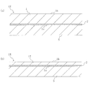
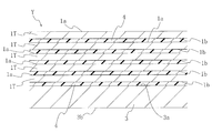
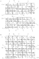
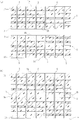
- 3 shows some steps in the semiconductor device manufacturing method according to the embodiment of the present invention.
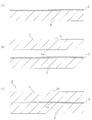
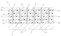
- 3 shows some steps in the semiconductor device manufacturing method according to the embodiment of the present invention.
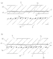
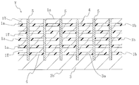
- 3 shows some steps in the semiconductor device manufacturing method according to the embodiment of the present invention.
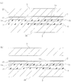
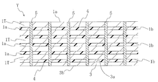
- 3 shows some steps in the semiconductor device manufacturing method according to the embodiment of the present invention.
- 3 shows some steps in the semiconductor device manufacturing method according to the embodiment of the present invention.
- 3 shows some steps in the semiconductor device manufacturing method according to the embodiment of the present invention.
- 3 shows some steps in the semiconductor device manufacturing method according to the embodiment of the present invention.
- 3 shows some steps in the semiconductor device manufacturing method according to the embodiment of the present invention.
- 3 shows some steps in the semiconductor device manufacturing method according to the embodiment of the present invention.
- 3 shows some steps in the semiconductor device manufacturing method according to the embodiment of the present invention. 3 shows some steps in the semiconductor device manufacturing method according to the embodiment of the present invention. 3 shows some steps in the semiconductor device manufacturing method according to the embodiment of the present invention. 3 shows some steps in the semiconductor device manufacturing method according to the embodiment of the present invention. 3 shows some steps in the semiconductor device manufacturing method according to the embodiment of the present invention.
- FIGS. 1 to 9 show a semiconductor device manufacturing method according to an embodiment of the present invention.
- This manufacturing method is a method for manufacturing a semiconductor device having a three-dimensional structure in which semiconductor elements are integrated in the thickness direction, and FIGS. 1 to 9 are partial cross-sectional views showing the manufacturing process.
- a reinforcing wafer 1R as shown in FIG. 1A is prepared (preparation process).
- the reinforcing wafer 1R has a laminated structure including the wafer 1, the supporting substrate S, and the temporary adhesive layer 2 between them.
- the wafer 1 is a wafer having a semiconductor wafer body into which semiconductor elements can be formed, and has an element forming surface 1a and a back surface 1b opposite thereto.
- the element formation surface of the wafer is a surface on the side where a plurality of semiconductor elements (not shown) are formed in the wafer through the transistor formation process.
- Each semiconductor element of the wafer 1 has, for example, a multilayer wiring structure portion including exposed electrode pads on its surface.
- the wafer 1 has various semiconductor elements already formed on the element forming surface 1a side, and the wiring structure required for the semiconductor element is formed later on the element forming surface 1a. May be.
- constituent materials for forming the semiconductor wafer body of the wafer 1 include silicon (Si), germanium (Ge), silicon carbide (SiC), gallium arsenide (GaAs), gallium nitride (GaN), and indium phosphide (InP). ) Is mentioned.
- the thickness of such a wafer 1 is preferably 1000 ⁇ m or less, more preferably 900 ⁇ m or less, and still more preferably 800 ⁇ m or less from the viewpoint of shortening the grinding time in the grinding process described later.
- the thickness of the wafer 1 is, for example, 500 ⁇ m or more.
- the supporting substrate S in the reinforcing wafer 1R is for reinforcing the wafer 1 which becomes thin through the thinning process described below.
- the support substrate S include a silicon wafer and a glass wafer.
- the thickness of the support substrate S is preferably 300 ⁇ m or more, more preferably 500 ⁇ m or more, and more preferably 700 ⁇ m or more from the viewpoint of ensuring the function as a reinforcing element.
- the thickness of the support substrate S is, for example, 800 ⁇ m or less.
- Such a supporting substrate S is bonded to the element forming surface 1a side of the wafer 1 via a temporary adhesive layer 2.
- the temporary adhesive layer 2 is for realizing a temporary adhesive state between the wafer 1 and the supporting substrate S that can be released afterwards.
- the temporary adhesive for forming such a temporary adhesive layer 2 has a polyvalent vinyl ether compound (A) and two or more hydroxy groups or carboxy groups capable of reacting with the vinyl ether group to form an acetal bond. And at least a compound (B) capable of forming a polymer with the polyvalent vinyl ether compound and a thermoplastic resin (C). Each component in the temporary adhesive is specifically described below.
- the reinforced wafer 1R having such a configuration can be manufactured, for example, through the following steps.
- the temporary adhesive layer 2 is formed on the support substrate S.
- a temporary adhesive for forming the temporary adhesive layer 2 is applied onto the supporting substrate S by, for example, spin coating to form a temporary adhesive coating film, and the coating film is dried by heating to perform temporary adhesion.
- the agent layer 2 can be formed.
- the heating temperature is, for example, 100 to 300 ° C. and may be constant or may be changed stepwise.
- the heating time is, for example, 30 seconds to 30 minutes.
- FIGS. 2B and 2C the support substrate S and the wafer 1 are bonded to each other via the temporary adhesive layer 2.
- the wafer 1 has the element forming surface 1a and the back surface 1b opposite thereto, as described above.
- the support substrate S and the wafer 1 are bonded together while being pressed via the temporary adhesive layer 2, and then heated to form a polymer having a softening point in a high temperature range to form a temporary adhesive.
- the layer 2 is solidified, and the supporting substrate S and the wafer 1 are adhered to each other by the temporary adhesive layer 2.
- the applied pressure is, for example, 300 to 5000 g / cm 2
- the temperature is, for example, 30 to 200 ° C.
- the heating temperature is, for example, 100 to 300 ° C., preferably 100 to 250 ° C.
- the heating time is, for example, 30 seconds to 30 minutes, preferably 3 to 12 minutes. It's a minute.
- the heating temperature may be constant or may be changed stepwise.
- the reinforcing wafer 1R having a laminated structure including the wafer 1, the supporting substrate S, and the temporary adhesive layer 2 between them can be manufactured.
- the above-mentioned polyvalent vinyl ether compound (A) in the temporary adhesive is a compound having two or more vinyl ether groups in the molecule and is represented by, for example, the following formula (a).
- Z 1 is a saturated or unsaturated aliphatic hydrocarbon, a saturated or unsaturated alicyclic hydrocarbon, an aromatic hydrocarbon, a heterocyclic compound, or these are bonded via a single bond or a linking group. It represents a group obtained by removing n 1 hydrogen atoms from the structural formula of a bonded conjugate. Further, in the formula (a), n 1 represents an integer of 2 or more, for example, an integer of 2 to 5, preferably an integer of 2 to 3.
- the groups obtained by removing 2 hydrogen atoms from the structural formula of saturated or unsaturated aliphatic hydrocarbon include For example, a linear or branched alkylene group such as methylene group, ethylene group, propylene group, trimethylene group, tetramethylene group, pentamethylene group, hexamethylene group, octamethylene group, decamethylene group, and dodecamethylene group, and Examples thereof include linear or branched alkenylene groups such as a vinylene group, a 1-propenylene group, and a 3-methyl-2-butenylene group.
- a linear or branched alkylene group such as methylene group, ethylene group, propylene group, trimethylene group, tetramethylene group, pentamethylene group, hexamethylene group, octamethylene group, decamethylene group, and dodecamethylene group
- Examples thereof include linear or branched alkenylene groups such as a vinylene group, a 1-propenylene group,
- the alkylene group has, for example, 1 to 20 carbon atoms, and preferably 1 to 10 carbon atoms.
- the alkenylene group has, for example, 2 to 20 carbon atoms, and preferably 2 to 10 carbon atoms.
- Examples of the group obtained by removing three or more hydrogen atoms from the structural formula of a saturated or unsaturated aliphatic hydrocarbon include a group obtained by further removing one or more hydrogen atoms from the structural formulas of these exemplified groups. it can.
- the groups obtained by removing n 1 hydrogen atoms from the structural formula of the saturated or unsaturated alicyclic hydrocarbon as the groups obtained by removing 2 hydrogen atoms from the structural formula of the saturated or unsaturated alicyclic hydrocarbon.
- Examples of the group obtained by removing three or more hydrogen atoms from the structural formula of a saturated or unsaturated alicyclic hydrocarbon include a group obtained by removing one or more hydrogen atoms from the structural formulas of these exemplified groups. You can
- aromatic hydrocarbon examples include benzene, naphthalene, and anthracene.
- the heterocyclic compound includes an aromatic heterocyclic compound and a non-aromatic heterocyclic compound.
- a heterocyclic compound include heterocyclic compounds containing an oxygen atom as a hetero atom (for example, 5-membered ring such as furan, tetrahydrofuran, oxazole, isoxazole, and ⁇ -butyrolactone, 4-oxo-4H- 6-membered rings such as pyran, tetrahydropyran, and morpholine, condensed rings such as benzofuran, isobenzofuran, 4-oxo-4H-chromene, chroman, and isochroman, and 3-oxatricyclo [4.3.1.14,8] ] Undecan-2-one and 3-oxatricyclo [4.2.1.04,8] nonan-2-one and other bridged rings), heterocyclic compounds containing sulfur atoms as heteroatoms (eg thiophene, 5-membered ring such as thiazole, is
- linking group examples include a divalent to tetravalent hydrocarbon group, a carbonyl group (—CO—), an ether bond (—O—), a sulfide bond (—S—), an ester bond (—COO—), and an amide.
- a bond (-CONH-), a carbonate bond (-OCOO-), a urethane bond (-NHCOO-), a -NR- bond (R represents a hydrogen atom, an alkyl group, or an acyl group), and a plurality of these linked.
- the groups mentioned above can be mentioned.
- examples of the divalent hydrocarbon group include linear or branched chains such as methylene group, methylmethylene group, dimethylmethylene group, ethylene group, propylene group, and trimethylene group.
- Examples of the trivalent hydrocarbon group include groups obtained by further removing one hydrogen atom from the structural formula of the divalent hydrocarbon group.
- Examples of the tetravalent hydrocarbon group include groups obtained by further removing two hydrogen atoms from the structural formula of the above divalent hydrocarbon group.
- Z 1 may have one type or two or more types of substituents.
- substituents include an alkyl group, cycloalkyl group, alkenyl group, cycloalkenyl group, aryl group, hydroxy group, carboxy group, nitro group, amino group, mercapto group, halogen atom, and C substituted with a halogen atom.
- substituents include an alkyl group, cycloalkyl group, alkenyl group, cycloalkenyl group, aryl group, hydroxy group, carboxy group, nitro group, amino group, mercapto group, halogen atom, and C substituted with a halogen atom.
- examples thereof include a 2-10 hydrocarbon group, a hydrocarbon group containing a functional group containing a hetero atom (such as oxygen and sulfur), and a group in which two or more of these groups are bonded.
- alkyl group include C 1-4 alkyl groups such as methyl group and ethy
- Examples of the cycloalkyl group include a C 3-10 cycloalkyl group.
- Examples of the alkenyl group include C 2-10 alkenyl groups such as vinyl group.
- Examples of the cycloalkenyl group include a C 3-10 cycloalkenyl group.
- Examples of the aryl group include C 6-15 aryl groups such as a phenyl group and a naphthyl group.
- Examples of the hydrocarbon group containing a hetero atom-containing functional group include a C 1-4 alkoxy group and a C 2-6 acyloxy group.
- polyvalent vinyl ether compound (A) examples include, for example, 1,4-butanediol divinyl ether, diethylene glycol divinyl ether, triethylene glycol divinyl ether, and the following formulas (a-1) to (a-21). The compound represented by these can be mentioned.
- Z 1 in the polyvalent vinyl ether compound (A) forms a polymer having a high softening point in the above-mentioned temporary adhesive, it is preferably a saturated or unsaturated aliphatic hydrocarbon, or a plurality of such carbonizations.
- Hydrogen is a group in which n 1 hydrogen atoms have been removed from the structural formula of a bond in which a hydrogen atom is bonded via a linking group, more preferably a saturated aliphatic hydrocarbon or a plurality of such hydrocarbons via a linking group.
- the polyvalent vinyl ether compound (A) is most preferably at least one compound selected from the group consisting of 1,4-butanediol divinyl ether, diethylene glycol divinyl ether, and triethylene glycol divinyl ether.
- the compound (B) in the temporary adhesive has a polyvalent group having two or more hydroxy groups or carboxy groups capable of reacting with the vinyl ether group of the polyvalent vinyl ether compound (A) to form an acetal bond.
- X represents a hydroxy group or a carboxy group.
- the n 2 Xs may be the same or different from each other.
- n 2 represents an integer of 1 or more.
- N 2 is preferably from the standpoint of availability in preparation of the above-mentioned temporary adhesive and ease of dissolution in a solvent, and from the viewpoint of forming a polymer having a high softening point in the temporary adhesive. It is an integer of 1 to 3, and more preferably an integer of 1 to 2.
- the number of constitutional units (repeating units) represented by the above formula (b) in the compound (B) is 2 or more, and from the viewpoint of forming a polymer having a high softening point in the above-mentioned temporary adhesive, it is preferable. It is an integer of 2 to 40, more preferably an integer of 10 to 30.
- Z 2 is a saturated or unsaturated aliphatic hydrocarbon, a saturated or unsaturated alicyclic hydrocarbon, an aromatic hydrocarbon, a heterocyclic compound, or these are bonded via a single bond or a linking group.
- the compound (B) is preferably a styrene polymer, a (meth) acrylic polymer, polyvinyl alcohol, a novolac resin, and a resole resin, and more preferably from the following formulas (b-1) to (b-6) It is a compound having two or more at least one structural unit (repeating unit) selected from the group consisting of:
- the proportion of the structural unit represented by the formula (b) in the total amount of the compound (B) is preferably 30% by mass or more, It is more preferably 50% by mass or more, and even more preferably 60% by mass or more.
- the ratio of the structural unit represented by the formula (b) in the total amount of the compound (B) is preferably 30 mol% or more, more preferably 50 mol% or more.
- the proportion of the structural unit represented by the formula (b) in the total amount of the compound (B) is preferably 1% by mass or more, It is more preferably 5% by mass or more, and even more preferably 10% by mass or more.
- the proportion of the constitutional unit represented by the formula (b) being within the above range is suitable for securing a sufficient distance between crosslinking points and a sufficient number of crosslinking points in the compound (B), and therefore,
- the above-mentioned temporary adhesive is suitable for ensuring the weight average molecular weight and the high softening point of the polymer obtained by the polymerization of the compound (B) and the above-mentioned compound (A).
- the temporary adhesive layer 2 formed is suitable for ensuring high adhesion retention under a high temperature environment.
- the compound (B) may be a homopolymer having only the constitutional unit represented by the formula (b), or a copolymer having the constitutional unit represented by the formula (b) and another constitutional unit. May be When the compound (B) is a copolymer, it may be any of a block copolymer, a graft copolymer and a random copolymer.
- the above-mentioned other structural unit in the compound (B) is a structural unit derived from a polymerizable monomer having neither a hydroxy group nor a carboxy group, and examples of the polymerizable monomer include olefins and aromatic vinyl compounds. , Unsaturated carboxylic acid esters, carboxylic acid vinyl esters, and unsaturated dicarboxylic acid diesters.
- olefin examples include chain olefins such as ethylene, propylene, and 1-butene (particularly C 2-12 alkenes), cyclopentene, cyclohexene, cycloheptene, norbornene, 5-methyl-2-norbornene, and tetracyclododecene. And other cyclic olefins (especially C 3-10 cycloalkenes).
- aromatic vinyl compound examples include styrene, vinyltoluene, ⁇ -methylstyrene, 1-propenylbenzene, 1-vinylnaphthalene, 2-vinylnaphthalene, 3-vinylpyridine, 3-vinylfuran, 3-vinylthiophene, Mention may be made of C 6-14 aromatic vinyl compounds such as 3-vinylquinoline, indene, methylindene, ethylindene, and dimethylindene.
- Examples of the unsaturated carboxylic acid ester include ethyl (meth) acrylate, butyl (meth) acrylate, isobutyl (meth) acrylate, 2-ethylhexyl (meth) acrylate, and dicyclopentanyl (meth) acrylate.
- R ′′ is a saturated or unsaturated aliphatic hydrocarbon, a saturated or unsaturated aliphatic hydrocarbon, It represents a group in which one hydrogen atom is removed from the structural formula of an unsaturated alicyclic hydrocarbon, aromatic hydrocarbon, heterocyclic compound, or a bonded product of these bonded through a single bond or a linking group.
- R for example, a monovalent group corresponding to the divalent group mentioned for Z 1 in the above formula (a)).
- carboxylic acid vinyl ester for example , Vinyl acetate, vinyl propionate, vinyl caprylate, and caproic acid C 1-16 fatty acid vinyl esters such as vinyl and the like.
- unsaturated dicarboxylic acid diester for example, diethyl maleate, dibutyl maleate, dioctyl maleate, Mention may be made of maleic acid di-C 1-10 alkyl esters such as 2-ethylhexyl maleic acid and corresponding fumaric acid diesters, which may be used alone or in combination of two or more. can do.
- the compound (B) is a copolymer
- the structural unit represented by the above formula (b) a chain olefin, a cyclic olefin, an aromatic vinyl compound, an unsaturated carboxylic acid ester, a carboxylic acid vinyl ester, And a structural unit derived from at least one polymerizable monomer selected from the group consisting of unsaturated dicarboxylic acid diesters are preferred.
- the softening point (T 1 ) of the compound (B) is, for example, 50 ° C. or higher, preferably 80 ° C. or higher, more preferably 100 ° C. or higher.
- Such a configuration is suitable for realizing a high softening point of a polymer obtained by polymerizing the compound (B) and the polyvalent vinyl ether compound (A).
- T 1 is, for example, 250 ° C. or lower, preferably 200 ° C. or lower, more preferably 150 ° C. or lower is there.
- T 1 can be adjusted, for example, by controlling the weight average molecular weight of the compound (B) (polystyrene conversion value by GPC method).
- the weight average molecular weight of the compound (B) is, for example, 1500 or more, preferably 1800 to 10000, more preferably 2000 to 5000.
- thermoplastic resin (C) in the temporary adhesive is a compound having thermoplasticity and capable of imparting flexibility to the adhesive composition when blended into the adhesive composition.
- a thermoplastic resin (C) include polyvinyl acetal resin, polyester resin, polyurethane resin, polyamide resin, poly (thio) ether resin, polycarbonate resin, polysulfone resin, and polyimide resin.
- polycondensation resins such as resins, polyolefin resins, (meth) acrylic resins, styrene resins, vinyl polymerization resins such as vinyl resins, and resins derived from natural products such as cellulose derivatives. These can be used individually by 1 type or in combination of 2 or more types.
- thermoplastic resin (C) is suitable for imparting flexibility and flexibility to the temporary adhesive layer 2 to be formed, and the temperature is rapidly increased. It is suitable for preventing spontaneous peeling and the occurrence of cracks even under an environment where the temperature changes, and is suitable for ensuring excellent adhesiveness.
- the thermoplastic resin (C) in the temporary adhesive is preferably at least one selected from the group consisting of polyvinyl acetal resin, polyester resin, polyurethane resin, and polyamide resin.
- the temporary adhesive or the temporary adhesive layer 2 there is a case in which flexibility is easily imparted, or a chemical interaction with an adherend such as a wafer is weakened and adhesive residue is left on the adherend after peeling.
- the temporary adhesive preferably contains a polyester resin as the thermoplastic resin (C).
- the temporary adhesive in addition to the viewpoint that flexibility is easily imparted and the adhesive residue on the adherend is easily removed, high adhesion to the adherend is secured. From the viewpoint of that, the temporary adhesive preferably contains both the polyester resin and the polyvinyl acetal resin as the thermoplastic resin (C).
- polyvinyl acetal resin examples include resins having at least a constitutional unit represented by the following formula, which is obtained by reacting polyvinyl alcohol with aldehyde (RCHO).
- RCHO aldehyde
- R in the structural formula is a hydrogen atom, a linear C 1-5 alkyl group, a branched C 2-5 alkyl group, or C
- the compound which is a 6-10 aryl group may be mentioned, and specific examples thereof include formaldehyde, butyraldehyde, and benzaldehyde.
- Such a polyvinyl acetal-based resin may have another structural unit other than the structural unit represented by the following formula.
- the polyvinyl acetal-based resin includes homopolymers and copolymers.
- Specific examples of such a polyvinyl acetal-based resin include polyvinyl formal and polyvinyl butyral. Commercially available products) can be used.
- polyester resin examples include polyesters obtained by polycondensation of a diol component and a dicarboxylic acid component.
- diol component examples include aliphatic C 2-12 diol such as ethylene glycol, polyoxy C 2-4 alkylene glycol such as diethylene glycol, alicyclic C 5-15 diol such as cyclohexanedimethanol, and aromatic C 6 such as bisphenol A. -20 diols.
- dicarboxylic acid component examples include aromatic C 8-20 dicarboxylic acids such as terephthalic acid, aliphatic C 2-40 dicarboxylic acids such as adipic acid, and alicyclic C 8-15 dicarboxylic acids such as cyclohexanedicarboxylic acid.
- polyester-based resin also include polyesters obtained by polycondensation of oxycarboxylic acid.
- oxycarboxylic acid include aliphatic C 2-6 oxycarboxylic acid such as lactic acid and aromatic C 7-19 oxycarboxylic acid such as hydroxybenzoic acid.
- polyester-based resin also include polyesters obtained by ring-opening polymerization of lactone.
- polyester-based resin examples include polyesters containing a urethane bond obtained by the reaction of polyester diol and diisocyanate. Polyester resins include homopolyesters and copolyesters. Further, as the polyester-based resin, for example, a commercially available product having a trade name “Placcel H1P” (manufactured by Daicel Corporation) can be used.
- polyurethane-based resin examples include resins obtained by reacting diisocyanates, polyols and a chain extender used as necessary.
- diisocyanates include aliphatic diisocyanates such as hexamethylene diisocyanate, alicyclic diisocyanates such as isophorone diisocyanate, and aromatic diisocyanates such as tolylene diisocyanate.
- Polyols include polyester diols, polyether diols, and polycarbonate diols.
- chain extender examples include C 2-10 alkylenediol such as ethylene glycol, aliphatic diamine such as ethylenediamine, alicyclic diamine such as isophoronediamine, and aromatic diamine such as phenylenediamine.
- polyamide-based resin examples include, for example, a polyamide obtained by polycondensation of a diamine component and a dicarboxylic acid component, a polyamide obtained by polycondensation of an aminocarboxylic acid, a polyamide obtained by ring-opening polymerization of lactam, and a diamine component.
- a polyester amide obtained by polycondensation of a dicarboxylic acid component and a diol component can be mentioned.
- the diamine component examples include C 4-10 alkylenediamine such as hexamethylenediamine.
- dicarboxylic acid component examples include C 4-20 alkylenedicarboxylic acid such as adipic acid.
- the aminocarboxylic acid examples include C 4-20 aminocarboxylic acid such as ⁇ -aminoundecanoic acid.
- lactam examples include C 4-20 lactam such as ⁇ -laurolactam.
- diol component examples include C 2-12 alkylene diol such as ethylene glycol.
- the polyamide resin includes homopolyamide and copolyamide.
- the softening point (T 2 ) of the thermoplastic resin (C) is the thermosetting temperature of the permanent adhesive described below, which is used in combination with the temporary adhesive containing the thermoplastic resin (C) in the semiconductor device manufacturing method according to the present invention. It is preferably higher by 10 ° C. or more.
- the difference between the thermosetting temperature and T 2 of the permanent adhesive is, for example, 10 to 40 ° C, preferably 20 to 30 ° C.
- T 2 can be adjusted, for example, by controlling the weight average molecular weight (Mw: polystyrene conversion value by GPC method) of the thermoplastic resin (C).
- Mw polystyrene conversion value by GPC method
- the weight average molecular weight of the thermoplastic resin (C) is, for example, 1500 to 100,000, preferably 2,000 to 80,000, more preferably 3,000 to 50,000, more preferably 10,000 to 45,000, and more preferably 15,000 to 35,000.
- the polymer of the polyvalent vinyl ether compound (A) and the compound (B) is softened.
- the point (T 3 ) is preferably higher by 10 ° C. or more than the thermosetting temperature of a permanent adhesive described later used in combination with the temporary adhesive in the semiconductor device manufacturing method according to the present invention.
- the difference between the thermosetting temperature and T 3 of the permanent adhesive is, for example, 10 to 40 ° C, preferably 20 to 30 ° C.
- the content of the polyvalent vinyl ether compound (A) in the temporary adhesive is the total amount of hydroxy groups and carboxy groups in the compound (B) in the temporary adhesive.
- the amount of the vinyl ether group in the polyvalent vinyl ether compound (A) is, for example, 0.01 to 10 mol, preferably 0.05 to 5 mol, more preferably 0.07 to 1 mol, based on 1 mol. The amount is preferably 0.08 to 0.5 mol.
- the content of the thermoplastic resin (C) in the temporary adhesive is, for example, 0.1 to 3 parts by mass, preferably 0.2 to 2 parts by mass, relative to 1 part by mass of the compound (B) in the temporary adhesive. , And more preferably 0.3 to 1 part by mass.
- the total content of the polyvalent vinyl ether compound (A), the compound (B) and the thermoplastic resin (C) in the temporary adhesive is, for example, 70 to 99.9 mass% of the total nonvolatile content of the temporary adhesive, and is preferable. Is 80 to 99% by mass, more preferably 85 to 95% by mass, and even more preferably 85 to 90% by mass.
- the temporary adhesive may further contain a polymerization accelerator.
- the polymerization accelerator include a monovalent carboxylic acid represented by the following formula (d) and a monovalent alcohol represented by the following formula (e). These can be used individually by 1 type or in combination of 2 or more types.
- the configuration in which the temporary adhesive contains a polymerization accelerator is suitable for promoting the polymerization reaction of the polyvalent vinyl ether compound (A) and the compound (B), and when using an adhesive containing no polymerization accelerator.
- Z 3 -COOH (d) (In the formula, Z 3 is selected from the group consisting of a saturated or unsaturated aliphatic hydrocarbon, a saturated or unsaturated alicyclic hydrocarbon, and an aromatic hydrocarbon which may have a substituent other than a carboxy group.
- the saturated or unsaturated aliphatic hydrocarbon, saturated or unsaturated alicyclic hydrocarbon, and aromatic hydrocarbon represented by Z 3 in the above formula (d) are the saturated ones mentioned for Z 1 in the above formula (a).
- the substituent which Z 3 may have include an example in which a carboxy group is removed from the examples of the substituent which Z 1 may have.
- the aromatic hydrocarbon for Z 4 in the above formula (e) the aromatic hydrocarbons mentioned for Z 1 in the above formula (a) can be mentioned.
- the substituent which Z 4 may have include an example in which a hydroxy group is removed from the examples of the substituent which Z 1 may have.
- the pKa (acid dissociation constant) of the polymerization accelerator is preferably 3 to 8, more preferably 4 to 6.
- Such a structure prevents storage of the temporary adhesive agent from unintentionally increasing the viscosity due to unintentional polymerization and ensures storage stability, and at the time of forming the temporary adhesive agent layer 2 from the temporary adhesive agent. It is suitable for ensuring the polymerization promoting effect of the polymerization accelerator.
- the compounds shown below are preferable.
- the content thereof is, for example, about 0.01 to 5 parts by mass, preferably 1 part by mass of the polyvalent vinyl ether compound (A) contained in the temporary adhesive.
- the amount is 0.1 to 3 parts by mass, more preferably 0.3 to 1 part by mass.
- the temporary adhesive may further contain an antioxidant.
- the configuration in which the temporary adhesive contains an antioxidant is suitable for preventing the above-mentioned compound (B) and thermoplastic resin (C) from being oxidized during the heat treatment of the temporary adhesive.
- the antioxidant of the compound (B) and the thermoplastic resin (C) in the temporary adhesive is determined by the solubility of the softening composition obtained by heating the temporary adhesive layer 2 formed from the temporary adhesive in a solvent. Therefore, even if adhesive residue remains on the adherend after the temporary adhesive layer 2 is peeled from the adherend such as a wafer through a heat treatment, the adhesive residue is removed. It is suitable for this.
- antioxidants examples include phenolic antioxidants, phosphorus antioxidants, thioester antioxidants, and amine antioxidants. These can be used alone or in combination of two or more. Phenolic antioxidants are particularly preferable as antioxidants in temporary adhesives because they have a particularly excellent antioxidant effect during heat treatment.
- phenolic antioxidants examples include pentaerythritol tetrakis [3 (3,5-di-t-butyl-4-hydroxyphenyl) propionate] and thiodiethylenebis [3- (3,5-di-t-butyl).
- the content thereof is, for example, 0.01 to about 100 parts by mass of the compound (B) and the thermoplastic resin (C) contained in the temporary adhesive.
- the amount is 15 parts by mass, preferably 0.1 to 12 parts by mass, more preferably 0.5 to 10 parts by mass.
- the temporary adhesive may further contain other components as needed.
- other components include an acid generator, a surfactant, a solvent, a leveling agent, a silane coupling agent, and a foaming agent. These can be used alone or in combination of two or more.
- the content of the surfactant in the temporary adhesive is preferably about 0.01 to 1% by mass.
- a surfactant include, for example, trade names “F-444”, “F-447”, “F-554”, “F-556”, and “F-557” (both are fluorine-based oligomers manufactured by DIC), Product names "BYK-350” (acrylic polymer manufactured by BYK Chemie) and product names "A-1420" "A-1620” "A-1630” (all are fluorine-containing alcohol manufactured by Daikin Industries, Ltd.) Can be mentioned. These can be used alone or in combination of two or more.
- the temporary adhesive preferably contains a solvent from the viewpoint of adjusting its viscosity.
- the solvent include toluene, hexane, isopropanol, methyl isobutyl ketone, cyclopentanone, cyclohexanone, propylene glycol monomethyl ether acetate, propylene glycol monomethyl ether, and ⁇ -butyrolactone. These can be used alone or in combination of two or more.
- the solvent content of the temporary adhesive is, for example, 55 to 80% by mass.
- the temporary adhesive can be prepared by stirring and mixing the constituent components while removing air bubbles under vacuum if necessary.
- the temperature of the mixture at the time of stirring and mixing is preferably about 10 to 80 ° C.
- a rotation-revolution type mixer for example, a single-screw or multi-screw extruder, a planetary mixer, a kneader, or a dissolver can be used.
- the viscosity of the temporary adhesive (viscosity measured under conditions of 25 ° C. and shear rate of 50 / s) is, for example, about 30 to 2000 mPa ⁇ s, preferably 300 to 1500 mPa ⁇ s, and more preferably 500 to 1500 mPa ⁇ s. Is.
- Such a configuration is suitable for securing the coatability of the temporary adhesive and uniformly coating it on the surface of an adherend such as a wafer.
- a polymer can be produced from the polyvalent vinyl ether compound (A) and the compound (B) by acetal-bonding the hydroxy group and / or the carboxy group.
- a tentative compound containing a compound represented by the following formula (a ′) as the polyvalent vinyl ether compound (A) and a compound having a structural unit represented by the following formula (b ′) as the compound (B) A polymer represented by the following formula (P) is obtained by subjecting the adhesive to heat treatment to polymerize both these compounds.
- the softening point (T 3 ) of the polymer obtained by subjecting the temporary adhesive to heat treatment can be controlled by adjusting the relative amounts of the polyvalent vinyl ether compound (A) and the compound (B).
- the softening point (T 3 ) of the polymer is, for example, 130 ° C. or higher, and preferably 130 to 170 ° C., more preferably 140 to 160 ° C.
- the softening points of the above-mentioned polymer of the polyvalent vinyl ether compound (A) and the compound (B), the polyvalent vinyl ether compound (A), the compound (B), and the thermoplastic resin (C) are high under the following flow conditions. It can be measured using a chemical flow tester. ⁇ Flow conditions> Pressure: 100kg / cm 2 Speed: 6 °C / min Nozzle: 1mm ⁇ ⁇ 10mm
- the softening point of the temporary adhesive layer formed from the temporary adhesive shall be the temperature determined as follows. First, 0.1 g of the temporary adhesive is applied to the first glass plate to a thickness of 10 ⁇ m to form a coating film of the temporary adhesive. Next, the 2nd glass plate is piled up on the coating film. Next, through a heat treatment, the polyvalent vinyl ether compound (A) and the compound (B) are polymerized in the temporary adhesive between the first and second glass plates to cure the temporary adhesive, The two glass plates are joined together with an adhesive.
- the heat treatment includes, for example, heating at 140 ° C. for 2 minutes, followed by heating at 200 ° C. for 2 minutes, and then heating at 230 ° C. for 4 minutes.
- a laminated body having a laminated structure of the first glass plate, the second glass plate, and the temporary adhesive layer therebetween can be obtained.
- the first glass plate was pulled by applying a stress of 2 kg in the horizontal direction (in-plane direction of the glass plate) while heating, and the first glass plate was Measure the temperature at the beginning of movement.
- the temperature obtained as described above is the softening point.
- the wafer 1 is thinned in the reinforcing wafer 1R (thinning process). Specifically, the wafer 1 supported by the support substrate S is ground from the back surface 1b side thereof by using a grind device to thin the wafer 1 to a predetermined thickness. To form a thinned wafer 1T.
- the thickness of the thinned wafer 1 (thinned wafer 1T) is, for example, 1 to 20 ⁇ m.
- the thinned wafer 1T side of the reinforcing wafer 1R is bonded to the wafer 3 which is the base wafer via the adhesive 4 (bonding step).
- the wafer 3 is a base wafer having a semiconductor wafer body in which semiconductor elements can be formed, and has an element forming surface 3a and a back surface 3b opposite to this.
- various semiconductor elements (not shown) are already formed on the element forming surface 3a side, and a wiring structure (not shown) necessary for the semiconductor element is already formed on the element forming surface 3a.
- It is a wafer.
- the constituent materials for forming the semiconductor wafer main body of the wafer 3 for example, those listed above as the constituent materials for forming the semiconductor wafer main body of the wafer 1 can be adopted.
- the thickness of the wafer 3, which is the base wafer, is preferably 300 ⁇ m or more, more preferably 500 ⁇ m or more, and more preferably 700 ⁇ m or more from the viewpoint of ensuring the strength of the wafer stack including the wafer 3 in the manufacturing process. is there.
- the thickness of the wafer 3 is preferably 1000 ⁇ m or less, more preferably 900 ⁇ m or less, and still more preferably 800 ⁇ m or less from the viewpoint of shortening the grinding time for the wafer 3 in the later-described grinding step.
- the adhesive 4 is a thermosetting adhesive for achieving a bonded state between wafers, and is a polyfunctional organosilsesquioxane containing a polymerizable group (that is, a polyorgano having a polymerizable functional group) as a thermosetting resin. Silsesquioxane).
- the polymerizable functional group contained in the polymerizable group-containing polyorganosilsesquioxane is preferably an epoxy group or a (meth) acryloyloxy group.
- the polymerizable group-containing polyorganosilsesquioxane realizes high heat resistance in the adhesive layer to be formed, and at the same time, lowers the curing temperature for forming the adhesive layer to the device in the wafer to be adhered.
- the content of the polymerizable group-containing polyorganosilsesquioxane in the adhesive 4 is, for example, 70% by mass or more, preferably 80 to 99.8% by mass, and more preferably 90 to 99.5% by mass.
- the polymerizable group-containing polyorganosilsesquioxane contained in the adhesive 4 is a first structural unit [RSiO] containing at least a structural unit represented by the following formula (1) as a siloxane structural unit. 3/2 ] and a second constitutional unit [RSiO 2/2 (OR ′)] containing at least a constitutional unit represented by the following formula (2) (R and R ′ in the second constitutional unit are the same. May be different or different).
- These structural units belong to so-called T units in the siloxane structural unit, and in the present embodiment, the structural unit [RSiO 3/2 ] is a T3 body and the structural unit [RSiO 2/2 (OR ′)] is a T2 body.
- the silicon atom is bonded to three oxygen atoms, each of which is also bonded to a silicon atom in another siloxane constitutional unit.
- the silicon atom is bonded to two oxygen atoms each of which is also bonded to a silicon atom in another siloxane constitutional unit, and is also bonded to the oxygen of the alkoxy group.
- Both the T3 body and the T2 body belong to the T unit as the siloxane constitutional unit as described above, and are formed by hydrolysis of the silane compound having three hydrolyzable functional groups and the subsequent condensation reaction. Is a partial structure of a polymerizable group-containing polyorganosilsesquioxane.
- R 1 R 1 and in Formula (2) in the formula (1) each represent a group containing an epoxy group or (meth) acryloyloxy group.
- R 2 in the formula (2) represents a hydrogen atom or an alkyl group having 1 to 4 carbon atoms.
- each R 1 in the formulas (1) and (2) is an epoxy group-containing group
- examples of the R 1 include groups represented by the following formulas (3) to (6).
- Each of R 3 , R 4 , R 5 , and R 6 in the formulas (3) to (6) represents a linear or branched alkylene group having, for example, 1 to 10 carbon atoms.
- Examples of such an alkylene group include a methylene group, a methylmethylene group, a dimethylmethylene group, an ethylene group, a propylene group, a trimethylene group, a tetramethylene group, a pentamethylene group, a hexamethylene group, and a decamethylene group.
- R 1 as the epoxy group-containing group in formula (1) and formula (2) is preferably Is an epoxy group-containing group represented by the formula (3) or an epoxy group-containing group represented by the formula (4), and more preferably a group represented by the formula (3) in which R 3 is ethylene.
- the group is a 2- (3,4-epoxycyclohexyl) ethyl group.
- R 2 in the formula (2) represents a hydrogen atom or an alkyl group having 1 to 4 carbon atoms, and therefore OR 2 in the formula (2) is a hydroxy group or 1 to 4 carbon atoms.
- the polymerizable group-containing polyorganosilsesquioxane contained in the adhesive 4 may include one type or two or more types as the structural unit represented by the above formula (1).
- the polymerizable group-containing polyorganosilsesquioxane may contain one type or two or more types as the structural unit represented by the above formula (2).
- R 7 in formula (7) is a hydrogen atom, a substituted or unsubstituted alkyl group, a substituted or unsubstituted alkenyl group, a substituted or unsubstituted cycloalkyl group, a substituted or unsubstituted aryl group, or a substituted or unsubstituted Represents a substituted aralkyl group.
- R 7 in formula (7) is preferably a substituted or unsubstituted alkyl group, a substituted or unsubstituted alkenyl group, or a substituted or unsubstituted aryl group, and more preferably a phenyl group.
- Examples of the alkyl group described above for R 7 include a methyl group, an ethyl group, a propyl group, an n-butyl group, an isopropyl group, an isobutyl group, a s-butyl group, a t-butyl group, and an isopentyl group.
- Examples of the alkenyl group described above for R 7 include a vinyl group, an allyl group, and an isopropenyl group.
- Examples of the cycloalkyl group described above for R 7 include a cyclobutyl group, a cyclopentyl group, and a cyclohexyl group.
- Examples of the aryl group described above for R 7 include a phenyl group, a tolyl group, and a naphthyl group.
- Examples of the aralkyl group described above for R 7 include a benzyl group and a phenethyl group.
- Examples of the substituent of the alkyl group, alkenyl group, cycloalkyl group, aryl group, and aralkyl group described above for R 7 include an ether group, an ester group, a carbonyl group, a siloxane group, a halogen atom such as a fluorine atom, an acrylic group, Examples thereof include a methacryl group, a mercapto group, an amino group, and a hydroxyl group.
- the above-mentioned polymerizable group-containing polyorganosilsesquioxane contained in the adhesive 4 is represented by the following formula (8) as the T2 body in addition to the constitutional unit represented by the formula (2).
- R 7 in formula (8) is a hydrogen atom, a substituted or unsubstituted alkyl group, a substituted or unsubstituted alkenyl group, a substituted or unsubstituted cycloalkyl group, a substituted or unsubstituted aryl group, or a substituted or unsubstituted It represents a substituted aralkyl group, and is specifically the same as R 7 in the above formula (7).
- R 2 in the formula (8) represents a hydrogen atom or an alkyl group having 1 to 4 carbon atoms, and is specifically the same as R 2 in the formula (2).
- the above-mentioned polymerizable group-containing polyorganosilsesquioxane contained in the adhesive 4 is a so-called M unit in the siloxane constitutional unit in addition to the above-mentioned first and second constitutional units which are T units. At least one selected from the group consisting of a unit [R 3 SiO 1/2 ], a so-called D unit structural unit [R 2 SiO 2/2 ], and a so-called Q unit structural unit [SiO 4/2 ]. May be included.
- the polymerizable group-containing polyorganosilsesquioxane may have any of cage type, incomplete cage type, ladder type and random type silsesquioxane structures, and two or more of these silsesquioxane structures may be contained. It may have a structure in which
- the value of the molar ratio of T3 body to T2 body (that is, T3 body / T2 body) is, for example, 5 to 500,
- the lower limit value is preferably 10.
- the upper limit value is preferably 100, more preferably 50.
- the polymerizable group-containing polyorganosilsesquioxane by adjusting the value of [T3 body / T2 body] within the range, components other than the polymerizable group-containing polyorganosilsesquioxane contained in the adhesive 4 can be used. The compatibility is improved and the handleability is improved.
- the value of [T3 body / T2 body] is 5 to 500 means that the amount of T2 body is relatively small compared to T3 body, and the hydrolysis of silanol It means that the condensation reaction is more advanced.
- the value of the above molar ratio (T3 form / T2 form) in the polymerizable group-containing polyorganosilsesquioxane can be determined by, for example, 29 Si-NMR spectrum measurement.
- the silicon atom in the above-mentioned first structural unit (T3 body) and the silicon atom in the above-mentioned second structural unit (T2 body) show different peaks or signals of chemical shift. From the area ratio of these peaks, the value of the above molar ratio can be obtained.
- the 29 Si-NMR spectrum of the polymerizable group-containing polyorganosilsesquioxane can be measured, for example, by the following apparatus and conditions.
- Measuring device trade name "JNM-ECA500NMR” (manufactured by JEOL Ltd.) Solvent: Deuterated chloroform Accumulation frequency: 1800 Measurement temperature: 25 ° C
- the number average molecular weight (Mn) of the polymerizable group-containing polyorganosilsesquioxane contained in the adhesive 4 is preferably 1000 to 50000, more preferably 1500 to 10000, more preferably 2000 to 8000, and more preferably It is 2000 to 7000.
- the number average molecular weight is preferably 1000 or more, the insulating property, heat resistance, crack resistance, and adhesiveness of the formed cured product or adhesive layer are improved.
- the number average molecular weight is 50,000 or less, the compatibility of the polymerizable group-containing polyorganosilsesquioxane in the adhesive 4 with other components is improved, and the cured product or the adhesive layer formed is insulated. Property, heat resistance, and crack resistance are improved.
- the molecular weight dispersity (Mw / Mn) of the polymerizable group-containing polyorganosilsesquioxane contained in the adhesive 4 is preferably 1.0 to 4.0, more preferably 1.1 to 3.0. , And more preferably 1.2 to 2.7.
- Mw / Mn The molecular weight dispersity
- the molecular weight dispersity is preferably 1.0 to 4.0, more preferably 1.1 to 3.0. , And more preferably 1.2 to 2.7.
- the molecular weight dispersity is 1.0 or more, the adhesive composition tends to be in a liquid state, and the handling property thereof tends to be improved.
- the number average molecular weight (Mn) and weight average molecular weight (Mw) of the polymerizable group-containing polyorganosilsesquioxane shall be the values calculated by polystyrene conversion measured by gel permeation chromatography (GPC).
- the number average molecular weight (Mn) and weight average molecular weight (Mw) of the polymerizable group-containing polyorganosilsesquioxane are as follows using, for example, an HPLC device (trade name “LC-20AD”, manufactured by Shimadzu Corporation). It can be measured under the conditions of.
- the above-mentioned polymerizable group-containing polyorganosilsesquioxane can be produced by hydrolysis of a silane compound having three hydrolyzable functional groups and subsequent condensation reaction.
- the raw material used for the production includes at least a compound represented by the following formula (9) and optionally a compound represented by the following formula (10).
- the compound represented by the formula (9) is for forming the constitutional unit represented by the above formula (1) and the constitutional unit represented by the above formula (2).
- the compound represented by the formula (10) is for forming the constitutional unit represented by the formula (7) and the constitutional unit represented by the formula (8).
- R 1 in formula (9) represents a group containing a polymerizable group, and is specifically the same as R 1 in formulas (1) and (2).
- X 1 in formula (9) represents an alkoxy group or a halogen atom.
- the alkoxy group include alkoxy groups having 1 to 4 carbon atoms such as a methoxy group, an ethoxy group, a propoxy group, an isopropyloxy group, a butoxy group and an isobutyloxy group.
- the halogen atom as X 1 include a fluorine atom, a chlorine atom, a bromine atom, and an iodine atom.
- X 1 is preferably an alkoxy group, more preferably a methoxy group or an ethoxy group. In formula (9), three X 1's may be the same or different.
- R 7 in formula (10) is a substituted or unsubstituted aryl group, a substituted or unsubstituted aralkyl group, a substituted or unsubstituted cycloalkyl group, a substituted or unsubstituted alkyl group, or a substituted or unsubstituted alkenyl.
- X 2 in formula (10) represents an alkoxy group or a halogen atom, and is specifically the same as X 1 in formula (9).
- the raw material used for producing the above-mentioned polymerizable group-containing polyorganosilsesquioxane may further contain another hydrolyzable silane compound.
- examples of such a compound include a hydrolyzable trifunctional silane compound other than both compounds represented by the above formulas (9) and (10), a hydrolyzable monofunctional silane compound which forms an M unit, D
- the hydrolyzable bifunctional silane compound which forms a unit and the hydrolyzable tetrafunctional silane compound which forms a Q unit are mentioned.
- the amount and composition of the hydrolyzable silane compound used as the above raw material are appropriately adjusted depending on the structure of the polymerizable group-containing polyorganosilsesquioxane, which is the intended product.
- the amount of the compound represented by the above formula (9) used is, for example, 55 to 100 mol%, preferably 65 to 100 mol% based on the total amount of the hydrolyzable silane compound used.
- the amount of the compound represented by the above formula (10) used is, for example, 0 to 70 mol% based on the total amount of the hydrolyzable silane compound used.
- the total amount of the compound represented by the formula (9) and the compound represented by the formula (10) based on the total amount of the hydrolyzable silane compound used is, for example, 60 to 100 mol%, preferably 70 to 100 mol%. , And more preferably 80 to 100 mol%.
- hydrolysis and condensation reaction for each kind of hydrolyzable silane compounds can be carried out simultaneously. , Can also be performed sequentially.
- the above-mentioned hydrolysis and condensation reaction is preferably carried out in the presence of one kind or two or more kinds of solvents.
- Preferred solvents include, for example, ethers such as diethyl ether, dimethoxyethane, tetrahydrofuran and dioxane, and ketones such as acetone and methyl ethyl ketone and methyl isobutyl ketone.
- the amount of the solvent used is appropriately adjusted within a range of, for example, 2000 parts by mass or less per 100 parts by mass of the hydrolyzable silane compound according to the reaction time and the like.
- the above-mentioned hydrolysis and condensation reactions are preferably carried out in the presence of one or more catalysts and water.
- the catalyst may be an acid catalyst or an alkali catalyst.
- the amount of the catalyst used is appropriately adjusted within the range of, for example, 0.002 to 0.2 mol per mol of the hydrolyzable silane compound.
- the amount of water used is appropriately adjusted within the range of, for example, 0.5 to 20 mol per mol of the hydrolyzable silane compound.
- the hydrolysis and condensation reaction of the above hydrolyzable silane compound may be carried out in one step or in two or more steps.
- the reaction temperature of the first-stage hydrolysis and condensation reaction is For example, it is 40 to 100 ° C, preferably 45 to 80 ° C.
- the reaction time of the first-stage hydrolysis and condensation reaction is, for example, 0.1 to 10 hours, preferably 1.5 to 8 hours.
- the reaction temperature for the second-stage hydrolysis and condensation reaction is preferably 5 to 200 ° C, more preferably 30 to 100 ° C.
- the reaction time of the second-stage hydrolysis and condensation reaction is not particularly limited, but is preferably 0.5 to 1000 hours, more preferably 1 to 500 hours. Further, the above-mentioned hydrolysis and condensation reaction can be carried out under normal pressure, under pressure, or under reduced pressure. The above-mentioned hydrolysis and condensation reaction is preferably carried out under an atmosphere of an inert gas such as nitrogen or argon.
- the above-mentioned polymerizable group-containing polyorganosilsesquioxane can be obtained.
- the catalyst for suppressing ring opening of the polymerizable group is preferably neutralized.
- the polymerizable group-containing polyorganosilsesquioxane thus obtained is optionally purified.
- the adhesive 4 preferably contains at least one curing catalyst in addition to the polymerizable group-containing polyorganosilsesquioxane produced as described above.
- examples of the curing catalyst include a thermal cationic polymerization initiator.
- a thermal radical polymerization initiator can be mentioned.
- the content of the curing catalyst in the adhesive 4 is preferably 0.1 to 3.0 parts by mass per 100 parts by mass of the polymerizable group-containing polyorganosilsesquioxane.
- thermal cationic polymerization initiators examples include thermal cationic polymerization initiators of the type such as arylsulfonium salts, aluminum chelates, and boron trifluoride amine complex.
- arylsulfonium salt examples include hexafluoroantimonate salt.
- aluminum chelate examples include ethyl acetoacetate aluminum diisopropylate, and aluminum tris (ethyl acetoacetate).
- boron trifluoride amine complex examples include boron trifluoride monoethylamine complex, boron trifluoride imidazole complex, and boron trifluoride piperidine complex.
- thermal radical polymerization initiators mentioned above include, for example, thermal radical polymerization initiators of the type such as azo compounds and peroxides.
- thermal radical polymerization initiators of the type such as azo compounds and peroxides.
- the azo compound include 2,2′-azobisisobutyronitrile, 2,2′-azobis (2,4-dimethylvaleronitrile) and 2,2′-azobis (4-methoxy-2,4- Dimethylvaleronitrile), dimethyl-2,2'-azobis (2-methylpropionate), 2,2'-azobis (isobutyric acid) dimethyl, diethyl-2,2'-azobis (2-methylpropionate) , And dibutyl-2,2′-azobis (2-methylpropionate).
- peroxides examples include benzoyl peroxide, t-butylperoxy-2-ethylhexanoate, 2,5-dimethyl-2,5-di (2-ethylhexanoyl) peroxyhexane, and t-butyl.
- Peroxybenzoate t-butyl peroxide, cumene hydroperoxide, dicumyl peroxide, di-t-butyl peroxide, 2,5-dimethyl-2,5-dibutylperoxyhexane, 2,4-dichlorobenzoylper Oxide, 1,4-di (2-t-butylperoxyisopropyl) benzene, 1,1-bis (t-butylperoxy) -3,3,5-trimethylcyclohexane, methyl ethyl ketone peroxide, and 1,1, Mention may be made of 3,3-tetramethylbutylperoxy-2-ethylhexanoate.
- the adhesive 4 may contain one kind or two or more kinds of other curable compounds in addition to the above-mentioned polymerizable group-containing polyorganosilsesquioxane.
- the curable compound include epoxy compounds other than the above-mentioned polymerizable group-containing polyorganosilsesquioxane, (meth) acryloyloxy group-containing compound, vinyl group-containing compound, oxetane compound, and vinyl ether compound.
- Examples of the epoxy compound other than the above-described polymerizable group-containing polyorganosilsesquioxane include alicyclic epoxy compounds (alicyclic epoxy resins), aromatic epoxy compounds (aromatic epoxy resins), and aliphatic epoxy compounds. (Aliphatic epoxy resin).
- Examples of the alicyclic epoxy compound include 3,4,3 ', 4'-diepoxybicyclohexane, 2,2-bis (3,4-epoxycyclohexyl) propane, 1,2-bis (3,4- Epoxycyclohexyl) ethane, 2,3-bis (3,4-epoxycyclohexyl) oxirane, bis (3,4-epoxycyclohexylmethyl) ether, and 1,2-bis (hydroxymethyl) -1-butanol 2-epoxy-4- (2-oxiranyl) cyclohexane adduct (for example, "EHPE3150" manufactured by Daicel Corporation) can be mentioned.
- 2,2-bis (3,4-epoxycyclohexyl) propane 1,2-bis (3,4- Epoxycyclohexyl) ethane
- 2,3-bis (3,4-epoxycyclohexyl) oxirane bis (3,4-epoxycyclohexylmethyl)
- aromatic epoxy compound examples include epibis type glycidyl ether type epoxy resin and novolak alkyl type glycidyl ether type epoxy resin.
- Examples of the aliphatic epoxy compound include a glycidyl ether of a q-valent alcohol (q is a natural number) having no cyclic structure, a glycidyl ester of a monovalent carboxylic acid or a polyvalent carboxylic acid, and a double bond.
- An epoxidized product of fats and oils can be mentioned.
- Examples of epoxidized fats and oils having a double bond include epoxidized linseed oil, epoxidized soybean oil, and epoxidized castor oil.
- the above-mentioned (meth) acryloyloxy group-containing compound for example, trimethylolpropane tri (meth) acrylate, ditrimethylolpropane tetra (meth) acrylate, pentaerythritol tri (meth) acrylate, pentaerythritol tetra (meth) acrylate, dimethacrylate.
- Examples of the above-mentioned vinyl group-containing compound include styrene and divinylbenzene.
- oxetane compound examples include 3,3-bis (vinyloxymethyl) oxetane, 3-ethyl-3- (hydroxymethyl) oxetane, 3-ethyl-3- (2-ethylhexyloxymethyl) oxetane, 3- Ethyl-3- (hydroxymethyl) oxetane, 3-ethyl-3-[(phenoxy) methyl] oxetane, 3-ethyl-3- (hexyloxymethyl) oxetane, 3-ethyl-3- (chloromethyl) oxetane, and Mention may be made of 3,3-bis (chloromethyl) oxetane.
- Examples of the above-mentioned vinyl ether compound include 2-hydroxyethyl vinyl ether, 3-hydroxypropyl vinyl ether, 2-hydroxypropyl vinyl ether, 2-hydroxyisopropyl vinyl ether, 4-hydroxybutyl vinyl ether, 3-hydroxybutyl vinyl ether and 2-hydroxybutyl vinyl ether.
- Adhesive 4 preferably contains a solvent in order to adjust the coatability and the like.
- the solvent include propylene glycol monomethyl ether acetate, methyl ethyl ketone, methyl isobutyl ketone, cyclohexanone, toluene, xylene, ethyl acetate, butyl acetate, 3-methoxybutyl acetate, methoxypropyl acetate, ethylene glycol monomethyl ether acetate, methanol, ethanol, Examples include isopropyl alcohol, 1-butanol, 1-methoxy-2-propanol, 3-methoxybutanol, ethoxyethanol, diisopropyl ether, ethylene glycol dimethyl ether, and tetrahydrofuran.
- the adhesive 4 further includes various additives such as a silane coupling agent, a defoaming agent, an antioxidant, an antiblocking agent, a leveling agent, a surfactant, a bulking agent, an anticorrosive agent, an antistatic agent, a plasticizer, etc. May be included.
- a silane coupling agent such as a silane coupling agent, a defoaming agent, an antioxidant, an antiblocking agent, a leveling agent, a surfactant, a bulking agent, an anticorrosive agent, an antistatic agent, a plasticizer, etc. May be included.
- the thermal decomposition temperature of the adhesive 4 is preferably 200 ° C. or higher, more preferably 260 ° C. or higher, more preferably 300 ° C. or higher.
- the thermal decomposition temperature is a curve obtained by thermogravimetric analysis using a differential thermogravimetric simultaneous measurement apparatus, that is, a curve showing the temperature dependence of thermogravimetricity in a predetermined temperature rising range of a sample to be analyzed.
- the tangent line of the part where there is no weight loss at the beginning of the heating process or it decreases slightly at a constant rate, and the inflection in the part where significant weight loss occurs in the middle of the heating process following the beginning of the heating process The temperature is indicated by the intersection with the tangent line at the point.
- a trade name “TG-DTA6300” manufactured by Seiko Instruments Inc. can be used.
- the element forming surface 3a side of the wafer 3 and the back surface 1b side of the thinned wafer 1T in the reinforcing wafer 1R are bonded via the adhesive 4 as described above.
- the adhesive 4 is applied by spin coating to one or both of the bonding target surfaces (the element forming surface 3a of the wafer 3 and the back surface 1b of the thinned wafer 1T) to form an adhesive layer.
- FIG. 3A exemplifies a case where the adhesive 4 is applied to the element forming surface 3 a of the wafer 3.
- one or both surfaces to be joined may be treated with a silane coupling agent.
- the adhesive 4 (adhesive layer) is dried and solidified by heating.
- the heating temperature at this time is, for example, 50 to 150 ° C., and the heating time is, for example, 5 to 120 minutes.
- the heating temperature may be constant or may be changed stepwise.
- the surfaces to be joined are bonded together via the adhesive 4 (adhesive layer).
- the applied pressure is, for example, 300 to 5000 g / cm 2
- the temperature is, for example, 30 to 200 ° C., preferably in the range of room temperature to 80 ° C.
- the adhesive 4 is cured by heating between the surfaces to be joined.
- the heating temperature for curing is, for example, 30 to 200 ° C., preferably 50 to 190 ° C.
- the heating time for curing is, for example, 5 to 120 minutes.
- the heating temperature may be constant or may be changed stepwise.
- the thickness of the adhesive layer after curing the adhesive 4 is, for example, 0.5 to 20 ⁇ m.
- the above-described configuration in which the adhesive 4 is hardened at a relatively low temperature in this step to realize the adhesive bonding is suitable for suppressing the dimensional change of the adhesive 4 interposed between the wafers at the time of bonding and at the same time for the adhered material. It is also suitable for suppressing damage to elements in the body of the wafer.
- a temporary adhesion state by the temporary adhesive layer 2 between the supporting substrate S and the thinned wafer 1T in the reinforcing wafer 1R is removed (removal step).
- the removal step is preferably performed temporarily at a temperature higher than the softening point (T 3 ) of the above-mentioned polymer in the temporary adhesive layer 2, that is, the polymer of the polyvalent vinyl ether compound (A) and the compound (B).
- a softening treatment for softening the adhesive layer 2 is included.
- the heating temperature of the temporary adhesive layer in the softening treatment is preferably 170 ° C. or higher and, for example, 250 ° C.
- the support substrate S is slid on the wafer 1 to separate or remove the support substrate S.
- the temporary adhesive is removed.
- solvents include, for example, cyclohexanone, propylene glycol monomethyl ether, propylene glycol monomethyl ether acetate, acetone, ethyl acetate, butyl acetate, and methyl isobutyl ketone.
- the wafer 1 in the above-mentioned reinforcing wafer 1R does not have a wiring structure including an insulating film and a wiring pattern on the element formation surface 1a side
- wiring is performed on the element formation surface 1a of the thinned wafer 1T after this step.
- the structure is formed. The same is true after the removal step described later.
- a predetermined number of reinforcing wafers 1R are additionally prepared in addition to the above-described reinforcing wafers 1R.
- the reinforcing wafer 1R has a laminated structure including the wafer 1 having the element forming surface 1a and the back surface 1b, the supporting substrate S, and the temporary adhesive layer 2 between them.
- the temporary adhesive layer 2 is formed from the above-mentioned temporary adhesive. Then, in each of the reinforcing wafers 1R, the wafer 1 is thinned as shown in FIG.
- the wafer 1 supported by the support substrate S is ground from the back surface 1b side thereof by using a grind device so that the wafer 1 has a predetermined thickness.
- the thinned wafer 1T is formed by further thinning.
- the thickness of the thinned wafer 1 (thinned wafer 1T) is, for example, 1 to 20 ⁇ m.
- the thinned wafer 1T stacked on the wafer 3 which is the base wafer is thinned on the element forming surface 1a side and the additional reinforcing wafer 1R.
- the back surface 1b side of the wafer 1T is bonded via the adhesive 4 described above (additional bonding step).
- the adhesive 4 is applied by spin coating to one or both of the bonding target surfaces (the element forming surface 1a of one thinned wafer 1T and the back surface 1b of the other thinned wafer 1T). Form the layers.
- FIG. 5A exemplifies a case where the adhesive 4 is applied to the element forming surface 1a of the one thinned wafer 1T.
- one or both surfaces to be joined may be treated with a silane coupling agent.
- the adhesive 4 (adhesive layer) is dried and solidified by heating.
- the heating temperature at this time is, for example, 50 to 150 ° C., and the heating time is, for example, 5 to 120 minutes.
- the heating temperature may be constant or may be changed stepwise.
- the surfaces to be joined are bonded together via the adhesive 4 (adhesive layer).
- the applied pressure is, for example, 300 to 5000 g / cm 2
- the temperature is, for example, 30 to 200 ° C., preferably in the range of room temperature to 80 ° C.
- the adhesive 4 is cured by heating between the surfaces to be joined.
- the heating temperature for curing is, for example, 30 to 200 ° C., preferably 50 to 190 ° C.
- the heating time for curing is, for example, 5 to 120 minutes.
- the heating temperature may be constant or may be changed stepwise.
- the thickness of the adhesive layer after curing the adhesive 4 is, for example, 0.5 to 20 ⁇ m.
- the above-described configuration in which the adhesive 4 is hardened at a relatively low temperature in this step to realize the adhesive bonding is suitable for suppressing the dimensional change of the adhesive 4 interposed between the wafers at the time of bonding and at the same time for the adhered material. It is also suitable for suppressing damage to elements in the body of the wafer.
- the temporary adhesive layer 2 between the supporting substrate S and the thinned wafer 1T in the reinforcing wafer 1R that is further stacked is released and the support substrate S is removed (removal step after the additional joining step).
- This step is preferably performed at a temperature higher than the softening point (T 3 ) of the above-mentioned polymer in the temporary adhesive layer 2, that is, the polymer of the polyvalent vinyl ether compound (A) and the compound (B).
- a softening treatment for softening the adhesive layer 2 is included.
- the heating temperature of the temporary adhesive layer in the softening treatment is preferably 170 ° C.
- the support substrate S is slid on the wafer 1 to separate or remove the support substrate S. If the temporary adhesive remains on the wafer 1 after the reinforcement wafer 1R is removed, the temporary adhesive is removed.
- a thinning step for thinning the wafer 1 of the reinforcing wafer 1R, an additional joining step (FIG. 5) described above, and a subsequent step
- a series of steps including the removing step FIG. 6
- FIG. 7 shows, as an example, a wafer laminated body Y having a configuration in which five thinned wafers 1T are arranged on the wafer 3 in multiple stages.
- the through electrode 5 is formed as shown in FIG. 8 (through electrode forming step).
- the through electrode 5 is for electrically connecting between semiconductor elements formed on different wafers in the wafer stacked body Y, and in the present embodiment, a thin electrode located at one end of the wafer stacked body Y in the stacking direction. From the element forming surface 1a of the synthetic wafer 1T to the element forming surface 3a of the wafer 3 located at the other end, the wafer laminated body Y is penetrated and extended.
- the through electrode 5 can be formed.
- a method of forming the opening for example, reactive ion etching can be cited. Further, the method described in JP-A-2016-4835, for example, may be adopted to form the through electrode 5.
- the through electrodes 5 are formed on the wiring structure (not shown) formed on the element forming surface 1a side of each thinned wafer 1T and on the element forming surface 3a side of the wafer 3.
- Existing wiring structures (not shown) are electrically connected to each other.
- the configuration of forming the through electrode 5 as described above is suitable for realizing efficient digital signal processing in a manufactured semiconductor device, and is suitable for suppressing attenuation of a high frequency signal. It is also suitable for suppressing power consumption.
- the wafer 3 which is a base wafer, may be thinned.
- the wafer 3 is thinned to a predetermined thickness by grinding the back surface 3b side of the wafer 3.
- the thickness of the thinned wafer 3 is, for example, 5 to 400 ⁇ m. Such a configuration is suitable for reducing the thickness of the manufactured semiconductor device.
- an insulating film (not shown) may be formed on the element forming surface 1a of the thinned wafer 1T, which is laminated most later, and then external connection bumps (not shown) may be formed on the insulating film.
- a through electrode (not shown) which penetrates the thinned wafer 3 and is electrically connected to the wiring structure (not shown) on the element forming surface 3a side of the wafer 3 is formed, and the through electrode is electrically connected to the through electrode.
- Externally connected bumps (not shown) may be formed on the back surface 3b side of the wafer 3.
- a semiconductor device having a three-dimensional structure in which semiconductor elements are integrated in the thickness direction can be manufactured.
- This semiconductor device may be diced into individual pieces.
- the present semiconductor device manufacturing method includes a bonding step (FIGS. 3 and 5) in which the wafers are bonded by the adhesive 4 containing the polymerizable group-containing polyorganosilsesquioxane.
- the polymerizable group-containing polyorganosilsesquioxane is suitable for achieving a relatively low polymerization temperature or curing temperature of, for example, about 30 to 200 ° C. and also for achieving high heat resistance after curing. Therefore, the adhesive bonding between the wafers by the adhesive 4 containing the polymerizable group-containing polyorganosilsesquioxane realizes high heat resistance in the adhesive layer formed between the wafers, and at the same time, for forming the adhesive layer. It is suitable for lowering the curing temperature and suppressing damage to the elements in the wafer 1 as an adherend.
- the wafer 1 (wafer 1 of the reinforcing wafer 1R) bonded to the support substrate S via the temporary adhesive layer 2 is bonded to the wafer 3 after being thinned. After that, the support substrate S is removed from the thinned wafer 1T.
- the temporary adhesive for forming the temporary adhesive layer 2 has, as described above, a polyvalent vinyl ether compound and two or more hydroxy groups or carboxy groups capable of reacting with the vinyl ether group to form an acetal bond. And a compound capable of forming a polymer with a polyvalent vinyl ether compound, and a thermoplastic resin.
- the temporary adhesive having such a structure has a high adhesive force capable of withstanding the grinding or the like in the thinning process with respect to the wafer 1 in the form of the temporary adhesive layer 2 formed by curing between the support substrate S and the wafer 1. It is suitable for realizing a relatively high softening temperature of, for example, about 130 to 250 ° C. while ensuring the temperature.
- the above-mentioned temporary adhesive layer 2 in the reinforcing wafer 1R used for the bonding step (FIGS. 3 and 5) is suitable for achieving such a relatively high softening temperature, and the bonding used in the same step.
- the composite configuration of the present embodiment, in which the agent 4 is suitable for achieving the relatively low curing temperature and the high heat resistance after curing as described above, has a complex configuration in the present embodiment, in which each bonding step is performed and the subsequent removal step is performed. Suitable for achieving both.
- the bonding process is performed under a relatively low temperature condition to maintain the temporary bonding state between the supporting substrate S and the thinned wafer 1T in the reinforcing wafer 1R while maintaining the lower wafer (wafer 3 or thinned wafer 1T). It is suitable for realizing good adhesive bonding of the upper wafer (thinned wafer 1T) to 1T), and the subsequent removal process is performed under relatively high temperature conditions to maintain adhesive bonding between wafers. It is suitable for softening the temporary adhesive layer 2 to remove the support substrate S from the thinned wafer 1T.
- the configuration of releasing the temporary adhesive state by the temporary adhesive layer 2 through the softening of the temporary adhesive layer 2 when removing the support substrate S from the thinned wafer 1T is locally strong against the thin wafer 1T. It is suitable for avoiding or suppressing the action of stress and avoiding the damage of the thinned wafer 1T.
- the present semiconductor device manufacturing method is suitable for multilayering the thinned wafer 1T through adhesive bonding while avoiding wafer damage.
- the through electrode 5 as shown in FIG. 10 may be formed instead of the through electrode 5 as shown in FIG. 8 (through electrode formation). Process).
- the through electrode 5 shown in FIG. 10 is for electrically connecting semiconductor elements formed on different wafers in the wafer stacked body Y, and is located at one end of the wafer stacked body Y in the stacking direction. It extends through the wafer stack Y from the element forming surface 1a of the wafer 1T to a position beyond the element forming surface 3a of the wafer 3 located at the other end. In this step, for example, an opening that penetrates all the thinned wafers 1T and the adhesive 4 (adhesive layer) and enters the wafer 3 (base wafer) is formed, and an insulating film is formed on the inner wall surface of the opening.
- the through electrode 5 shown in FIG. 10 can be formed by, for example, filling a conductive material.
- a method of forming the opening for example, reactive ion etching can be cited.
- the method described in JP-A-2016-4835, for example, may be adopted to form the through electrode 5.
- the through electrodes 5 are formed on the wiring structure (not shown) formed on the element forming surface 1a side of each thinned wafer 1T and on the element forming surface 3a side of the wafer 3.
- the semiconductor elements can be appropriately electrically connected in a short distance. Therefore, the configuration of forming the through electrode 5 as described above is suitable for realizing efficient digital signal processing in a manufactured semiconductor device, and is suitable for suppressing attenuation of a high frequency signal. It is also suitable for suppressing power consumption.
- the wafer 3 which is a base wafer may be thinned to expose the through electrode 5 on the back surface side of the wafer 3 (base wafer thinning step). ).
- the through electrode 5 is exposed on the element forming surface 1a of the thinned wafer 1T located at one end in the wafer stacking direction, and at the other end of the wafer 3 located at the other end in the wafer stacking direction. It will be exposed on the back surface 3b.
- the wafer 3 is thinned to a predetermined thickness by grinding the back surface 3b side of the wafer 3.
- the thickness of the thinned wafer 3 is, for example, 5 to 200 ⁇ m. Such a configuration is suitable for reducing the thickness of the manufactured semiconductor device.
- an insulating film (not shown) may be formed on the element forming surface 1a of the thinned wafer 1T, which is laminated most later, and then external connection bumps (not shown) may be formed on the insulating film. .
- a semiconductor device having a three-dimensional structure in which semiconductor elements are integrated in the thickness direction can be manufactured.
- This semiconductor device may be diced into individual pieces.
- two wafer laminated bodies Y that have undergone the base wafer thinning process described above with reference to FIG. 11 may be prepared, and then these wafer laminated bodies Y may be bonded as shown in FIG. 12 ( Wafer stacking process).
- Wafer stacking process specifically, as shown in FIGS. 12A and 12B, the thinned wafer 1T on the element formation surface 1a side located at one end in the stacking direction of the one wafer stacked body Y, The thinned wafer 1T, which is located at one end in the laminating direction of the other wafer laminated body Y, is bonded to the element forming surface 1a side while both the wafer laminated bodies Y are electrically connected (face-to-face). -Face joining).
- Examples of the bonding method include bump bonding in which a bump is interposed between the through electrode 5 of the one wafer stacked body Y and the through electrode 5 of the other wafer stacked body Y, and so-called direct bonding.
- direct bonding between electrodes such as Cu-Cu bonding between Cu electrodes can be mentioned (the same applies to the bonding method in the bonding between wafer stacked bodies described later).
- FIG. 12 illustrates, as an example, a case where the wafer stacked bodies Y are face-to-face joined by direct joining.
- two wafer laminated bodies Y that have undergone the base wafer thinning process described above with reference to FIG. 13 may be prepared, and then these wafer laminated bodies Y may be bonded as shown in FIG. 13 ( Wafer stacking process).
- Wafer stacking process specifically, as shown in FIGS. 13A and 13B, the thinned wafer 1T on the element formation surface 1a side located at one end in the stacking direction of one wafer stacked body Y, The back surface 3b side of the wafer 3 located at one end in the stacking direction of the other wafer stacked body Y is bonded to both wafer stacked bodies Y while electrically connecting the through electrodes 5 (in face-to-back manner). Joining).
- Examples of the bonding method include the above-described bump bonding and direct bonding.
- FIG. 13 illustrates, as an example, a case where the wafer stacked bodies Y are face-to-back joined by direct joining.
- two wafer laminated bodies Y that have undergone the base wafer thinning process described above with reference to FIG. 14 may be prepared, and then these wafer laminated bodies Y may be bonded as shown in FIG. Wafer stacking process).
- this step specifically, as shown in FIGS. 14A and 14B, the back surface 3b side of the wafer 3 located at one end of the one wafer stacked body Y in the stacking direction and the other wafer stacked body.
- the back surface 3b side of the wafer 3 located at one end in the stacking direction of the body Y is bonded while establishing electrical connection of the through electrode 5 between the two wafer stacks Y (back-to-back bonding).
- Examples of the bonding method include the above-described bump bonding and direct bonding.
- FIG. 14 illustrates, as an example, a case where the wafer stacked bodies Y are back-to-back bonded by direct bonding.
- a semiconductor element is bonded to the semiconductor wafer through a wafer stack bonding step as shown in FIG. 12, FIG. 13 or FIG.
- a semiconductor device having a three-dimensional structure integrated in the thickness direction may be manufactured. This semiconductor device may be diced into individual pieces.
- the through electrode forming step as shown in FIG. 10 the base wafer thinning step as shown in FIG. 11, and the wafer laminated body joining step as shown in FIG. 12, 13 or 14 are performed.
- the configuration is suitable for increasing the density of semiconductor elements on each wafer when the method described in Japanese Patent Laid-Open No. 2016-4835 is adopted in forming the through electrode 5.
- the partial conductive portions formed in each wafer which form continuous through electrodes in series, have different cross-sectional areas between adjacent wafers (cross-sectional area in the in-plane direction of the wafer).
- the cross-sectional area of the partial conductive portion is inevitably gradually increased for each wafer as the number of stacked wafers increases.
- a through electrode forming step as shown in FIG. 10 a base wafer thinning step as shown in FIG. 11, and a wafer laminated body joining step as shown in FIG. 12, 13 or 14 are performed.
- the above-mentioned structure is suitable for increasing the number of stacked wafers and increasing the density of semiconductor elements on each wafer.
- ⁇ Preparation of adhesive 100 parts by mass of an epoxy group-containing polyorganosilsesquioxane obtained as described below, 115 parts by mass of propylene glycol monomethyl ether acetate, and an antimony sulfonium salt (trade name "SI-150L", Sanshin Chemical Industry Co., Ltd.) 0.44 parts by mass (as a solid content) and 0.05 parts by mass of (4-hydroxyphenyl) dimethylsulfonium methylsulfite (trade name "San-Aid SI auxiliary”, manufactured by Sanshin Chemical Industry Co., Ltd.).
- SI-150L an antimony sulfonium salt
- 4-hydroxyphenyl) dimethylsulfonium methylsulfite trade name "San-Aid SI auxiliary", manufactured by Sanshin Chemical Industry Co., Ltd.
- a first silicon wafer and a reinforced second silicon wafer were prepared.
- the first silicon wafer has a diameter of 300 mm, a thickness of 775 ⁇ m, and has one surface treated with a silane coupling agent.
- a silane coupling agent trade name "KBE403", manufactured by Shin-Etsu Chemical Co., Ltd.
- Heating at 120 ° C. for 5 minutes was performed.
- the reinforced second silicon wafer was manufactured as follows.
- a composition for forming a temporary adhesive layer is applied onto a silicon substrate (diameter 300 mm, thickness 775 ⁇ m), which is a supporting substrate, by spin coating to form a temporary adhesive composition layer, and the temporary adhesive composition layer is formed at 200 ° C. for 2 minutes. Was heated and then heated at 230 ° C. for 4 minutes to dry the composition layer to form a temporary adhesive layer.
- the composition for forming the temporary adhesive layer was prepared by adding 0.24 parts by mass of diethylene glycol divinyl ether and a p-hydroxystyrene / styrene copolymer (trade name "Marcalinker CST-50", a mole of p-hydroxystyrene and styrene).
- the ratio is 50:50, the weight average molecular weight is 4400, the softening point is 150 ° C., 5.4 parts by mass of Maruzen Petrochemical Co., Ltd., and polyvinyl butyral resin (trade name “ESREC KS-1”, molecular weight is 2.7).
- ⁇ 10 4 a softening point of 200 ° C. for the thermoplastic resin, and manufactured by Sekisui Chemical Co., Ltd.) 1.8 parts by weight of polycaprolactone (trade name "PLACCEL H1P", weight average molecular weight 10000, softening point of 100 ° C.
- Thermoplastic resin manufactured by Daicel Corporation 1.8 parts by mass and trans-cinnamic acid (pKa 4.44, manufactured by Wako Pure Chemical Industries, Ltd.) as a polymerization accelerator 0
- a fluorine-based oligomer trade name "F-554", manufactured by DIC Corporation
- 22 parts by mass of cyclohexanone as a solvent. Is.
- the silicon substrate and the second silicon wafer (diameter 300 mm, thickness 775 ⁇ m) were bonded together via a temporary adhesive layer.
- the silicon substrate and the second silicon wafer are bonded together via a temporary adhesive layer while applying pressure at a temperature of 150 ° C. and a pressure of 3000 g / cm 2 , and then heated at 230 ° C. for 5 minutes. Then, the temporary adhesive layer was solidified, and the silicon substrate and the second silicon wafer were bonded via the temporary adhesive layer.
- the second silicon wafer supported by the silicon substrate was ground using a grind device (manufactured by DISCO Co., Ltd.) to reduce the thickness of the second silicon wafer to 10 ⁇ m. .
- the above-mentioned adhesive containing epoxy group-containing polyorganosilsesquioxane is applied by spin coating to the silane coupling agent-treated surface (first surface) of the first silicon wafer for adhesion.
- the agent coating film was formed, the first silicon wafer with the adhesive coating film was heated at 80 ° C. for 4 minutes, and subsequently heated at 100 ° C. for 2 minutes.
- the adhesive was dried on the first surface of the first silicon wafer to form an adhesive layer having a thickness of 2.5 ⁇ m.
- the first silicon wafer with the adhesive layer and the thinned second silicon wafer in the reinforcing second silicon wafer described above are bonded while being pressed through the adhesive layer on the first silicon wafer. Then, heating was performed at 150 ° C. for 30 minutes, and then heating was performed at 170 ° C. for 30 minutes, whereby the adhesive layer was cured and both silicon wafers were bonded. The bonding was performed under the conditions of a temperature of 50 ° C. and a pressure of 3000 g / cm 2 .
- the temporary adhesion state by the temporary adhesive layer between the silicon substrate as the support substrate and the thinned second silicon wafer is released,
- the silicon substrate was removed from the thinned second silicon wafer. Specifically, after the heat treatment at 235 ° C. for 5 minutes, the silicon substrate is slid at a relative speed of 1 mm / sec with respect to the thinned second silicon wafer to remove the thinned second silicon wafer or the thinned second silicon wafer.
- the silicon substrate was removed from the containing wafer stack.
- the temporary adhesive residue on the thinned second silicon wafer was removed by washing with propylene glycol monomethyl ether.
- the wafer laminate of this example was prepared using the temporary adhesive and the polymerizable group-containing polyorganosilsesquioxane-containing adhesive.
- Reinforcement wafer having a laminated structure including a wafer having an element formation surface and a back surface opposite thereto, a support substrate, and a temporary adhesive layer between the element formation surface side of the wafer and the support substrate
- the step of preparing A step of grinding the wafer in the reinforcing wafer from the back surface side thereof to form a thinned wafer;
- Removing the support substrate by releasing the temporary adhesion state by the temporary adhesive layer between the supporting substrate and the thinned wafer in the reinforcing wafer, a detaching step
- the temporary adhesive for forming the temporary adhesive layer is a polyvalent vinyl ether compound and the polyvalent vinyl ether having two or more hydroxy groups
- the semiconductor device manufacturing method Containing a compound capable of forming a polymer with the compound, and a thermoplastic resin,
- the semiconductor device manufacturing method wherein the adhesive contains a polyorganosilsesquioxane containing a polymerizable group.
- the joining step includes a curing treatment for curing the adhesive at a temperature lower than the softening point of the polymer,
- a wafer having an element formation surface and a back surface opposite thereto, a support substrate, and a temporary adhesive layer formed from the temporary adhesive between the element formation surface side of the wafer and the support substrate Providing at least one additional reinforced wafer having a laminated structure including, Grinding the wafer in each additional reinforcing wafer from its backside to form a thinned wafer; At least one additional bonding step of bonding the back surface side of the thinned wafer in the additional reinforcing wafer to the element formation surface side of the thinned wafer on the base wafer via the adhesive; At least one of the additional bonding wafers, which is performed in each of the additional bonding steps, releases the support substrate by releasing a temporary adhesion state between the support substrate and the thinned wafer by the temporary adhesive layer.
- the additional joining step includes a curing treatment for curing the adhesive at a temperature lower than the softening point of the polymer.
- the constituent material of the wafer is silicon (Si), germanium (Ge), silicon carbide (SiC), gallium arsenide (GaAs), gallium nitride (GaN), or indium phosphide (InP), [1] A semiconductor device manufacturing method according to any one of [4] to [4].
- the support substrate is a silicon wafer or a glass wafer.
- the support substrate is a silicon wafer.
- the polyvalent vinyl ether compound is 1,4-butanediol divinyl ether, diethylene glycol divinyl ether, and triethylene glycol divinyl ether, and compounds represented by the above formulas (a-1) to (a-21).
- the polyvalent vinyl ether compound is at least one compound selected from the group consisting of 1,4-butanediol divinyl ether, diethylene glycol divinyl ether, and triethylene glycol divinyl ether, [1] to [11]
- any one of [1] to [11], wherein the polyvalent vinyl ether compound is at least one compound selected from the group consisting of 1,4-butanediol divinyl ether and triethylene glycol divinyl ether. Manufacturing method of semiconductor device. [15] The semiconductor according to any one of [1] to [11], wherein the polyvalent vinyl ether compound is at least one compound selected from the group consisting of diethylene glycol divinyl ether and triethylene glycol divinyl ether. Device manufacturing method. [16] In any one of [1] to [11], wherein the polyvalent vinyl ether compound is at least one compound selected from the group consisting of 1,4-butanediol divinyl ether and diethylene glycol divinyl ether.
- Any of [1] to [16], wherein the compound capable of forming a polymer with the polyvalent vinyl ether compound is a compound having two or more structural units (repeating units) represented by the above formula (b).
- the number of constitutional units (repeating units) represented by the above formula (b) in the compound capable of forming a polymer with the polyvalent vinyl ether compound is an integer of 2 to 40, [17] or [18] A method for manufacturing a semiconductor device according to 1.
- the proportion of the structural unit (repeating unit) represented by the formula (b) in the compound capable of forming a polymer with the polyvalent vinyl ether compound is 30% by mass or more, and the X is a hydroxy group.
- the proportion of the structural unit (repeating unit) represented by the formula (b) in the compound capable of forming a polymer with the polyvalent vinyl ether compound is 1% by mass or more, and the X is a carboxy group.
- the structural unit (repeating unit) represented by the above formula (b) is at least one structural unit selected from the group consisting of the above formulas (b-1) to (b-6), [17 ] The manufacturing method of the semiconductor device as described in any one of [21].
- the constitutional unit (repeating unit) represented by the above formula (b) is represented by the above formulas (b-1), (b-2), (b-3), (b-4), and (b- The method for manufacturing a semiconductor device according to any one of [17] to [21], which is at least one structural unit selected from the group consisting of 5).
- the structural unit (repeating unit) represented by the above formula (b) is the above formula (b-1), (b-2), (b-3), (b-4), or (b- The method for manufacturing a semiconductor device according to any one of [17] to [21], which is at least one structural unit selected from the group consisting of 6).
- the constitutional unit (repeating unit) represented by the above formula (b) is the above formula (b-1), (b-2), (b-3), (b-5), or (b- The method for manufacturing a semiconductor device according to any one of [17] to [21], which is at least one structural unit selected from the group consisting of 6).
- the constitutional unit (repeating unit) represented by the above formula (b) is the above formula (b-1), (b-2), (b-4), (b-5), or (b- The method for manufacturing a semiconductor device according to any one of [17] to [21], which is at least one structural unit selected from the group consisting of 6).
- the structural unit (repeating unit) represented by the above formula (b) is the above formula (b-1), (b-3), (b-4), (b-5), or (b- The method for manufacturing a semiconductor device according to any one of [17] to [21], which is at least one structural unit selected from the group consisting of 6).
- the structural unit (repeating unit) represented by the above formula (b) is selected from the group consisting of the above formulas (b-1), (b-2), (b-3), and (b-4).
- the structural unit (repeating unit) represented by the formula (b) is selected from the group consisting of the formulas (b-1), (b-2), (b-3), and (b-5).
- the structural unit (repeating unit) represented by the above formula (b) is selected from the group consisting of the above formulas (b-1), (b-2), (b-4), and (b-5).
- the structural unit (repeating unit) represented by the above formula (b) is selected from the group consisting of the above formulas (b-1), (b-3), (b-4), and (b-5).
- the structural unit (repeating unit) represented by the above formula (b) is selected from the group consisting of the above formulas (b-1), (b-2), (b-3), and (b-6). The method of manufacturing a semiconductor device according to any one of [17] to [21], which is at least one type of structural unit selected.
- the structural unit (repeating unit) represented by the above formula (b) is a group consisting of the above formulas (b-1), (b-2), (b-4), and (b-6). The method of manufacturing a semiconductor device according to any one of [17] to [21], which is at least one type of structural unit selected.
- the structural unit (repeating unit) represented by the above formula (b) is selected from the group consisting of the above formulas (b-1), (b-3), (b-4), and (b-6).
- the structural unit (repeating unit) represented by the above formula (b) is selected from the group consisting of the above formulas (b-1), (b-2), (b-5), and (b-6).
- the structural unit (repeating unit) represented by the above formula (b) is selected from the group consisting of the above formulas (b-1), (b-3), (b-5), and (b-6).
- the structural unit (repeating unit) represented by the formula (b) is selected from the group consisting of the formulas (b-1), (b-4), (b-5), and (b-6).
- the structural unit (repeating unit) represented by the above formula (b) is at least one selected from the group consisting of the above formulas (b-1), (b-2), and (b-3).
- the structural unit (repeating unit) represented by the above formula (b) is at least one selected from the group consisting of the above formulas (b-1), (b-2), and (b-4).
- the structural unit (repeating unit) represented by the above formula (b) is at least one selected from the group consisting of the above formulas (b-1), (b-3), and (b-4).
- the semiconductor device manufacturing method according to any one of [17] to [21], which is a structural unit.
- the constitutional unit (repeating unit) represented by the above formula (b) is at least one selected from the group consisting of the above formulas (b-1), (b-2), and (b-6).
- the semiconductor device manufacturing method according to any one of [17] to [21], which is a structural unit.
- the structural unit (repeating unit) represented by the above formula (b) is at least one selected from the group consisting of the above formulas (b-1), (b-3), and (b-6).
- the semiconductor device manufacturing method according to any one of [17] to [21], which is a structural unit.
- the structural unit (repeating unit) represented by the above formula (b) is at least one selected from the group consisting of the above formulas (b-1), (b-5), and (b-6).
- the structural unit (repeating unit) represented by the above formula (b) is at least one structural unit selected from the group consisting of the above formulas (b-1) and (b-2), 17] to the semiconductor device manufacturing method according to any one of [21].
- the structural unit (repeating unit) represented by the above formula (b) is at least one structural unit selected from the group consisting of the above formulas (b-1) and (b-3), 17] to the semiconductor device manufacturing method according to any one of [21].
- the constitutional unit (repeating unit) represented by the above formula (b) is at least one constitutional unit selected from the group consisting of the above formulas (b-1) and (b-4), 17] to the semiconductor device manufacturing method according to any one of [21].
- the structural unit (repeating unit) represented by the above formula (b) is at least one structural unit selected from the group consisting of the above formulas (b-1) and (b-5), 17] to the semiconductor device manufacturing method according to any one of [21].
- the structural unit (repeating unit) represented by the above formula (b) is at least one structural unit selected from the group consisting of the above formulas (b-1) and (b-6), 17] to the semiconductor device manufacturing method according to any one of [21].
- the compound capable of forming a polymer with the polyvalent vinyl ether compound is a homopolymer having only the structural unit (repeating unit) represented by the above formula (b), [17] to [48] The method for manufacturing a semiconductor device according to any one of claims.
- a block polymer, a graft polymer, wherein the compound capable of forming a polymer with the polyvalent vinyl ether compound has a structural unit (repeating unit) represented by the formula (b) and another structural unit.
- the other structural unit is at least one polymerizable monomer selected from the group consisting of a chain olefin, an aromatic vinyl compound, an unsaturated carboxylic acid ester, a carboxylic acid vinyl ester, and an unsaturated carboxylic acid diester.
- the weight average molecular weight (polystyrene conversion value by GPC method) of the compound capable of forming a polymer with the polyvalent vinyl ether compound is 1500 or more, [1] to [55] Semiconductor device manufacturing method.
- the thermoplastic resin is at least one selected from the group consisting of polyvinyl acetal resin, polyester resin, polyurethane resin, and polyamide resin.
- a method for manufacturing a semiconductor device according to 1. The method for manufacturing a semiconductor device according to any one of [1] to [56], wherein the thermoplastic resin is at least one selected from the group consisting of polyvinyl acetal resin and polyester resin.
- the polyvinyl acetal resin is at least one selected from the group consisting of polyvinyl formal and polyvinyl butyral.
- the polyester resin is a polyester obtained by ring-opening polymerization of lactone.
- the polyester resin is a polyester obtained by ring-opening polymerization of at least one selected from the group consisting of ⁇ -caprolactone, ⁇ -valerolactone, and ⁇ -butyrolactone.
- the polyester-based resin is a polyester obtained by ring-opening polymerization of at least one selected from the group consisting of ⁇ -caprolactone and ⁇ -butyrolactone.
- the polyester resin is a polyester obtained by ring-opening polymerization of at least one selected from the group consisting of ⁇ -caprolactone and ⁇ -valerolactone. Production method.
- thermoplastic resin in the temporary adhesive is 0.1 to 3 parts by mass relative to 1 part by mass of the compound capable of forming a polymer with the polyvalent vinyl ether compound, [1] A semiconductor device manufacturing method according to any one of [1] to [64]. [66] The method of manufacturing a semiconductor device according to any one of [1] to [65], wherein the temporary adhesive further contains a monovalent alcohol and / or a monovalent carboxylic acid. [67] The semiconductor device manufacturing method according to any one of [1] to [66], wherein the softening temperature of the temporary adhesive is 130 to 250 ° C.
- the number average molecular weight Mn (polystyrene conversion value by GPC method) of the polymerizable group-containing polyorganosilsesquioxane is 1,000 to 50,000, and Semiconductor device manufacturing method.
- the polyorganosilsesquioxane containing a polymerizable group has a molecular weight dispersity (Mw / Mn) of 1.0 to 4.0, and the polyorganosilsesquioxane according to any one of [1] to [79].
- the base wafer has a thickness of 300 ⁇ m or more and 1000 ⁇ m or less.
- the temperature of the curing treatment is 30 to 200 ° C.
- the back surface side of the base wafer located at one end in the laminating direction of the wafer laminated body obtained through the one base wafer thinning step, and the wafer laminated body obtained through another one of the base wafer thinning steps The method for manufacturing a semiconductor device according to [88] or [89], further including a step of joining the back surface side of the base wafer located at one end in the stacking direction in the above.
- the manufacturing method of the present invention is suitable for realizing good adhesive bonding of the thinned wafer to the base wafer while maintaining the temporary bonding state between the supporting substrate and the thinned wafer in the reinforcing wafer, and in the subsequent removing step.
Landscapes
- Chemical & Material Sciences (AREA)
- Organic Chemistry (AREA)
- Chemical Kinetics & Catalysis (AREA)
- Health & Medical Sciences (AREA)
- Medicinal Chemistry (AREA)
- Polymers & Plastics (AREA)
- General Chemical & Material Sciences (AREA)
- Mechanical Treatment Of Semiconductor (AREA)
- Engineering & Computer Science (AREA)
- Manufacturing & Machinery (AREA)
Abstract
L'invention concerne une technique dans un procédé de fabrication de dispositif à semi-conducteur dans lequel des éléments semi-conducteurs sont stratifiés de manière multicouche par stratification de tranches qui ont des éléments semi-conducteurs formés à l'intérieur de celles-ci, ladite technique étant appropriée pour la stratification de tranches minces d'une manière multicouche par collage adhésif, tout en évitant un endommagement de tranche. Le procédé comprend une étape de liaison et une étape de retrait. Lors de l'étape de liaison, un côté de surface de formation d'élément 3a d'une tranche 3 est lié, par l'intermédiaire d'un adhésif, avec un côté de surface arrière 1b d'une tranche amincie 1T d'une tranche de renforcement 1R, qui a une structure stratifiée d'un substrat de support S, d'une couche adhésive temporaire 2, et de la tranche amincie 1T. Un adhésif temporaire pour former la couche adhésive temporaire 2 comprend un composé d'éther vinylique polyvalent, un composé qui a au moins deux groupes hydroxy ou des groupes carboxy et peut former un polymère avec le composé d'éther vinylique polyvalent, et une résine thermoplastique. L'adhésif comprend un polyorganosilsesquioxane comprenant un groupe polymérisable. Lors de l'étape de retrait, une condition d'adhérence temporaire entre le substrat de support S et la tranche amincie 1T due à la couche adhésive temporaire 2 est libérée, et le substrat de support S est retiré.
Priority Applications (4)
| Application Number | Priority Date | Filing Date | Title |
|---|---|---|---|
| KR1020217014956A KR102491921B1 (ko) | 2018-10-23 | 2019-10-18 | 반도체 장치 제조 방법 |
| CN201980070334.7A CN112912993B (zh) | 2018-10-23 | 2019-10-18 | 半导体装置制造方法 |
| SG11202103942YA SG11202103942YA (en) | 2018-10-23 | 2019-10-18 | Semiconductor device manufacturing method |
| US17/286,738 US11710731B2 (en) | 2018-10-23 | 2019-10-18 | Semiconductor device manufacturing method |
Applications Claiming Priority (2)
| Application Number | Priority Date | Filing Date | Title |
|---|---|---|---|
| JP2018199010A JP7201386B2 (ja) | 2018-10-23 | 2018-10-23 | 半導体装置製造方法 |
| JP2018-199010 | 2018-10-23 |
Publications (1)
| Publication Number | Publication Date |
|---|---|
| WO2020085256A1 true WO2020085256A1 (fr) | 2020-04-30 |
Family
ID=70330420
Family Applications (1)
| Application Number | Title | Priority Date | Filing Date |
|---|---|---|---|
| PCT/JP2019/041196 Ceased WO2020085256A1 (fr) | 2018-10-23 | 2019-10-18 | Procédé de fabrication de dispositif à semi-conducteur |
Country Status (7)
| Country | Link |
|---|---|
| US (1) | US11710731B2 (fr) |
| JP (1) | JP7201386B2 (fr) |
| KR (1) | KR102491921B1 (fr) |
| CN (1) | CN112912993B (fr) |
| SG (1) | SG11202103942YA (fr) |
| TW (1) | TWI787552B (fr) |
| WO (1) | WO2020085256A1 (fr) |
Families Citing this family (3)
| Publication number | Priority date | Publication date | Assignee | Title |
|---|---|---|---|---|
| US12525572B2 (en) * | 2021-03-31 | 2026-01-13 | Adeia Semiconductor Bonding Technologies Inc. | Direct bonding and debonding of carrier |
| JPWO2023182238A1 (fr) * | 2022-03-24 | 2023-09-28 | ||
| KR20260025322A (ko) * | 2023-06-07 | 2026-02-24 | 가부시끼가이샤 레조낙 | 반도체 장치의 제조 방법, 및, 반도체 장치 |
Citations (4)
| Publication number | Priority date | Publication date | Assignee | Title |
|---|---|---|---|---|
| JP2015119110A (ja) * | 2013-12-19 | 2015-06-25 | 国立大学法人東京工業大学 | 半導体装置及びその製造方法 |
| WO2016204115A1 (fr) * | 2015-06-17 | 2016-12-22 | 株式会社ダイセル | Procédé de fabrication d'un objet durci, objet durci, et produit stratifié le comprenant |
| WO2017061416A1 (fr) * | 2015-10-09 | 2017-04-13 | 株式会社ダイセル | Adhésif |
| JP2017132919A (ja) * | 2016-01-28 | 2017-08-03 | 日立化成株式会社 | 異方導電性接着剤組成物、フィルム状接着剤、接続構造体及び半導体装置 |
Family Cites Families (28)
| Publication number | Priority date | Publication date | Assignee | Title |
|---|---|---|---|---|
| KR100618837B1 (ko) | 2004-06-22 | 2006-09-01 | 삼성전자주식회사 | 웨이퍼 레벨 패키지를 위한 얇은 웨이퍼들의 스택을형성하는 방법 |
| US7901989B2 (en) | 2006-10-10 | 2011-03-08 | Tessera, Inc. | Reconstituted wafer level stacking |
| JP5693961B2 (ja) | 2008-09-18 | 2015-04-01 | 国立大学法人 東京大学 | 半導体装置の製造方法 |
| KR101013560B1 (ko) | 2008-12-10 | 2011-02-14 | 주식회사 하이닉스반도체 | 적층 반도체 패키지 및 이의 제조 방법 |
| US8415235B2 (en) | 2009-05-12 | 2013-04-09 | Denki Kagaku Kogyo Kabushiki Kaisha | Adhesive, adhesive sheet, and process for producing electronic components |
| TWI402941B (zh) | 2009-12-03 | 2013-07-21 | 日月光半導體製造股份有限公司 | 半導體結構及其製造方法 |
| US8017439B2 (en) | 2010-01-26 | 2011-09-13 | Texas Instruments Incorporated | Dual carrier for joining IC die or wafers to TSV wafers |
| US20120025362A1 (en) | 2010-07-30 | 2012-02-02 | Qualcomm Incorporated | Reinforced Wafer-Level Molding to Reduce Warpage |
| JP5977532B2 (ja) * | 2012-02-20 | 2016-08-24 | 東京応化工業株式会社 | 支持体分離方法及び支持体分離装置 |
| KR102075635B1 (ko) | 2013-01-03 | 2020-03-02 | 삼성전자주식회사 | 웨이퍼 지지 구조물, 웨이퍼 지지 구조물을 포함하는 반도체 패키지의 중간 구조물, 및 중간 구조물을 이용한 반도체 패키지의 제조 방법 |
| US9640531B1 (en) | 2014-01-28 | 2017-05-02 | Monolithic 3D Inc. | Semiconductor device, structure and methods |
| WO2015046333A1 (fr) * | 2013-09-27 | 2015-04-02 | 株式会社ダイセル | Composition d'agent adhésif pour stratifiés semi-conducteurs |
| KR102136844B1 (ko) | 2013-09-30 | 2020-07-22 | 삼성전자 주식회사 | 웨이퍼 가공 방법 및 그 가공 방법을 이용한 반도체 소자 제조방법 |
| TWI518854B (zh) | 2013-12-30 | 2016-01-21 | 財團法人工業技術研究院 | 模封組件及模封材料 |
| US10014292B2 (en) | 2015-03-09 | 2018-07-03 | Monolithic 3D Inc. | 3D semiconductor device and structure |
| US9543257B2 (en) | 2014-05-29 | 2017-01-10 | Taiwan Semiconductor Manufacturing Company, Ltd. | 3DIC interconnect devices and methods of forming same |
| JP6391999B2 (ja) | 2014-06-13 | 2018-09-19 | 株式会社ディスコ | 積層デバイスの製造方法 |
| JP6381994B2 (ja) * | 2014-06-27 | 2018-08-29 | 東京応化工業株式会社 | 剥離用組成物及び剥離方法 |
| JP6437805B2 (ja) * | 2014-12-03 | 2018-12-12 | 東京応化工業株式会社 | 積層体の製造方法、封止基板積層体の製造方法及び積層体 |
| JP6429388B2 (ja) | 2015-03-19 | 2018-11-28 | 株式会社ディスコ | 積層デバイスの製造方法 |
| US10106643B2 (en) * | 2015-03-31 | 2018-10-23 | 3M Innovative Properties Company | Dual-cure nanostructure transfer film |
| EP3113216B1 (fr) | 2015-07-01 | 2021-05-19 | IMEC vzw | Procédé permettant de lier et d'interconnecter des dispositifs à circuits intégrés |
| US9406748B1 (en) | 2015-11-20 | 2016-08-02 | International Business Machines Corporation | Perfectly shaped controlled nanowires |
| FR3053158B1 (fr) | 2016-06-22 | 2018-11-16 | 3D Plus | Procede de fabrication collective de modules electroniques 3d configures pour fonctionner a plus d'1 ghz |
| DE102016114949B4 (de) | 2016-08-11 | 2023-08-24 | Infineon Technologies Ag | Verfahren zur Herstellung eines Halbleiterbauelements |
| JP6715345B2 (ja) | 2016-11-01 | 2020-07-01 | 信越化学工業株式会社 | デバイス層を転写基板に転写する方法 |
| JP6842977B2 (ja) | 2017-04-12 | 2021-03-17 | 株式会社ダイセル | 積層体 |
| JP7012454B2 (ja) | 2017-04-27 | 2022-01-28 | 株式会社岡本工作機械製作所 | 静電吸着チャックの製造方法並びに半導体装置の製造方法 |
-
2018
- 2018-10-23 JP JP2018199010A patent/JP7201386B2/ja active Active
-
2019
- 2019-10-18 KR KR1020217014956A patent/KR102491921B1/ko active Active
- 2019-10-18 CN CN201980070334.7A patent/CN112912993B/zh active Active
- 2019-10-18 WO PCT/JP2019/041196 patent/WO2020085256A1/fr not_active Ceased
- 2019-10-18 US US17/286,738 patent/US11710731B2/en active Active
- 2019-10-18 SG SG11202103942YA patent/SG11202103942YA/en unknown
- 2019-10-22 TW TW108138046A patent/TWI787552B/zh active
Patent Citations (4)
| Publication number | Priority date | Publication date | Assignee | Title |
|---|---|---|---|---|
| JP2015119110A (ja) * | 2013-12-19 | 2015-06-25 | 国立大学法人東京工業大学 | 半導体装置及びその製造方法 |
| WO2016204115A1 (fr) * | 2015-06-17 | 2016-12-22 | 株式会社ダイセル | Procédé de fabrication d'un objet durci, objet durci, et produit stratifié le comprenant |
| WO2017061416A1 (fr) * | 2015-10-09 | 2017-04-13 | 株式会社ダイセル | Adhésif |
| JP2017132919A (ja) * | 2016-01-28 | 2017-08-03 | 日立化成株式会社 | 異方導電性接着剤組成物、フィルム状接着剤、接続構造体及び半導体装置 |
Also Published As
| Publication number | Publication date |
|---|---|
| CN112912993B (zh) | 2024-06-11 |
| US20210384183A1 (en) | 2021-12-09 |
| KR20210081377A (ko) | 2021-07-01 |
| US11710731B2 (en) | 2023-07-25 |
| TW202034379A (zh) | 2020-09-16 |
| TWI787552B (zh) | 2022-12-21 |
| JP7201386B2 (ja) | 2023-01-10 |
| JP2020068253A (ja) | 2020-04-30 |
| CN112912993A (zh) | 2021-06-04 |
| SG11202103942YA (en) | 2021-05-28 |
| KR102491921B1 (ko) | 2023-01-30 |
Similar Documents
| Publication | Publication Date | Title |
|---|---|---|
| TWI673787B (zh) | 晶圓加工體、晶圓加工用暫時接著材料、及薄型晶圓之製造方法 | |
| US11915925B2 (en) | Semiconductor device manufacturing method | |
| US11710731B2 (en) | Semiconductor device manufacturing method | |
| JP7350006B2 (ja) | 半導体装置製造方法 | |
| JP7198814B2 (ja) | 半導体装置製造方法 | |
| KR102615976B1 (ko) | 반도체 장치 제조 방법 | |
| JP2020194820A (ja) | 半導体装置 | |
| JP2020194819A (ja) | 半導体装置 |
Legal Events
| Date | Code | Title | Description |
|---|---|---|---|
| 121 | Ep: the epo has been informed by wipo that ep was designated in this application |
Ref document number: 19877405 Country of ref document: EP Kind code of ref document: A1 |
|
| NENP | Non-entry into the national phase |
Ref country code: DE |
|
| ENP | Entry into the national phase |
Ref document number: 20217014956 Country of ref document: KR Kind code of ref document: A |
|
| 122 | Ep: pct application non-entry in european phase |
Ref document number: 19877405 Country of ref document: EP Kind code of ref document: A1 |