WO2020090025A1 - Unité de traitement arithmétique et procédé de commande d'unité de traitement arithmétique - Google Patents
Unité de traitement arithmétique et procédé de commande d'unité de traitement arithmétique Download PDFInfo
- Publication number
- WO2020090025A1 WO2020090025A1 PCT/JP2018/040476 JP2018040476W WO2020090025A1 WO 2020090025 A1 WO2020090025 A1 WO 2020090025A1 JP 2018040476 W JP2018040476 W JP 2018040476W WO 2020090025 A1 WO2020090025 A1 WO 2020090025A1
- Authority
- WO
- WIPO (PCT)
- Prior art keywords
- arithmetic
- circuit
- calculation
- arithmetic processing
- threshold value
- Prior art date
- Legal status (The legal status is an assumption and is not a legal conclusion. Google has not performed a legal analysis and makes no representation as to the accuracy of the status listed.)
- Ceased
Links
Images



Classifications
-
- G—PHYSICS
- G06—COMPUTING OR CALCULATING; COUNTING
- G06F—ELECTRIC DIGITAL DATA PROCESSING
- G06F7/00—Methods or arrangements for processing data by operating upon the order or content of the data handled
- G06F7/38—Methods or arrangements for performing computations using exclusively denominational number representation, e.g. using binary, ternary, decimal representation
- G06F7/48—Methods or arrangements for performing computations using exclusively denominational number representation, e.g. using binary, ternary, decimal representation using non-contact-making devices, e.g. tube, solid state device; using unspecified devices
- G06F7/544—Methods or arrangements for performing computations using exclusively denominational number representation, e.g. using binary, ternary, decimal representation using non-contact-making devices, e.g. tube, solid state device; using unspecified devices for evaluating functions by calculation
- G06F7/556—Logarithmic or exponential functions
Definitions
- the present invention relates to an arithmetic processing device and a control method for the arithmetic processing device.
- FIG. 8 is a diagram showing a configuration of a conventional arithmetic processing circuit 500.
- the arithmetic processing circuit 500 shown in FIG. 8 includes registers 501 to 504, a determination circuit 505, CSA (Carry-Save Adder) 506, 507, a Log Table circuit 508, a right shift circuit (RSFT) 509, 510 and arithmetic circuits 511 to 514 are provided.
- CSA Carry-Save Adder
- RSFT right shift circuit
- the arithmetic processing circuit 500 is an arithmetic circuit that performs exponential (EXP) arithmetic and logarithmic (LOG) arithmetic.
- EXP exponential
- LOG logarithmic
- STL Simple Table Lookup
- the arithmetic processing circuit 500 inputs x and obtains exp (x).
- L is a variable in the power space and E is a variable in the exponential space.
- i is the number of times the calculation is repeated.
- n -2, -1, 0, +1, +2, the magnitude relationship between L i and 0 and the difference are determined, and n is selected so that L i comes closest to 0.
- register values stored in the registers 501, 502, 503, and 504 may be referred to as LS, LC, ES, and EC, respectively.
- the registers 501, 502, 503, 504 may be referred to as registers LS, LC, ES, EC, respectively.
- LS + LC L 1
- x is set in either one of LS and LC and 0 is set in the other.
- ES + EC E 1
- 1 is set to either ES or EC and 0 is set to the other.
- the arithmetic processing circuit 500 inputs x and obtains log (x).
- L is a logarithmic space variable
- E is an antilogarithmic space variable.
- i is the number of repeated calculations.
- the Log Table circuit 508 and the CSA 506 implement L i arithmetic in exponential arithmetic or logarithmic arithmetic. Further, the right shift circuits 509 and 510, the arithmetic circuits 511 to 514, and the CSA 507 realize E i arithmetic in exponential arithmetic or logarithmic arithmetic.
- the decision circuit 505 selects n based on L i .
- the determination circuit 505 determines the magnitude relationship and difference between L i and 0, and selects the value of n where L i comes closest to 0.
- the determination circuit 505 selects n based on E i .
- the determination circuit 505 determines the magnitude relationship and difference between E i and 1, and selects the value of n at which E i is closest to 1.
- the selected n is output to the Log Table circuit 508.
- log (1 + n * 2 ⁇ -2i) corresponding to the variables i and n is set in advance in the Log Table circuit 508, and log (1) depending on i and n input from the determination circuit 505
- the value of 1 + n * 2 ⁇ -2i) is output to the CSA 506.
- the CSA 506 is an adder that outputs as it is without propagating the carry, and performs L i calculation (reference) using the above equation (1).
- the sequence of partial sum bits of the output (calculation result) of the CSA 506 is input to the register 501.
- the carry bit string of the output (calculation result) of the CSA 506 is input to the register 502.
- the right shift circuits 509 and 510, the arithmetic circuits 511 to 514, and the CSA 507 realize the E i arithmetic (see the above equation (2)) in the exponential arithmetic.
- the right shift circuits 509 and 510 realize 2 ⁇ -2i multiplication by performing a 2i bit right shift operation on the values ES and EC read from the registers 503 and 504. As a result, the calculation of 2 ⁇ -2i in the above equation (2) is realized. After that, the arithmetic circuits 511 to 514 realize the arithmetic operation of E i ⁇ n ⁇ 2 ⁇ -2i.
- the arithmetic circuits 511 and 512 perform 1-fold ( ⁇ 1) or 2-fold ( ⁇ 2) calculation on the values output from the right shift circuits 509 and 510. For example, when n determined by the determination circuit 505 is +2 or -2, the arithmetic circuits 511 and 512 perform ⁇ 2 arithmetic operation. On the other hand, when n determined by the determination circuit 505 is +1 or -1, the arithmetic circuits 511 and 512 perform ⁇ 1 arithmetic operation.
- the arithmetic circuits 513 and 514 output the values output from the arithmetic circuits 511 and 512 by passing through (+) or inverting the sign (-). For example, when n determined by the determination circuit 505 is any one of +2, +1 and 0, the arithmetic circuits 513 and 514 output through. On the other hand, when n determined by the determination circuit 505 is -2 or -1, the arithmetic circuits 513 and 514 invert the sign and output.
- the CSA 507 is an adder that outputs as it is without propagating to the carry and performs E i calculation using the above equation (2).
- the sequence of partial sum bits of the output (calculation result) of the CSA 507 is input to the register 503.
- the carry bit string of the output (calculation result) of the CSA 507 is input to the register 504.
- the arithmetic processing circuit 500 outputs the value E i of the registers 503 and 504 as the result of the exponential operation and the value L i of the registers 501 and 502 as the result of the logarithmic operation.
- FIG. 9 is a diagram showing a configuration of a conventional arithmetic processing circuit 600 for solving the problem caused by the arithmetic processing circuit 500 as described above.
- the arithmetic processing circuit 600 shown in FIG. 9 includes a determination circuit 601, a 1st_n table circuit 602 and a selector 603 instead of the determination circuit 505 of the arithmetic processing circuit 500 shown in FIG. Further, arithmetic circuits 604 and 605 are provided instead of the arithmetic circuits 511 and 512 of the arithmetic processing circuit 500, and a Log Table circuit 606 is provided instead of the Log Table circuit 508. The other parts are configured similarly to the arithmetic processing circuit 500 of FIG.
- Each output of the 1st_n table circuit 602 and the determination circuit 601 is input to the selector 603.
- the selector 603 selects and outputs the output of the determination circuit 601 after the second calculation. Further, in the judgment circuit 601, ⁇ 3 is added to the options of n as compared with the judgment circuit 505 shown in FIG. That is, the determination circuit 601 has -3, -2, -1, 0, +1, +2, +3 as the option n.
- the output of the selector 603 is input to the arithmetic circuits 513, 514, 604, 605 and the Log Table circuit 606.
- the arithmetic circuits 604 and 605 are each a ⁇ 1 or ⁇ 2 or ⁇ 3 circuit, and depending on n output from the determination circuit 601, a through ( ⁇ 1), a left shift ( ⁇ 2) or a ⁇ 3 multiplication is performed. Do either of the above.
- the circuit scale becomes large by including the 1st_n table circuit 602, the selector 603, and the arithmetic circuits 604 and 605.
- the circuit scale becomes large by including the 1st_n table circuit 602, the selector 603, and the arithmetic circuits 604 and 605.
- the present invention was created in view of such problems, and an object thereof is to enable convergence to a solution in exponential calculation or logarithmic calculation without increasing the circuit scale.
- this arithmetic processing device includes an arithmetic circuit for performing exponential arithmetic or logarithmic arithmetic, and a bit calculated by the arithmetic circuit per cycle when the number of times of arithmetic repetition by the arithmetic circuit is less than or equal to a threshold value.
- a setting unit that sets the number to a first number and sets the number of bits calculated by the arithmetic circuit per cycle to a second number, which is larger than the first number, when the number of operation repetitions is larger than the threshold value.
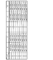
- FIG. 3 is a diagram illustrating a relationship between an index and an entry of a Log Table circuit in an arithmetic processing circuit as an example of an embodiment.
- FIG. 3 is a diagram illustrating a circuit configuration of a right shift circuit in an arithmetic processing circuit as an example of an embodiment.
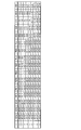
- FIG. 4 is a diagram illustrating a selector switching rule of the right shift circuit illustrated in FIG. 3.
- 6 is a flowchart for explaining an outline of processing of an arithmetic processing circuit as an example of the embodiment. 6 is a flowchart for explaining arithmetic processing in an arithmetic processing circuit as an example of the embodiment.
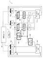
- FIG. 1 is a diagram illustrating a configuration of an arithmetic processing circuit 1 as an example of an embodiment.
- the arithmetic processing circuit (arithmetic unit) 1 is provided, for example, in a processor (arithmetic processing unit) of an information processing device and realizes arithmetic.
- the arithmetic processing circuit 1 shown in FIG. 1 is an arithmetic processing circuit that realizes two types of arithmetic operations, an exponential (EXP) arithmetic operation and a logarithmic (LOG) arithmetic operation. That is, the arithmetic processing circuit 1 selectively implements either exponential arithmetic or logarithmic arithmetic.
- a radix4 STL (Sequential Table Lookup) method for obtaining a quotient of 2 bits by one operation may be used. For example, with x as input, exp (x) is obtained. L is a variable in the power space and E is a variable in the exponential space. Further, i is the number of times the calculation is repeated.
- the STL method may be used for logarithmic calculation. For example, log (x) is obtained by inputting x.
- L is a logarithmic space variable and E is an antilogarithmic space variable. Further, i is the number of repeated calculations.
- the arithmetic processing circuit 1 shown in FIG. 1 includes registers 101 to 104, a determination circuit 105, CSAs 107 and 114, a Log Table circuit 106, right shift circuits (RSFT2) 108 and 109, and arithmetic circuits 110 to 113.
- arithmetic processing circuit 1 shown in FIG. 1 includes registers 101 to 104, a determination circuit 105, CSAs 107 and 114, a Log Table circuit 106, right shift circuits (RSFT2) 108 and 109, and arithmetic circuits 110 to 113.
- RSFT2 right shift circuits
- the register 101 may be referred to as the register LS.
- the register 102 may be referred to as a register LC
- the register 103 may be referred to as a register ES
- the register 104 may be referred to as a register EC.
- the register 101 is connected to the determination circuit 105 and the CSA 107, respectively.
- the register 101 stores the result (sum) of the Li operation performed by the CSA 107 described later. That is, the register 101 stores the mid-calculation value generated by the CSA 107 during the calculation process.
- the register value L i read from the register 101 is input to each of the determination circuit 105 and the CSA 107.
- the register 102 is connected to the determination circuit 105 and the CSA 107, respectively.
- the result (carry) of the L i calculation by the CSA 107 is stored in the register 102. That is, the register 102 stores the mid-calculation value generated by the CSA 107 during the calculation process.
- the register value L i read from the register 102 is input to each of the determination circuit 105 and the CSA 107.
- the Log Table circuit 106 and the CSA 107 realize L i operation in exponential operation or logarithmic operation.
- the right shift circuits 108 and 109, the arithmetic circuits 110 to 113, and the CSA 114 realize E i arithmetic in exponential arithmetic or logarithmic arithmetic.
- the number of bits (first number) required per cycle is reduced (for example, once). ..
- the number of bits (second number) required per cycle is increased (for example, two times or more). The second number is larger than the first number.
- n -2, -1, 0, +1, +2.
- the number of bits (first number) required per cycle is 1 when i ⁇ k
- the number of bits (second number) required per cycle is 2 when i> k.
- the determination circuit 105 selects n based on L i .
- the determination circuit 105 determines the magnitude relationship and difference between L i and 0, and selects the value of n where L i comes closest to 0.
- the determination circuit 105 selects n based on E i .
- the determination circuit 105 determines the magnitude relationship and difference between E i and 1, and selects the value of n at which E i is closest to 1.
- n determined by the determination circuit 105 is input to the arithmetic circuits 110 to 113 and the Log Table circuit 106.
- the Log Table circuit 106 outputs the value of log (1 + n * 2 ⁇ -A).
- A i
- A 2i-k.
- log (1 + n * 2 ⁇ -A) corresponding to the variables i and n is preset in the Log Table circuit 106, and the value corresponding to i and n input from the determination circuit 105 is set. Output the value of log (1 + n * 2 ⁇ -A).
- the Log Table circuit 106 has i and n as indexes and each value of log (1 + n ⁇ 2 ⁇ -i) or log (1 + n ⁇ 2 ⁇ -(2i-k)) as an entry. Have.
- FIG. 2 is a diagram illustrating a relationship between an index and an entry of the Log Table circuit 106 in the arithmetic processing circuit 1 as an example of the embodiment.
- each entry is shown in a logarithmic format with log for convenience, but in reality, each entry holds a numerical value obtained by calculating the logarithm.
- the part where “don't care” is shown is not selected.
- the Log Table circuit 106 outputs the entry values corresponding to the input i and n to the CSA 107.
- the Log Table circuit 106 stores the information in which the index and the entry are associated with each other as illustrated in FIG. 2 in a storage device (not shown), and when i and n are input, this information is input.
- the value of the corresponding entry may be acquired and output by referring to i and n as indexes.
- the Log Table circuit 106 may acquire the information illustrated in FIG. 2 from the control unit 10 or the like.
- the CSA 107 is a carry-in save adder with three inputs and two outputs (3 in-2 out), and each output is input from the registers 101 and 102 and the Log Table circuit 106. Further, of the output (calculation result) of the CSA 107, the sequence of partial sum bits is input to the register 101. On the other hand, of the output (calculation result) of the CSA 107, the carry bit string is input to the register 102.
- the CSA 107 performs a calculation of L i + 1 (L i calculation).
- the CSA 107 uses the value of log (1 + n * 2 ⁇ -A) output from the Log Table circuit 106 to calculate L i based on the above equation (3).
- the register 103 is connected to the determination circuit 105, the right shift circuit 108, and the CSA 114, respectively, and the result (sum) of the E i operation by the CSA 114 described later is stored in the register 103. That is, the register 103 stores the midway calculation value generated by the CSA 114 during the calculation process.
- the register value E i read from the register 103 is input to each of the determination circuit 105, the right shift circuit 108, and the CSA 114.
- the register 104 is connected to the determination circuit 105, the right shift circuit 109, and the CSA 114, respectively.
- the result (carry) of the E i calculation by the CSA 114 is stored in this register 104. That is, the register 104 stores the mid-calculation value generated by the CSA 114 during the calculation process.
- the register value E i read from the register 104 is input to each of the determination circuit 105, the right shift circuit 109, and the CSA 114.
- the CSA 114 is a carry-in save adder with four inputs and two outputs (4 in-2 out), and the outputs from the registers 103 and 104 and the arithmetic circuits 112 and 113 are input.
- the CSA 114 is used for exponential operation or logarithmic operation.
- the CSA 114 calculates E i + 1 .
- the CSA 114 uses the values output from the registers 103 and 104 and the arithmetic circuits 112 and 113, respectively, to calculate E i based on the above equation (3).
- the partial sum bit string of the output (calculation result) of the CSA 114 is input to the register 103.
- the carry bit string of the output (calculation result) of the CSA 114 is input to the register 104.
- the right shift circuits 108 and 109 perform a right shift on the bit string of the processing target data, and perform a number of bit shifts on the processing target data according to the number of operation repetitions i.
- the right shift circuit 108 performs a right shift operation on the register output ES of the register 103
- the right shift circuit 109 performs a right shift operation on the register output EC of the register 104 to obtain E i ⁇ 2 ⁇ -i. Or the operation of E i ⁇ 2 ⁇ -(2i-k) is realized.
- the right shift circuits 108 and 109 perform the operation of E i ⁇ 2 ⁇ -i when i ⁇ k, and the operation of E i ⁇ 2 ⁇ -(2i-k) when i> k.
- Right shift circuit 108 and 109, i only achieves calculation of E i ⁇ 2 ⁇ -i by right shifting the E i, 2i-k only E by right shifting the E i i ⁇ 2 ⁇ - ( 2i-k) is realized.
- the right shift circuits 108 and 109 have the same configuration as each other.
- FIG. 3 illustrates a circuit configuration of the right shift circuits 108 and 109 in the arithmetic processing circuit 1 as an example of the embodiment
- FIG. 4 illustrates a switching rule of the selector 1081 of the right shift circuits 108 and 109 illustrated in FIG. FIG.
- the right shift circuits 108 and 109 output the operation result of E i ⁇ 2 ⁇ -i when i ⁇ k by performing selection output by each selector 1081 according to the switching rule illustrated in FIG. 4, and i> k In the case of, the output of the operation result of E i ⁇ 2 ⁇ -(2i-k) is realized.
- D [15: 0] indicates the data to be shifted
- R [15: 0] indicates the data after the shift. Note that [15] is the sign bit. Further, i is the number of times of repeated calculation.
- the right shift circuits 108 and 109 each include a selector 1081 that receives D for each bit of R (R [0] to R [15]).
- the selector 1081 refers to the switching rule illustrated in FIG. 4 to perform selection and output according to i.
- the number of inputs to the selector 1801 is the number that i can take (9 in the example shown in FIG. 4).
- the right shift circuits 108 and 109 perform bit shift on the data to be processed by the number of times corresponding to the number of times of operation repetition i.
- the input D [15: 0] is right-shifted by i bits to become R [15: 0].
- the arithmetic circuits 110 and 111 perform a 1 ⁇ ( ⁇ 1) operation or a 2 ⁇ ( ⁇ 2) operation on the input value.
- the arithmetic circuits 110 and 111 realize a 1 ⁇ ( ⁇ 1) operation by passing the input value and a 2 ⁇ ( ⁇ 2) operation by shifting the input register value by 1 bit to the left.
- n determined by the determination circuit 105 when n determined by the determination circuit 105 is +2 or -2, the arithmetic circuits 110 and 111 perform ⁇ 2 arithmetic operation. On the other hand, when n determined by the determination circuit 105 is +1 or -1, the arithmetic circuits 110 and 111 perform x1 arithmetic operation.
- the calculation result of the calculation circuit 110 is input to the calculation circuit 112, and the calculation result of the calculation circuit 111 is input to the calculation circuit 113.
- the arithmetic circuits 112 and 113 output (through) (+) or invert (-) the input value.
- the output from the determination circuit 105 is input to the arithmetic circuits 112 and 113.
- the arithmetic circuits 112 and 113 select and set a code according to the code of n determined by the determination circuit 105.
- the control unit 10 controls the arithmetic processing in the arithmetic processing circuit 1.
- the control unit 10 operates according to an instruction from the program.
- the control unit 10 has a function as an instruction decoder, decodes the content of the instruction read in an instruction register (not shown), and controls the arithmetic processing circuit 1.
- the memory 11 is, for example, a RAM (Random Access Memory).
- the memory 11 stores, for example, initial values of the registers 101 to 104.
- the initial value is provided according to the type of arithmetic processing (exponential arithmetic and logarithmic arithmetic).
- the control unit 10 initializes the registers 101 to 104 at the start of the arithmetic processing in the arithmetic processing circuit 1.
- the control unit 10 may perform initialization by reading an initial value corresponding to the type of operation executed in the arithmetic processing circuit 1 from the memory 11 and storing it in the registers 101 to 104.
- the control unit 10 also reads out and outputs the calculation result from the registers 101 to 104 that store the result of the calculation process.
- the control unit 10 may store the information (see FIG. 2) in which the index and the entry referred to by the Log Table circuit 106 are associated with each other in the memory 11 and provide the information to the Log Table circuit 106 as appropriate.
- control unit 10 may store the switching rule (see FIG. 4) of the selector 1081 referred to by the right shift circuits 108 and 109 in the memory 11 and provide it to the right shift circuits 108 and 109 as appropriate.
- the control unit 10 may also give an instruction to start the arithmetic processing in the arithmetic processing circuit 1.
- the control unit 10 may manage i, which indicates the number of iterations (loops) of computation in the computation processing circuit 1.
- the control unit 10 may count i, and compare the value of i with a preset threshold value (imax) to determine that the loop has ended.
- step A1 the control unit 10 confirms the calculation type. If the calculation type is exponential calculation (see EXP route in step A1), the process proceeds to step A2.
- step A3 the arithmetic processing circuit 1 sets a prescribed first number (first bit number: 1 bit, for example) as the number of bits to be obtained per cycle.
- step A4 the arithmetic processing circuit 1 sets a second number (second bit number: for example, 2 bits) larger than the first number as the number of bits to be obtained per cycle.
- the right shift circuits 108 and 109 execute right shift operations according to the set number of shifts.
- step A5 the determination circuit 105 selects n based on L i .
- step A6 the exponential operation is executed with the number of bits according to the first number or the second number set in step A3 or step A4.
- step A7 the control unit 10 confirms whether the exponentiation operation is completed. If the result of this confirmation is that the exponentiation operation has not ended (see NO route in step A7), the value of i is incremented (i ++) in step A8, and the flow returns to step A2.
- step A7 when the exponential calculation is completed (see YES route in step A7), the process proceeds to step A15.
- step A15 the values of the registers 103 and 104 are output as the result of the E i calculation.
- step A1 if the result of the confirmation in step A1 is that the operation type is logarithmic operation (see the LOG route of step A1), the process proceeds to step A9.
- step A10 the arithmetic processing circuit 1 sets a prescribed first number (first bit number: 1 bit, for example) as the number of bits to be obtained per cycle.
- step A11 the arithmetic processing circuit 1 sets a second number (second bit number: for example, 2 bits) larger than the first number as the number of bits to be obtained per cycle.
- the right shift circuits 108 and 109 execute right shift operations according to the set number of shifts.
- step A12 the determination circuit 105 selects n based on E i .
- step A6 the logarithmic operation is executed with the number of bits according to the first number or the second number set in step A10 or step A11.
- step A13 the control unit 10 confirms whether the logarithmic calculation is completed. As a result of this confirmation, when the logarithmic calculation is not completed (see NO route in step A13), the value of i is incremented (i ++) in step A14, and then the process returns to step A9.
- step A13 If, as a result of the confirmation in step A13, the logarithmic calculation is completed (see YES route in step A13), the process proceeds to step A15.
- step A15 the values of the registers 101 and 102 are output as the result of the Li calculation.
- step B1 the control unit 10 confirms the type of calculation. If the calculation type is exponential calculation (see EXP route in step B1), the process proceeds to step B2.
- step B2 the registers 101 to 104 are initialized.
- the initialization of the register is performed by the control unit 10, for example.
- LS + LC L 1
- x is set in either one of LS and LC and 0 is set in the other.
- ES + EC E 1
- 1 is set to either ES or EC and 0 is set to the other.
- step B3 a loop process for repeatedly executing the control up to step B11 is started until i reaches a predetermined maximum value (imax) in the exponent calculation of the processing target.
- step B7 the determination circuit 105 determines the magnitude relationship and difference between L i and 0, and selects the value of n where L i is closest to 0.
- the Log Table circuit 106 outputs the value of log (1 + n * 2 ⁇ -A) corresponding to i and n selected by the determination circuit 105.
- step B11 loop end processing corresponding to step B3 is performed.
- i imax
- step B12 E i is output to the processing unit in the subsequent stage (for example, another arithmetic circuit or the like), and the processing ends.
- step B1 As a result of checking the operation type in step B1, if the operation type is logarithmic operation (see LOG route of step B1), the process proceeds to step B13.
- step B13 the registers 101 to 104 are initialized.
- the initialization of the register is performed by the control unit 10, for example.
- LS + LC L 1 , and for example, 0 is set for each of LS and LC.
- ES + EC E 1 , and x is set to either ES or EC and 0 is set to the other.
- step B14 a loop process for repeatedly performing the control up to step B22 is started until i reaches a predetermined maximum value (imax) in the exponent calculation of the processing target.
- step B18 the determination circuit 105 determines the magnitude relationship and difference between E i and 1, and selects the value of n at which E i is closest to 0.
- the Log Table circuit 106 outputs the value of log (1 + n * 2 ⁇ -A) corresponding to i and n selected by the determination circuit 105.
- step B22 loop end processing corresponding to step B14 is performed.
- i imax
- step B23 L i is output to the subsequent processing unit (for example, another arithmetic circuit or the like), and the process is terminated.
- the subsequent processing unit for example, another arithmetic circuit or the like
- FIG. 7 is a diagram showing a configuration example in which the arithmetic processing circuit 1 as an example of the above-described embodiment is mounted on, for example, a processor for applications such as deep learning.
- a processor for deep learning, etc. has a plurality of arithmetic units as shown in FIG. 7, and performs parallel arithmetic.
- Each arithmetic unit is provided with an EXP / LOG arithmetic unit that performs exponential arithmetic and logarithmic arithmetic, and as shown in FIG. 7, the arithmetic processing circuit 1 may be used as the EXP / LOG arithmetic unit provided in the processor.
- the processor illustrated in FIG. 7 includes an instruction unit, a plurality of register files # 1 to #m, and a plurality of execution units # 1 to #m.
- Each execution unit includes a plurality (n) of arithmetic units # 1 to #n, and the arithmetic processing circuit 1 is provided in these arithmetic units.
- the processor system illustrated in FIG. 7 has a large occupation ratio of the arithmetic units to the whole, but by applying the arithmetic processing circuit 1 to each such arithmetic unit, the effect of reducing the circuit scale of the arithmetic units can be obtained. Can be played.
- control unit 11 memory 12 processor 101-104 register 105 determination circuit 107, 114 CSA 106 Log Table circuit 108, 109 Right shift circuit 110-113 Operation circuit 1081 Selector
Landscapes
- Physics & Mathematics (AREA)
- General Physics & Mathematics (AREA)
- Engineering & Computer Science (AREA)
- Computational Mathematics (AREA)
- Mathematical Analysis (AREA)
- Pure & Applied Mathematics (AREA)
- Theoretical Computer Science (AREA)
- Computing Systems (AREA)
- Mathematical Optimization (AREA)
- General Engineering & Computer Science (AREA)
- Complex Calculations (AREA)
- Advance Control (AREA)
Abstract
L'invention concerne une unité de traitement arithmétique qui est pourvue de circuits arithmétiques 107, 114 qui effectuent des opérations exponentielles ou des opérations logarithmiques, et des unités de réglage 106, 108, 109 qui, si le nombre de répétitions de fonctionnement par un circuit arithmétique 107, 114 est inférieur ou égal à une valeur seuil, règle le nombre de bits requis par le circuit arithmétique 107, 114 pour un cycle à un premier nombre, et si le nombre de répétitions de fonctionnement est supérieur à la valeur seuil, règle le nombre de bits requis par le circuit de calcul 107, 114 pour un cycle à un second nombre supérieur au premier nombre. Ainsi, il est possible de converger au niveau d'une solution dans des opérations exponentielles ou des opérations logarithmiques sans augmenter l'échelle du circuit.
Priority Applications (2)
| Application Number | Priority Date | Filing Date | Title |
|---|---|---|---|
| JP2020554661A JP7006808B2 (ja) | 2018-10-31 | 2018-10-31 | 演算処理装置および演算処理装置の制御方法 |
| PCT/JP2018/040476 WO2020090025A1 (fr) | 2018-10-31 | 2018-10-31 | Unité de traitement arithmétique et procédé de commande d'unité de traitement arithmétique |
Applications Claiming Priority (1)
| Application Number | Priority Date | Filing Date | Title |
|---|---|---|---|
| PCT/JP2018/040476 WO2020090025A1 (fr) | 2018-10-31 | 2018-10-31 | Unité de traitement arithmétique et procédé de commande d'unité de traitement arithmétique |
Publications (1)
| Publication Number | Publication Date |
|---|---|
| WO2020090025A1 true WO2020090025A1 (fr) | 2020-05-07 |
Family
ID=70462894
Family Applications (1)
| Application Number | Title | Priority Date | Filing Date |
|---|---|---|---|
| PCT/JP2018/040476 Ceased WO2020090025A1 (fr) | 2018-10-31 | 2018-10-31 | Unité de traitement arithmétique et procédé de commande d'unité de traitement arithmétique |
Country Status (2)
| Country | Link |
|---|---|
| JP (1) | JP7006808B2 (fr) |
| WO (1) | WO2020090025A1 (fr) |
Cited By (1)
| Publication number | Priority date | Publication date | Assignee | Title |
|---|---|---|---|---|
| US20210365239A1 (en) * | 2020-05-25 | 2021-11-25 | Realtek Semiconductor Corp. | Logarithm calculation method and logarithm calculation circuit |
Citations (3)
| Publication number | Priority date | Publication date | Assignee | Title |
|---|---|---|---|---|
| JPH02118725A (ja) * | 1988-10-28 | 1990-05-07 | Nec Corp | 対数関数演算装置 |
| JPH0934693A (ja) * | 1995-07-21 | 1997-02-07 | Nec Corp | 指数対数変換回路 |
| JP2009276990A (ja) * | 2008-05-14 | 2009-11-26 | Sharp Corp | 演算装置およびその演算方法、信号処理装置、演算装置制御プログラム、並びに該プログラムを記録した記録媒体 |
-
2018
- 2018-10-31 JP JP2020554661A patent/JP7006808B2/ja active Active
- 2018-10-31 WO PCT/JP2018/040476 patent/WO2020090025A1/fr not_active Ceased
Patent Citations (3)
| Publication number | Priority date | Publication date | Assignee | Title |
|---|---|---|---|---|
| JPH02118725A (ja) * | 1988-10-28 | 1990-05-07 | Nec Corp | 対数関数演算装置 |
| JPH0934693A (ja) * | 1995-07-21 | 1997-02-07 | Nec Corp | 指数対数変換回路 |
| JP2009276990A (ja) * | 2008-05-14 | 2009-11-26 | Sharp Corp | 演算装置およびその演算方法、信号処理装置、演算装置制御プログラム、並びに該プログラムを記録した記録媒体 |
Cited By (1)
| Publication number | Priority date | Publication date | Assignee | Title |
|---|---|---|---|---|
| US20210365239A1 (en) * | 2020-05-25 | 2021-11-25 | Realtek Semiconductor Corp. | Logarithm calculation method and logarithm calculation circuit |
Also Published As
| Publication number | Publication date |
|---|---|
| JPWO2020090025A1 (ja) | 2021-09-24 |
| JP7006808B2 (ja) | 2022-01-24 |
Similar Documents
| Publication | Publication Date | Title |
|---|---|---|
| JP6694880B2 (ja) | 有効度整合 | |
| JP6540725B2 (ja) | 演算処理装置、方法、およびプログラム | |
| US8271571B2 (en) | Microprocessor | |
| US20230333815A1 (en) | Concurrent multi-bit adder | |
| JP7096828B2 (ja) | 入力オペランド値を処理するための装置及び方法 | |
| JPH1078863A (ja) | 浮動小数点式ハードウェアを用いたマイクロプロセッサ整数除法演算を実行するための方法および装置 | |
| WO2013109532A1 (fr) | Processeur algébrique | |
| KR100744216B1 (ko) | 계산 장치 및 방법과 컴퓨터 프로그램 저장 매체 | |
| JP6877812B2 (ja) | 重複伝搬演算 | |
| JP7006808B2 (ja) | 演算処理装置および演算処理装置の制御方法 | |
| US20250362874A1 (en) | Systems and methods for shift last multiplication and accumulation (mac) process | |
| TWI235328B (en) | Logic network and methods of computing | |
| US9612800B2 (en) | Implementing a square root operation in a computer system | |
| US7016927B2 (en) | Method and apparatus for modular multiplication | |
| US9703525B2 (en) | Partially and fully parallel normaliser | |
| Maxfield | An introduction to different rounding algorithms | |
| JP2024508596A5 (fr) | ||
| CN115079997A (zh) | 对数执行硬件高效无偏舍入的方法 | |
| KR100900790B1 (ko) | 재구성형 프로세서 연산 방법 및 장치 | |
| US7139786B2 (en) | Method and apparatus for efficiently performing a square root operation | |
| CN116149600B (zh) | 多常数乘法器的逻辑电路设置方法、装置、设备及介质 | |
| TWI229802B (en) | Emod a fast modulus calculation for computer systems | |
| JP7120320B2 (ja) | 演算処理装置および演算処理装置の制御方法 | |
| JPH10333883A (ja) | 乗算方法および乗算回路 | |
| JPWO2020090024A1 (ja) | 演算処理装置 |
Legal Events
| Date | Code | Title | Description |
|---|---|---|---|
| 121 | Ep: the epo has been informed by wipo that ep was designated in this application |
Ref document number: 18938969 Country of ref document: EP Kind code of ref document: A1 |
|
| ENP | Entry into the national phase |
Ref document number: 2020554661 Country of ref document: JP Kind code of ref document: A |
|
| NENP | Non-entry into the national phase |
Ref country code: DE |
|
| 122 | Ep: pct application non-entry in european phase |
Ref document number: 18938969 Country of ref document: EP Kind code of ref document: A1 |