WO2020090601A1 - Substrat de câblage d'encapsulation de semi-conducteur et procédé de fabrication de substrat de câblage d'encapsulation de semi-conducteur - Google Patents
Substrat de câblage d'encapsulation de semi-conducteur et procédé de fabrication de substrat de câblage d'encapsulation de semi-conducteur Download PDFInfo
- Publication number
- WO2020090601A1 WO2020090601A1 PCT/JP2019/041634 JP2019041634W WO2020090601A1 WO 2020090601 A1 WO2020090601 A1 WO 2020090601A1 JP 2019041634 W JP2019041634 W JP 2019041634W WO 2020090601 A1 WO2020090601 A1 WO 2020090601A1
- Authority
- WO
- WIPO (PCT)
- Prior art keywords
- wiring board
- wiring
- layer
- semiconductor chip
- interposer
- Prior art date
- Legal status (The legal status is an assumption and is not a legal conclusion. Google has not performed a legal analysis and makes no representation as to the accuracy of the status listed.)
- Ceased
Links
Images








Classifications
-
- H—ELECTRICITY
- H05—ELECTRIC TECHNIQUES NOT OTHERWISE PROVIDED FOR
- H05K—PRINTED CIRCUITS; CASINGS OR CONSTRUCTIONAL DETAILS OF ELECTRIC APPARATUS; MANUFACTURE OF ASSEMBLAGES OF ELECTRICAL COMPONENTS
- H05K3/00—Apparatus or processes for manufacturing printed circuits
- H05K3/46—Manufacturing multilayer circuits
-
- H—ELECTRICITY
- H10—SEMICONDUCTOR DEVICES; ELECTRIC SOLID-STATE DEVICES NOT OTHERWISE PROVIDED FOR
- H10W—GENERIC PACKAGES, INTERCONNECTIONS, CONNECTORS OR OTHER CONSTRUCTIONAL DETAILS OF DEVICES COVERED BY CLASS H10
- H10W70/00—Package substrates; Interposers; Redistribution layers [RDL]
- H10W70/60—Insulating or insulated package substrates; Interposers; Redistribution layers
-
- H—ELECTRICITY
- H10—SEMICONDUCTOR DEVICES; ELECTRIC SOLID-STATE DEVICES NOT OTHERWISE PROVIDED FOR
- H10W—GENERIC PACKAGES, INTERCONNECTIONS, CONNECTORS OR OTHER CONSTRUCTIONAL DETAILS OF DEVICES COVERED BY CLASS H10
- H10W78/00—Detachable holders for supporting packaged chips in operation
-
- H—ELECTRICITY
- H10—SEMICONDUCTOR DEVICES; ELECTRIC SOLID-STATE DEVICES NOT OTHERWISE PROVIDED FOR
- H10W—GENERIC PACKAGES, INTERCONNECTIONS, CONNECTORS OR OTHER CONSTRUCTIONAL DETAILS OF DEVICES COVERED BY CLASS H10
- H10W74/00—Encapsulations, e.g. protective coatings
- H10W74/10—Encapsulations, e.g. protective coatings characterised by their shape or disposition
- H10W74/15—Encapsulations, e.g. protective coatings characterised by their shape or disposition on active surfaces of flip-chip devices, e.g. underfills
-
- H—ELECTRICITY
- H10—SEMICONDUCTOR DEVICES; ELECTRIC SOLID-STATE DEVICES NOT OTHERWISE PROVIDED FOR
- H10W—GENERIC PACKAGES, INTERCONNECTIONS, CONNECTORS OR OTHER CONSTRUCTIONAL DETAILS OF DEVICES COVERED BY CLASS H10
- H10W90/00—Package configurations
- H10W90/701—Package configurations characterised by the relative positions of pads or connectors relative to package parts
- H10W90/721—Package configurations characterised by the relative positions of pads or connectors relative to package parts of bump connectors
- H10W90/724—Package configurations characterised by the relative positions of pads or connectors relative to package parts of bump connectors between a chip and a stacked insulating package substrate, interposer or RDL
-
- H—ELECTRICITY
- H10—SEMICONDUCTOR DEVICES; ELECTRIC SOLID-STATE DEVICES NOT OTHERWISE PROVIDED FOR
- H10W—GENERIC PACKAGES, INTERCONNECTIONS, CONNECTORS OR OTHER CONSTRUCTIONAL DETAILS OF DEVICES COVERED BY CLASS H10
- H10W90/00—Package configurations
- H10W90/701—Package configurations characterised by the relative positions of pads or connectors relative to package parts
- H10W90/731—Package configurations characterised by the relative positions of pads or connectors relative to package parts of die-attach connectors
- H10W90/734—Package configurations characterised by the relative positions of pads or connectors relative to package parts of die-attach connectors between a chip and a stacked insulating package substrate, interposer or RDL
Definitions
- the present invention relates to a wiring board for a semiconductor package and a manufacturing method thereof.
- connection between the FC-BGA wiring board and the motherboard requires connection with a connection terminal having a wide pitch that is almost the same as the conventional one.
- Patent Document 1 discloses a technique for connecting a wiring board to an FC-BGA wiring board.
- Patent Document 2 discloses a technique of forming fine wiring by flattening the surface of an FC-BGA wiring substrate by chemical mechanical polishing (CMP) or the like.
- the silicon interposer When using a silicon interposer, it is excellent in forming fine wiring because the flatness of the substrate surface is good.
- the silicon interposer is manufactured by using a silicon wafer and using equipment for a pre-process of a semiconductor manufacturing process, a problem of high cost is pointed out. Specifically, since the silicon wafer has shape and size restrictions, the number of interposers that can be manufactured from a single wafer is suppressed, and the manufacturing equipment is also expensive. Therefore, the manufacturing cost of the silicon interposer is generally low. Become higher. Further, since the silicon wafer is a semiconductor, there is also a problem that the transmission characteristics are deteriorated.
- Patent Document 2 the technique of flattening the wiring board for FC-BGA and forming a fine wiring layer thereon can avoid the problem of transmission characteristic deterioration.
- the yield in the highly difficult fine wiring layer forming step is relatively low, and therefore the total yield resulting from the multiplication is extremely poor.
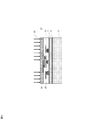
- a semiconductor chip bonding portion 31 such as a copper pillar is formed on the wiring board for FC-BGA by a protruding electrode made of solder 30. Since the solder 30 spreads in the direction parallel to the surface of the FC-BGA wiring board when joining, there is a problem that the connection area between the semiconductor chip joining portion 31 such as a copper pillar and the solder 30 is reduced. Further, the solder 30 may spread in the parallel direction to come into contact with the solder of the adjacent semiconductor chip joint portion 31, or even if there is no contact, a short circuit may occur due to ion migration.
- the interposer on the semiconductor chip mounting side it is necessary for the interposer on the semiconductor chip mounting side to support narrow pitch chip mounting of 55 ⁇ m pitch. Since thermal compression bonding (TCB) is used in the narrow pitch chip mounting, the solder on the copper pillar spreads in the direction parallel to the surface of the FC-BGA wiring board due to heat and pressure (see Fig. 6), etc. If the copper pillar or the like comes into contact with the connecting portion and short-circuits, the yield may be significantly reduced.
- TAB thermal compression bonding
- the present invention has been made in view of the above problems, and is for a semiconductor package that suppresses a decrease in the yield of the semiconductor package, can satisfactorily mount a semiconductor chip, and has high connection reliability.
- An object of the present invention is to provide a wiring board and a manufacturing method thereof.
- a wiring board for a semiconductor package in which a second wiring board including a buildup layer having an insulating resin layer and a wiring layer is joined to a first wiring board,
- the thickness of the second wiring board is 10 ⁇ m to 1000 ⁇ m
- the first wiring board and the second wiring board are electrically connected via a protruding electrode formed on a pad provided on the side of the first wiring board of the second wiring board, and between the two.
- On a surface of the second wiring board opposite to the first wiring board a semiconductor chip connection pad for connecting to a semiconductor chip and an insulating resin are provided.
- the semiconductor chip connection pad is a laminated body made of a metal material having a gold layer on the outermost surface, and the outermost surface is exposed in a recess formed on the surface of the insulating resin.
- a wiring board for a semiconductor package which can suppress a decrease in the yield of the semiconductor package, can satisfactorily mount a semiconductor chip, and have high connection reliability, and a manufacturing method thereof. Will be possible.
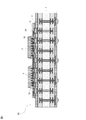
- FIG. 1 is a sectional view showing an example in which a semiconductor chip is mounted on a semiconductor package wiring board according to an embodiment of the present invention.
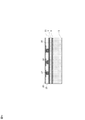
- FIG. 2 is a cross-sectional view showing, in an enlarged manner, a part of a connection portion between a wiring board in which a semiconductor chip is mounted on a wiring board for a semiconductor package according to an embodiment of the present invention and the semiconductor chip.
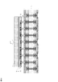
- FIG. 3A is a cross-sectional view showing an example of an interposer formed on a carrier substrate according to an embodiment of the present invention.
- FIG. 3B is a partially enlarged view of FIG. 3A.
- FIG. 4 shows that an interposer with a carrier substrate according to an embodiment of the present invention is joined to an FC-BGA wiring substrate, an interposer underfill is filled and cured in a gap formed by joining the two, and then the carrier substrate is interposer.
- FIG. 5A is a sectional view illustrating a series of manufacturing steps for a wiring board according to an embodiment of the present invention.
- FIG. 5B is a sectional view illustrating a series of manufacturing steps for the wiring board according to the embodiment of the present invention.
- FIG. 5C is a sectional view illustrating a series of manufacturing steps for the wiring board according to the embodiment of the present invention.
- FIG. 5D is a sectional view illustrating a series of manufacturing steps for the wiring board according to the embodiment of the present invention.
- FIG. 5E is a sectional view illustrating a series of manufacturing steps for the wiring board according to the embodiment of the present invention.
- FIG. 5F is a sectional view illustrating a series of manufacturing steps for the wiring board according to the embodiment of the present invention.
- FIG. 5G is a sectional view illustrating a series of manufacturing steps for the wiring board according to the embodiment of the present invention.
- FIG. 5H is a sectional view illustrating a series of manufacturing steps for the wiring board according to the embodiment of the present invention.
- FIG. 5I is a sectional view illustrating a series of manufacturing steps for the wiring board according to the embodiment of the present invention.
- FIG. 5J is a sectional view illustrating a series of manufacturing steps for the wiring board according to the embodiment of the present invention.
- FIG. 5K is a sectional view illustrating a series of manufacturing steps for the wiring board according to the embodiment of the present invention.
- FIG. 5L is a sectional view illustrating a series of manufacturing steps for the wiring board according to the embodiment of the present invention.
- FIG. 5M is a sectional view illustrating a series of manufacturing steps for the wiring board according to the embodiment of the present invention.
- FIG. 5N is a sectional view illustrating a series of manufacturing steps for a wiring board according to an embodiment of the present invention.
- FIG. 5O is a sectional view illustrating a series of manufacturing steps for the wiring board according to the embodiment of the present invention.
- FIG. 5P is a sectional view illustrating a series of manufacturing steps for the wiring board according to the embodiment of the present invention.
- FIG. 5Q is a sectional view illustrating a series of manufacturing steps for the wiring board according to the embodiment of the present invention.
- FIG. 5R is a sectional view illustrating a series of manufacturing steps for the wiring board according to the embodiment of the present invention.
- FIG. 5S is a sectional view illustrating a series of manufacturing steps for the wiring board according to the embodiment of the present invention.
- FIG. 5T is a sectional view illustrating a series of manufacturing steps for the wiring board according to the embodiment of the present invention.
- FIG. 6 is an enlarged cross-sectional view showing a part of a connection portion between a wiring board for mounting a semiconductor chip on a wiring board for a semiconductor package and a semiconductor chip according to a conventional embodiment.
- a wiring board according to an embodiment of the present invention will be described below with reference to the drawings.
- portions corresponding to each other are designated by the same reference numerals, and description of overlapping portions will be appropriately omitted.
- each drawing may be exaggerated as appropriate for ease of explanation.
- one embodiment of the present invention exemplifies a configuration for embodying the technical idea of the present invention, and does not specify the material, shape, structure, arrangement, etc. of each part as follows. ..
- the technical idea of the present invention can be appropriately modified within the technical scope defined by the claims described in the claims.
- FIG. 1 is a sectional view showing an example of a semiconductor package 50 in which a semiconductor chip 4 is mounted on a semiconductor package wiring board 100.
- a semiconductor package 50 according to an embodiment of the present invention is a build-up wiring layer in which a resin layer and a wiring layer are alternately laminated on one surface of an FC-BGA wiring substrate (also referred to as a first wiring substrate) 1.
- An interposer underfill 2 which is an adhesive made of an insulating resin, is filled in the gap between the FC-BGA wiring board 1 and the interposer 3 and is cured.
- the semiconductor chip 4 is bonded to the surface of the interposer 3 opposite to the FC-BGA wiring substrate 1 via the semiconductor chip bonding portion 31 made of a copper pillar or the like, and in the gap between the semiconductor chip 4 and the interposer 3. Is filled and cured with an underfill 32 for a semiconductor chip, which is an adhesive made of an insulating resin.
- the semiconductor chip connection pad 14 is provided with an Au (gold) layer on its surface and is provided on the peripheral surface of the insulating resin 15.
- the interposer 3 side of the semiconductor package wiring substrate 100 is connected via a copper pillar, a copper post, or the like, which is the semiconductor chip bonding portion 31 of the semiconductor chip 4. Further, by filling the gap between the semiconductor chip connecting pad 14 and the semiconductor chip 4 with the underfill 32 and curing the same, the semiconductor package 50 as shown in FIG. 1 can be obtained.
- the underfill 2 is an adhesive material used to fix and seal the FC-BGA wiring board 1 and the interposer 3.
- the underfill 2 for example, epoxy resin, urethane resin, silicon resin, polyester resin, oxetane resin, and maleimide resin, or a resin in which two or more kinds of these resins are mixed, silica as a filler, oxidation A material to which titanium, aluminum oxide, magnesium oxide, zinc oxide, or the like is added is used.
- the underfill 2 may be formed by filling a liquid resin.
- the wiring board for FC-BGA 1 And the interposer 3 may be fixed and these gaps may be sealed.
- the underfill 32 is an adhesive used to fix and seal the semiconductor chip 4 and the interposer 3, and is made of the same material as the underfill 2.
- the anisotropic conductive film (ACF) or the film-like connecting material (NCF) may be used instead of the underfill 32.
- the wiring pitch of the portion of the interposer 3 that is joined to the semiconductor chip 4 is joined to the semiconductor chip 4 of the FC-BGA wiring substrate 1 when the semiconductor chip 4 and the FC-BGA wiring substrate 1 are directly joined. It is narrower than the part wiring pitch. That is, the wiring pitch on the surface of the interposer 3 on which the semiconductor chip 4 is mounted is finer than the wiring pitch of the FC-BGA wiring board 1 when the semiconductor chip 4 is directly bonded to the FC-BGA wiring board 1. Has become.
- (Semiconductor chip joint) 2 and 5T are enlarged sectional views showing an example of a joint between the semiconductor package wiring board 100 in which the semiconductor chip 4 is mounted on the semiconductor package wiring board 100 according to the present embodiment in FIG. 1 and the semiconductor chip 4. It is a figure.
- the pad portion (semiconductor chip connecting pad 14) bonded to the semiconductor chip 4 is within the recess of the insulating resin 15 within a range (depth d) of 0.3 ⁇ m or more and 5.0 ⁇ m or less, and the insulating resin around the recess. It is exposed at a position recessed from 15.
- the solder creeps up on the semiconductor chip joint portion 31 such as the copper pillar or the copper post, and the solder is covered and protected by the solder.
- the solder creeps up on the semiconductor chip joint portion 31, the semiconductor chip joint portion 31 is protected by the solder, and the contact area increases, so that the connection reliability is improved.
- the interposer 3 in order to comply with the current high-band memory (HBM) specifications, it is necessary for the interposer 3 to have a wiring width of 2 ⁇ m or more and 6 ⁇ m or less. In order to adjust the characteristic impedance to 50 ⁇ , if the wiring width is 2 ⁇ m and the wiring height is 2 ⁇ m, the insulation film thickness between the wiring is 2.5 ⁇ m, and the thickness of one layer including the wiring is 4.5 ⁇ m. .. When forming the 5-layer interposer 3 with this thickness, the interposer 3 is a very thin interposer having a total thickness of about 25 ⁇ m.
- FIG. 3A is a cross-sectional view illustrating a state in which an interposer is formed on the carrier substrate 5.
- FIG. 3B is a cross-sectional view enlarging and illustrating a part of FIG. 3A.
- the thin wiring layer 3a which is the interposer 3 is formed in a later step.
- the release layer 6 for separating from the carrier substrate 5 is formed on the carrier substrate 5 to form an interposer with a carrier substrate.
- the carrier substrate 5 a glass substrate having a surface flatness equivalent to that of a silicon wafer and a small thermal expansion coefficient can be preferably used, but the carrier substrate 5 is not limited to the glass substrate.
- the thin interposer 3 is less affected by temperature changes because the stress due to the difference in coefficient of thermal expansion (CTE: Coefficient of Thermal Expansion) is small. Therefore, the influence of the CTE difference between the FC-BGA wiring board 1 and the semiconductor chip 4 can be reduced, and the connection reliability can be improved.
- CTE Coefficient of Thermal Expansion
- the thickness of the interposer 3 is preferably 10 ⁇ m or more and 100 ⁇ m or less (preferably 20 ⁇ m or more and 50 ⁇ m or less), but if it is 1000 ⁇ m or less, the thinning effect of the semiconductor package wiring board 100 can be exhibited. In particular, the maximum effect can be exhibited when the thickness is about 10 ⁇ m to 20 ⁇ m.
- a thin interposer 3 having a thickness of 10 ⁇ m or more and 1000 ⁇ m or less can be formed for FC-BGA.
- the wiring board 1 can be flatly bonded.
- the wiring board for FC-BGA has high rigidity, and when the CTE difference with the semiconductor chip is large, the joint portion is easily broken in an environment where the temperature changes drastically such as in a heat cycle test. However, even under the same conditions, if the height of the joint is high, the joint is less likely to be broken.
- the FC-BGA wiring board 1 and the semiconductor chip 4 are joined via the thin interposer 3. Therefore, the interposer 3 serves as a buffer layer, and the CTE difference between the interposers 3 is unlikely to influence, so that high reliability can be secured.
- a glass substrate can be used as the carrier substrate 5.
- the glass substrate has excellent flatness and is suitable for forming a fine pattern on the wiring layer 3a. Further, since the glass substrate has a small CTE and is less likely to be distorted, it has excellent pattern position accuracy and flatness when bonded to the FC-BGA wiring substrate 1.
- the thickness of the glass substrate is preferably thick from the viewpoint of suppressing the occurrence of warpage in the manufacturing process, and for example, a thickness of 0.7 mm or more and 1.1 mm or less is desirable. .. Further, the usable glass substrate has a CTE of 3 ppm / ° C. or more and 15 ppm / ° C. or less, and it is particularly preferable to use a glass substrate of about 9 ppm / ° C. from the viewpoint of the CTE difference between the FC-BGA wiring substrate and the semiconductor chip. ..
- the carrier substrate 5 not an expensive silicon substrate, but a substrate such as a glass substrate which is inexpensive and has flatness equivalent to that of a silicon substrate can be used, so that the cost can be reduced.
- a wiring board to be the interposer 3 is manufactured.
- a peeling layer 6 that allows the interposer 3 to be peeled from the carrier substrate 5 is formed on one surface of the carrier substrate 5 in a later step.
- the wiring protection layer 7 is a layer for protecting the wiring layer 3a when it is peeled from the carrier substrate 5 in a later step.
- the wiring protection layer 7 is any one selected from an epoxy resin, an acrylic resin, a urethane resin, a silicon resin, a polyester resin, and an oxetane resin, or a resin in which two or more kinds selected from these resins are mixed. Any resin that can be removed after the carrier substrate 5 is peeled off may be used.
- the method for forming the wiring protection layer 7 may be appropriately selected according to the form of the resin, such as spin coating and laminating. For example, a film-shaped acrylic resin can be formed by a laminating method.
- a carrier seed layer 11 is formed on the wiring protection layer 7.
- the carrier seed layer 11 can be formed using a thin film forming technique such as a sputtering method or a vacuum deposition method.
- a thin film forming technique such as a sputtering method or a vacuum deposition method.
- the layers can be laminated in order, but the configuration and thickness may be appropriately set depending on the application.
- Ti: 50 nm and Cu: 300 nm can be stacked.
- a resist pattern 13 is formed on the carrier seed layer 11, and a semiconductor chip connection pad 14 for connection with the semiconductor chip 4 is formed in the opening 13a by electrolytic plating.
- electrolytic plating electrolytic copper plating can be preferably used, but the electrolytic plating is not limited to this.
- the wiring layer 3a to be the interposer 3 is bonded to the FC-BGA wiring substrate 1, and then the carrier substrate 5 is peeled off. After peeling the carrier substrate 5, the wiring protection layer 7 and the carrier seed layer 11 are removed to expose the semiconductor chip connection pads 14.
- the nickel layer, the gold layer, the nickel layer, the copper layer (Ni / Au / Ni / Cu) or the nickel layer is formed so that the surface of the semiconductor chip connection pad 14 becomes Au (gold).
- a layer, a gold layer, a lead layer, a nickel layer, and copper plating (Ni / Au / Pd / Ni / copper plating) are laminated in this order.
- the nickel layer is referred to as a material layer, and the other layers are referred to as metal layers. It is preferable to form Ni plating on the carrier seed layer 11 with a film thickness of 0.3 ⁇ m or more and 5.0 ⁇ m or less. By doing so, after removing the carrier substrate 5, the Ni plating is removed to form a recessed pad portion which is a recess having the insulating resin 15 as a partition in the range of 0.3 ⁇ m or more and 5.0 ⁇ m or less. be able to.
- the insulating resin 15 is formed.
- the insulating resin 15 is formed so that the semiconductor chip connecting pad 14 is embedded in the layer of the insulating resin 15.
- the insulating resin 15 is formed by a spin coating method using an epoxy resin which is a photosensitive insulating resin.
- the photosensitive epoxy resin can be cured at a relatively low temperature, and the shrinkage due to the curing (curing) after formation of the conductive via after that is small, and the step can be suppressed, and it is excellent for the subsequent fine pattern formation. There is.
- the insulating resin 15 may be formed by spin coating using a photosensitive epoxy resin, or may be formed by compression curing an insulating resin film with a vacuum laminator, and in this case, flatness is good.
- the insulating film can be formed.
- Polyimide may be used as the insulating resin as long as a slight level difference can be allowed in the exposure step.
- the conductive via 17 and the wiring 21 are formed toward the semiconductor chip connecting pad 14.
- a photosensitive epoxy resin is used for the insulating resin 15, and the removal pattern of the photosensitive epoxy resin for forming the conductive via 17 and the wiring 21 by performing UV exposure 25 (FIG. 5G) and development. Are formed (FIG. 5H).
- a vacuum deposition apparatus such as a sputtering apparatus, an ion plating apparatus, or a vacuum deposition apparatus was used.
- a film device is used to continuously form Ti and Cu to form a seed layer 18 for electrolytic plating.
- electrolytic copper plating is performed to form a copper plating film 20 on the seed layer 18.
- the copper plating film 20 is polished by CMP or surface polishing until the insulating resin 15 is exposed, and the wiring 21 connected to the conductive via 17 is formed.
- the conductive via 17 may be formed by laser light irradiation and the wiring 21 may be formed using a resist pattern.
- the build-up wiring layer can be formed by repeating the wiring layer forming step shown in FIGS. 5F to 5J in accordance with the number of stacked wiring layers by using the steps described above as the wiring forming step.
- the build-up wiring layers are sequentially formed on the carrier substrate 5, one wiring 21 and the conductive via 17 in the wiring layer 3a are combined with each other in the manufacturing process, and thus the wiring board for FC-BGA is combined.
- the cross-sectional shape increases as it approaches 1 (away from the underfill 32), and the conductive via 17 has a tapered tip shape, for example.
- the conductive via 17 has a taper shape which becomes tapered as the conductive via 17 moves away from the underfill 32 (closer to the FC-BGA wiring substrate (not shown)) in the manufacturing process. It can be distinguished from the interposer 3 of the form.
- a wiring layer including a pad 27 on the interposer side that is connected to the FC-BGA wiring substrate via a protruding electrode such as a solder ball is formed.
- a solder resist layer 16 made of a heat-resistant insulating resin is formed on the outermost surface of the interposer 3 on the FC-BGA wiring substrate 1 side. As shown in FIG. 5K, the solder resist layer 16 is formed so as to cover the region including the pad 27 and the insulating resin 15.
- UV exposure 25 is performed to form the opening 16a (see FIG. 5M) at the portion where the pad 27 is exposed.
- the solder resist layer 16 is cured and stabilized by baking.
- the opening (recess) 16a is formed by developing the solder resist layer 16.
- surface treatment is performed to prevent copper from being oxidized on the surface of the pad 27 and to improve the wettability of the solder bump.
- a pad surface treatment layer 23 is formed on the surface of the pad 27 by laminating a nickel layer, a lead layer, and a gold layer (Ni / Pd / Au) in this order.
- An OSP (Organic Soilerability Preservative, surface treatment with water-soluble preflux) film may be formed on the surface of the pad 27. Further, it may be appropriately selected from electroless tin plating, nickel layer and gold layer (Ni / Au) depending on the application.
- the solder bumps 24 are formed by reflow or the like, and then the carrier substrate 5 is divided into individual pieces, whereby the interposer with the carrier substrate 5 is formed. 3 can be obtained.
- the terminals of the interposer 3 with a carrier substrate that is, the FC-BGA wiring substrate 1 designed and manufactured according to the positions of the solder bumps 24 and the interposer 3 with a carrier substrate are aligned. ..
- the FC-BGA wiring substrate 1 and the interposer 3 with the carrier substrate are joined by flip-chip mounting.
- the underfill 2 is filled in the gap formed between the interposer 3 and the FC-BGA wiring substrate 1 and is fixed by curing.
- the wiring board 1 for FC-BGA and the wiring layer 3a formed on the carrier substrate 5 to be the interposer 3 are manufactured separately, and these are bonded to each other, whereby the wiring board for the semiconductor package is manufactured. 100 has been achieved. Therefore, when the FC-BGA wiring board 1 and the wiring layer 3a (interposer 3) provided with the carrier substrate 5 are bonded together, only good products of each are selected, and the good products are bonded together to form the semiconductor package wiring board 100. To make. As a result, it is possible to achieve a high production yield and to efficiently produce the semiconductor package wiring substrate 100 without manufacturing the semiconductor package wiring substrate 100 in which either one is defective or both are defective. Is possible.
- the FC-BGA wiring board 1 and the wiring layer 3a provided with the carrier substrate 5 are joined after the respective manufacturing processes are completed, the wiring density, the number of layers, and the structure of the front and back surfaces of the substrate can be reduced. It is possible to prevent the semiconductor package wiring substrate 100 from being warped due to the difference. Furthermore, since the carrier substrate 5 is made of a material having high rigidity and low CTE and little distortion, the surface of the wiring layer 3a after the carrier substrate 5 is removed is flat, and the semiconductor chip connection pads 14 are The positional accuracy is also improved, and the semiconductor chip 4 can be easily mounted.
- the carrier substrate 5 and the peeling layer 6 are peeled together from the interposer 3.
- the wiring protection layer 7 remaining on the surface of the interposer 3 is removed.
- an alkali-soluble resin used for the wiring protection layer 7, it can be removed with an alkaline solvent (1% NaOH, 2.3% TMAH).
- the Ni plating film on the surface of the interposer 3 is removed by etching (at the same time, the nickel layer overlying the semiconductor chip connecting pad 14 is removed), and the semiconductor chip for connecting to the semiconductor chip 4 is removed.
- the Au film of the connection pad 14 is exposed.
- the wiring board 100 for semiconductor packages which is a wiring board for FC-BGA with an extremely thin interposer, is completed.
- the semiconductor chip connection pads 14 are provided in the recesses of the insulating resin 15 and are 0.3 ⁇ m or more and 5.0 ⁇ m or less from the surface. It is low in the range. That is, a structure is formed in which the insulating resin 15 serves as a partition and surrounds the semiconductor chip connecting pad 14. Therefore, the solder 30 does not spread in the direction parallel to the plane of the interposer 3 and creeps up to the semiconductor chip bonding portion 31. Therefore, it is possible to prevent the problem that the solder 30 reaches the adjacent semiconductor chip connection pads 14 and short-circuits.
- the semiconductor chip joints 31 such as the copper pillars and the copper posts are protected by the solder and also have the effect of increasing the connection area, they have a high reliability and an effect of improving the production yield. ..
- the FC-BGA wiring board 1 and the semiconductor chip 4 are bonded to each other via the interposer 3, so that the bonding distance (FC-BGA wiring board 1 and semiconductor Since the distance between the facing surfaces of the chip 4 is increased, the influence of the CTE difference can be mitigated.
- the carrier substrate 5 may be made of a metal material having a flatness with little distortion, or a ceramic substrate.
- a ceramic substrate it is easy to adjust the CTE to a desired value, and the CTE can be changed according to the constituent material of the interposer 3.
- the wiring layer 3a (interposer 3) with the carrier substrate 5 is used for FC-BGA by using a foaming resin layer that foams by heating as the peeling layer 6, for example.
- the carrier substrate 5 may be peeled from the wiring layer 3a by heating and foaming the expandable resin layer.
- the thickness of the interposer including the build-up wiring layer flip-chip mounted on the wiring board for FC-BGA via the protruding electrode is 10 ⁇ m to 1000 ⁇ m, which is very thin.
- the influence of the thermal stress due to the CTE difference of the BGA wiring board on the semiconductor package wiring board is reduced. Therefore, deformation such as warpage of the semiconductor package wiring board is small, and the semiconductor chip can be easily mounted.
- the semiconductor chip connecting pad provided in the interposer of the present embodiment is provided in the recessed portion that is recessed in the range of 0.3 ⁇ m or more and 5 ⁇ m or less from the surface of the insulating resin around the pad.
- the copper pillar is protected by the solder crawling up to the copper pillar that is the semiconductor chip joint portion 31, increasing the connection area, and in the direction parallel to the surface of the FC-BGA wiring board 1. It is possible to prevent the solder from spreading. Therefore, high reliability and high production yield can be obtained.
- the interposer is interposed between the semiconductor chip and the FC-BGA wiring board, so the distance between the two becomes large. Therefore, the stress generated between the semiconductor chip and the FC-BGA wiring board due to the CTE difference is relaxed, so that a semiconductor package having high connection reliability can be provided.
- a highly flat and rigid substrate such as a glass substrate is used as a carrier substrate, and a build-up wiring layer is formed on the carrier substrate. Since the interposer is manufactured and then flip-chip mounted on the FC-BGA wiring board, it is possible to manufacture a semiconductor package wiring board having a thin interposer having a thickness of 10 ⁇ m to 1000 ⁇ m.
- the wiring board for a semiconductor package is manufactured by manufacturing the interposer with a carrier board and the wiring board for FC-BGA in separate steps and flip-mounting them. Therefore, it becomes possible to select only non-defective products for both and to perform flip-chip mounting. Therefore, the yield of the flip-chip mounting process can be increased.
- the Au layer on the outermost surface is recessed within a range of 0.3 ⁇ m or more and 5.0 ⁇ m or less from the surface of the surrounding insulating resin. Since the pad is a recessed pad, it is possible to prevent molten solder from creeping up to a semiconductor chip bonding portion such as a copper post of a semiconductor chip when the chip is flip-chip mounted and expanding in a direction parallel to the surface of the interposer. Therefore, it is possible to prevent a short circuit between adjacent semiconductor chip joints such as copper posts due to solder. Further, since the area in which the solder contacts the semiconductor chip joint portion increases, it is possible to provide a semiconductor package with high connection reliability.
- the present invention is not limited to the above embodiment, and the application as a wiring board is considered unless the technical idea of the embodiment of the present invention deviates, It goes without saying that other layers and structures can be arbitrarily formed for the purpose of improving other required physical properties such as rigidity, strength and impact resistance.
- the present invention can be applied to a semiconductor device including a wiring board such as an interposer interposed between a semiconductor package wiring board and a semiconductor chip.
Landscapes
- Engineering & Computer Science (AREA)
- Manufacturing & Machinery (AREA)
- Microelectronics & Electronic Packaging (AREA)
- Wire Bonding (AREA)
- Production Of Multi-Layered Print Wiring Board (AREA)
Abstract
L'invention concerne un substrat de câblage avec lequel il est possible de supprimer une diminution du rendement d'une carte de câblage FC-BGA avec un interposeur et de monter un puits de puce semi-conductrice, et qui a une fiabilité élevée. Un substrat de câblage d'encapsulation de semi-conducteur a un interposeur 3 lié à une carte de câblage FC-BGA 1. L'interposeur a une épaisseur de 10 µm à 1000 µm, et un plot de connexion de puce semi-conductrice 14 connecté à la puce semi-conductrice 4 est disposé sur une surface de l'interposeur sur le côté opposé à la carte de câblage FC-BGA. Le plot de connexion de puce semi-conductrice est un corps empilé de matériau métallique avec une couche d'Au sur la surface supérieure de celui-ci, la surface de la couche d'Au étant disposée dans un évidement inférieur à la surface d'une résine isolante environnante 15 d'une plage de 0,3 à 5,0 µm.
Priority Applications (1)
| Application Number | Priority Date | Filing Date | Title |
|---|---|---|---|
| JP2020553825A JPWO2020090601A1 (ja) | 2018-10-30 | 2019-10-24 | 半導体パッケージ用配線基板及び半導体パッケージ用配線基板の製造方法 |
Applications Claiming Priority (2)
| Application Number | Priority Date | Filing Date | Title |
|---|---|---|---|
| JP2018203687 | 2018-10-30 | ||
| JP2018-203687 | 2018-10-30 |
Publications (1)
| Publication Number | Publication Date |
|---|---|
| WO2020090601A1 true WO2020090601A1 (fr) | 2020-05-07 |
Family
ID=70462369
Family Applications (1)
| Application Number | Title | Priority Date | Filing Date |
|---|---|---|---|
| PCT/JP2019/041634 Ceased WO2020090601A1 (fr) | 2018-10-30 | 2019-10-24 | Substrat de câblage d'encapsulation de semi-conducteur et procédé de fabrication de substrat de câblage d'encapsulation de semi-conducteur |
Country Status (2)
| Country | Link |
|---|---|
| JP (1) | JPWO2020090601A1 (fr) |
| WO (1) | WO2020090601A1 (fr) |
Cited By (6)
| Publication number | Priority date | Publication date | Assignee | Title |
|---|---|---|---|---|
| JP2021197484A (ja) * | 2020-06-16 | 2021-12-27 | 凸版印刷株式会社 | 支持体付き配線基板、配線基板、及び半導体装置 |
| JP2022012491A (ja) * | 2020-07-01 | 2022-01-17 | 凸版印刷株式会社 | 配線基板及び配線基板の製造方法 |
| WO2022080152A1 (fr) * | 2020-10-16 | 2022-04-21 | 凸版印刷株式会社 | Carte de câblage et procédé de production de carte de câblage |
| CN117672876A (zh) * | 2024-01-31 | 2024-03-08 | 浙江禾芯集成电路有限公司 | 一种硅通孔型转接板的芯片封装结构的成形工艺 |
| WO2024095967A1 (fr) * | 2022-11-02 | 2024-05-10 | イビデン株式会社 | Carte de câblage |
| WO2024154787A1 (fr) * | 2023-01-18 | 2024-07-25 | 大日本印刷株式会社 | Groupe de cartes de câblage et son procédé de fabrication, et carte de câblage et son procédé de fabrication |
Citations (2)
| Publication number | Priority date | Publication date | Assignee | Title |
|---|---|---|---|---|
| JP2010129899A (ja) * | 2008-11-28 | 2010-06-10 | Shinko Electric Ind Co Ltd | 配線基板とその製造方法 |
| WO2018047861A1 (fr) * | 2016-09-08 | 2018-03-15 | 凸版印刷株式会社 | Carte de circuit imprimé et procédé de fabrication d'une carte de circuit imprimé |
Family Cites Families (1)
| Publication number | Priority date | Publication date | Assignee | Title |
|---|---|---|---|---|
| JP5561460B2 (ja) * | 2009-06-03 | 2014-07-30 | 新光電気工業株式会社 | 配線基板および配線基板の製造方法 |
-
2019
- 2019-10-24 WO PCT/JP2019/041634 patent/WO2020090601A1/fr not_active Ceased
- 2019-10-24 JP JP2020553825A patent/JPWO2020090601A1/ja active Pending
Patent Citations (2)
| Publication number | Priority date | Publication date | Assignee | Title |
|---|---|---|---|---|
| JP2010129899A (ja) * | 2008-11-28 | 2010-06-10 | Shinko Electric Ind Co Ltd | 配線基板とその製造方法 |
| WO2018047861A1 (fr) * | 2016-09-08 | 2018-03-15 | 凸版印刷株式会社 | Carte de circuit imprimé et procédé de fabrication d'une carte de circuit imprimé |
Cited By (15)
| Publication number | Priority date | Publication date | Assignee | Title |
|---|---|---|---|---|
| JP7508879B2 (ja) | 2020-06-16 | 2024-07-02 | Toppanホールディングス株式会社 | 支持体付き配線基板、配線基板、及び半導体装置 |
| JP2021197484A (ja) * | 2020-06-16 | 2021-12-27 | 凸版印刷株式会社 | 支持体付き配線基板、配線基板、及び半導体装置 |
| JP2022012491A (ja) * | 2020-07-01 | 2022-01-17 | 凸版印刷株式会社 | 配線基板及び配線基板の製造方法 |
| JP7552102B2 (ja) | 2020-07-01 | 2024-09-18 | Toppanホールディングス株式会社 | 配線基板及び配線基板の製造方法 |
| JP2022065903A (ja) * | 2020-10-16 | 2022-04-28 | 凸版印刷株式会社 | 配線基板及び配線基板の製造方法 |
| EP4231789A4 (fr) * | 2020-10-16 | 2024-03-27 | Toppan Inc. | Carte de câblage et procédé de production de carte de câblage |
| CN116326225A (zh) * | 2020-10-16 | 2023-06-23 | 凸版印刷株式会社 | 布线基板以及布线基板的制造方法 |
| WO2022080152A1 (fr) * | 2020-10-16 | 2022-04-21 | 凸版印刷株式会社 | Carte de câblage et procédé de production de carte de câblage |
| JP7635531B2 (ja) | 2020-10-16 | 2025-02-26 | Toppanホールディングス株式会社 | 配線基板の製造方法 |
| US12342473B2 (en) | 2020-10-16 | 2025-06-24 | Toppan Inc. | Wiring board and method of producing wiring board |
| CN116326225B (zh) * | 2020-10-16 | 2026-01-23 | 凸版印刷株式会社 | 布线基板以及布线基板的制造方法 |
| WO2024095967A1 (fr) * | 2022-11-02 | 2024-05-10 | イビデン株式会社 | Carte de câblage |
| WO2024154787A1 (fr) * | 2023-01-18 | 2024-07-25 | 大日本印刷株式会社 | Groupe de cartes de câblage et son procédé de fabrication, et carte de câblage et son procédé de fabrication |
| CN117672876A (zh) * | 2024-01-31 | 2024-03-08 | 浙江禾芯集成电路有限公司 | 一种硅通孔型转接板的芯片封装结构的成形工艺 |
| CN117672876B (zh) * | 2024-01-31 | 2024-06-04 | 浙江禾芯集成电路有限公司 | 一种硅通孔型转接板的芯片封装结构的成形工艺 |
Also Published As
| Publication number | Publication date |
|---|---|
| JPWO2020090601A1 (ja) | 2021-09-24 |
Similar Documents
| Publication | Publication Date | Title |
|---|---|---|
| JP7092031B2 (ja) | 配線基板の製造方法 | |
| KR100621438B1 (ko) | 감광성 폴리머를 이용한 적층 칩 패키지 및 그의 제조 방법 | |
| WO2020090601A1 (fr) | Substrat de câblage d'encapsulation de semi-conducteur et procédé de fabrication de substrat de câblage d'encapsulation de semi-conducteur | |
| US9564364B2 (en) | Semiconductor device, semiconductor package, method for manufacturing semiconductor device, and method for manufacturing semiconductor package | |
| JP7347440B2 (ja) | 半導体パッケージ用配線基板の製造方法 | |
| JP7052464B2 (ja) | 微細配線層付きコアレス基板の製造方法、および半導体パッケージの製造方法 | |
| KR20050098694A (ko) | 반도체 패키지용 범프, 그 범프를 적용한 반도체 패키지및 제조방법 | |
| JP5135246B2 (ja) | 半導体モジュールおよびその製造方法、ならびに携帯機器 | |
| US8143099B2 (en) | Method of manufacturing semiconductor package by etching a metal layer to form a rearrangement wiring layer | |
| JP2020004926A (ja) | 配線基板及び配線基板の製造方法 | |
| US20110100549A1 (en) | Method for manufacturing component-embedded module | |
| JP7196936B2 (ja) | 半導体装置用配線基板の製造方法、及び半導体装置用配線基板 | |
| WO2011136363A1 (fr) | Procédé de fabrication d'un dispositif à circuit | |
| JP7516803B2 (ja) | 半導体装置、及び半導体装置の製造方法 | |
| JP7351107B2 (ja) | 配線基板及び配線基板の製造方法 | |
| JP5238182B2 (ja) | 積層配線基板の製造方法 | |
| US8232639B2 (en) | Semiconductor-device mounted board and method of manufacturing the same | |
| EP1926144B1 (fr) | Dispositif de semi-conducteurs et son procédé de fabrication | |
| JP2020202343A (ja) | 配線基板及び配線基板の製造方法 | |
| JP2020077696A (ja) | 配線基板、及びそれを用いた半導体装置 | |
| JP2002231765A (ja) | 半導体装置 | |
| JP7472484B2 (ja) | 複合配線基板及び複合配線基板の製造方法 | |
| JP7528455B2 (ja) | 配線基板及び配線基板の製造方法 | |
| JP7087369B2 (ja) | 微細配線層付きキャリア基板および微細配線層付き半導体パッケージ基板の製造方法 | |
| JP2018088505A (ja) | 半導体装置およびその製造方法 |
Legal Events
| Date | Code | Title | Description |
|---|---|---|---|
| 121 | Ep: the epo has been informed by wipo that ep was designated in this application |
Ref document number: 19880433 Country of ref document: EP Kind code of ref document: A1 |
|
| WWE | Wipo information: entry into national phase |
Ref document number: 2020553825 Country of ref document: JP |
|
| NENP | Non-entry into the national phase |
Ref country code: DE |
|
| 122 | Ep: pct application non-entry in european phase |
Ref document number: 19880433 Country of ref document: EP Kind code of ref document: A1 |