WO2020090870A1 - Dispositif semi-conducteur composite, substrat semi-conducteur composite, et procédé de fabrication de dispositif semi-conducteur composite - Google Patents
Dispositif semi-conducteur composite, substrat semi-conducteur composite, et procédé de fabrication de dispositif semi-conducteur composite Download PDFInfo
- Publication number
- WO2020090870A1 WO2020090870A1 PCT/JP2019/042524 JP2019042524W WO2020090870A1 WO 2020090870 A1 WO2020090870 A1 WO 2020090870A1 JP 2019042524 W JP2019042524 W JP 2019042524W WO 2020090870 A1 WO2020090870 A1 WO 2020090870A1
- Authority
- WO
- WIPO (PCT)
- Prior art keywords
- layer
- substrate
- compound semiconductor
- semiconductor device
- electrode
- Prior art date
- Legal status (The legal status is an assumption and is not a legal conclusion. Google has not performed a legal analysis and makes no representation as to the accuracy of the status listed.)
- Ceased
Links
Images





Classifications
-
- H—ELECTRICITY
- H10—SEMICONDUCTOR DEVICES; ELECTRIC SOLID-STATE DEVICES NOT OTHERWISE PROVIDED FOR
- H10D—INORGANIC ELECTRIC SEMICONDUCTOR DEVICES
- H10D62/00—Semiconductor bodies, or regions thereof, of devices having potential barriers
- H10D62/10—Shapes, relative sizes or dispositions of the regions of the semiconductor bodies; Shapes of the semiconductor bodies
- H10D62/117—Shapes of semiconductor bodies
-
- H—ELECTRICITY
- H10—SEMICONDUCTOR DEVICES; ELECTRIC SOLID-STATE DEVICES NOT OTHERWISE PROVIDED FOR
- H10D—INORGANIC ELECTRIC SEMICONDUCTOR DEVICES
- H10D30/00—Field-effect transistors [FET]
- H10D30/40—FETs having zero-dimensional [0D], one-dimensional [1D] or two-dimensional [2D] charge carrier gas channels
- H10D30/47—FETs having zero-dimensional [0D], one-dimensional [1D] or two-dimensional [2D] charge carrier gas channels having two-dimensional [2D] charge carrier gas channels, e.g. nanoribbon FETs or high electron mobility transistors [HEMT]
- H10D30/471—High electron mobility transistors [HEMT] or high hole mobility transistors [HHMT]
- H10D30/475—High electron mobility transistors [HEMT] or high hole mobility transistors [HHMT] having wider bandgap layer formed on top of lower bandgap active layer, e.g. undoped barrier HEMTs such as i-AlGaN/GaN HEMTs
- H10D30/4755—High electron mobility transistors [HEMT] or high hole mobility transistors [HHMT] having wider bandgap layer formed on top of lower bandgap active layer, e.g. undoped barrier HEMTs such as i-AlGaN/GaN HEMTs having wide bandgap charge-carrier supplying layers, e.g. modulation doped HEMTs such as n-AlGaAs/GaAs HEMTs
-
- H—ELECTRICITY
- H10—SEMICONDUCTOR DEVICES; ELECTRIC SOLID-STATE DEVICES NOT OTHERWISE PROVIDED FOR
- H10D—INORGANIC ELECTRIC SEMICONDUCTOR DEVICES
- H10D12/00—Bipolar devices controlled by the field effect, e.g. insulated-gate bipolar transistors [IGBT]
- H10D12/01—Manufacture or treatment
- H10D12/031—Manufacture or treatment of IGBTs
-
- H—ELECTRICITY
- H10—SEMICONDUCTOR DEVICES; ELECTRIC SOLID-STATE DEVICES NOT OTHERWISE PROVIDED FOR
- H10D—INORGANIC ELECTRIC SEMICONDUCTOR DEVICES
- H10D30/00—Field-effect transistors [FET]
- H10D30/01—Manufacture or treatment
- H10D30/015—Manufacture or treatment of FETs having heterojunction interface channels or heterojunction gate electrodes, e.g. HEMT
-
- H—ELECTRICITY
- H10—SEMICONDUCTOR DEVICES; ELECTRIC SOLID-STATE DEVICES NOT OTHERWISE PROVIDED FOR
- H10D—INORGANIC ELECTRIC SEMICONDUCTOR DEVICES
- H10D30/00—Field-effect transistors [FET]
- H10D30/40—FETs having zero-dimensional [0D], one-dimensional [1D] or two-dimensional [2D] charge carrier gas channels
- H10D30/47—FETs having zero-dimensional [0D], one-dimensional [1D] or two-dimensional [2D] charge carrier gas channels having two-dimensional [2D] charge carrier gas channels, e.g. nanoribbon FETs or high electron mobility transistors [HEMT]
- H10D30/471—High electron mobility transistors [HEMT] or high hole mobility transistors [HHMT]
- H10D30/475—High electron mobility transistors [HEMT] or high hole mobility transistors [HHMT] having wider bandgap layer formed on top of lower bandgap active layer, e.g. undoped barrier HEMTs such as i-AlGaN/GaN HEMTs
-
- H—ELECTRICITY
- H10—SEMICONDUCTOR DEVICES; ELECTRIC SOLID-STATE DEVICES NOT OTHERWISE PROVIDED FOR
- H10D—INORGANIC ELECTRIC SEMICONDUCTOR DEVICES
- H10D62/00—Semiconductor bodies, or regions thereof, of devices having potential barriers
- H10D62/10—Shapes, relative sizes or dispositions of the regions of the semiconductor bodies; Shapes of the semiconductor bodies
- H10D62/17—Semiconductor regions connected to electrodes not carrying current to be rectified, amplified or switched, e.g. channel regions
- H10D62/351—Substrate regions of field-effect devices
- H10D62/357—Substrate regions of field-effect devices of FETs
-
- H—ELECTRICITY
- H10—SEMICONDUCTOR DEVICES; ELECTRIC SOLID-STATE DEVICES NOT OTHERWISE PROVIDED FOR
- H10D—INORGANIC ELECTRIC SEMICONDUCTOR DEVICES
- H10D62/00—Semiconductor bodies, or regions thereof, of devices having potential barriers
- H10D62/80—Semiconductor bodies, or regions thereof, of devices having potential barriers characterised by the materials
- H10D62/82—Heterojunctions
-
- H—ELECTRICITY
- H10—SEMICONDUCTOR DEVICES; ELECTRIC SOLID-STATE DEVICES NOT OTHERWISE PROVIDED FOR
- H10D—INORGANIC ELECTRIC SEMICONDUCTOR DEVICES
- H10D62/00—Semiconductor bodies, or regions thereof, of devices having potential barriers
- H10D62/80—Semiconductor bodies, or regions thereof, of devices having potential barriers characterised by the materials
- H10D62/83—Semiconductor bodies, or regions thereof, of devices having potential barriers characterised by the materials being Group IV materials, e.g. B-doped Si or undoped Ge
- H10D62/832—Semiconductor bodies, or regions thereof, of devices having potential barriers characterised by the materials being Group IV materials, e.g. B-doped Si or undoped Ge being Group IV materials comprising two or more elements, e.g. SiGe
- H10D62/8325—Silicon carbide
-
- H—ELECTRICITY
- H10—SEMICONDUCTOR DEVICES; ELECTRIC SOLID-STATE DEVICES NOT OTHERWISE PROVIDED FOR
- H10D—INORGANIC ELECTRIC SEMICONDUCTOR DEVICES
- H10D62/00—Semiconductor bodies, or regions thereof, of devices having potential barriers
- H10D62/80—Semiconductor bodies, or regions thereof, of devices having potential barriers characterised by the materials
- H10D62/85—Semiconductor bodies, or regions thereof, of devices having potential barriers characterised by the materials being Group III-V materials, e.g. GaAs
- H10D62/8503—Nitride Group III-V materials, e.g. AlN or GaN
-
- H—ELECTRICITY
- H10—SEMICONDUCTOR DEVICES; ELECTRIC SOLID-STATE DEVICES NOT OTHERWISE PROVIDED FOR
- H10D—INORGANIC ELECTRIC SEMICONDUCTOR DEVICES
- H10D64/00—Electrodes of devices having potential barriers
- H10D64/111—Field plates
- H10D64/117—Recessed field plates, e.g. trench field plates or buried field plates
-
- H—ELECTRICITY
- H10—SEMICONDUCTOR DEVICES; ELECTRIC SOLID-STATE DEVICES NOT OTHERWISE PROVIDED FOR
- H10D—INORGANIC ELECTRIC SEMICONDUCTOR DEVICES
- H10D64/00—Electrodes of devices having potential barriers
- H10D64/20—Electrodes characterised by their shapes, relative sizes or dispositions
- H10D64/23—Electrodes carrying the current to be rectified, amplified, oscillated or switched, e.g. sources, drains, anodes or cathodes
- H10D64/251—Source or drain electrodes for field-effect devices
- H10D64/256—Source or drain electrodes for field-effect devices for lateral devices wherein the source or drain electrodes are recessed in semiconductor bodies
-
- H—ELECTRICITY
- H10—SEMICONDUCTOR DEVICES; ELECTRIC SOLID-STATE DEVICES NOT OTHERWISE PROVIDED FOR
- H10D—INORGANIC ELECTRIC SEMICONDUCTOR DEVICES
- H10D62/00—Semiconductor bodies, or regions thereof, of devices having potential barriers
- H10D62/80—Semiconductor bodies, or regions thereof, of devices having potential barriers characterised by the materials
- H10D62/82—Heterojunctions
- H10D62/824—Heterojunctions comprising only Group III-V materials heterojunctions, e.g. GaN/AlGaN heterojunctions
-
- H—ELECTRICITY
- H10—SEMICONDUCTOR DEVICES; ELECTRIC SOLID-STATE DEVICES NOT OTHERWISE PROVIDED FOR
- H10D—INORGANIC ELECTRIC SEMICONDUCTOR DEVICES
- H10D62/00—Semiconductor bodies, or regions thereof, of devices having potential barriers
- H10D62/80—Semiconductor bodies, or regions thereof, of devices having potential barriers characterised by the materials
- H10D62/83—Semiconductor bodies, or regions thereof, of devices having potential barriers characterised by the materials being Group IV materials, e.g. B-doped Si or undoped Ge
- H10D62/834—Semiconductor bodies, or regions thereof, of devices having potential barriers characterised by the materials being Group IV materials, e.g. B-doped Si or undoped Ge further characterised by the dopants
-
- H—ELECTRICITY
- H10—SEMICONDUCTOR DEVICES; ELECTRIC SOLID-STATE DEVICES NOT OTHERWISE PROVIDED FOR
- H10W—GENERIC PACKAGES, INTERCONNECTIONS, CONNECTORS OR OTHER CONSTRUCTIONAL DETAILS OF DEVICES COVERED BY CLASS H10
- H10W10/00—Isolation regions in semiconductor bodies between components of integrated devices
- H10W10/01—Manufacture or treatment
- H10W10/011—Manufacture or treatment of isolation regions comprising dielectric materials
- H10W10/014—Manufacture or treatment of isolation regions comprising dielectric materials using trench refilling with dielectric materials, e.g. shallow trench isolations
-
- H—ELECTRICITY
- H10—SEMICONDUCTOR DEVICES; ELECTRIC SOLID-STATE DEVICES NOT OTHERWISE PROVIDED FOR
- H10W—GENERIC PACKAGES, INTERCONNECTIONS, CONNECTORS OR OTHER CONSTRUCTIONAL DETAILS OF DEVICES COVERED BY CLASS H10
- H10W10/00—Isolation regions in semiconductor bodies between components of integrated devices
- H10W10/01—Manufacture or treatment
- H10W10/031—Manufacture or treatment of isolation regions comprising PN junctions
-
- H—ELECTRICITY
- H10—SEMICONDUCTOR DEVICES; ELECTRIC SOLID-STATE DEVICES NOT OTHERWISE PROVIDED FOR
- H10W—GENERIC PACKAGES, INTERCONNECTIONS, CONNECTORS OR OTHER CONSTRUCTIONAL DETAILS OF DEVICES COVERED BY CLASS H10
- H10W10/00—Isolation regions in semiconductor bodies between components of integrated devices
- H10W10/10—Isolation regions comprising dielectric materials
- H10W10/17—Isolation regions comprising dielectric materials formed using trench refilling with dielectric materials, e.g. shallow trench isolations
-
- H—ELECTRICITY
- H10—SEMICONDUCTOR DEVICES; ELECTRIC SOLID-STATE DEVICES NOT OTHERWISE PROVIDED FOR
- H10W—GENERIC PACKAGES, INTERCONNECTIONS, CONNECTORS OR OTHER CONSTRUCTIONAL DETAILS OF DEVICES COVERED BY CLASS H10
- H10W10/00—Isolation regions in semiconductor bodies between components of integrated devices
- H10W10/30—Isolation regions comprising PN junctions
Definitions
- the present invention relates to a compound semiconductor device, a compound semiconductor substrate, and a method for manufacturing a compound semiconductor device, and more particularly, to a compound semiconductor device, a compound semiconductor substrate, and a method for manufacturing a compound semiconductor device capable of improving mechanical strength. ..
- GaN gallium nitride
- Si silicon
- HEMT high electron mobility transistor
- a device using GaN can have higher breakdown voltage than conventional electronic devices using Si, and is suitable for high power applications.
- GaN has a higher saturated electron velocity than SiC (silicon carbide), and also has a higher electron mobility when HEMT (high electron mobility transistor) is used as a device structure. Therefore, GaN is being applied as a high-frequency device such as a power transistor that operates with a high-frequency signal and handles a large amount of power.
- a SiC bulk substrate or a Si substrate is used as a base substrate for growing a GaN layer used as a high frequency device.
- a high frequency device unintentional parasitic capacitance or resistance is formed between a base substrate and a surface electrode, which may impair high frequency characteristics and cause power loss.
- the deterioration of the high frequency characteristics and the power loss are small when the underlying substrate has a sufficiently high resistance or a sufficiently low resistance, but tends to become large in the intermediate resistance range.
- the specific resistance of the base substrate falls within a range in which high frequency characteristics are deteriorated, resulting in a large power loss.
- a semi-insulating SiC substrate or a high-resistance Fz-Si substrate (Si substrate grown as a single crystal by the floating zone melting (FZ) method) is used as a base substrate in order to set the specific resistance of the base substrate to a range in which power loss is small. It is also possible to use.
- the semi-insulating SiC substrate has a problem that it is difficult to manufacture and the manufacturing cost is high as compared with other substrates.
- a high-resistance Fz-Si substrate is used, there is a problem that the high-frequency characteristics are inferior especially during high-temperature operation as compared with semi-insulating SiC.
- Patent Documents 1 and 2 and the like disclose a technique capable of reducing the parasitic capacitance and parasitic resistance of a high frequency device and realizing good high frequency characteristics.
- a compound semiconductor region including a buffer layer, an electron transit layer, an electron supply layer, and the like is formed on a conductive SiC substrate, and an opening aligned with an active region of the compound semiconductor region is a conductive SiC substrate.
- a semiconductor device formed in the above is disclosed.
- Patent Document 2 discloses a method for manufacturing a semiconductor device in which a substrate in which a SiC layer is formed on a Si substrate is used and elements are formed on the substrate. In this manufacturing method, the Si substrate is subsequently removed, and then the SiC layer and the substrate different from the Si substrate are bonded together.
- Non-Patent Document 1 discloses the fact that a conventional device obtained by removing a portion of a conductive substrate directly below the device has a size of about several hundred ⁇ m square.
- Patent Document 3 discloses a compound semiconductor substrate including a Si substrate having an annular planar shape and a SiC film formed on one main surface of the Si substrate and having a thickness of 20 nm or more and 10 ⁇ m or less. ..
- Patent Document 1 when forming an opening in a conductive SiC substrate, it is difficult to make a hole because the hardness of SiC is high, the yield is low, and it takes a long time to make a hole. There was a problem.
- Patent Document 2 has a problem that the yield in manufacturing compound semiconductor devices is low.
- a carry substrate is attached to the element forming surface side, and then the element forming surface is attached.
- a manufacturing method in which a support substrate is attached to the opposite surface is disclosed as the first embodiment. According to the first embodiment, in addition to the above-mentioned two bonding steps, a step of peeling the carry substrate is required, which causes a problem that the steps become complicated.
- Patent Document 2 there is a manufacturing method in which, prior to the step of removing the Si substrate, the carrier substrate is bonded to the surface opposite to the element formation surface without bonding the carry substrate to the element formation surface side. It is disclosed as a second embodiment.
- the element supporting portion is temporarily the SiC layer only. For this reason, the mechanical strength of the element was lowered and the device layer was easily damaged in the above-mentioned bonding step.
- the problem that the obtained compound semiconductor device has low mechanical strength and the problem that the yield at the time of manufacturing is low are not the problems peculiar to the compound semiconductor device provided with GaN for high-frequency use, but include Ga (gallium).
- the wide-gap semiconductor layer is defined as a semiconductor layer having a bandgap of 2.2 eV or more.
- the conventional technique has a problem that the compound semiconductor device has a low mechanical strength and a yield at the time of manufacturing is low as described above. Therefore, the size of the conventional device is about several hundred ⁇ m square. (Non-patent document 1). It has been difficult to realize a large-area device with the conventional technology.
- the present invention is to solve the above problems, and one of the objects thereof is to provide a compound semiconductor device, a compound semiconductor substrate, and a method for manufacturing the compound semiconductor device, which can improve mechanical strength.
- Another object of the present invention is to provide a compound semiconductor device, a compound semiconductor substrate, and a method for manufacturing a compound semiconductor device, which can improve the yield during manufacturing.
- Yet another object of the present invention is to provide a compound semiconductor device, a compound semiconductor substrate, and a method for manufacturing the compound semiconductor device, which can realize a large-area device.
- a compound semiconductor device includes a Si substrate having a shape surrounding a hole when viewed two-dimensionally, a covalent bond crystal layer formed on the upper surface of the Si substrate and covering the hole, A wide-gap semiconductor layer containing Ga formed on the upper surface side of the crystal layer, and first, second, and third electrodes formed on the upper surface side of the wide-gap semiconductor layer are provided.
- the current flowing between the second electrode and the second electrode can be controlled by the voltage applied to the third electrode, and the first, second, and third electrodes can be viewed from a direction orthogonal to the upper surface of the Si substrate. There is no Si substrate in the region overlapping with.
- the crystal layer has a crystal structure of at least one of a diamond structure, a 2H hexagonal crystal, a 3C cubic crystal, a 4H hexagonal crystal, a 6H hexagonal crystal, and a 15R rhombohedral crystal.
- the crystal layer is preferably made of a crystal layer containing C or BN (boron nitride).
- the crystal layer is preferably made of 3C-SiC.
- the upper surface of the crystal layer is preferably the (111) plane.
- the crystal layer is nitrogen and phosphorus which are N-type dopants, Al (aluminum) and B (boron) which are P-type dopants, and a transition metal which is a dopant for exhibiting semi-insulating property.
- the concentration of N-type dopant is concentration N (pieces / cm 3 )
- the concentration of P-type dopant is concentration P (pieces / cm 3 )
- semi-insulation the concentration of the dopant to express sexual when the concentration I (pieces / cm 3)
- the concentration N, P, and the following equation between the I (1) holds any relationship to (3).
- the crystal layer preferably has a specific resistance of 100 ⁇ ⁇ cm or more or 100 m ⁇ ⁇ cm or less.
- the above compound semiconductor device preferably further comprises a metal layer formed on the bottom of the hole.
- the metal layer and the first electrode are electrically connected.
- the compound semiconductor device preferably further includes a Ga-free nitride layer formed between the crystal layer and the wide-gap semiconductor layer.
- a compound semiconductor substrate includes a Si substrate having a shape surrounding a plurality of holes in a plan view and a covalent bond formed on the upper surface of the Si substrate and covering the plurality of holes. And a crystal layer exposed at the bottom of each of the plurality of holes is undamaged.
- the compound semiconductor substrate preferably further includes a wide gap semiconductor layer containing Ga formed on the upper surface side of the crystal layer.
- the compound semiconductor substrate preferably further includes first, second and third electrodes formed on the upper surface side of the wide gap semiconductor layer corresponding to each of the plurality of holes, and the first electrode and the second electrode.
- the current flowing between the first electrode, the second electrode, and the third electrode is controllable by the voltage applied to the third electrode, and when viewed from the direction orthogonal to the upper surface of the Si substrate, There is no Si substrate in the overlapping region.
- a method of manufacturing a compound semiconductor device includes a step of forming a covalent crystal layer on the upper surface of a Si substrate, and a step of forming a wide gap semiconductor layer containing Ga on the upper surface side of the crystal layer. , Forming a hole in the lower surface of the Si substrate and exposing the crystal layer at the bottom of the hole, and forming the first, second, and third electrodes on the upper surface side of the wide-gap semiconductor layer, The current flowing between the first electrode and the second electrode can be controlled by the voltage applied to the third electrode.
- the step of exposing the crystal layer includes a step of etching a part of the Si substrate, and the step of exposing the crystal layer is performed after the step of forming the wide gap semiconductor layer.
- FIG. 3 is a plan layout of each member of the compound semiconductor device 100 according to the first embodiment of the present invention, showing a plan layout viewed from a direction orthogonal to an upper surface 1 a of the Si substrate 1.
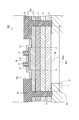
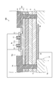
- FIG. 2 is a cross-sectional view showing the configuration of the compound semiconductor device 100 according to the first embodiment of the present invention, which is a cross-sectional view taken along the line II-II in FIG. 1.
- FIG. 7 is a cross-sectional view showing a first step of the method for manufacturing compound semiconductor device 100 in the first embodiment of the present invention.
- FIG. 7 is a cross-sectional view showing a second step of the method for manufacturing compound semiconductor device 100 in the first embodiment of the present invention.
- FIG. 9 is a cross sectional view showing a third step of the method for manufacturing compound semiconductor device 100 in the first embodiment of the present invention.
- FIG. 9 is a cross-sectional view showing a fourth step of the method for manufacturing compound semiconductor device 100 in the first embodiment of the present invention.
- FIG. 9 is a cross-sectional view showing a fifth step of the method for manufacturing compound semiconductor device 100 in the first embodiment of the present invention.
- FIG. 9 is a cross sectional view showing a sixth step of the method for manufacturing compound semiconductor device 100 in the first embodiment of the present invention.
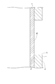
- FIG. 13 is a cross-sectional view showing the method of manufacturing compound semiconductor device 100 in the first modification of the first embodiment of the present invention.
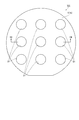
- FIG. 9 is a cross-sectional view showing a configuration of a compound semiconductor device 100 according to a second modification of the first embodiment of the present invention. It is a top view which shows the structure of the compound semiconductor substrate 101 in the 2nd Embodiment of this invention, and is a top view at the time of seeing from the lower surface side of the Si substrate 1.
- FIG. 12 is a cross-sectional view showing the structure of the compound semiconductor substrate 101 according to the second embodiment of the present invention, which is a cross-sectional view taken along line XII-XII in FIG. 11.
- FIG. 1 is a plan layout of each member of the compound semiconductor device 100 according to the first embodiment of the present invention, showing a plan layout viewed from a direction orthogonal to the upper surface 1a of the Si substrate 1.
- FIG. 2 is a cross-sectional view showing the configuration of compound semiconductor device 100 according to the first embodiment of the present invention, which is a cross-sectional view taken along the line II-II in FIG.
- compound semiconductor device 100 (an example of a compound semiconductor device) in the present embodiment includes a GaN-HEMT (High Electron Mobility Transistor) as a semiconductor device. It is preferable that this HEMT is used for high frequencies (a high frequency voltage of about several gigahertz is applied to the gate electrode). However, it goes without saying that the present invention can be applied to semiconductor devices other than high frequency applications.
- GaN-HEMT High Electron Mobility Transistor
- the compound semiconductor device 100 includes a Si substrate 1 (an example of a Si substrate), a SiC layer 3 (an example of a crystal layer), an AlN (aluminum nitride) buffer layer 5 (an example of a nitride layer not containing Ga), and AlGaN. (Aluminum gallium nitride) buffer layer 7, GaN layer 9, AlGaN layer 11, source electrode 13 (an example of a first electrode), drain electrode 15 (an example of a second electrode), and gate electrode 17 (an example). An example of a third electrode) and an insulating layer 19 are provided.
- the GaN layer 9 and the AlGaN layer 11 constitute a Ga nitride layer 10 (an example of a wide-gap semiconductor layer) which is a nitride layer containing Ga.
- HEMT is formed on the Ga nitride layer 10.
- the Si substrate 1 has an annular planar shape that surrounds a hole (through hole) 21 (an example of a hole) when viewed two-dimensionally (from a direction orthogonal to the upper surface 1a of the Si substrate).
- the (111) plane is exposed on the upper surface 1 a of the Si substrate 1.
- the (100) plane or the (110) plane may be exposed on the upper surface 1a of the Si substrate 1.
- the hole 21 may have any planar shape, and may have a rectangular planar shape or a circular planar shape. Assuming a circle having the same area as the bottom area of the hole 21, the circle has a diameter of 1 mm or more and 50 mm or less, preferably 10 mm or less.
- the size of the hole 21 may be determined according to the mechanical strength required for the compound semiconductor device 100.
- the Si substrate 1 has a thickness of 200 ⁇ m or more and 1.5 mm or less (length in a direction orthogonal to the upper surface 1a of the Si substrate).
- the SiC layer 3 is in contact with the Si substrate 1 and is formed on the upper surface 1 a of the Si substrate 1.
- the SiC layer 3 covers the hole 21, and the lower surface 3b of the SiC layer 3 is exposed at the bottom of the hole 21.
- the SiC layer 3 is not formed on the side surface of the hole 21 of the Si substrate 1.
- the SiC layer 3 includes, for example, at least one of 2H (hexagonal) -SiC, 3C (cubic) -SiC, 4H (hexagonal) -SiC, 6H (hexagonal) -SiC, and 15R (rhombohedral) -SiC. It is preferable that it has a crystal structure. Particularly, when the SiC layer 3 is epitaxially grown on the upper surface 1a of the Si substrate 1, the SiC layer 3 is generally made of 3C-SiC, and the upper surface of the SiC layer 3 is the (111) plane.
- the upper surface of SiC layer 3 may be other than the (111) plane, such as the (110) plane and the (-1-1-1) plane.
- the SiC layer 3 has a thickness of 20 nm or more and 10 ⁇ m or less.
- the thickness of SiC layer 3 is preferably 100 nm or more and 3.5 ⁇ m or less.
- the thickness of SiC layer 3 is more preferably 500 nm or more and 2 ⁇ m or less.
- the SiC layer 3 is made of single crystal 3C—SiC, it may contain polycrystalline SiC or amorphous SiC in some regions.
- the SiC layer 3 is an example of a crystal layer.
- the crystal layer may be a covalent crystal layer, and may be a SiC layer, diamond, BN, or the like. SiC and diamond are classified as crystalline layers containing C.
- BN has a crystal structure such as a hexagonal layered structure, a cubic sphalerite structure, or a hexagonal wurtzite structure. From the viewpoint of improving high frequency characteristics, it is preferable that this crystal layer has a specific resistance of 100 ⁇ ⁇ cm or more or 100 m ⁇ ⁇ cm or less.
- This crystal layer more preferably has a specific resistance of 1000 ⁇ ⁇ cm or more or 10 m ⁇ ⁇ cm or less, further preferably 10000 ⁇ ⁇ cm or more or 1 m ⁇ ⁇ cm or less, or 10000 ⁇ ⁇ cm or more or 100 ⁇ ⁇ cm. It is more preferable to have the following specific resistance.
- the crystal layer has a specific resistance in the above range, it is possible to reduce the parasitic capacitance and the parasitic resistance in the compound semiconductor device 100, and the high frequency characteristics of the compound semiconductor device 100 become particularly good.
- the crystal layer contains SiC containing as impurities at least one of nitrogen and phosphorus that are N-type dopants, Al and B that are P-type dopants, and a transition metal that is a dopant that exhibits semi-insulating properties.
- the transition metal include Sc (scandium) and dopants such as Ti (titanium), V (vanadium), and Cr (chromium). Even if SiC is not intentionally doped, the SiC usually contains a small amount of nitrogen as an environmental substance. This environmental substance, nitrogen, is also included in the above-mentioned dopant.
- the above formulas (1) and (2) are the conditions to be satisfied when the resistance of the SiC layer is increased, and the above formula (3) is the condition to be satisfied when the resistance of the SiC layer is reduced.
- the AlN buffer layer 5 is in contact with the SiC layer 3 and is formed on the upper surface of the SiC layer 3.
- the AlN buffer layer 5 and the AlGaN buffer layer 7 serve as a buffer layer that relaxes the difference in the lattice constant and the difference in the thermal expansion coefficient between the SiC layer 3 and the GaN layer 9.
- the AlN buffer layer 5 has a thickness of, for example, 5 nm or more and 2 ⁇ m or less, and more preferably 100 nm or more and 1 ⁇ m or less.
- the AlGaN buffer layer 7 is in contact with the AlN buffer layer 5 and is formed on the upper surface of the AlN buffer layer 5.
- the AlGaN buffer layer 7 has a thickness of, for example, 500 nm or more and 2 ⁇ m or less, and more preferably 900 nm or more and 2 ⁇ m or less.
- the AlGaN buffer layer 7 may be omitted. Further, the AlGaN buffer layer 7 may be replaced with another buffer structure such as a superlattice structure.
- the GaN layer 9 is in contact with the AlGaN buffer layer 7 and is formed on the upper surface of the AlGaN buffer layer 7.
- the GaN layer 9 has a mesa structure and includes a convex portion 9a. Impurities are preferably not intentionally introduced near the interface between the GaN layer 9 and the AlGaN layer 11, and the interface between the GaN layer 9 and the AlGaN layer 11 serves as an electron transit layer of the HEMT.
- the GaN layer 9 has a thickness of, for example, 200 nm or more and 9 ⁇ m or less. More preferably, the GaN layer 9 has a thickness of 550 nm or more and 3 ⁇ m or less.
- a thin film layer of AlN or AlGaN may be appropriately inserted in the GaN layer 9.
- the total number of layers to be inserted is preferably 9 or less, more preferably 5 or less, and further preferably 3 or less.
- the AlGaN layer 11 is in contact with the upper surface of the convex portion 9a of the GaN layer 9, and is formed in a region (second element isolation region) RG2 partitioned by the convex portion 9a.
- the AlGaN layer 11 serves as a HEMT barrier layer.
- the AlGaN layer 11 has a thickness of, for example, 10 nm or more and 50 nm or less, and more preferably 20 nm or more and 40 nm or less.
- the SiC layer 3 serves as an underlayer of the Ga nitride layer 10.
- Ga nitride layer 10 may be formed on the upper surface side of SiC layer 3.
- the AlN buffer layer 5 and the AlGaN buffer layer 7 are formed between the SiC layer 3 and the Ga nitride layer 10, and the SiC forming the SiC layer 3 and the GaN forming the GaN layer 9 are formed.
- the AlN buffer layer 5 and the AlGaN buffer layer 7 may be omitted, and the Ga nitride layer 10 may be directly formed on the upper surface of the SiC layer 3.
- Each of the source electrode 13, the drain electrode 15, and the gate electrode 17 is formed on the upper surface side of the Ga nitride layer 10. Each of the source electrode 13 and the drain electrode 15 is formed on the upper surface of the AlGaN layer 11 with a space therebetween.
- the gate electrode 17 is formed between the source electrode 13 and the drain electrode 15 on the upper surface of the AlGaN layer 11. Each of the source electrode 13, the drain electrode 15, and the gate electrode 17 extends to the upper surface of the GaN layer 9.
- Each of the source electrode 13 and the drain electrode 15 is in ohmic contact with the AlGaN layer 11.
- the gate electrode 17 is in Schottky contact with the AlGaN layer 11, for example.
- Each of the source electrode 13 and the drain electrode 15 has, for example, a structure in which a Ti (titanium) layer and an Al layer are stacked in this order from the AlGaN layer 11 side.
- the gate electrode 17 has, for example, a structure in which a Ni (nickel) layer and an Au (gold) layer are stacked in this order from the AlGaN layer 11 side.
- a separation groove 22 is formed between the compound semiconductor device 100 and another adjacent compound semiconductor device.
- the compound semiconductor device 100 is electrically isolated from the adjacent compound semiconductor device by the separation groove 22.
- Each of the plurality of compound semiconductor devices 100 is formed in a region (first element isolation region) RG1 partitioned by the isolation trench 22.
- the isolation groove 22 is formed to a depth reaching the upper surface 1 a of the Si substrate 1 from the upper surface of the insulating layer 19.
- the separation groove that partitions the compound semiconductor layer 100 is preferably formed to a depth reaching the boundary between the AlGaN layer 11 and the GaN layer 9, and more preferably a depth reaching the AlGaN buffer layer 7.
- the depth reaching the AlN buffer layer 5 is more preferable, the depth reaching the SiC layer 3 is more preferable, and the depth reaching the upper surface 1a of the Si substrate 1 is further preferable.
- the separation groove 22 does not necessarily have to be formed.
- the insulating layer 19 does not necessarily have to be formed.
- ions may be implanted into the nitride layer in the region to increase the resistance of the region and use this as the isolation layer.
- the insulating layer 19 is formed on the GaN layer 9 and the AlGaN layer 11 so as to fill the separation groove 22.
- An opening 19a is formed in a required portion of the insulating layer 19, and the source electrode 13 and the drain electrode 15 are exposed at the bottom of the opening 19a.
- the insulating layer 19 is made of, for example, SiN (silicon nitride) or SiO 2 (silicon oxide).
- each layer forming the compound semiconductor device 100 is measured using, for example, a spectroscopic ellipsometer.
- the spectroscopic ellipsometer irradiates a measurement target with incident light that is polarized light, and receives reflected light from the measurement target. Since the S-polarized light and the P-polarized light have a phase shift and a difference in reflectance, the polarization state of the reflected light is different from the polarization state of the incident light. This change in the polarization state depends on the wavelength of incident light, the incident angle, the optical constant of the film, the film thickness, and the like.
- the spectroscopic ellipsometer calculates the optical constant and film thickness of the film from the obtained reflected light based on the wavelength and incident angle of the incident light. Needless to say, the thickness of each layer can be measured by a spectral reflection method, cross-sectional SEM observation, cross-sectional TEM observation, or the like.
- the operation of the HEMT of this embodiment is as follows.
- the source electrode 13 is always kept at the ground potential (reference potential).
- the voltage is not applied to the gate electrode 17, due to the difference in band gap between the GaN layer 9 and the AlGaN layer 11 and the polarization and stress of the AlGaN layer 11, the heterojunction between the GaN layer 9 and the AlGaN layer 11 occurs.
- a two-dimensional electron gas is formed at the bonding interface.
- a sufficient negative voltage is applied to the gate electrode 17, the above-mentioned two-dimensional electron gas is removed from the heterojunction interface between the GaN layer 9 and the AlGaN layer 11, and thus the drain electrode 15 to the source electrode 13 is removed. No current flows.
- the concentration of the two-dimensional electron gas increases due to the electric field effect.
- the current flowing from the drain electrode 15 to the source electrode 13 increases. Therefore, the current flowing between the source electrode 13 and the drain electrode 15 can be controlled by the voltage applied to the gate electrode 17.
- the Ga nitride layer 10 is formed on the surface of the first nitride layer and the first nitride layer, and has a bandgap wider than that of the first nitride layer.
- the second nitride layer may be included as long as it includes the second nitride layer, and may be formed of a combination of nitride semiconductor materials other than the combination of GaN and AlGaN (for example, two types of AlGaN layers having different Al composition ratios). Good.
- a hole 21 is formed in a region (a region directly under the HEMT) overlapping with the source electrode 13, the drain electrode 15, and the gate electrode 17 when viewed from a direction orthogonal to the upper surface 1a of the Si substrate 1. It is provided and the Si substrate 1 does not exist. As described above, in the compound semiconductor device 100, the Si substrate directly below the semiconductor device is removed.
- the Si substrate is metallized at a temperature of at most about 200 ° C.
- the underlying Si substrate exists immediately below the compound semiconductor device, if the semiconductor device generates heat during operation of the compound semiconductor device, the underlying Si substrate having a high resistance.
- the specific resistance of gradually decreases and passes through the range of the specific resistance where the power loss becomes large. Therefore, it is difficult to suppress the power loss of the compound semiconductor device.
- the compound semiconductor device 100 according to the present embodiment since such an Si substrate does not exist immediately below the compound semiconductor device 100, the power loss can be suppressed even if the compound semiconductor device generates heat. You can As a result, a HEMT having good high frequency characteristics can be realized.
- a plurality of functional elements may be built inside the side wall of the region (hole 21) where the Si substrate is removed.
- a disk-shaped Si substrate 1 (where holes 21 (FIG. 1) are not formed) is prepared. Then, the SiC layer 3, the AlN buffer layer 5, the AlGaN buffer layer 7, the GaN layer 9, and the AlGaN layer 11 are formed in this order on the upper surface 1a of the Si substrate 1.
- the SiC layer 3 is formed by carbonizing the upper surface 1a of the Si substrate 1, and is formed on the underlayer made of SiC to form an MBE (Molecular Beam Epitaxy) method, a CVD (Chemical Vapor Deposition) method, or an LPE (Liquid Phase Phase) epitaxy. It may be formed by homoepitaxial growth of SiC using a method or the like. SiC layer 3 may be formed only by carbonizing the surface of Si substrate 1. Furthermore, SiC layer 3 may be formed by heteroepitaxially growing SiC on the surface of Si substrate 1. A buffer layer may be formed prior to the heteroepitaxial growth.
- MBE Molecular Beam Epitaxy
- CVD Chemical Vapor Deposition
- LPE Liquid Phase Phase
- the AlN buffer layer 5 is formed by using, for example, a MOCVD (Metal Organic Chemical Vapor Deposition) method.
- the growth temperature of the AlN buffer layer 5 is, for example, 1000 ° C. or higher and lower than the Si melting point.
- the Al source gas for example, TMA (Tri Methyl Aluminum), TEA (Tri Ethyl Aluminum), DMAH (Di Methyl Aluminum Hydride), or the like is used.
- NH 3 (ammonia) is used as the nitrogen source gas, for example.
- the AlGaN buffer layer 7 is formed by using, for example, the MOCVD method.
- the growth temperature of the AlGaN buffer layer 7 is, for example, 1000 ° C. or higher and lower than the Si melting point.
- TMA or TEA is used as the Al source gas.
- the Ga source gas for example, TMG (Tri Methyl Gallium), TEG (Tri Ethyl Gallium), or the like is used.
- NH 3 is used as the nitrogen source gas.
- the GaN layer 9 is formed by using, for example, the MOCVD method.
- the growth temperature of the GaN layer 9 is, for example, 900 ° C. or higher and 1200 ° C. or lower.
- TMG or TEG is used as the Ga source gas.
- NH 3 is used as the nitrogen source gas.
- the AlGaN layer 11 is formed by, for example, the MOCVD method or the MBE method.
- the AlGaN layer 11 and the GaN layer 9 in the necessary regions are removed by performing etching from the upper surface side of the AlGaN layer 11.
- the convex portion 9a is formed in the GaN layer 9, and the excess AlGaN layer 11 existing other than the upper surface of the convex portion 9a is removed.
- a separation groove 22 is formed from the upper surface of the GaN layer 9 to the upper surface 1a of the Si substrate 1.
- the separation groove 22 is formed by a method such as mechanical grinding or etching.
- the source electrode 13 and the drain electrode 15 are each formed in a necessary region on the upper surface of each of the AlGaN layer 11 and the GaN layer 10 by using a normal photoengraving technique and an etching technique. ..
- the gate electrode 17 is formed in a necessary region on the upper surface of each of the AlGaN layer 11 and the GaN layer 10 by using a normal photolithography technique and an etching technique.
- Each of the source electrode 13, the drain electrode 15, and the gate electrode 17 is formed by, for example, a vapor deposition method, a MOCVD method, a sputtering method, or the like.
- a hole 21 is formed by removing Si in the central portion of the lower surface 1b of the Si substrate 1.
- the removal of Si is performed by mechanically grinding Si of the Si substrate 1.
- the removal of Si may be performed by forming a ring-shaped photoresist on the lower surface 1b of the Si substrate 1 and etching Si of the Si substrate 1 using the formed photoresist as a mask.
- Si removal may be performed by a combination of a plurality of methods such as mechanical grinding and wet etching.
- the lower surface 3b of the SiC layer 3 is exposed at the bottom of the hole 21.
- the final step of exposing the lower surface 3b of the SiC layer 3 is preferably wet etching or dry etching.
- a protective layer on the surface on the electrode formation surface side.
- the protective layer include a photoresist, a polyimide coating agent, a polyimide film, and a PVC film.
- the protective film described above is peeled off after the formation of the holes or during the formation of the holes (after mechanical grinding or the like). After peeling, the electrode formation surface is cleaned, such as organic cleaning, if necessary.
- the Si substrate 1 is isotropically etched.
- the inner wall surface of the hole 21 in the Si substrate 1 is inclined, and the width of the Si substrate 1 (the length in the horizontal direction in FIG. 7) becomes narrower as the distance from the SiC layer 3 increases.
- the holes 21 may be formed at any timing after the SiC layer 3 is formed. After forming the hole 21, each of the source electrode 13, the drain electrode 15, and the gate electrode 17 may be formed.
- an insulating layer 19 is formed so as to fill the inside of the separation groove 22 and cover each of the GaN layer 9, the AlGaN layer 11, the source electrode 13, and the drain electrode 15.
- an opening 19a is formed in a necessary region of the insulating layer 19 by using a normal photoengraving technique and an etching technique, and the compound semiconductor device 100 shown in FIGS. 1 and 2 is completed. ..
- the inside of the separation groove 22 does not have to be filled with an insulating layer.
- the separation groove 22 does not necessarily have to be formed. Instead of forming the isolation trench 22, ions may be implanted into the nitride layer in the region to increase the resistance of the region and use this as the isolation layer.
- the Ga nitride layer 10 is made of an ionic crystal, and the atoms in the Ga nitride layer 10 are connected to each other by an electric attraction.
- an ionic crystal has a hard property, but has a cleavability (a property of being brittle and easily broken). Therefore, when an external force is applied to the Ga nitride layer 10, cracks are likely to occur in the Ga nitride layer 10.
- the SiC layer 3 is made of a covalent bond crystal, and each atom in the SiC layer 3 is connected to each other by a covalent bond.
- a covalent bond crystal has a low cleavability, and the crack generation principle of the covalent bond crystal is different from the crack generation principle of the ionic crystal. As a result, the occurrence of cracks in the Ga nitride layer 10 is suppressed by the SiC layer 3, and the mechanical strength of the compound semiconductor device 100 can be improved.
- a crystal composed only of typical non-metal elements excluding hydrogen, halogen group elements and rare gas elements is defined as a covalent bond crystal. That is, B (boron), C (carbon), Si (silicon), N (nitrogen), P (phosphorus), As (arsenic), O (oxygen), S (sulfur), Se (selenium), Te (tellurium). ) Is defined as a covalent crystal.
- the SiC layer 3 is supported from below by the Si substrate 1 having an annular planar shape. Therefore, the mechanical strength of the SiC layer 3 can be reinforced by the Si substrate 1, and the mechanical strength of the compound semiconductor device 100 can be improved.
- the SiC layer 3 has an annular planar shape. It is supported by the Si substrate 1. Therefore, the mechanical strength of SiC layer 3 can be reinforced by Si substrate 1, and the generation of cracks in SiC layer 3 at the time of forming hole 21 can be suppressed. As a result, the yield at the time of manufacturing the compound semiconductor device 100 can be improved.
- the mechanical strength of the compound semiconductor device 100 can be improved, and the yield at the time of manufacturing the compound semiconductor device 100 can be improved, so that the size of the hole 21 can be enlarged.
- a large-area device can be realized on a structure without a Si substrate.
- a device without a Si substrate has less deterioration in high-frequency characteristics during high-temperature operation, and a large-area device can have a longer gate width, which increases the current value at which the device can operate. be able to. Therefore, it is possible to manufacture a device that can operate with a large current with a high yield, with little deterioration in high-frequency characteristics during high-temperature operation.
- the Si substrate 1 is removed in the upper region of the hole 21, a structure having no lateral current path through the inside of the Si substrate 1 is formed. Therefore, in the first embodiment, by doping the AlN buffer layer 5, the AlGaN buffer layer 7, and the GaN layer 9 with C or a transition metal, or by not intentionally doping these layers, If these layers have sufficiently high resistance, parasitic conduction between the source electrode 13 and the drain electrode 15 of the compound semiconductor device 100 can be sufficiently suppressed, as compared with the case where the hole 21 is not formed. The breakdown voltage of the device can also be improved.
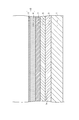
- FIG. 9 is a cross-sectional view showing the method of manufacturing the compound semiconductor device 100 according to the first modification of the first embodiment of the present invention.
- the first modification is a modification of the method for manufacturing compound semiconductor device 100 in the above-described embodiment.
- the first modified example after forming the SiC layer 3 and before forming the Ga nitride layer 10 and the like, by removing Si in the central portion of the lower surface 1b of the Si substrate 1, a plurality of holes is formed. 21 is formed.
- the SiC layer 3 is supported by the Si substrate 1 having an annular planar shape, and the mechanical strength of the SiC layer 3 is reinforced by the Si substrate 1. Even before the Ga nitride layer 10 is formed, the Si substrate 1 and the SiC layer 3 have sufficient mechanical strength, and the generation of cracks in the SiC layer 3 can be suppressed. This makes it possible to realize a structure in which a plurality of holes 21 are formed in the upper surface of the Si substrate and none of the SiC layers exposed at the bottoms of the plurality of holes 21 are damaged.
- the holes 21 after forming the Ga nitride layer 10 and the like as in the above-described embodiment. This is because the holes 21 can be formed while the mechanical strength of the SiC layer 3 is reinforced by the Si substrate 1 and the Ga nitride layer 10.
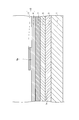
- FIG. 10 is a cross-sectional view showing the configuration of the compound semiconductor device 100 according to the second modification of the first embodiment of the present invention.
- compound semiconductor device 100 in the second modified example further includes metal layer 23 (an example of a metal layer), and thus the compound of the above-described embodiment shown in FIGS. 1 and 2. It is different from a semiconductor device.
- Metal layer 23 is formed at least at the bottom of hole 21, and is in contact with lower surface 3b of SiC layer 3.
- the metal layer 23 is electrically connected to the source electrode 13.
- the metal layer 23 is preferably grounded.
- the metal layer 23 is formed by, for example, a vapor deposition method, a MOCVD method, a sputtering method, or the like.
- the metal layer 23 may be electrically connected to the drain electrode 15 instead of the source electrode 13.
- the configuration of the compound semiconductor device 100 of the second modification other than the above is the same as the configuration of the compound semiconductor device of the first embodiment shown in FIG. 1, so the same members are designated by the same reference numerals. , The description will not be repeated.
- the metal layer 23 is provided immediately below the semiconductor device, and by grounding this metal layer, the ground plane (electrical ground) capable of preventing loss of high frequency power is a device. Is formed immediately below.
- the specific resistances of the SiC layer 3, the AlN buffer layer 5, the AlGaN buffer layer 7, and the GaN layer 9 are formed immediately below.
- FIG. 11 is a plan view showing the configuration of the compound semiconductor substrate 101 according to the second embodiment of the present invention, as viewed from the lower surface side of the Si substrate 1.
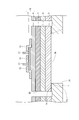
- FIG. 12 is a cross-sectional view showing the structure of the compound semiconductor substrate 101 according to the second embodiment of the present invention, which is a cross-sectional view taken along line XII-XII of FIG.
- compound semiconductor substrate 101 (an example of a compound semiconductor substrate) in the present embodiment is an intermediate structure which is a structure that appears in the process of manufacturing the compound semiconductor device in the first embodiment. It includes a plurality of 101a.
- the compound semiconductor substrate 101 includes a Si substrate 1 having a plane size (diameter) of about 2 inches to 12 inches, more preferably 4 inches to 8 inches, a SiC layer 3, an AlN buffer layer 5, and an AlGaN buffer layer 7. , GaN layer 9.
- the Si substrate 1 has a shape that surrounds the hole (through hole for the Si substrate) 21 when viewed in plan (from the direction orthogonal to the upper surface 1a of the Si substrate).
- the intermediate structure 101a is provided corresponding to each of the plurality of holes 21.
- the SiC layer 3, the AlN buffer layer 5, the AlGaN buffer layer 7, and the GaN layer 9 are formed on the upper surface 1a of the Si substrate 1 in this order.
- the SiC layer 3 is formed on the upper surface 1 a of the Si substrate 1 and covers the plurality of holes 21.
- the bottom surface 3b of the SiC layer 3 is exposed at the bottom of the plurality of holes 21.
- the size and shape of each of the plurality of holes 21 may be the same or different from each other.
- compound semiconductor substrate 101 of the present embodiment AlGaN layer 11 and GaN layer 9 in necessary regions are removed, source electrode 13, drain electrode 15, and gate electrode 17 are formed, and insulating layer 11 is formed. By forming the necessary grooves 11a, a plurality of compound semiconductor devices 100 can be obtained.
- the isolation trench 22 may not be formed in the compound semiconductor substrate 101 (that is, the isolation trench 22 may be formed after the compound semiconductor substrate 101 is completed).
- the compound semiconductor substrate 101 may further include the source electrode 13, the drain electrode 15, and the gate electrode 17 shown in FIG. In this case, the hole 21 exists in the region overlapping with the source electrode 13, the drain electrode 15, and the gate electrode 17 when viewed from the direction orthogonal to the upper surface 1a of the Si substrate 1, and the Si substrate 1 does not exist. ..
- the compound semiconductor substrate 101 may include at least the Si substrate 1 and the SiC layer 3.
- compound semiconductor substrate 101 other than the above is the same as the configuration of compound semiconductor device 100 in the first embodiment, and therefore description thereof will not be repeated.
- compound semiconductor substrate 101 since compound semiconductor substrate 101 includes a plurality of intermediate body structures 101a, it is possible to obtain the same effect as the compound semiconductor device according to the first embodiment.
- the SiC layer 3 is supported from below by the Si substrate 1, generation of cracks in the SiC layer 3 and the Ga nitride layer 10 during manufacturing is suppressed, and the SiC layer 3 is exposed at the bottom of each of the holes 21. The SiC layer 3 is not damaged. Therefore, the yield at the time of manufacturing can be improved.
- the step of forming the source electrode 13, the drain electrode 15, and the gate electrode 17, and the step of forming the separation groove 22 are carried out in a clean environment such as a clean room, for example, because dust is disliked. In the compound semiconductor substrate 101 shown in FIGS.
- the wide-gap semiconductor layer containing Ga semiconductor layer having a bandgap of 2.2 eV or more
- the wide-gap semiconductor layer containing Ga is GaN.
- an oxide such as Ga 2 O 3 may be used.
- Ga 2 O 3 has a bandgap energy larger than that of SiC or GaN, and is expected as a next-generation compound. Since Ga 2 O 3 has better breakdown voltage characteristics than GaN, a compound semiconductor device that employs Ga 2 O 3 as a wide-gap semiconductor layer containing Ga is suitable for a power device.
- GaN has a higher mobility than Ga 2 O 3, the compound semiconductor device that adopts GaN as the wide gap semiconductor layer containing Ga is suitable for a high frequency device.
- the compound semiconductor device includes the HEMT as the semiconductor device.
- the compound semiconductor device includes a MOSFET (Metal-Oxide-Semiconductor Field-Effect Transistor) and a MISFET (Metal-Insulator-Semiconductor-Semiconductor Fector). It may include a semiconductor device such as an effect transistor or a JFET (junction field effect transistor).
- the compound semiconductor device may be a vertical device of a type in which a current is passed in the thickness direction of the nitride semiconductor layer.
- Si substrate (an example of Si substrate) 1a Upper surface of Si substrate 1b Lower surface of Si substrate 3 SiC (silicon carbide) layer (an example of a crystal layer) 3b Lower surface of SiC layer 5 AlN (aluminum nitride) buffer layer (an example of a nitride layer not containing Ga) 7 AlGaN (aluminum gallium nitride) buffer layer 7 9 GaN (gallium nitride) layer 9a Convex portion of GaN layer 10 Ga (gallium) nitride layer (an example of wide-gap semiconductor layer) 11 AlGaN Layer 13 Source Electrode (Example of First Electrode) 15 Drain electrode (an example of the second electrode) 17 Gate electrode (an example of the third electrode) 19 Insulating Layer 19a Insulating Layer Opening 21 Hole (Example of Hole) 22 separation groove 23 metal layer (an example of metal layer) 100 compound semiconductor device (an example of compound semiconductor device) 101 compound semiconductor substrate (an example of compound semiconductor substrate) 101a
Landscapes
- Junction Field-Effect Transistors (AREA)
Abstract
La présente invention concerne un dispositif semi-conducteur composite, un substrat semi-conducteur composite, et un procédé de fabrication d'un dispositif semi-conducteur composite permettant d'augmenter la résistance mécanique, d'améliorer le rendement pendant la production et de mettre en œuvre un dispositif ayant une grande surface. Un dispositif semi-conducteur composite 100 comprend : un substrat de Si 1 dont la forme entoure un orifice 21 dans une vue en plan ; une couche de SiC 3 qui est formée sur une surface supérieure 1a du substrat de Si 1 et recouvre l'orifice 21 ; une couche de nitrure 10 qui comprend du Ga et est formée sur un côté surface supérieure de la couche de SiC 3 ; une électrode source 13 qui est formée sur un côté surface supérieure de la couche de nitrure 10 ; une électrode de drain 15 ; et une électrode de grille 17. Le courant électrique qui circule entre l'électrode de source 13 et l'électrode de drain 15 peut être commandé par une tension appliquée à l'électrode de grille 17. Le substrat de Si n'est pas présent dans une zone RG qui chevauche l'électrode de source 13, l'électrode de drain 15 et l'électrode de grille 17 vue depuis une direction perpendiculaire à la surface supérieure 1a du substrat de Si 1.
Priority Applications (4)
| Application Number | Priority Date | Filing Date | Title |
|---|---|---|---|
| CN201980072627.9A CN112997283A (zh) | 2018-11-01 | 2019-10-30 | 化合物半导体装置、化合物半导体基板以及化合物半导体装置的制造方法 |
| KR1020217016593A KR102735277B1 (ko) | 2018-11-01 | 2019-10-30 | 화합물 반도체 장치, 화합물 반도체 기판, 및 화합물 반도체 장치의 제조방법 |
| EP19878888.7A EP3876267A4 (fr) | 2018-11-01 | 2019-10-30 | Dispositif semi-conducteur composite, substrat semi-conducteur composite, et procédé de fabrication de dispositif semi-conducteur composite |
| US17/290,145 US12087852B2 (en) | 2018-11-01 | 2019-10-30 | Compound semiconductor device, compound semiconductor substrate, and method for manufacturing compound semiconductor device |
Applications Claiming Priority (2)
| Application Number | Priority Date | Filing Date | Title |
|---|---|---|---|
| JP2018-206717 | 2018-11-01 | ||
| JP2018206717A JP7248410B2 (ja) | 2018-11-01 | 2018-11-01 | 化合物半導体装置、化合物半導体基板、および化合物半導体装置の製造方法 |
Publications (1)
| Publication Number | Publication Date |
|---|---|
| WO2020090870A1 true WO2020090870A1 (fr) | 2020-05-07 |
Family
ID=70463232
Family Applications (1)
| Application Number | Title | Priority Date | Filing Date |
|---|---|---|---|
| PCT/JP2019/042524 Ceased WO2020090870A1 (fr) | 2018-11-01 | 2019-10-30 | Dispositif semi-conducteur composite, substrat semi-conducteur composite, et procédé de fabrication de dispositif semi-conducteur composite |
Country Status (7)
| Country | Link |
|---|---|
| US (1) | US12087852B2 (fr) |
| EP (1) | EP3876267A4 (fr) |
| JP (1) | JP7248410B2 (fr) |
| KR (1) | KR102735277B1 (fr) |
| CN (1) | CN112997283A (fr) |
| TW (1) | TWI850275B (fr) |
| WO (1) | WO2020090870A1 (fr) |
Families Citing this family (3)
| Publication number | Priority date | Publication date | Assignee | Title |
|---|---|---|---|---|
| CN116960150A (zh) * | 2022-04-19 | 2023-10-27 | 联华电子股份有限公司 | 高电子迁移率晶体管 |
| TW202414543A (zh) | 2022-07-27 | 2024-04-01 | 日商新唐科技日本股份有限公司 | 半導體裝置及半導體裝置之製造方法 |
| US20250393277A1 (en) * | 2024-06-25 | 2025-12-25 | Analog Devices, Inc. | Transistor device with metal backside field plate |
Citations (7)
| Publication number | Priority date | Publication date | Assignee | Title |
|---|---|---|---|---|
| JP2006216671A (ja) * | 2005-02-02 | 2006-08-17 | Toshiba Corp | 窒素化合物半導体素子 |
| JP2007087992A (ja) * | 2005-09-20 | 2007-04-05 | Showa Denko Kk | 半導体素子および半導体素子製造方法 |
| JP2010098251A (ja) | 2008-10-20 | 2010-04-30 | Fujitsu Ltd | 半導体装置及びその製造方法 |
| JP2013243275A (ja) | 2012-05-22 | 2013-12-05 | Pawdec:Kk | GaN系半導体素子およびその製造方法 |
| US20160260699A1 (en) * | 2015-03-06 | 2016-09-08 | Infineon Technologies Austria Ag | Method of Manufacturing Semiconductor Devices by Bonding a Semiconductor Disk on a Base Substrate, Composite Wafer and Semiconductor Device |
| WO2017069087A1 (fr) * | 2015-10-21 | 2017-04-27 | エア・ウォーター株式会社 | Substrat semi-conducteur composite pourvu d'une couche de sic |
| JP2017150064A (ja) | 2016-02-19 | 2017-08-31 | エア・ウォーター株式会社 | 化合物半導体基板、ペリクル膜、および化合物半導体基板の製造方法 |
Family Cites Families (17)
| Publication number | Priority date | Publication date | Assignee | Title |
|---|---|---|---|---|
| JP4746825B2 (ja) | 2003-05-15 | 2011-08-10 | 富士通株式会社 | 化合物半導体装置 |
| EP1831919A2 (fr) | 2004-10-28 | 2007-09-12 | Nitronex Corporation | Circuits integres monolithiques hyperfrequences a base de nitrure de gallium |
| WO2007034761A1 (fr) * | 2005-09-20 | 2007-03-29 | Showa Denko K.K. | Dispositif à semi-conducteur et son procédé de fabrication |
| US7745848B1 (en) * | 2007-08-15 | 2010-06-29 | Nitronex Corporation | Gallium nitride material devices and thermal designs thereof |
| JP5401788B2 (ja) * | 2007-12-28 | 2014-01-29 | 富士通株式会社 | 窒化物半導体装置及びその製造方法 |
| JP5468761B2 (ja) | 2008-09-25 | 2014-04-09 | 古河電気工業株式会社 | 半導体装置、ウエハ構造体および半導体装置の製造方法 |
| KR101015787B1 (ko) * | 2009-02-25 | 2011-02-18 | 전자부품연구원 | 방열 구조를 갖는 트랜지스터 및 그의 제조 방법 |
| US8421082B1 (en) | 2010-01-19 | 2013-04-16 | Mcube, Inc. | Integrated CMOS and MEMS with air dielectric method and system |
| JP2012038885A (ja) * | 2010-08-06 | 2012-02-23 | Panasonic Corp | 半導体装置及びその製造方法 |
| JP6156015B2 (ja) | 2013-09-24 | 2017-07-05 | 三菱電機株式会社 | 半導体装置及びその製造方法 |
| US9362198B2 (en) * | 2014-04-10 | 2016-06-07 | Freescale Semiconductor, Inc. | Semiconductor devices with a thermally conductive layer and methods of their fabrication |
| US9859225B2 (en) | 2015-05-15 | 2018-01-02 | Skyworks Solutions, Inc. | Backside cavity formation in semiconductor devices |
| US9685545B2 (en) * | 2015-11-25 | 2017-06-20 | Texas Instruments Incorporated | Isolated III-N semiconductor devices |
| US20200152455A1 (en) * | 2016-02-19 | 2020-05-14 | Air Water Inc. | A Compound Semiconductor Substrate, A Pellicle Film, And A Method For Manufacturing A Compound Semiconductor Substrate |
| CN108699687B (zh) | 2016-02-19 | 2022-03-01 | 爱沃特株式会社 | 化合物半导体基板、表膜、和化合物半导体基板的制造方法 |
| US10020270B2 (en) | 2016-09-29 | 2018-07-10 | Infineon Technologies Ag | Semiconductor device including a LDMOS transistor, monolithic microwave integrated circuit and method |
| US9929107B1 (en) | 2016-12-06 | 2018-03-27 | Infineon Technologies Ag | Method for manufacturing a semiconductor device |
-
2018
- 2018-11-01 JP JP2018206717A patent/JP7248410B2/ja active Active
-
2019
- 2019-10-30 WO PCT/JP2019/042524 patent/WO2020090870A1/fr not_active Ceased
- 2019-10-30 CN CN201980072627.9A patent/CN112997283A/zh active Pending
- 2019-10-30 KR KR1020217016593A patent/KR102735277B1/ko active Active
- 2019-10-30 EP EP19878888.7A patent/EP3876267A4/fr active Pending
- 2019-10-30 US US17/290,145 patent/US12087852B2/en active Active
- 2019-11-01 TW TW108139634A patent/TWI850275B/zh active
Patent Citations (7)
| Publication number | Priority date | Publication date | Assignee | Title |
|---|---|---|---|---|
| JP2006216671A (ja) * | 2005-02-02 | 2006-08-17 | Toshiba Corp | 窒素化合物半導体素子 |
| JP2007087992A (ja) * | 2005-09-20 | 2007-04-05 | Showa Denko Kk | 半導体素子および半導体素子製造方法 |
| JP2010098251A (ja) | 2008-10-20 | 2010-04-30 | Fujitsu Ltd | 半導体装置及びその製造方法 |
| JP2013243275A (ja) | 2012-05-22 | 2013-12-05 | Pawdec:Kk | GaN系半導体素子およびその製造方法 |
| US20160260699A1 (en) * | 2015-03-06 | 2016-09-08 | Infineon Technologies Austria Ag | Method of Manufacturing Semiconductor Devices by Bonding a Semiconductor Disk on a Base Substrate, Composite Wafer and Semiconductor Device |
| WO2017069087A1 (fr) * | 2015-10-21 | 2017-04-27 | エア・ウォーター株式会社 | Substrat semi-conducteur composite pourvu d'une couche de sic |
| JP2017150064A (ja) | 2016-02-19 | 2017-08-31 | エア・ウォーター株式会社 | 化合物半導体基板、ペリクル膜、および化合物半導体基板の製造方法 |
Non-Patent Citations (2)
| Title |
|---|
| P.STRIVASTAVA ET AL.: "Record Breakdown Voltage (2200 V) ofGaN DHFETs on Si With 2- m Buffer Thickness by Local Substrate Removal", IEEE ELECTRON DEVICE LETT., vol. 32, no. 1, January 2011 (2011-01-01), pages 30 - 32, XP011340566, DOI: 10.1109/LED.2010.2089493 |
| See also references of EP3876267A4 |
Also Published As
| Publication number | Publication date |
|---|---|
| KR20210082523A (ko) | 2021-07-05 |
| US20220005945A1 (en) | 2022-01-06 |
| TW202036915A (zh) | 2020-10-01 |
| JP7248410B2 (ja) | 2023-03-29 |
| CN112997283A (zh) | 2021-06-18 |
| EP3876267A4 (fr) | 2022-05-04 |
| US12087852B2 (en) | 2024-09-10 |
| KR102735277B1 (ko) | 2024-11-28 |
| TWI850275B (zh) | 2024-08-01 |
| JP2020072216A (ja) | 2020-05-07 |
| EP3876267A1 (fr) | 2021-09-08 |
Similar Documents
| Publication | Publication Date | Title |
|---|---|---|
| US9954087B2 (en) | Field effect transistor, and multilayered epitaxial film for use in preparation of field effect transistor | |
| JP6025213B2 (ja) | フローティングおよびグランドされた基板領域を備えるhemt | |
| US20160372609A1 (en) | Schottky barrier diode | |
| US12142643B2 (en) | Material structure for low thermal resistance silicon-based gallium nitride microwave and millimeter-wave devices and manufacturing method thereof | |
| US11189687B2 (en) | Semiconductor devices and methods of manufacturing the same | |
| CN113471284A (zh) | N极性GaN晶体管结构的制备方法和半导体结构 | |
| WO2019194042A1 (fr) | Procédé de fabrication d'un transistor | |
| JP2010199597A (ja) | 化合物半導体装置の製造方法 | |
| US12087852B2 (en) | Compound semiconductor device, compound semiconductor substrate, and method for manufacturing compound semiconductor device | |
| US10332975B2 (en) | Epitaxial substrate for semiconductor device and method for manufacturing same | |
| US20150021666A1 (en) | Transistor having partially or wholly replaced substrate and method of making the same | |
| US8558280B2 (en) | Semiconductor device and method of manufacturing the semiconductor device | |
| JP5608969B2 (ja) | 化合物半導体装置及びその製造方法 | |
| TWI523148B (zh) | 提升高電子遷移率電晶體元件崩潰電壓的方法 | |
| JP2016092169A (ja) | 半導体装置およびその製造方法 | |
| CN116325092B (zh) | 半导体器件及其制作方法 | |
| JP5972917B2 (ja) | 空間的に閉じ込められた誘電体領域を含む半導体構造 | |
| CN116762177A (zh) | 半导体结构及其制备方法、电子设备 | |
| TWI754463B (zh) | 具有環境保護性晶粒墊的半導體及製造具有環境保護性晶粒墊的半導體之方法 | |
| CN111653473B (zh) | 一种散热增强的硅基氮化镓微波器件材料结构 | |
| RU2534442C1 (ru) | Способ изготовления мощного свч-транзистора | |
| CN115663015B (zh) | 一种半导体器件结构及其制备方法 | |
| RU2507634C1 (ru) | Полупроводниковый прибор и способ его изготовления | |
| WO2025018137A1 (fr) | Dispositif à semi-conducteur au nitrure | |
| JP2024166957A (ja) | 窒化物半導体デバイス |
Legal Events
| Date | Code | Title | Description |
|---|---|---|---|
| 121 | Ep: the epo has been informed by wipo that ep was designated in this application |
Ref document number: 19878888 Country of ref document: EP Kind code of ref document: A1 |
|
| NENP | Non-entry into the national phase |
Ref country code: DE |
|
| ENP | Entry into the national phase |
Ref document number: 20217016593 Country of ref document: KR Kind code of ref document: A |
|
| ENP | Entry into the national phase |
Ref document number: 2019878888 Country of ref document: EP Effective date: 20210601 |