WO2020111202A1 - 表示装置および電子機器 - Google Patents
表示装置および電子機器 Download PDFInfo
- Publication number
- WO2020111202A1 WO2020111202A1 PCT/JP2019/046664 JP2019046664W WO2020111202A1 WO 2020111202 A1 WO2020111202 A1 WO 2020111202A1 JP 2019046664 W JP2019046664 W JP 2019046664W WO 2020111202 A1 WO2020111202 A1 WO 2020111202A1
- Authority
- WO
- WIPO (PCT)
- Prior art keywords
- layer
- display device
- electrode
- insulating layer
- interface
- Prior art date
- Legal status (The legal status is an assumption and is not a legal conclusion. Google has not performed a legal analysis and makes no representation as to the accuracy of the status listed.)
- Ceased
Links
Images

















Classifications
-
- H—ELECTRICITY
- H01—ELECTRIC ELEMENTS
- H01B—CABLES; CONDUCTORS; INSULATORS; SELECTION OF MATERIALS FOR THEIR CONDUCTIVE, INSULATING OR DIELECTRIC PROPERTIES
- H01B1/00—Conductors or conductive bodies characterised by the conductive materials; Selection of materials as conductors
- H01B1/02—Conductors or conductive bodies characterised by the conductive materials; Selection of materials as conductors mainly consisting of metals or alloys
-
- H—ELECTRICITY
- H10—SEMICONDUCTOR DEVICES; ELECTRIC SOLID-STATE DEVICES NOT OTHERWISE PROVIDED FOR
- H10K—ORGANIC ELECTRIC SOLID-STATE DEVICES
- H10K50/00—Organic light-emitting devices
- H10K50/80—Constructional details
- H10K50/84—Passivation; Containers; Encapsulations
- H10K50/844—Encapsulations
-
- H—ELECTRICITY
- H05—ELECTRIC TECHNIQUES NOT OTHERWISE PROVIDED FOR
- H05B—ELECTRIC HEATING; ELECTRIC LIGHT SOURCES NOT OTHERWISE PROVIDED FOR; CIRCUIT ARRANGEMENTS FOR ELECTRIC LIGHT SOURCES, IN GENERAL
- H05B33/00—Electroluminescent light sources
- H05B33/12—Light sources with substantially two-dimensional [2D] radiating surfaces
-
- H—ELECTRICITY
- H05—ELECTRIC TECHNIQUES NOT OTHERWISE PROVIDED FOR
- H05B—ELECTRIC HEATING; ELECTRIC LIGHT SOURCES NOT OTHERWISE PROVIDED FOR; CIRCUIT ARRANGEMENTS FOR ELECTRIC LIGHT SOURCES, IN GENERAL
- H05B33/00—Electroluminescent light sources
- H05B33/12—Light sources with substantially two-dimensional [2D] radiating surfaces
- H05B33/22—Light sources with substantially two-dimensional [2D] radiating surfaces characterised by the chemical or physical composition or the arrangement of auxiliary dielectric or reflective layers
-
- H—ELECTRICITY
- H10—SEMICONDUCTOR DEVICES; ELECTRIC SOLID-STATE DEVICES NOT OTHERWISE PROVIDED FOR
- H10K—ORGANIC ELECTRIC SOLID-STATE DEVICES
- H10K50/00—Organic light-emitting devices
- H10K50/10—OLEDs or polymer light-emitting diodes [PLED]
- H10K50/11—OLEDs or polymer light-emitting diodes [PLED] characterised by the electroluminescent [EL] layers
-
- H—ELECTRICITY
- H10—SEMICONDUCTOR DEVICES; ELECTRIC SOLID-STATE DEVICES NOT OTHERWISE PROVIDED FOR
- H10K—ORGANIC ELECTRIC SOLID-STATE DEVICES
- H10K50/00—Organic light-emitting devices
- H10K50/80—Constructional details
- H10K50/805—Electrodes
- H10K50/81—Anodes
-
- H—ELECTRICITY
- H10—SEMICONDUCTOR DEVICES; ELECTRIC SOLID-STATE DEVICES NOT OTHERWISE PROVIDED FOR
- H10K—ORGANIC ELECTRIC SOLID-STATE DEVICES
- H10K50/00—Organic light-emitting devices
- H10K50/80—Constructional details
- H10K50/85—Arrangements for extracting light from the devices
- H10K50/852—Arrangements for extracting light from the devices comprising a resonant cavity structure, e.g. Bragg reflector pair
-
- H—ELECTRICITY
- H10—SEMICONDUCTOR DEVICES; ELECTRIC SOLID-STATE DEVICES NOT OTHERWISE PROVIDED FOR
- H10K—ORGANIC ELECTRIC SOLID-STATE DEVICES
- H10K50/00—Organic light-emitting devices
- H10K50/80—Constructional details
- H10K50/88—Terminals, e.g. bond pads
-
- H—ELECTRICITY
- H10—SEMICONDUCTOR DEVICES; ELECTRIC SOLID-STATE DEVICES NOT OTHERWISE PROVIDED FOR
- H10K—ORGANIC ELECTRIC SOLID-STATE DEVICES
- H10K59/00—Integrated devices, or assemblies of multiple devices, comprising at least one organic light-emitting element covered by group H10K50/00
- H10K59/10—OLED displays
- H10K59/12—Active-matrix OLED [AMOLED] displays
- H10K59/121—Active-matrix OLED [AMOLED] displays characterised by the geometry or disposition of pixel elements
-
- H—ELECTRICITY
- H10—SEMICONDUCTOR DEVICES; ELECTRIC SOLID-STATE DEVICES NOT OTHERWISE PROVIDED FOR
- H10K—ORGANIC ELECTRIC SOLID-STATE DEVICES
- H10K59/00—Integrated devices, or assemblies of multiple devices, comprising at least one organic light-emitting element covered by group H10K50/00
- H10K59/10—OLED displays
- H10K59/12—Active-matrix OLED [AMOLED] displays
- H10K59/122—Pixel-defining structures or layers, e.g. banks
-
- H—ELECTRICITY
- H10—SEMICONDUCTOR DEVICES; ELECTRIC SOLID-STATE DEVICES NOT OTHERWISE PROVIDED FOR
- H10K—ORGANIC ELECTRIC SOLID-STATE DEVICES
- H10K59/00—Integrated devices, or assemblies of multiple devices, comprising at least one organic light-emitting element covered by group H10K50/00
- H10K59/10—OLED displays
- H10K59/12—Active-matrix OLED [AMOLED] displays
- H10K59/124—Insulating layers formed between TFT elements and OLED elements
-
- H—ELECTRICITY
- H10—SEMICONDUCTOR DEVICES; ELECTRIC SOLID-STATE DEVICES NOT OTHERWISE PROVIDED FOR
- H10K—ORGANIC ELECTRIC SOLID-STATE DEVICES
- H10K59/00—Integrated devices, or assemblies of multiple devices, comprising at least one organic light-emitting element covered by group H10K50/00
- H10K59/80—Constructional details
- H10K59/875—Arrangements for extracting light from the devices
- H10K59/876—Arrangements for extracting light from the devices comprising a resonant cavity structure, e.g. Bragg reflector pair
-
- H—ELECTRICITY
- H10—SEMICONDUCTOR DEVICES; ELECTRIC SOLID-STATE DEVICES NOT OTHERWISE PROVIDED FOR
- H10K—ORGANIC ELECTRIC SOLID-STATE DEVICES
- H10K2102/00—Constructional details relating to the organic devices covered by this subclass
- H10K2102/301—Details of OLEDs
- H10K2102/302—Details of OLEDs of OLED structures
- H10K2102/3023—Direction of light emission
- H10K2102/3026—Top emission
-
- H—ELECTRICITY
- H10—SEMICONDUCTOR DEVICES; ELECTRIC SOLID-STATE DEVICES NOT OTHERWISE PROVIDED FOR
- H10K—ORGANIC ELECTRIC SOLID-STATE DEVICES
- H10K2102/00—Constructional details relating to the organic devices covered by this subclass
- H10K2102/301—Details of OLEDs
- H10K2102/351—Thickness
-
- H—ELECTRICITY
- H10—SEMICONDUCTOR DEVICES; ELECTRIC SOLID-STATE DEVICES NOT OTHERWISE PROVIDED FOR
- H10K—ORGANIC ELECTRIC SOLID-STATE DEVICES
- H10K59/00—Integrated devices, or assemblies of multiple devices, comprising at least one organic light-emitting element covered by group H10K50/00
- H10K59/30—Devices specially adapted for multicolour light emission
-
- H—ELECTRICITY
- H10—SEMICONDUCTOR DEVICES; ELECTRIC SOLID-STATE DEVICES NOT OTHERWISE PROVIDED FOR
- H10K—ORGANIC ELECTRIC SOLID-STATE DEVICES
- H10K59/00—Integrated devices, or assemblies of multiple devices, comprising at least one organic light-emitting element covered by group H10K50/00
- H10K59/80—Constructional details
- H10K59/805—Electrodes
- H10K59/8051—Anodes
- H10K59/80518—Reflective anodes, e.g. ITO combined with thick metallic layers
-
- H—ELECTRICITY
- H10—SEMICONDUCTOR DEVICES; ELECTRIC SOLID-STATE DEVICES NOT OTHERWISE PROVIDED FOR
- H10K—ORGANIC ELECTRIC SOLID-STATE DEVICES
- H10K59/00—Integrated devices, or assemblies of multiple devices, comprising at least one organic light-emitting element covered by group H10K50/00
- H10K59/80—Constructional details
- H10K59/805—Electrodes
- H10K59/8052—Cathodes
- H10K59/80524—Transparent cathodes, e.g. comprising thin metal layers
Definitions
- the present disclosure relates to display devices and electronic devices.
- OLEDs Organic Electro-Luminescence Diodes
- Patent Document 1 proposes a technique in which an insulating film is provided in an inter-element region between a plurality of light emitting elements, and a groove is provided in a position between adjacent light emitting elements in the insulating film.
- Patent Document 2 proposes a technique of forming at least a part of a film thickness region of an insulating layer with a positively charged inorganic nitride.
- An object of the present disclosure is to provide a display device and an electronic device that can suppress a leakage of a drive current that occurs between adjacent light emitting elements.
- a first disclosure is a silicon compound, which is provided between a plurality of first electrodes provided for each pixel and a first electrode and covers a peripheral portion of the first electrode. Provided on the interface between the first electrode and the insulating layer, and the first interface layer including the first silicon oxide, and provided on the first electrode and the insulating layer in common for all pixels.
- the display device includes an organic layer including a light emitting layer and a second electrode provided on the organic layer, and the insulating layer includes the second silicon oxide on the surface portion on the organic layer side.
- a plurality of first electrodes provided for each pixel, an insulating layer provided between the first electrodes and containing a silicon compound, and a side surface of the first electrode and a side surface of the insulating layer.
- a first interface layer including a first silicon oxide, a first electrode and an insulating layer that are provided in common for all pixels, and an organic layer including a light emitting layer, and an organic layer that is provided on the organic layer.
- a second electrode, and the thickness of the organic layer on the first electrode is substantially constant.
- a plurality of first electrodes provided for each pixel, an insulating layer provided between the first electrodes, and a side surface of the first electrode and a side surface of the insulating layer are provided.
- the organic layer has a substantially constant thickness on the electrode.
- the fourth disclosure is an electronic device including the display device according to any one of the first to third disclosures.
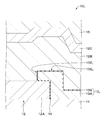
- FIG. 11 is a cross-sectional view showing an example of a configuration of a display device according to a modified example 1 of the first embodiment of the present disclosure.
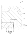
- FIG. 11 is a cross-sectional view showing an example of a configuration of a display device according to a modified example 2 of the first embodiment of the present disclosure.
- FIG. 11 is a cross-sectional view showing an example of a configuration of a display device according to Modification 3 of the first embodiment of the present disclosure.
- FIG. 16 is a cross-sectional view showing an example of a configuration of a display device according to a modified example 4 of the first embodiment of the present disclosure.
- FIG. 16 is a cross-sectional view showing an example of a configuration of a display device according to a modified example 5 of the first embodiment of the present disclosure.
- FIG. 6 is a cross-sectional view showing an example of a configuration of a display device according to a second embodiment of the present disclosure. It is sectional drawing which expands and represents a part of display apparatus shown in FIG. It is sectional drawing which expands and represents a part of display apparatus which concerns on a comparative example.
- FIG. 15A, FIG. 15B, FIG. 15C, FIG. 15D, FIG. 15E, and FIG. 15F are cross-sectional views showing an example of the manufacturing process of the display device.
- 16A, 16B, 16C, and 16D are cross-sectional views showing an example of the manufacturing process of the display device.
- FIG. 16 is a cross-sectional view showing an example of a configuration of a display device according to a modified example of the second embodiment of the present disclosure.
- FIG. 16 is a cross-sectional view showing an example of a configuration of a display device according to a modified example of the second embodiment of the present disclosure.
- FIG. 8 is a cross-sectional view showing an enlarged part of a display device according to a third embodiment of the present disclosure. It is sectional drawing which expands and represents a part of display device which concerns on a modification.
- 20A, 20B, and 20C are cross-sectional views showing an example of a manufacturing process of a display device.
- 21A, 21B, and 21C are cross-sectional views showing an example of a manufacturing process of a display device.
- FIG. 16 is a cross-sectional view showing an example of a configuration of a display device according to a modified example of the third embodiment of the present disclosure. It is sectional drawing which shows an example of a structure of the display apparatus which concerns on the 4th Embodiment of this indication.
- FIG. 24A is a cross-sectional view showing a part of the display device shown in FIG. 23 in an enlarged manner.
- FIG. 24B is a cross-sectional view showing an enlarged part of the display device according to the modification.
- FIG. 25A is a schematic cross-sectional view for explaining the first example of the resonator structure.
- FIG. 25B is a schematic sectional view for explaining the second example of the resonator structure.
- FIG. 26A is a schematic cross-sectional view for explaining the third example of the resonator structure.
- FIG. 26B is a schematic sectional view for explaining the fourth example of the resonator structure.
- FIG. 27A is a schematic cross-sectional view for explaining the fifth example of the resonator structure.
- FIG. 27B is a schematic sectional view for explaining the sixth example of the resonator structure. It is a typical sectional view for explaining the 7th example of a resonator structure. It is a top view showing an example of a schematic structure of a module.
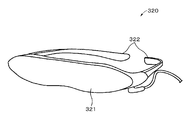
- FIG. 30A is a front view showing an example of the external appearance of a digital still camera.
- FIG. 30B is a rear view showing an example of the outer appearance of the digital still camera.
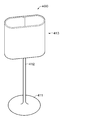
- It is a perspective view of an example of the appearance of a head mounted display. It is a perspective view which shows an example of the external appearance of a television apparatus. It is a perspective view showing an example of the appearance of a lighting installation.
- FIG. 30A is a front view showing an example of the external appearance of a digital still camera.
- FIG. 30B is a rear view showing an example of the outer appearance of the digital still camera.
- It is a perspective view of an example of the appearance of a head mounted display.
- It is a perspective view which shows
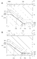
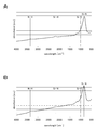
- FIG. 34A is a diagram showing an absorption spectrum of a bulk layer measured by a Fourier transform infrared spectrophotometer.
- FIG. 34B is a diagram showing an absorption spectrum of a bulk layer measured by a Fourier transform infrared spectrophotometer. The relationship between the peak intensity I NH derived from the NH bond and the peak intensity ratio I Si-H derived from the Si—H bond (I NH /I Si-H ) and the leak amount between pixels is shown. It is a graph.
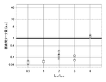
- FIG. 36 is a graph showing the relationship between the average thickness of the first interface layer and the leak amount between pixels. 7 is a graph showing evaluation results of luminous efficiency of the display devices of Examples 5-1 to 5-4 and Comparative example 5-1.
- FIG. 34B is a diagram showing an absorption spectrum of a bulk layer measured by a Fourier transform infrared spectrophotometer. The relationship between the peak intensity I NH derived from the NH bond and the peak intensity ratio I Si-H derived
- FIG. 38A is a diagram showing a model of an electromagnetic field simulation of Example 6-1.
- FIG. 38B is a diagram showing a model of the electromagnetic field simulation of Example 6-2.
- FIG. 39A is a diagram showing a model of an electromagnetic field simulation of Comparative Example 6-1.
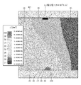
- FIG. 39B is a diagram showing a model of the electromagnetic field simulation of Comparative Example 6-2. It is a figure which shows the analysis result of the electromagnetic field simulation of Example 6-1. It is a figure which expands and represents the area
- FIG. 16 is a diagram showing an analysis result of an electromagnetic field simulation of Example 6-2. It is a figure which expands and represents the area
- FIG. 11 is a diagram showing an analysis result of an electromagnetic field simulation of Comparative Example 6-2. It is a figure which expands and represents the area
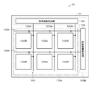
- FIG. 1 illustrates an example of the overall configuration of an organic EL (Electro-Luminescence) display device 10 (hereinafter, simply referred to as “display device 10”) according to a first embodiment of the present disclosure.
- the display device 10 is suitable for use in various electronic devices, and a display area 110A and a peripheral area 110B are provided on the periphery of the display area 110A on the substrate 11.
- a plurality of sub-pixels 100R, 100G, 100B are arranged in a matrix in the display area 110A.
- the sub-pixel 100R displays red
- the sub-pixel 100G displays green
- the sub-pixel 100B displays blue.
- the sub-pixels 100R, 100G, and 100B are referred to as the sub-pixel 100 unless otherwise specified.
- the columns of sub-pixels 100R, 100G, and 100B that display the same color are repeatedly arranged in the row direction. Therefore, the combination of the three sub-pixels 100R, 100G, and 100B arranged in the row direction configures one pixel.
- a signal line driving circuit 120 and a scanning line driving circuit 130 which are drivers for video display, are provided.
- the signal line drive circuit 120 supplies a signal voltage of a video signal according to the brightness information supplied from a signal supply source (not shown) to the selected pixel via the signal line 120A.
- the scanning line drive circuit 130 is composed of a shift register or the like that sequentially shifts (transfers) the start pulse in synchronization with the input clock pulse.
- the scanning line driving circuit 130 scans each pixel in units of rows when writing a video signal to each pixel and sequentially supplies the scanning signal to each scanning line 130A.
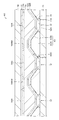
- FIG. 2 is a sectional view showing an example of the configuration of the display device 10 according to the first embodiment of the present disclosure.
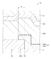
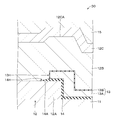
- FIG. 3 is a sectional view showing a part of the display device 10 shown in FIG. 2 in an enlarged manner.
- the display device 10 is a top emission type display device, and includes a substrate (first substrate) 11, a plurality of light emitting elements 12 and an insulating layer 13 provided on one main surface of the substrate 11, and a plurality of light emitting elements. 12, the protective layer 15 provided on the protective layer 15, the color filter 16 provided on the protective layer 15, the filling resin layer 17 provided on the color filter 16, and the counter substrate provided on the filling resin layer 17 ( Second substrate) 18.
- the counter substrate 18 side is the top side, and the substrate 11 side is the bottom side.
- the plurality of light emitting elements 12 are arranged in a matrix on one main surface of the substrate 11.
- the light emitting element 12 is a white organic EL light emitting element, and as a colorization method in the display device 10, a method using a white organic EL light emitting element and a color filter 16 is used. It should be noted that the colorization method is not limited to this, and an RGB coloring method or the like may be used. Alternatively, a monochromatic filter may be used.
- the light emitting element 12 is one in which, for example, a first electrode 12A as an anode, an organic layer 12B, and a second electrode 12C as a cathode are stacked in this order from the substrate 11 side.
- the substrate 11 is a support body that supports a plurality of light emitting elements 12 arranged on one main surface. Although not shown, the substrate 11 is provided with a driving circuit including a sampling transistor and a driving transistor for controlling driving of the plurality of light emitting elements 12, and a power supply circuit for supplying electric power to the plurality of light emitting elements 12. May be.
- the substrate 11 may be made of, for example, glass or resin having low moisture and oxygen permeability, or may be made of a semiconductor in which a transistor or the like can be easily formed.
- the substrate 11 is a glass substrate such as high strain point glass, soda glass, borosilicate glass, forsterite, lead glass, or quartz glass, a semiconductor substrate such as amorphous silicon or polycrystalline silicon, or polymethyl
- a resin substrate such as methacrylate, polyvinyl alcohol, polyvinyl phenol, polyether sulfone, polyimide, polycarbonate, polyethylene terephthalate, or polyethylene naphthalate.
- the board 11 is provided with a contact plug 11A.
- the contact plug 11A electrically connects the first electrode 12A to the drive circuit, the power supply circuit, and the like.
- the contact plug 11 ⁇ /b>A electrically connects the first electrode 12 ⁇ /b>A and a drive circuit, a power supply circuit, and the like (not shown) provided inside the substrate 11 so that the light emitting element 12 emits light. Is applied to the first electrode 12A.
- the contact plug 11A is, for example, chromium (Cr), gold (Au), platinum (Pt), nickel (Ni), copper (Cu), molybdenum (Mo), tungsten (W), titanium (Ti), tantalum (Ta). ), aluminum (Al), iron (Fe), or silver (Ag), or a simple substance of metal, such as an alloy, or a stacked layer of a plurality of these metal films.
- the first electrode 12A is provided separately for each of the sub-pixels 100R, 100G, 100B.
- the first electrode 12A also has a function as a reflective layer, and it is preferable that the first electrode 12A be composed of a metal layer having a reflectance as high as possible and a work function as large as possible in order to improve light emission efficiency.
- the constituent material of the metal layer for example, chromium (Cr), gold (Au), platinum (Pt), nickel (Ni), copper (Cu), molybdenum (Mo), titanium (Ti), tantalum (Ta), At least one of simple substance and alloy of metal elements such as aluminum (Al), magnesium (Mg), iron (Fe), tungsten (W), and silver (Ag) can be used. Specific examples of the alloy include AlNi alloy and AlCu alloy.
- the first electrode 12A may be composed of a laminated film of a plurality of metal layers containing at least one of the above simple substance of metal elements and alloys.
- the second electrode 12C is provided as an electrode common to all the sub-pixels 100R, 100G, 100B in the display area 110A.
- the second electrode 12C is a transparent electrode that is transparent to the light generated in the organic layer 12B.
- the transparent electrode also includes a semi-transmissive reflective film.
- the second electrode 12C is made of, for example, a metal or a metal oxide.
- the metal for example, at least one selected from a simple substance of metal elements such as aluminum (Al), magnesium (Mg), calcium (Ca), and sodium (Na) and an alloy thereof can be used.
- an alloy of magnesium (Mg) and silver (Ag) (MgAg alloy) or an alloy of aluminum (Al) and lithium (Li) (AlLi alloy) is suitable.
- the metal oxide for example, a mixture of indium oxide and tin oxide (ITO), a mixture of indium oxide and zinc oxide (IZO), zinc oxide (ZnO), or the like can be used. it can.
- the insulating layer 13 is for electrically separating the first electrode 12A for each of the sub-pixels 100R, 100G, and 100B.
- the insulating layer 13 is provided between the first electrodes 12A and covers the peripheral portion of the first electrodes 12A. More specifically, the insulating layer 13 has an opening at a portion corresponding to each first electrode 12A, and a peripheral portion of an upper surface of the first electrode 12A (a surface facing the second electrode 12C). To the side surface (end surface) of the first electrode 12A.
- a first interface layer 14 is provided at the interface between the first electrode 12A and the insulating layer 13.
- the insulating layer 13 includes a bulk layer 13A that serves as an insulating layer body, and a second interface layer 13B provided at the interface between the bulk layer 13A and the organic layer 12B.
- the bulk layer 13A is preferably positively charged. Since the bulk layer 13A is positively charged, it is possible to suppress the leak of the hole current generated between the adjacent light emitting elements 12.
- the bulk layer 13A contains a silicon compound as a main component.
- the main component refers to the one having the largest proportion of the material components contained in the bulk layer 13A.
- the silicon compound includes, for example, at least one selected from the group consisting of silicon nitride (SiN x ), silicon oxide (SiO x ), silicon oxynitride (SiO x N y ), and silicon carbide (SiC x ).
- silicon nitride SiN x
- SiO x silicon oxide
- SiO x N y silicon oxynitride
- SiC x silicon carbide
- the bulk layer 13A may further contain hydrogen (H).
- H hydrogen
- a Si-containing gas eg, SiH 4 etc.
- an N-containing gas eg, NH 2 , NH 3 etc.
- CVD Chemical Vapor Deposition
- the bulk layer 13A contains hydrogen contained in the source gas.
- the peak intensity I NH and Si—H bond derived from the N—H bond obtained by analyzing the bulk layer 13A with a Fourier transform infrared spectrophotometer (FT-IR) are obtained.
- the peak intensity ratio (I NH /I Si-H ) with the derived peak intensity I Si-H is preferably less than 4, and more preferably 3 or less.
- the peak intensity ratio (I NH /I Si-H ) is less than 4, the dipole formed at the interface with the first interface layer 14 can be increased. Therefore, the fixed charge of the insulating layer 13 can be increased and the insulating layer 13 can be effectively positively charged. Therefore, the leak of the hole current generated between the adjacent light emitting elements 12 can be further suppressed.
- the peak intensity ratio (I NH /I Si-H ) is calculated as follows. First, after the counter substrate 18 is peeled from the display device 10, the layers stacked on the bulk layer 13A are peeled off to expose the surface of the bulk layer 13A. Next, the bulk layer 13A is analyzed by FT-IR to acquire an FT-IR spectrum. Then, using the obtained FT-IR spectrum, the peak intensity ratio (I NH /I Si-H ) is obtained.
- the second interface layer 13B is for suppressing the leak of the hole current and the leak of the electron current which occur between the adjacent light emitting elements 12.
- the second interface layer 13B has a lattice strain, and thus the function of suppressing the leak of the hole current and the leak of the electron current described above is exhibited.
- the "lattice strain” is assumed to include the lattice strain of minute crystal grains contained in the second interface layer 13B.
- “leakage of hole current” means that holes injected from the first electrode 12A, which is an anode, travel through the interface between the insulating layer 13 and the organic layer 12B, and the adjacent first electrode 12A. It refers to the phenomenon that flows to.
- electrostatic current leakage includes a phenomenon in which electrons injected from the second electrode 12C, which is a cathode, travels through the organic layer 12B and flows to the adjacent first electrode 12A, or the organic layer 12B. This is a phenomenon in which electrons formed in the charge generation layer (for example, hole injection layer) flow along the organic layer 12B.
- the second interface layer 13B has a composition different from that of the bulk layer 13A. Specifically, the second interface layer 13B contains silicon oxide. The second interface layer 13B may further contain nitrogen (N). In this case, nitrogen forms a bond with silicon in the second interface layer 13B and may be present as silicon nitride or silicon oxynitride. Since the second interface layer 13B contains nitrogen, the second interface layer 13B easily causes lattice distortion, and the function of suppressing the above-described hole current leak and electron current leak can be further improved. ..
- the second interface layer 13B covers the main surface of the bulk layer 13A and the edge (end surface) of the bulk layer 13A.
- the second interface layer 13B preferably has a substantially uniform thickness over the entire layer from the viewpoint of improving the function of suppressing the leak of the hole current and the leak of the electron current described above.
- the upper limit of the average thickness of the second interface layer 13B is preferably 10 nm or less. When the average thickness of the second interface layer 13B is 10 nm or less, the relaxation of the lattice strain of the second interface layer 13B can be suppressed.
- the lower limit of the average thickness of the second interface layer 13B is preferably 2 nm or more.
- the average thickness of the second interface layer 13B is obtained in the same manner as the average thickness of the first interface layer 14 described later.
- the ratio of silicon oxide to the total amount of silicon oxide and silicon nitride in the second interface layer 13B is preferably 80% or more.
- the ratio is 80% or more, the lattice strain can be effectively generated in the second interface layer 13B due to the difference in composition between the bulk layer 13A and the second interface layer 13B. Therefore, the function of suppressing the leak of the hole current and the leak of the electron current described above can be further improved.
- the ratio of silicon oxide to the total amount of silicon oxide and silicon nitride is calculated as follows. First, a cross section of the display device 10 is cut out by the FIB method or the like to produce a thin piece. Next, the cross section of the thin piece is analyzed by electron energy loss spectroscopy (EELS) to determine the contents of silicon oxide and silicon nitride in the second interface layer 13B. Then, using these contents, the ratio of silicon oxide to the total amount of silicon oxide and silicon nitride is calculated.
- EELS electron energy loss spectroscopy
- the first interface layer 14 is for suppressing the exchange of elements forming the film between the first electrode 12A and the insulating layer 13, for example, the exchange of oxygen, and for suppressing the deterioration of the characteristics of the insulating layer 13. .. Specifically, for example, it is intended to suppress a decrease in fixed charges of the bulk layer 13A and keep the insulating layer 13 (specifically, the bulk layer 13A) positively charged.
- the first interface layer 14 has a composition different from that of the bulk layer 13A. Specifically, the first interface layer 14 contains silicon oxide.
- the average thickness of the first interface layer 14 is preferably 1 nm or more and less than 15 nm, more preferably 1 nm or more and 13 nm or less, still more preferably 1 nm or more, from the viewpoint of suppressing the leak of hole current between the adjacent light emitting elements 12. It is 9 nm or less, particularly preferably 1 nm or more and 7 nm or less, and most preferably 1 nm or more and 5 nm or less.
- the average thickness of the first interface layer 14 is obtained as follows. First, a cross section of the display device 10 is cut out by cryo-FIB (Focused Ion Beam) processing or the like to produce a thin piece. Then, the produced thin piece is observed by TEM (Transmission Electron Microscope), and one cross-sectional TEM image is acquired. At this time, the acceleration voltage was set to 80 kV. Next, in one acquired cross-sectional TEM image, the thickness of the portion of the first interface layer 14 covering the first electrode 12A (the portion of the region R in FIG. 3) was measured at 10 points or more. To do. At this time, each measurement position is randomly selected from the portion covering the first electrode 12A. Then, the film thickness of the first interface layer 14 measured at 10 points or more is simply averaged (arithmetic average) to obtain the average thickness of the first interface layer 14.
- the organic layer 12B is provided as an organic layer common to all the sub-pixels 100R, 100G and 100B in the display area 110A.
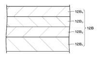
- FIG. 4 is an enlarged view of the organic layer 12B shown in FIG.
- the organic layer 12B has a structure in which a hole injection layer 12B 1 , a hole transport layer 12B 2 , a light emitting layer 12B 3 , and an electron transport layer 12B 4 are laminated in this order from the first electrode 12A side.
- the structure of the organic layer 12B is not limited to this, and layers other than the light emitting layer 12B 3 are provided as needed.
- the hole injection layer 12B 1 is a buffer layer for increasing the efficiency of hole injection into the light emitting layer 12B 3 and for suppressing leakage.
- the hole transport layer 12B 2 is for enhancing the efficiency of hole transport to the light emitting layer 12B 3 .
- the light emitting layer 12B 3 is a layer that emits light by recombination of electrons and holes when an electric field is applied.
- the electron transport layer 12B 4 is for enhancing the electron transport efficiency to the light emitting layer 12B 3 .
- An electron injection layer (not shown) may be provided between the electron transport layer 12B 4 and the second electrode 12C. This electron injection layer is for improving the electron injection efficiency.
- the protective layer 15 is for blocking the light emitting element 12 from the outside air and suppressing the infiltration of water from the outside environment into the light emitting element 12. Further, when the second electrode 12C is composed of a metal layer, the protective layer 15 also has a function of suppressing the oxidation of this metal layer.
- the protective layer 15 is, for example, silicon oxide (SiO x ), silicon nitride (SiN x ), silicon oxynitride (SiN x O y ), titanium oxide (TiO x ), aluminum oxide (Al x O y ), or the like. Is composed of an inorganic material having a low Further, the protective layer 15 may have a single-layer structure, but may have a multi-layer structure when the thickness is increased. This is to relieve the internal stress in the protective layer 15. Further, the protective layer 15 may be made of a polymer resin. In this case, as the polymer resin, at least one resin material of thermosetting resin and ultraviolet curable resin can be used.
- the color filter 16 is a so-called on-chip color filter (OCCF).
- the color filter 16 includes, for example, a red filter 16R, a green filter 16G, and a blue filter 16B.
- the red filter 16R, the green filter 16G, and the blue filter 16B are provided to face the light emitting element 12 of the sub pixel 100R, the light emitting element 12 of the sub pixel 100G, and the light emitting element 12 of the sub pixel 100B, respectively.
- the white light emitted from each of the light emitting elements 12 in the sub-pixel 100R, the sub-pixel 100G, and the sub-pixel 100B passes through the red filter 16R, the green filter 16G, and the blue filter 16B, respectively, and thereby the red light is emitted.
- Green light, and blue light are emitted from the display surface, respectively.
- a light shielding layer 16BM is provided between the color filters of each color, that is, in the region between the sub-pixels 100.
- the filling resin layer 17 is filled in the space between the protective layer 15 and the color filter 16.
- the filling resin layer 17 has a function as an adhesive layer that adheres the color filter 16 and the counter substrate 18 together.
- the filling resin layer 17 is made of at least one resin material of thermosetting resin and ultraviolet curable resin.
- the counter substrate 18 is provided so that one main surface of the counter substrate 18 and one main surface of the substrate 11 on which the plurality of light emitting elements 12 are provided face each other.
- the counter substrate 18 seals the light emitting element 12, the color filter 16 and the like together with the filling resin layer 17.
- the counter substrate 18 is made of a material such as glass that is transparent to each color light emitted from the color filter 16.
- a drive circuit and the like are formed on one main surface of the substrate 11 by using, for example, a thin film forming technique, a photolithography technique, and an etching technique.
- a metal layer on the drive circuit or the like by, for example, a sputtering method, patterning the metal layer by, for example, a photolithography technique and an etching technique, for each light emitting element 12 (that is, for each subpixel 100).
- a plurality of first electrodes 12A separated into two are formed.
- the first interface layer 14 is formed on one main surface of the substrate 11 on which the plurality of first electrodes 12A are formed by, for example, the CVD method, and then the bulk layer 13A is formed by, for example, the CVD method.
- the first interface layer 14 and the bulk layer 13A are patterned by using the photolithography technique and the etching technique.
- the surface of the bulk layer 13A is plasma-treated to form the second interface layer 13B, or the second interface layer 13B is formed on the bulk layer 13A by the ALD (Atomic Layer Deposition) method.
- the insulating layer 13 is obtained.
- the plasma treatment for example, oxygen plasma treatment or nitrogen plasma treatment can be used. Note that these plasma treatments may be used alone or in combination.
- the second interface layer 13B is formed on the bulk layer 13A by the ALD method, the second interface layer 13B is also formed on the first electrode 12A, but the surface of the first electrode 12A containing a metal material is formed. And the surface of the bulk layer 13A containing a silicon compound such as silicon nitride have different deposition efficiency of the precursor, and thus the second interface layer 13B is hardly formed on the first electrode 12A. Therefore, the second interface layer 13B formed on the first electrode 12A does not substantially affect the driving of the light emitting element 12. However, for the purpose of further quality structure, the second interface layer 13B formed on the first electrode 12A may be removed by using the photolithography technique and the etching technique.
- the hole injection layer 12B 1 , the hole transport layer 12B 2 , the light emitting layer 12B 3 , and the electron transport layer 12B 4 are laminated in this order on the first electrode 12A and the insulating layer 13 by, for example, a vapor deposition method.
- the organic layer 12B is formed.
- the second electrode 12C is formed on the organic layer 12B by, for example, a sputtering method.
- the plurality of light emitting elements 12 are formed on the one main surface of the substrate 11.
- the protective layer 15 is formed on the second electrode 12C by, for example, a vapor deposition method or a CVD method, and then the color filter 16 is formed on the protective layer 15.
- a flattening layer may be formed above, below, or both above and below the color filter 16 in order to flatten the step due to the film thickness difference of the protective layer 15 and the color filter 16 itself.
- the color filter 16 is covered with the filling resin layer 17 by, for example, an ODF (One Drop Fill) method, and then the counter substrate 18 is placed on the filling resin layer 17.
- ODF One Drop Fill
- the display device 10 is sealed.
- the filling resin layer 17 contains both a thermosetting resin and an ultraviolet curing resin
- the filling resin layer 17 is irradiated with ultraviolet rays to be temporarily cured, and then the filling resin layer 17 is heated to be fully cured. It may be allowed to.
- the display device 10 is provided between the plurality of first electrodes 12A provided for each sub-pixel 100 and the first electrode 12A, and the first electrode 12A is provided.
- the insulating layer 13 includes a bulk layer 13A containing a silicon compound as a main component, and a second interface layer 13B provided at the interface between the bulk layer 13A and the organic layer 12B and containing silicon oxide.
- the hole current and the electron current transmitted through the interface between the organic layer 12B and the insulating layer 13 can be suppressed. Therefore, it is possible to suppress a decrease in current light emission efficiency of the display device 10 and abnormal light emission color.
- FIG. 5 shows an example of the configuration of the display device 10 1 according to Modification 1 of the first embodiment of the present disclosure.
- Display device 10 instead of the insulating layer 13, in that an insulating layer 13 1 is different from the display device 10 according to the first embodiment.
- the insulating layer 13 1 includes a bulk layer 13A, a second interface layer 13B, and an intermediate layer 13C provided between the bulk layer 13A and the second interface layer 13B.
- the intermediate layer 13C is a layer for facilitating formation of fixed charges in the bulk layer 13A. It is preferable that the intermediate layer 13C contains silicon fluoride (SiFx) in order to have a biased charge. Whether or not the intermediate layer 13C contains silicon fluoride is determined by, for example, X-ray Photoelectron Spectroscopy (XPS) to determine the interface between the bulk layer 13A and the second interface layer 13B. It can be confirmed by analyzing.
- XPS X-ray Photoelectron Spectroscopy
- FIG. 6 illustrates an example of the configuration of the display device 10 2 according to the second modification of the first embodiment of the present disclosure.
- Display device 10 2 instead of the insulating layer 13, in that an insulating layer 13 2 is different from the display device 10 according to the first embodiment.
- the insulating layer 13 2 includes a bulk layer 13A and a second interface layer 13D having a two-layer structure provided on the bulk layer 13A.
- the second interface layer 13D includes a first layer 13D 1 and a second layer 13D 2 provided on the first layer 13D 1 .
- the first layer 13D 1 contains, for example, silicon oxide.
- the second layer 13D 2 contains, for example, at least one of silicon oxynitride and silicon nitride. The order of stacking the first layer 13D 1 and the second layer 13D 2 may be reversed.
- the display device 10 2 includes the second interface layer 13D having the two-layer structure, so that the lattice strain of the second interface layer 13D can be reduced by the second layer having the single-layer structure in the above-described first embodiment. It can be made larger than the lattice strain of the interface layer 13B. Therefore, the function of suppressing the leak of the hole current and the leak of the electron current can be further improved.
- the second interface layer 13D may have a laminated structure of two or more layers.
- at least one of the two or more layers may contain silicon oxide.
- at least one of the two or more layers may contain at least one of silicon oxynitride and silicon nitride.
- FIG. 7 shows an example of the configuration of the display device 10 3 according to Modification 3 of the first embodiment of the present disclosure.
- Display device 103 instead of the insulating layer 13, in that an insulating layer 13 3 is different from the display device 10 according to the first embodiment.
- Insulating layer 13 3 is provided with a bulk layer 13A, a second interface layer 13E provided on the bulk layer 13A.
- the side wall portion 13E 1 of the second interface layer 13E that covers the edge (end surface) of the bulk layer 13A has a different composition from the main surface portion 13E 2 of the second interface layer 13E that covers the main surface of the bulk layer 13A. ..
- “different composition” means different constituents, or the same constituent but different proportions of constituents.
- the side wall portion 13E 1 and the main surface portion 13E 2 include, for example, silicon oxide or silicon oxynitride having different compositions.
- the side wall portion 13E 1 has a positive fixed charge and is preferably positively charged. It is possible to prevent the hole flows through the upper surface of the insulating layer 13 3 along the edge of the insulating layer 13 3 from the first electrode 12A. Therefore, the leak of the hole current can be further suppressed.
- Examples of the constituent material of the side wall portion 13E 1 for giving a positive fixed charge include germanium oxide (GeO 2 ), yttrium oxide (Y 2 O 3 ), lutetium oxide (Lu 2 O 3 ), and lanthanum oxide (La). 2 O 3 ) and that containing at least one selected from the group consisting of strontium oxide (SrO) can be used.
- germanium oxide GeO 2
- Y 2 O 3 yttrium oxide
- Lu 2 O 3 lutetium oxide
- La lanthanum oxide
- SrO strontium oxide
- the second interface layer 13E having the above configuration is formed as follows, for example.
- an insulating layer containing a silicon compound as a main component is formed by a plasma CVD method.
- the flow rate ratio of the gas is adjusted to form a silicon oxide film on the surface of the insulating layer.
- the insulating layer is patterned by using a photolithography technique and an etching technique, and then a silicon oxide film is formed only on the side wall portion by, for example, vapor deposition.
- FIG. 8 shows an example of the configuration of a display device 10 4 according to Modification 4 of the first embodiment of the present disclosure.
- the display device 10 4 differs from the display device 10 according to the first embodiment in that a single insulating layer 13 4 is provided instead of the insulating layer 13 including the bulk layer 13A and the second interface layer 13B. ing.
- the insulating layer 13 4 contains a silicon compound as a main component in the bulk, and also contains silicon oxide in the surface portion on the organic layer 12B side.
- the “main component” refers to the one having the largest proportion of the material components contained in the insulating layer 13 4 .
- the silicon compound is the same as the silicon compound contained in the bulk layer 13A in the above-described first embodiment.
- the composition of the insulating layer 13 4 continuously changes, for example, from the bulk toward the outermost surface on the organic layer 12B side.
- the oxygen concentration of the insulating layer 13 4 (more specifically, the concentration of silicon oxide of the insulating layer 13 4 ) gradually increases from the bulk toward the outermost surface on the organic layer 12B side.
- the composition of the insulating layer 13 4 may continuously change from the bulk toward the edge-side surface. In this case, the function of suppressing the leak of the hole current and the leak of the electron current can be further improved.
- the silicon oxide is contained within a depth range of 10 nm or less from the outermost surface of the insulating layer 13 4 on the organic layer 12B side. This is because the lattice strain can be increased in the surface portion on the organic layer 12B side by changing the concentration of silicon oxide within a narrow range.
- Insulating layer 13 4 may further contain nitrogen in the surface portion of the organic layer 12B side.
- nitrogen may be present as silicon nitride or silicon oxynitride by forming a bond with silicon on the surface portion on the organic layer 12B side.
- the surface portion on the organic layer 12B side further contains nitrogen, the surface portion on the organic layer 12B side is likely to generate lattice distortion, and the function of suppressing the leak of hole current and the leak of electron current can be further improved. it can.
- the ratio of silicon oxide to the total amount of silicon oxide and silicon nitride in the surface portion on the organic layer 12B side is preferably 80% or more.
- the above ratio is 80% or more, lattice distortion can be effectively generated in the surface portion on the organic layer 12B side due to the difference in composition between the bulk of the insulating layer 13 and the surface portion on the organic layer 12B side. Therefore, the function of suppressing the leak of the hole current and the leak of the electron current described above can be further improved.
- the above ratio in the surface portion on the organic layer 12B side is obtained in the same manner as the ratio of silicon oxide to the total amount of silicon oxide and silicon nitride in the second interface layer 13B of the first embodiment described above.
- the second interface layer 13B is provided on the surface of the bulk layer 13A as in the first embodiment described above is adopted rather than the configuration in which the composition of the insulating layer 13 4 is continuously changed as described above.
- the provision of the second interface layer 13B promotes lattice distortion on the surface of the insulating layer 13 on the organic layer 12B side, and the leak suppressing effect can be further improved.
- FIG. 9 shows an example of a configuration of a display apparatus 105 according to a fifth modification of the first embodiment of the present disclosure.
- the display device 10 5 is different from the display device 10 according to the first embodiment in that the display device 10 5 includes a first electrode 12D having a laminated structure instead of the first electrode 12A having a single layer structure.
- the first electrode 12D includes a metal layer 12D 1 and a transparent oxide conductive layer 12D 2 provided on the metal layer 12D 1 .
- the metal layer 12D 1 is the same as the metal layer used as the first electrode 12A in the first embodiment.
- the oxide conductive layer 12D 2 includes a mixture of indium oxide and tin oxide (ITO), a mixture of indium oxide and zinc oxide (IZO), and a mixture of indium oxide, gallium oxide, and zinc oxide. It is preferable to contain at least one metal oxide selected from the group consisting of the body (IGZO). This is because these metal oxides have a high work function and can improve the hole injection property.
- the first interface layer 14 is particularly effective in the display device 10 5 including the first electrode 12D having the above configuration.
- the oxide conductive layer 12D 2 and the insulating layer 13 are adjacent to each other, exchange of elements (for example, oxygen) forming these layers is particularly likely to occur. Therefore, when the first interface layer 14 is provided, the effect of suppressing the exchange of the constituent elements of the film between the oxide conductive layer 12D 2 and the insulating layer 13 is remarkably exhibited.
- FIG. 10 is a cross-sectional view showing an example of the configuration of the display device 20 according to the second embodiment of the present disclosure.
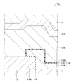
- FIG. 11 is a sectional view showing a part of the display device 20 shown in FIG. 10 in an enlarged manner.
- the display device 20 is different from the display device 10 according to the first embodiment in that the display device 20 includes an insulating layer 23 and a first interface layer 24 instead of the insulating layer 13 and the first interface layer 14.
- the insulating layer 23 is for electrically separating the first electrode 12A for each of the sub-pixels 100R, 100G, and 100B.
- the insulating layer 23 is provided between the side surfaces of the first electrodes 12A that are adjacent to each other in the in-plane direction of the substrate 11.
- the upper surface of the insulating layer 23 is flat. In the present specification, the “upper surface” refers to the surface that is the display surface side of the display device 20.
- the insulating layer 23 includes a bulk layer 23A serving as an insulating layer body and a second interface layer 23B provided at the interface between the bulk layer 23A and the organic layer 12B.
- a bulk layer 23A serving as an insulating layer body
- a second interface layer 23B provided at the interface between the bulk layer 23A and the organic layer 12B.
- the case where the insulating layer 23 includes the second interface layer 23B will be described, but the insulating layer 23 does not have to include the second interface layer 23B.
- the bulk layer 23A is provided between the side surfaces of the first electrodes 12A that are adjacent to each other in the in-plane direction of the substrate 11 without covering the peripheral portion of the first electrodes 12A. It is similar to the bulk layer 13A.
- the second interface layer 23B is similar to the second interface layer 13B in the first embodiment except that it is provided on the upper surface of the bulk layer 23A.
- the first interface layer 24 is provided between the side surface of the insulating layer 23 and the side surface of the first electrode 12A.
- the upper surface of the first interface layer 24 is flat.
- the first interface layer 24 is the same as the first interface layer 14 in the first embodiment.
- the thickness of the organic layer 12B on the first electrode 12A is substantially constant. That is, the upper surface of the organic layer 12B on the first electrode 12A is substantially flat. As a result, a vertical leak (in FIG. 11) between the first electrode 12A and the second electrode 12C (specifically, a portion of the second electrode 12C corresponding to the first electrode 12A). (See arrow I 1 ) can be suppressed.
- a concave portion 12BA is formed in a portion of the upper surface of the organic layer 12B corresponding to the peripheral portion of the first electrode 12A, and the thickness of the organic layer 12B on the first electrode 12A is increased.
- a portion between the first electrode 12A and the second electrode 12C is provided. Electric field concentrates. As a result, a vertical leak (in FIG. 11) between the first electrode 12A and the second electrode 12C (specifically, a portion of the second electrode 12C corresponding to the first electrode 12A). The arrow I 1 ) becomes larger.
- longitudinal leak refers to hole current leak and electron current leak between the first electrode 12A and the second electrode 12C in the thickness direction of the organic layer 12B.
- the thickness of the organic layer 12B on the first electrode 12A is substantially constant
- the variation in the thickness of the organic layer 12B on the first electrode 12A is the same as that of the organic layer 12B on the first electrode 12A. It is within ⁇ 5% of the average thickness.
- the upper surface of the organic layer 12B is substantially flat means that the displacement of the upper surface of the organic layer 12B (displacement in the thickness direction of the organic layer 12B) is within ⁇ 5% of the average thickness of the organic layer 12B.
- the thickness and average thickness of the organic layer 12B are obtained in the same manner as the thickness and average thickness of the first interface layer 14 in the first embodiment.
- the height H 1 of the organic layer 12B on the first electrode 12A and the height H 2 of the organic layer 12B in the peripheral portion of the first electrode 12A satisfy the relationship of H 1 ⁇ H 2 .
- This can prevent the electric field from being concentrated on a part between the first electrode 12A and the second electrode 12C. Therefore, the vertical leakage (FIG. 11) between the first electrode 12A and the second electrode 12C (specifically, the portion of the second electrode 12C corresponding to the portion around the first electrode 12A).
- the arrow I 2 can be suppressed.
- the height H 1 of the organic layer 12B on the first electrode 12A and the height H 2 of the organic layer 12B in the peripheral portion of the first electrode 12A are H
- the electric field is concentrated on a part between the first electrode 12A and the second electrode 12C.
- a vertical leak (specifically, a portion of the second electrode 12C corresponding to a portion around the first electrode 12A) between the first electrode 12A and the second electrode 12C ( The arrow I 2 in FIG. 13) becomes larger.
- the “portion around the first electrode 12A” means a range of 50 nm or less from the side surface of the first electrode 12A.
- the height H 1 of the organic layer 12B on the first electrode 12A, the height H 21 of the organic layer 12B on the first interface layer 24, and the height H 22 of the organic layer in the portion around the first electrode 12A may be satisfied. Also in this case, the vertical leak (see the arrow I 2 in FIG. 11) can be suppressed.
- FIG. 14 an example in which the height H 1 of the organic layer 12B on the first electrode 12A and the height H 2 of the organic layer 12B in the peripheral portion of the first electrode 12A are H 1 ⁇ H 2 is shown. It is shown.
- the organic layer 12B on the first electrode 12A is not formed. It is possible to obtain the organic layer 12B in which the height H 1 and the height H 2 of the organic layer 12B in the portion around the first electrode 12A satisfy the relationship of H 1 ⁇ H 2 . Therefore, the vertical leak can be suppressed as described above.
- a substrate 11 including a driving circuit and the like is formed by using, for example, a thin film forming technique, a photolithography technique, and an etching technique.
- an electrode layer 12A1 such as a metal layer or a metal oxide layer is formed on the substrate 11 by, for example, a sputtering method, and then the electrode layer 12A1 is formed by using, for example, a photolithography technique and an etching technique.
- FIG. 15C By patterning, as shown in FIG. 15C, a plurality of first electrodes 12A separated for each light emitting element 12 (that is, for each subpixel 100) are formed.
- a first interface layer 24 is formed on one main surface of the substrate 11 on which a plurality of first electrodes 12A are formed, for example, by the CVD method, and then, for example, by the etch back method.
- the first interface layer 24 is removed so that the first interface layer 24 remains on the side surface of the first electrode 12A.
- a bulk layer 23A is formed on one main surface of the substrate 11 by CVD, for example, so as to cover the first electrode 12A and the first interface layer 24.
- a photoresist layer 23A1 is formed on the bulk layer 23A by, for example, spin coating, and the surface is flattened.
- the photoresist layer 23A1 is removed and a part of the bulk layer 23A is removed by, for example, an etch-back method to remove the first electrode 12A and the first interface 12A having substantially the same thickness.
- the layer 24 and the bulk layer 23A are formed.
- a second interface layer 23B is formed as shown in FIG. 16C, or the second interface layer 23B is bulk-processed by an ALD (Atomic Layer Deposition) method. It is formed on the upper surface of the layer 23A. Thereby, the insulating layer 23 is obtained.
- ALD Atomic Layer Deposition
- the hole injection layer 12B 1 , the hole transport layer 12B 2 , the light emitting layer 12B 3 , and the electron transport layer 12B 4 are laminated in this order on the first electrode 12A and the insulating layer 23 by, for example, a vapor deposition method.
- the organic layer 12B having a substantially flat upper surface is formed.
- the display device 20 is obtained by performing the other steps in the same manner as in the method of manufacturing the display device 10 according to the first embodiment.
- the thickness of the organic layer 12B on the first electrode 12A is substantially constant and the height of the organic layer 12B on the first electrode 12A is high. is h 1, and the height h 2 of the organic layer 12B is around the portion of the first electrode 12A, satisfies the relationship of h 1 ⁇ h 2.
- This can prevent the electric field from being concentrated on a part between the first electrode 12A and the second electrode 12C. Therefore, it is possible to suppress the occurrence of vertical leakage (see arrows I 1 and I 2 in FIG. 11) due to electric field concentration.
- the thickness of the organic layer 12B on the first electrode 12A is substantially constant, it is possible to suppress the occurrence of color shift due to a change in film thickness (cavity shift) of the organic layer 12B.
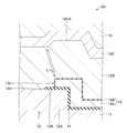
- FIG. 18 is a cross-sectional view showing an enlarged part of the display device 30 according to the third embodiment of the present disclosure.
- the organic layer 12B has a plurality of convex portions 12CA on the upper surface.
- the plurality of convex portions 12CA are provided in the portions corresponding to the peripheral portions of the plurality of first electrodes 12A, respectively.
- the thickness of the organic layer 12B in the region inside the convex portion 12CA is substantially constant.
- the first interface layer 14 has a plurality of openings (first openings) 14H respectively provided on the plurality of first electrodes 12A.
- the insulating layer 13 has a plurality of openings (second openings) 13H respectively provided on the plurality of first electrodes 12A.
- the peripheral edge of the opening 14H is located inside the peripheral edge of the opening 13H. That is, the first interface layer 14 has a protrusion 14A that protrudes from the peripheral edge of the opening 13H of the insulating layer 13.
- the protrusion 14A has a substantially uniform thickness, for example.
- the portion inside the peripheral edge of the opening 13H is an insulating layer around the opening 13H. It is possible to prevent the thickness of the organic layer 12B from being thinned in the inner portion of the convex portion 12CA by being shaded by 13. That is, it is possible to prevent the concave portion 12CB (see FIG. 19) from being formed in the upper surface of the organic layer 12B inside the convex portion 12CA. Therefore, vertical leakage (see arrow I 3 in FIG. 18) due to electric field concentration can be suppressed.
- the display device 30A in which the peripheral edge of the opening 14H is aligned with the peripheral edge of the opening 13H when the organic layer 12B is formed by the CVD method or the like, the inner portion of the peripheral edge of the opening 12H is the opening 13H. Being shaded by the surrounding insulating layer 13, the thickness of the organic layer 12B becomes thin inside the convex portion 12CA. That is, the concave portion 12CB is formed on the upper surface of the organic layer 12B inside the convex portion 12CA. Therefore, vertical leakage (see arrow I 3 in FIG. 19) increases due to electric field concentration.
- the aperture ratio of the insulating layer 13 is preferably higher than that of the first interface layer 14. This allows the peripheral edge of the opening 14H to be positioned inside the peripheral edge of the opening 13H.
- the opening ratio of the insulating layer 13 is the ratio of the total area of the openings 13H of the insulating layer 13 to the area of the formation region of the insulating layer 13.
- the aperture ratio of the first interface layer 14 is the ratio of the total area of the openings 14H of the first interface layer 14 to the area of the formation region of the first interface layer 14.
- the third embodiment is the same as the first embodiment except for the above.
- a bulk layer 13A is formed on the first interface layer 14 by, for example, the CVD method.
- a photoresist layer 13A1 is formed on the bulk layer 13A by, for example, a spin coating method, and then an opening is formed in a portion of the photoresist layer 13A1 corresponding to the first electrode 12A. To do.
- an opening 14H and an opening 13H are formed in a portion of the first interface layer 14 and the bulk layer 13A corresponding to the first electrode 12A, for example, by an etching method.
- a deposition gas such as CH 2 F 2 is used to perform etching while adjusting the etching rates of the first interface layer (eg, SiO layer) and the bulk layer 13A (eg, SiN layer).
- the openings 13H and 14H are formed such that the peripheral edge of the opening 14H is located inside the peripheral edge of the opening 13H.
- the second interface layer 13B is formed as shown in FIG. 21B, or the second interface layer 13B is bulk-processed by an ALD (Atomic Layer Deposition) method. It is formed on the upper surface of the layer 13A. Thereby, the insulating layer 13 is obtained.
- ALD Atomic Layer Deposition
- the hole injection layer 12B 1 , the hole transport layer 12B 2 , the light emitting layer 12B 3 , and the electron transport layer 12B 4 are laminated in this order on the first electrode 12A and the insulating layer 13 by, for example, a vapor deposition method. ..
- a vapor deposition method for example, a vapor deposition method. ..
- an organic layer 12B having a plurality of convex portions 12CA on the upper surface and having a substantially constant thickness of the organic layer 12B in the region inside the convex portions 12CA is formed.
- the display device 30 is obtained by performing the other steps in the same manner as in the method of manufacturing the display device 10 according to the first embodiment.
- the thickness of the organic layer 12B in the area inside the convex portion 12CA is substantially constant. This can prevent the electric field from being concentrated on a part between the first electrode 12A and the second electrode 12C. Therefore, it is possible to suppress the vertical leak (see arrow I 3 in FIG. 18) between the first electrode 12A and the second electrode 12C.
- the protrusion 14A increases as the thickness of the protrusion 14A moves away from the opening 14H. It may have a tapered shape.
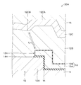
- FIG. 23 is a cross-sectional view showing an example of the configuration of the display device 40 according to the second embodiment of the present disclosure.
- FIG. 24A is a sectional view showing a part of the display device 40 shown in FIG. 23 in an enlarged manner.
- the insulating layer 43 has a plurality of inclined surfaces 43C protruding from the upper surface of the first electrode 12A and surrounding the plurality of first electrodes 12A, respectively.
- the insulating layer 43 has an opening 43H at a portion corresponding to the bottom of the inclined surface 43C.
- the bottom of the insulating layer 43 covers from the peripheral portion of the upper surface of the first electrode 12A to the side surface (end surface) of the first electrode 12A.
- the thickness of the organic layer 12B on the first electrode 12A is substantially constant.
- the opening 43H is provided on the first electrode 12A.
- the peripheral edge of the opening 14H is located inside the peripheral edge of the opening 43H. That is, the first interface layer 14 has the protruding portion 14A that protrudes from the peripheral edge of the opening 43H of the insulating layer 43.
- the protrusion 14A has a substantially uniform thickness, for example.
- the protruding portion 14A may have a tapered shape that increases as the distance from the opening 14H increases.
- the peripheral edge of the opening 14H is located inside the peripheral edge of the opening 43H, when the organic layer 12B is formed by the CVD method or the like, it becomes a shade of the inclined surface 43C and the inside of the lower portion of the inclined surface 43C. It is possible to suppress the thickness of the organic layer 12B from being thinned at a portion. Therefore, the thickness of the organic layer 12B on the first electrode 12A can be made substantially constant. Therefore, it is possible to suppress the occurrence of vertical leakage due to electric field concentration.
- the opening ratio of the insulating layer 43 is preferably higher than that of the first interface layer 14. As a result, the peripheral edge of the opening 43H can be positioned inside the peripheral edge of the opening 13H.
- the opening ratio of the insulating layer 43 is the ratio of the total area of the openings 43H of the insulating layer 43 to the area of the formation region of the insulating layer 43.
- the insulating layer 43 includes a bulk layer 43A that serves as an insulating layer body, and a second interface layer 43B provided at the interface between the bulk layer 43A and the organic layer 12B.
- a second interface layer 43B provided at the interface between the bulk layer 43A and the organic layer 12B.
- the composition of the insulating layer 43 may continuously change from the bulk toward the outermost surface on the organic layer 12B side. Specifically, the oxygen concentration of the insulating layer 43 (more specifically, the concentration of silicon oxide of the insulating layer 43) may be gradually increased from the bulk toward the outermost surface on the organic layer 12B side. The composition of the insulating layer 43 may continuously change from the bulk toward the edge-side surface.
- the fourth embodiment is similar to the third embodiment.
- the thickness of the organic layer 12B on the first electrode 12A is substantially constant. This can prevent the electric field from being concentrated on a part between the first electrode 12A and the second electrode 12C. Therefore, the vertical leakage between the first electrode 12A and the second electrode 12C can be suppressed.
- the insulating layer 43 has a plurality of inclined surfaces 43C surrounding the plurality of first electrodes 12A, respectively. Accordingly, the light emitted from the light emitting element 12 can be reflected by the inclined surface 43C toward the upper side of the first electrode 12A. Therefore, the brightness of the display device 40 can be improved.
- the pixel used in the display device according to the present disclosure described above can be configured to include a resonator structure that resonates the light generated in the light emitting element.
- the resonator structure will be described below with reference to the drawings.
- FIG. 25A is a schematic cross-sectional view for explaining the first example of the resonator structure.
- the light emitting elements 12 provided corresponding to the sub-pixels 100R, 100G, and 100B may be referred to as light emitting elements 12 R , 12 G , and 12 B , respectively.
- the sub-pixel 100R of the organic layer 12B, 100G, portions corresponding to the respective 100B, may be referred to the organic layer 40 R, 40 G, 40 B .
- the first electrode 12A is formed with a common film thickness in each light emitting element 12. The same applies to the second electrode 12C.
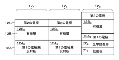
- a reflection plate 71 is arranged below the first electrode 12A of the light emitting element 12 with the optical adjustment layer 72 interposed therebetween.
- a resonator structure that resonates the light generated by the organic layer 12B is formed between the reflector 71 and the second electrode 12C.
- the optical adjustment layers 72 provided corresponding to the sub-pixels 100R, 100G, and 100B may be referred to as optical adjustment layers 72 R , 72 G , and 72 B.
- the reflector 71 is formed to have a common film thickness in each light emitting element 12.
- the film thickness of the optical adjustment layer 72 differs depending on the color to be displayed by the pixel. Since the optical adjustment layers 72 R , 72 G , and 72 B have different film thicknesses, it is possible to set the optical distance that produces the optimum resonance for the wavelength of light according to the color to be displayed.
- the upper surfaces of the reflection plates 71 of the light emitting elements 12 R , 12 G , and 12 B are arranged so as to be aligned.
- the position of the upper surface of the second electrode 12C is the same as that of the light emitting elements 12 R , 12 G , and 12 B. It depends on the type.
- the reflector 71 can be formed using, for example, a metal such as aluminum (Al), silver (Ag), or copper (Cu), or an alloy containing these as the main components.
- the optical adjustment layer 72 is made of an inorganic insulating material such as silicon nitride (SiN x ), silicon oxide (SiO x ), or silicon oxynitride (SiO x N y ), or an organic resin such as an acrylic resin or a polyimide resin. It can be constructed using materials.
- the optical adjustment layer 72 may be a single layer or a laminated film of these plural materials. Further, the number of stacked layers may differ depending on the type of the light emitting element 12.
- the first electrode 12A can be formed using a transparent conductive material such as indium tin oxide (ITO), indium zinc oxide (IZO), or zinc oxide (ZnO).
- ITO indium tin oxide
- IZO indium zinc oxide
- ZnO zinc oxide
- the second electrode 12C needs to function as a semi-transmissive reflective film.
- the second electrode 12C is formed using magnesium (Mg), silver (Ag), or a magnesium-silver alloy (MgAg) containing these as the main components, or an alloy containing an alkali metal or an alkaline earth metal. can do.
- FIG. 25B is a schematic sectional view for explaining the second example of the resonator structure.
- the first electrode 12A and the second electrode 12C are formed to have a common film thickness in each light emitting element 12.
- the reflection plate 71 is arranged below the first electrode 12A of the light emitting element 12 with the optical adjustment layer 72 interposed therebetween.
- a resonator structure that resonates the light generated by the organic layer 12B is formed between the reflector 71 and the second electrode 12C.
- the reflection plate 71 is formed to have a common film thickness in each light emitting element 12, and the film thickness of the optical adjustment layer 72 differs depending on the color to be displayed by the pixel.
- the upper surfaces of the reflection plates 71 of the light emitting elements 12 R , 12 G , and 12 B are arranged so as to be aligned, and the upper surface of the second electrode 12 C is located at the light emitting elements 12 R , 12 B. It was different according to the type of G and 12 B.
- the upper surface of the second electrode 12C is arranged so that the light emitting elements 12 R , 12 G , and 12 B are aligned.
- the upper surface of the reflector 71 in the light emitting element 12 R, 12 G, 12 B are arranged differently depending on the type of light-emitting elements 12 R, 12 G, 12 B ing. Therefore, the lower surface of the reflection plate 71 (in other words, the surface of the base 73 shown by reference numeral 73 in the drawing) has a stepped shape corresponding to the type of the light emitting element 12.
- the materials that form the reflector 71, the optical adjustment layer 72, the first electrode 12A, and the second electrode 12C are the same as those described in the first example, and thus the description thereof is omitted.
- FIG. 26A is a schematic cross-sectional view for explaining the third example of the resonator structure.
- the reflectors 71 provided corresponding to the sub-pixels 100R, 100G, and 100B may be referred to as reflectors 71 R , 71 G , and 71 B.
- the first electrode 12A and the second electrode 12C are formed to have a common film thickness in each light emitting element 12.
- the reflection plate 71 is arranged below the first electrode 12A of the light emitting element 12 with the optical adjustment layer 72 interposed therebetween.
- a resonator structure that resonates the light generated by the organic layer 12B is formed between the reflector 71 and the second electrode 12C.
- the film thickness of the optical adjustment layer 72 differs depending on the color to be displayed by the pixel.
- the positions of the upper surfaces of the second electrodes 12C are arranged so that the light emitting elements 12 R , 12 G , and 12 B are aligned.
- the lower surface of the reflection plate 71 had a stepped shape corresponding to the type of the light emitting element 12 in order to align the upper surfaces of the second electrodes 12C.
- the film thickness of the reflection plate 71 is set to be different depending on the types of the light emitting elements 12 R , 12 G and 12 B. More specifically, the film thickness is set so that the lower surfaces of the reflectors 71 R , 71 G and 71 B are aligned.
- the materials that form the reflector 71, the optical adjustment layer 72, the first electrode 12A, and the second electrode 12C are the same as those described in the first example, and thus the description thereof is omitted.
- FIG. 26B is a schematic sectional view for explaining the fourth example of the resonator structure.
- the first electrodes 12A provided corresponding to the sub-pixels 100R, 100G, 100B may be referred to as first electrodes 12A R , 12A G , 12A B.
- the first electrode 12A and the second electrode 12C of each light emitting element 12 are formed with a common film thickness. Then, the reflection plate 71 is disposed below the first electrode 12A of the light emitting element 12 with the optical adjustment layer 72 interposed therebetween.
- the optical adjustment layer 72 is omitted, and the film thickness of the first electrode 12A is set to be different depending on the types of the light emitting elements 12 R , 12 G , and 12 B. did.
- the reflector 71 is formed to have a common film thickness in each light emitting element 12.
- the film thickness of the first electrode 12A differs depending on the color to be displayed by the pixel. Since the first electrodes 12A R , 12A G , and 12A B have different film thicknesses, it is possible to set the optical distance that produces the optimum resonance for the wavelength of light according to the color to be displayed.
- the materials that form the reflector 71, the optical adjustment layer 72, the first electrode 12A, and the second electrode 12C are the same as those described in the first example, and thus the description thereof is omitted.
- FIG. 27A is a schematic cross-sectional view for explaining the fifth example of the resonator structure.
- the first electrode 12A and the second electrode 12C are formed with a common film thickness in each light emitting element 12. Then, the reflection plate 71 is disposed below the first electrode 12A of the light emitting element 12 with the optical adjustment layer 72 interposed therebetween.
- the optical adjustment layer 72 was omitted, and instead, the oxide film 74 was formed on the surface of the reflection plate 71.
- the thickness of the oxide film 74 was set to be different depending on the types of the light emitting elements 12 R , 12 G and 12 B.
- the oxide films 74 provided corresponding to the sub-pixels 100R, 100G, and 100B may be referred to as oxide films 74 R , 74 G , and 74 B.
- the film thickness of the oxide film 74 differs depending on the color to be displayed by the pixel. Since the oxide films 74 R , 74 G , and 74 B have different film thicknesses, it is possible to set the optical distance that produces the optimum resonance for the wavelength of light according to the color to be displayed.
- the oxide film 74 is a film obtained by oxidizing the surface of the reflection plate 71, and is made of, for example, aluminum oxide, tantalum oxide, titanium oxide, magnesium oxide, zirconium oxide, or the like.
- the oxide film 74 functions as an insulating film for adjusting the optical path length (optical distance) between the reflection plate 71 and the second electrode 12C.
- the oxide film 74 having a different film thickness depending on the types of the light emitting elements 12 R , 12 G , and 12 B can be formed, for example, as follows.
- the container is filled with the electrolytic solution, and the substrate on which the reflection plate 71 is formed is immersed in the electrolytic solution. Further, the electrodes are arranged so as to face the reflection plate 71.
- a positive voltage is applied to the reflection plate 71 with the electrode as a reference to anodize the reflection plate 71.
- the thickness of the oxide film formed by anodic oxidation is proportional to the voltage value applied to the electrodes. Therefore, anodization is performed in a state in which a voltage according to the type of the light emitting element 12 is applied to each of the reflection plates 71 R , 71 G , and 71 B. Thereby, the oxide films 74 having different film thicknesses can be collectively formed.
- the materials and the like that form the reflector 71, the first electrode 12A, and the second electrode 12C are the same as those described in the first example, so description will be omitted.
- FIG. 27B is a schematic sectional view for explaining the sixth example of the resonator structure.
- the light emitting element 12 is configured by laminating a first electrode 12A, an organic layer 12B, and a second electrode 12C.
- the first electrode 12A is formed to have the functions of both the electrode and the reflector.
- the first electrode (and reflective plate) 12A is formed of a material having optical constants that are selected depending on the type of light-emitting elements 12 R, 12 G, 12 B . Since the phase shift due to the first electrode (also serving as the reflection plate) 12A is different, it is possible to set the optical distance that produces the optimum resonance for the wavelength of light according to the color to be displayed.
- the first electrode (also reflective plate) 12A can be made of a single metal such as aluminum (Al), silver (Ag), gold (Au), or copper (Cu), or an alloy containing these as main components. ..
- the first electrode (and reflective plate) of the light emitting element 12 R and 12A R is formed of copper (Cu)
- the first electrode (and reflective plate) 12A G of the light-emitting element 12 G of the light-emitting element 12 B first electrode (and reflective plate) and 12A B may be configured such forms of aluminum.
- the materials and the like that make up the second electrode 12C are the same as the contents described in the first example, so description will be omitted.
- FIG. 28 is a schematic cross-sectional view for explaining the seventh example of the resonator structure.
- the seventh example is basically a configuration in which the sixth example is applied to the light emitting elements 12 R and 12 G and the first example is applied to the light emitting element 12 B. Also in this configuration, it is possible to set the optical distance that produces the optimum resonance for the wavelength of light according to the color to be displayed.
- the first electrodes (also reflecting plates) 12A R and 12A G used for the light emitting elements 12 R and 12 G are single metals such as aluminum (Al), silver (Ag), gold (Au), and copper (Cu). , And can be composed of an alloy containing these as main components.
- the display device according to any of the above-described first embodiment and its modification is incorporated in various electronic devices as a module as shown in FIG. 29, for example.
- the display device according to any of the second to fourth embodiments and the modifications thereof may be incorporated in various electronic devices as a module as shown in FIG. 29, for example.
- high resolution is required for an electronic viewfinder of a video camera or a single-lens reflex camera, a head-mounted display, or the like, and it is suitable for those used by enlarging it near the eyes.
- This module has a region 210 on one short side of the substrate 11 that is exposed without being covered by the counter substrate 18 and the filling resin layer 17, and in this region 210, the signal line driving circuit 120 and the scanning line driving circuit 130.
- An external connection terminal (not shown) is formed by extending the wiring of FIG.
- a flexible printed circuit (FPC) 220 for inputting and outputting signals may be connected to the external connection terminals.
- 30A and 30B show an example of the external appearance of the digital still camera 310.
- This digital still camera 310 is of an interchangeable lens type single-lens reflex type, and has an interchangeable taking lens unit (interchangeable lens) 312 substantially in the center of the front of a camera body (camera body) 311 and a front left side. It has a grip portion 313 for the photographer to hold.
- interchangeable lens unit interchangeable lens
- a monitor 314 is provided at a position displaced from the center of the rear surface of the camera body 311 to the left.
- An electronic viewfinder (eyepiece window) 315 is provided above the monitor 314. By looking through the electronic viewfinder 315, the photographer can visually recognize the optical image of the subject guided from the photographing lens unit 312 and determine the composition.
- the display device according to any of the above-described first embodiment and its modification can be used. Further, as the electronic viewfinder 315, it is possible to use the display device according to any one of the above-described second to fourth embodiments and their modifications.
- FIG. 31 shows an example of the external appearance of the head mounted display 320.
- the head-mounted display 320 has, for example, ear hooks 322 to be worn on the head of the user, on both sides of the eyeglass-shaped display 321.
- the display unit 321 the display device according to any of the above-described first embodiment and its modification can be used. Further, as the display unit 321, it is also possible to use the display device according to any of the above-described second to fourth embodiments and their modifications.
- FIG. 32 shows an example of the appearance of the television device 330.
- the television device 330 has, for example, a video display screen section 331 including a front panel 332 and a filter glass 333, and the video display screen section 331 is one of the above-described first embodiment and its modification. It is composed of a display device according to Kani. Further, the video display screen section 331 may be configured by the display device according to any of the above-described second to fourth embodiments and their modifications.
- FIG. 33 shows an example of the appearance of a stand-type lighting device 400.
- a lighting unit 413 is attached to a column 412 provided on a base 411.
- the illuminating section 413 in the display device according to any of the above-described first embodiment and its modification, or the display device according to any of the above-described second to fourth embodiments and their modifications.
- the drive circuits for the display device such as the signal line drive circuit 120 and the scanning line drive circuit 130, those provided with a drive circuit for the illumination device are used.
- the color filter 16 may be omitted, and the size of the opening of the insulating layer 13 may be appropriately selected according to the optical characteristics of the lighting device 400.
- the substrate 11 and the counter substrate 18 by using a film as the substrate 11 and the counter substrate 18 and having a flexible structure, it is possible to have an arbitrary shape such as the cylindrical shape or the curved surface shape shown in FIG.
- the number of light emitting elements 12 may be singular.
- a monochromatic filter may be provided instead of the color filter 16.
- the form of the lighting device is not limited to this, and may be, for example, a form installed on a ceiling, a wall, or a floor. It may be.
- the average thickness of the first interface layer and the second interface layer, the peak intensity ratio of the bulk layer (I NH /I Si-H 2) and the silicon oxide contained in the second interface layer The ratio of silicon oxide to the total amount of silicon nitride is the value obtained by the measuring method described in the first embodiment.
- a driving circuit and the like were formed on one main surface of a silicon substrate by using a thin film forming technique, a photolithography technique, and an etching technique.
- a metal layer is formed over a driver circuit or the like by a sputtering method, and then the metal layer is patterned by using a photolithography technique and an etching technique so that each light-emitting element (that is, each subpixel) is separated.
- a plurality of first electrodes was formed.
- a first interface layer (SiO layer) having an average thickness of 5 nm is formed on one main surface of the silicon substrate on which the plurality of first electrodes are formed by the plasma CVD method, and then the average thickness is formed by the CVD method.
- a 40 nm bulk layer (SiN layer) was formed.
- SiH 4 , NH 2 and NH 3 were used as process gases.
- the mixing ratio of the process gas bulk layers having different composition ratios were formed in Examples 1-1 and 1-2.
- the absorption spectrum of the bulk layer was measured by FT-IR. The results are shown in FIGS. 34A and 34B.
- the first interface layer and the bulk layer were patterned by using photolithography technology and etching technology. Then, the surface of the bulk layer was subjected to plasma treatment to form a second interface layer (SiON layer) of 3 nm on the surface of the bulk layer to obtain an insulating layer. At this time, the conditions of the plasma treatment were adjusted so that the ratio of silicon oxide to the total amount of silicon oxide and silicon nitride contained in the second interface layer was 90%.
- an organic layer was formed by stacking a hole injection layer, a hole transport layer, a light emitting layer, and an electron transport layer on the first electrode and the insulating layer in this order by vapor deposition.
- the second electrode was formed on the organic layer by the sputtering method. As a result, a plurality of light emitting elements were formed on the one main surface of the silicon substrate.
- a protective layer was formed on the second electrode by the CVD method, and then a color filter was formed on the protective layer.
- the counter substrate was placed on the filling resin layer.
- the filled resin layer was irradiated with ultraviolet rays to cure the filled resin layer, so that the substrate and the counter substrate were bonded together via the filled resin layer. As a result, the display device was sealed.
- the leak current between pixels of the display devices of Examples 1-1 and 1-2 obtained as described above was measured.
- the inter-pixel leak current was measured by measuring the current values flowing in the R and G sub-pixels with respect to the voltage applied to the B sub-pixel among the RGB sub-pixels.
- the evaluation of the leak amount between pixels, which will be described later, was also performed by the same measurement. As a result of the above measurement, it was found that the interpixel leak current depends on the peak intensity ratio (I NH /I Si-H ) of the bulk layer.
- Example 1-1 in which the peak intensity ratio (I NH /I Si-H ) was 0.45, in Example 1-1 in which the peak intensity ratio (I NH /I Si-H ) was 4.96. It was found that the leak current flowing between pixels was suppressed as compared with 1-2.
- the interpixel leakage current depends on the peak intensity ratio (I NH /I Si-H ) of the bulk layer, and the interpixel leakage current is suppressed as the peak intensity ratio (I NH /I Si-H ) becomes smaller. ..
- the peak intensity ratio (I NH /I Si-H ) is preferably less than 4, and more preferably 3 or less.
- Example 3-1 to 3-6 The average thickness of the first interface layer is 1 nm (Example 3-1), 3 nm (Example 3-2), 7 nm (Example 3-3), 9 nm (Example 3-4), 11 nm (Example 3). -5), 13 nm (Example 3-6), and 15 nm (Example 3-7) except that the display device was manufactured in the same manner as in Example 1-1 (average thickness of the first interface layer: 5 nm). Obtained.
- Example 3-1 A display device was obtained in the same manner as in Example 1-1, except that the first interface layer was not formed.
- the interpixel leakage current depends on the average thickness of the first interface.
- the average thickness of the first interface layer is preferably 1 nm or more and less than 15 nm, more preferably 1 nm or more and 13 nm or less, still more preferably 1 nm or more and 9 nm or less, and particularly preferably 1 nm or more. It is 7 nm or less, and most preferably 1 nm or more and 5 nm or less.
- the leak current between pixels increases because the fixed charge in the bulk layer decreases due to the reaction between the first electrode and the bulk layer. It is considered that it is impossible to maintain the positively charged state.
- the average thickness of the first interface layer is 15 nm or more, the inter-pixel leakage current increases because the hole current flows from the first electrode to the upper surface of the insulating layer along the edge of the first interface layer. It is thought that this is because the flow becomes easier.
- the leak current between pixels of the display devices of Examples 4-1 to 4-3 obtained as described above was measured.
- the interpixel leakage current depends on the ratio of silicon oxide to the total amount of silicon oxide and silicon nitride contained in the second interface layer, and from the viewpoint of suppressing the interpixel leakage current, the ratio is set to 80% or more. It turned out that it is preferable to do.
- Example 5-1 a display device having the configuration shown in FIG. 11 was manufactured as follows. First, a thin film forming technique, a photolithography technique, and an etching technique were used to obtain a silicon substrate on which a driving circuit and the like were formed on one main surface, as shown in FIG. 15A. Next, as shown in FIG. 15B, an electrode layer (ACX/ITO layer) is formed on the drive circuit or the like by a sputtering method, and then the electrode layer is patterned by using a photolithography technique and an etching technique. As shown in FIG. 15C, a plurality of first electrodes separated for each light emitting element (that is, for each subpixel) were formed.
- a first interface layer (SiO layer) is formed on one main surface of the silicon substrate on which a plurality of first electrodes are formed by a CVD method, and then an etchback method is performed.
- the first interface layer 24 was removed so that the first interface layer having the same height as the first electrode 12A remained on the side surface of the first electrode.
- a bulk layer (SiN layer) was formed by the CVD method as shown in FIG. 15F.
- a photoresist layer was formed on the bulk layer by spin coating, and the surface was flattened.
- the photoresist layer is removed and a part of the bulk layer is removed by an etch-back method to remove the first electrode, the first interface layer, and the bulk having the same height. Layers were formed.
- the surface of the bulk layer 13A was plasma-treated to form a second interface layer (SiON layer) having an average thickness of 2.5 nm. As a result, an insulating layer was obtained.
- the hole injection layer, the hole transport layer, the light emitting layer, and the electron transport layer were laminated in this order on the first electrode, the first interface layer, and the insulating layer by the vapor deposition method. As a result, an organic layer having a constant organic layer thickness was formed.
- the subsequent steps were performed in the same manner as in Example 1-1 to obtain a display device.
- the average thickness of the first electrode, the first interface layer, and the insulating layer was set to 65 nm by adjusting the process conditions.
- Example 5-2 a display device having the configuration shown in FIG. 14 was manufactured as follows. That is, a display device was produced in the same manner as in Example 1 except that the average thickness of the insulating layer was adjusted to 85 nm by adjusting the process conditions.
- Example 5-3 a display device having the configuration shown in FIG. 18 was manufactured as follows. First, the steps from the substrate forming step to the first interface layer forming step are performed in the same manner as in Example 5-1, and as shown in FIG. 20A, on the main surface of the substrate on which the plurality of first electrodes are formed. Then, a first interface layer (SiO layer) was formed.
- a first interface layer SiO layer
- a bulk layer (SiN layer) was formed on the first interface layer by the CVD method.
- a photoresist layer was formed on the bulk layer, and then an opening was formed in a portion of the photoresist layer corresponding to the first electrode.
- an opening was formed by etching in a portion of the first interface layer and the bulk layer corresponding to the first electrode layer.
- etching was performed by using a deposition gas such as CH 2 F 2 to adjust the etching rates of the first interface layer (SiO) and the bulk layer (SiN).
- the surface of the bulk layer 13A was plasma-treated to form a second interface layer (SiON layer) having an average thickness of 2.5 nm.
- a second interface layer SiON layer
- a hole injection layer, a hole transport layer, a light emitting layer, and an electron transport layer were laminated in this order on the first electrode and the insulating layer by a vapor deposition method.
- FIG. 21C an organic layer having a plurality of convex portions on the upper surface and having a substantially constant thickness of the organic layer in the region inside the convex portions was formed.
- the subsequent steps were performed in the same manner as in Example 1-1 to obtain a display device.
- the average thickness of the first electrode was set to 65 nm
- the average thickness of the first interface layer was set to 9 nm
- the average thickness of the insulating layer was set to 26 nm.
- Example 5-4 a display device having the configuration shown in FIG. 19 was manufactured as follows. In the step of forming the opening of the first interface layer and the bulk layer, the first interface layer (SiO) and the bulk layer (SiN) are arranged so that the peripheral edge of the opening of the insulating layer and the peripheral edge of the opening of the first interface layer overlap. A display device was obtained in the same manner as in Example 5-1 except that the etching rate of () was adjusted.
- Comparative Example 5-1 a display device having the configuration shown in FIG. 13 was manufactured as follows. That is, a display device was produced in the same manner as in Example 1 except that the average thickness of the insulating layer was adjusted to 45 nm by adjusting the process conditions.
- the luminous efficiency of the display devices of Examples 5-1 to 5-3 is higher than that of the display devices of Example 5-4 and Comparative example 5-1. Especially, the luminous efficiency is high in a low current density region.
- Example 6-1 a display device having the configuration shown in FIG. 38A was set as a model for electromagnetic field simulation. The setting conditions for each layer are shown below.
- First electrode Al electrode
- the current density distribution of the organic layer was calculated by electromagnetic field simulation (ANSYS Maxwell) using the above model. The results are shown in FIGS. 40 and 41.
- the integrated value of the portion indicated by the straight line L (length 10 nm) in FIG. 41 was 1.29 ⁇ 10 ⁇ 6 A/m.
- Numerals (1), (2), (3), etc. in FIGS. 40 and 41 respectively correspond to the magnitude of the current density (gradation in the legend). Also in the figures showing the simulation results of Example 6-2 and Comparative examples 6-1 and 6-2 below, the symbols (1), (2), (3), etc. similarly indicate the magnitude of the current density ( Corresponding to the gradation of the legend).
- Example 6-1 a display device having the configuration shown in FIG. 38B was set as a model for electromagnetic field simulation. The setting conditions for each layer are shown below.
- First electrode Al electrode
- the current density distribution of the organic layer was calculated by electromagnetic field simulation (ANSYS Maxwell) using the above model. The results are shown in FIGS. 42 and 43.
- the integrated value of the portion indicated by the straight line L (length 10 nm) in FIG. 43 was 1.48 ⁇ 10 ⁇ 6 A/m.
- the upper limit value or the lower limit value of the numerical range of a certain stage is the upper limit of the numerical range of another stage. You may replace with a value or a lower limit.
- a plurality of first electrodes provided for each pixel An insulating layer provided between the first electrodes and covering a peripheral portion of the first electrodes, the insulating layer containing a silicon compound; A first interface layer provided at an interface between the first electrode and the insulating layer, the first interface layer including a first silicon oxide; An organic layer provided on the first electrode and the insulating layer in common to all pixels and including a light emitting layer; A second electrode provided on the organic layer,
- the said insulating layer is a display device containing the 2nd silicon oxide in the surface part by the side of the said organic layer.
- the silicon compound includes silicon nitride, The display device according to (2), wherein the ratio of the second silicon oxide to the total amount of the second silicon oxide and the silicon nitride contained in the surface portion on the organic layer side is 80% or more.
- the insulating layer is A bulk layer containing the silicon compound, The display device according to any one of (1) to (3), further comprising: a second interface layer that is provided at an interface between the bulk layer and the organic layer and that includes the second silicon oxide. (6) The display device according to (5), wherein the average thickness of the second interface layer is 10 nm or less. (7) The second interface layer is composed of two or more layers, The display device according to (5) or (6), wherein at least one layer of the two or more layers contains the second silicon oxide. (8) The second interface layer is A first layer comprising the second silicon oxide; A second layer provided on the first layer, the second layer containing at least one of silicon nitride and silicon oxynitride, (5) or (6).
- the display device according to any one of (5) to (8), further including an intermediate layer provided between the second interface layer and the bulk layer and containing silicon fluoride.
- the display device according to any one of (5) to (9), wherein the second interface layer covers the main surface of the bulk layer and the edge of the bulk layer.
- the portion of the second interface layer that covers the edge of the bulk layer has a different composition from the portion of the second interface layer that covers the main surface of the bulk layer.
- (12) The display device according to (11), wherein a portion of the second interface layer that covers an edge of the insulating layer is positively charged.
- the average thickness of the first interface layer is less than 15 nm.
- the display device according to any one of (1) to (13), wherein the insulating layer is positively charged.
- the silicon compound contains silicon nitride.
- the insulating layer further comprises hydrogen, The peak intensity ratio NH between the NH bond-derived peak intensity I NH and the Si—H bond-derived peak intensity I Si-H (I NH obtained by analyzing the insulating layer by X-ray photoelectron spectroscopy) /I Si-H ) is less than 4, the display device according to (15).
- the first electrode includes an oxide conductive layer.
- the organic layer has a plurality of convex portions provided on portions of the surface on the second electrode side corresponding to the peripheral portions of the plurality of first electrodes, The display device according to any one of (1) to (17), wherein the thickness of the organic layer in the region inside the convex portion is substantially constant.
- the first interface layer has a plurality of first openings respectively provided on the plurality of first electrodes
- the insulating layer has a plurality of second openings respectively provided on the plurality of first electrodes
- the display device according to (18) wherein the aperture ratio of the insulating layer is higher than the aperture ratio of the first interface layer.
- the first interface layer has a plurality of first openings respectively provided on the plurality of first electrodes,
- the insulating layer has a plurality of second openings respectively provided on the plurality of first electrodes,
- the display device according to (18) or (19) wherein the peripheral edge of the first opening is located inside the peripheral edge of the second opening.
- the first interface layer has a protrusion that protrudes with respect to the peripheral edge of the second opening,
- the display device according to (20) wherein the thickness of the protrusion increases with increasing distance from the first opening.
- the display device according to any one of (1) to (22), wherein the pixel includes a resonator structure that resonates light generated by a light emitting element.
- An electronic device comprising the display device according to any one of (1) to (23).
- a plurality of first electrodes provided for each pixel, An insulating layer provided between the first electrodes and containing a silicon compound;
- a first interface layer provided between a side surface of the first electrode and a side surface of the insulating layer, the first interface layer including a first silicon oxide;
- An organic layer provided on the first electrode and the insulating layer in common to all pixels and including a light emitting layer;
- a second electrode provided on the organic layer, A display device in which the thickness of the organic layer on the first electrode is substantially constant.
- the height H 1 of the organic layer on the first electrode and the height H 2 of the organic layer in the peripheral portion of the first electrode satisfy the relationship of H 1 ⁇ H 2 (24).
- the height h 1 of the first electrode, the height h 2 of the first interface layer and the height h 3 of the insulating layer satisfy the relationship of h 1 ⁇ h 2 ⁇ h 3 (25) or ( 26) The display device according to 26).
- the first interface layer has a plurality of first openings provided corresponding to each of the plurality of first electrodes
- the insulating layer has a plurality of second openings provided corresponding to the plurality of first electrodes, respectively.
- the insulating layer contains second silicon oxide on a surface portion on the organic layer side.
- An electronic apparatus comprising the display device according to any one of (25) to (35).
Landscapes
- Physics & Mathematics (AREA)
- Optics & Photonics (AREA)
- Engineering & Computer Science (AREA)
- Microelectronics & Electronic Packaging (AREA)
- Geometry (AREA)
- Electroluminescent Light Sources (AREA)
- Devices For Indicating Variable Information By Combining Individual Elements (AREA)
Abstract
Description
1 第1の実施形態
1-1 表示装置の構成
1-2 表示装置の製造方法
1-3 効果
1-4 変形例
2 第2の実施形態
2-1 表示装置の構成
2-2 表示装置の製造方法
2-3 効果
2-4 変形例
3 第3の実施形態
3-1 表示装置の構成
3-2 表示装置の製造方法
3-3 効果
4 第4の実施形態
4-1 表示装置の構成
4-2 効果
5 各実施形態に適用される共振器構造の例
6 応用例
図1は、本開示の第1の実施形態に係る有機EL(Electro-Luminescence)表示装置10(以下、単に「表示装置10」という。)の全体構成の一例を示す。表示装置10は、各種の電子機器に用いて好適なものであり、基板11上には表示領域110Aおよび表示領域110Aの周縁に周辺領域110Bが設けられている。表示領域110A内には、複数のサブ画素100R、100G、100Bがマトリクス状に配置されている。サブ画素100Rは赤色を表示し、サブ画素100Gは緑色を表示し、サブ画素100Bは青色を表示する。なお、以下の説明において、サブ画素100R、100G、100Bを特に区別しない場合には、サブ画素100という。
第1の電極12Aは、サブ画素100R、100G、100B毎に電気的に分離して設けられている。第1の電極12Aは、反射層としての機能も兼ねており、できるだけ反射率が高く、かつ仕事関数が大きい金属層によって構成されることが、発光効率を高める上で好ましい。金属層の構成材料としては、例えば、クロム(Cr)、金(Au)、白金(Pt)、ニッケル(Ni)、銅(Cu)、モリブデン(Mo)、チタン(Ti)、タンタル(Ta)、アルミニウム(Al)、マグネシウム(Mg)、鉄(Fe)、タングステン(W)、銀(Ag)等の金属元素の単体および合金のうちの少なくとも1種を用いることができる。合金の具体例としては、AlNi合金、AlCu合金等が挙げられる。第1の電極12Aが、上記の金属元素の単体および合金のうちの少なくとも1種を含む複数の金属層の積層膜により構成されていてもよい。
第2の電極12Cは、表示領域110A内においてすべてのサブ画素100R、100G、100Bに共通の電極として設けられている。第2の電極12Cは、有機層12Bで発生した光に対して透過性を有する透明電極である。ここで、透明電極には、半透過性反射膜も含まれるものとする。第2の電極12Cは、例えば、金属または金属酸化物により構成される。金属としては、例えば、アルミニウム(Al)、マグネシウム(Mg)、カルシウム(Ca)、ナトリウム(Na)等の金属元素の単体および合金のうちの少なくとも1種を用いることができる。合金としては、例えば、マグネシウム(Mg)と銀(Ag)との合金(MgAg合金)、またはアルミニウム(Al)とリチウム(Li)との合金(AlLi合金)が好適である。金属酸化物としては、例えば、インジウム酸化物と錫酸化物の混合体(ITO)、インジウム酸化物と亜鉛酸化物の混合体(IZO)または酸化亜鉛(ZnO)等の金属酸化物を用いることができる。
絶縁層13は、第1の電極12Aをサブ画素100R、100G、100B毎に電気的に分離するためのものである。絶縁層13は、第1の電極12Aの間に設けられると共に、第1の電極12Aの周縁部を覆っている。より具体的には、絶縁層13は、各第1の電極12Aに対応する部分に開口を有しており、第1の電極12Aの上面(第2の電極12Cとの対向面)の周縁部から第1の電極12Aの側面(端面)にかけて覆っている。第1の電極12Aと絶縁層13の界面には、第1の界面層14が設けられている。
バルク層13Aは、正に帯電していることが好ましい。バルク層13Aが正に帯電していることで、隣接する発光素子12間で生じる正孔電流のリークを抑制することができる。
第2の界面層13Bは、隣接する発光素子12間で生じる正孔電流のリークおよび電子電流のリークを抑制するためのものである。第2の界面層13Bは、格子歪みを有しており、これにより、上述の正孔電流のリークおよび電子電流のリークの抑制機能が発現する。ここで、“格子歪み”とは、第2の界面層13B中に含まれる微小な結晶粒の格子歪みも含まれるものとする。本明細書において、“正孔電流のリーク”とは、アノードである第1の電極12Aから注入された正孔が絶縁層13と有機層12Bの界面を伝って、隣接する第1の電極12Aに流れる現象のことをいう。また、“電子電流のリーク”とは、カソードである第2の電極12Cからから注入された電子が有機層12Bを伝って、隣接する第1の電極12Aに流れる現象、または有機層12Bが含む電荷生成層(例えば正孔注入層)で形成された電子が、有機層12Bを伝って流れる現象のことをいう。
第1の界面層14は、第1の電極12Aと絶縁層13との膜を構成する要素のやり取り、例えば酸素のやり取りを抑制し、絶縁層13の特性の劣化を抑制するためのものである。具体的には例えば、バルク層13Aの固定電荷の減少を抑制し、絶縁層13(具体的にはバルク層13A)が正に帯電した状態を保持するためのものである。
有機層12Bは、表示領域110A内においてすべてのサブ画素100R、100G、100Bに共通の有機層として設けられている。図4は、図2に示した有機層12Bを拡大して表す。有機層12Bは、第1の電極12Aの側から正孔注入層12B1、正孔輸送層12B2、発光層12B3、電子輸送層12B4がこの順序で積層された構成を有する。なお、有機層12Bの構成はこれに限定されるものではなく、発光層12B3以外の層は必要に応じて設けられるものである。
保護層15は、発光素子12を外気と遮断し、外部環境から発光素子12内部への水分浸入を抑制するためのものである。また、第2の電極12Cが金属層により構成されている場合には、保護層15は、この金属層の酸化を抑制する機能も有している。
カラーフィルタ16は、いわゆるオンチップカラーフィルタ(On Chip Color Filter:OCCF)である。カラーフィルタ16は、例えば、赤色フィルタ16R、緑色フィルタ16Gおよび青色フィルタ16Bを備える。赤色フィルタ16R、緑色フィルタ16G、青色フィルタ16Bはそれぞれ、サブ画素100Rの発光素子12、サブ画素100Gの発光素子12、サブ画素100Bの発光素子12に対向して設けられている。これにより、サブ画素100R、サブ画素100G、サブ画素100B内の各発光素子12から発せられた白色光がそれぞれ、上記の赤色フィルタ16R、緑色フィルタ16Gおよび青色フィルタ16Bを透過することによって、赤色光、緑色光、青色光がそれぞれ表示面から出射される。また、各色のカラーフィルタ間、すなわちサブ画素100間の領域には、遮光層16BMが設けられている。
充填樹脂層17は、保護層15とカラーフィルタ16との間の空間に充填されている。充填樹脂層17は、カラーフィルタ16と対向基板18とを接着する接着層としての機能を有している。充填樹脂層17は、熱硬化型樹脂および紫外線硬化型樹脂のうちの少なくとも1種の樹脂材料により構成される。
対向基板18は、対向基板18の一主面と、複数の発光素子12が設けられた基板11の一主面とが対向するように設けられている。対向基板18は、充填樹脂層17と共に、発光素子12およびカラーフィルタ16等を封止するものである。対向基板18は、カラーフィルタ16からから出射される各色光に対して透明なガラス等の材料により構成される。
以下、上述の構成を有する表示装置10の製造方法について説明する。
まず、例えば薄膜形成技術、フォトリソグラフィ技術およびエッチング技術を用いて、基板11の一主面に駆動回路等を形成する。次に、例えばスパッタリング法により、金属層を駆動回路等の上に形成したのち、例えばフォトリソグラフィ技術およびエッチング技術を用いて金属層をパターニングすることにより、発光素子12毎(すなわちサブ画素100毎)に分離された複数の第1の電極12Aを形成する。
上述したように、第1の実施形態に係る表示装置10は、サブ画素100毎に設けられた複数の第1の電極12Aと、第1の電極12A間に設けられると共に第1の電極12Aの周縁部を覆う、ケイ素化合物を含む絶縁層13と、第1の電極12Aと絶縁層13の界面に設けられ、酸化ケイ素を含む第1の界面層14と、第1の電極12Aおよび絶縁層13上に全画素に共通して設けられ、発光層12B3を含む有機層12Bと、有機層12B上に設けられた第2の電極12Cとを備える。また、絶縁層13は、ケイ素化合物を主成分として含むバルク層13Aと、バルク層13Aと有機層12Bの界面に設けられ、酸化ケイ素を含む第2の界面層13Bとを備える。これにより、有機層12Bおよび絶縁層13の界面を伝う正孔電流および電子電流を抑制することができる。したがって、表示装置10の電流発光効率の低下および発光色異常等を抑制することができる。
(変形例1)
図5は、本開示の第1の実施形態の変形例1に係る表示装置101の構成の一例を示す。表示装置101は、絶縁層13に代えて、絶縁層131を備える点において、第1の実施形態に係る表示装置10と異なっている。絶縁層131は、バルク層13Aと、第2の界面層13Bと、バルク層13Aおよび第2の界面層13Bの間に設けられた中間層13Cとを備える。
図6は、本開示の第1の実施形態の変形例2に係る表示装置102の構成の一例を示す。表示装置102は、絶縁層13に代えて、絶縁層132を備える点において、第1の実施形態に係る表示装置10と異なっている。絶縁層132は、バルク層13Aと、バルク層13A上に設けられた2層構造の第2の界面層13Dを備える。
図7は、本開示の第1の実施形態の変形例3に係る表示装置103の構成の一例を示す。表示装置103は、絶縁層13に代えて、絶縁層133を備える点において、第1の実施形態に係る表示装置10と異なっている。
図8は、本開示の第1の実施形態の変形例4に係る表示装置104の構成の一例を示す。表示装置104は、バルク層13Aと第2の界面層13Bとを備える絶縁層13に代えて、単層の絶縁層134を備える点において、第1の実施形態に係る表示装置10と異なっている。
図9は、本開示の第1の実施形態の変形例5に係る表示装置105の構成の一例を示す。表示装置105は、単層構造の第1の電極12Aに代えて、積層構造の第1の電極12Dを備える点において、第1の実施形態に係る表示装置10と異なっている。
[2-1 表示装置の構成]
図10は、本開示の第2の実施形態に係る表示装置20の構成の一例を示す断面図である。図11は、図10に示した表示装置20の一部を拡大して表す断面図である。表示装置20は、絶縁層13および第1の界面層14に代えて、絶縁層23および第1の界面層24を備える点において、第1の実施形態に係る表示装置10とは異なっている。
絶縁層23は、第1の電極12Aをサブ画素100R、100G、100B毎に電気的に分離するためのものである。絶縁層23は、基板11の面内方向に隣接する第1の電極12Aの側面間に設けられている。絶縁層23の上面は、平坦になっている。本明細書において、“上面”とは、表示装置20の表示面側となる面のことをいう。
第1の界面層24は、絶縁層23の側面と第1の電極12Aの側面の間に設けられている。第1の界面層24の上面は、平坦になっている。第1の界面層24において、上記以外のことは、第1の実施形態における第1の界面層14と同様である。
第1の電極12A上における有機層12Bの厚みが、ほぼ一定である。すなわち、第1の電極12A上における有機層12Bの上面が、ほぼ平坦となっている。これにより、第1の電極12Aと第2の電極12C(具体的には、第2の電極12Cのうち第1の電極12A上に対応する部分)との間の縦方向リーク(図11中の矢印I1参照)を抑制することができる。これに対して、図12に示すように、有機層12Bの上面のうち第1の電極12Aの周縁部に対応する部分に凹部12BAが形成され、第1の電極12A上における有機層12Bの厚みが、ほぼ一定でない表示装置(すなわち、第1の電極12A上における有機層12Bの上面が、ほぼ平坦でない表示装置)20Aでは、第1の電極12Aと第2の電極12Cの間の一部に電界が集中する。これにより、第1の電極12Aと第2の電極12C(具体的には、第2の電極12Cのうち第1の電極12A上に対応する部分)との間の縦方向リーク(図11中の矢印I1参照)が大きくなる。本明細書において、“縦方向リーク”とは、有機層12Bの厚み方向における、第1の電極12Aと第2の電極12Cとの間の正孔電流リークおよび電子電流リークのことをいう。
第1の電極12A上における有機層12Bの高さH1、および第1の電極12Aの周囲の部分における有機層12Bの高さH2が、H1≦H2の関係を満たす。これにより、第1の電極12Aと第2の電極12Cの間の一部に電界が集中することを抑制することができる。したがって、第1の電極12Aと第2の電極12C(具体的には、第2の電極12Cのうち、第1の電極12Aの周囲の部分に対応する部分)の間の縦方向リーク(図11中の矢印I2参照)を抑制することができる。これに対して、図13に示すように、第1の電極12A上における有機層12Bの高さH1、および第1の電極12Aの周囲の部分における有機層12Bの高さH2が、H1≦H2の関係を満たさない表示装置20Bでは、第1の電極12Aと第2の電極12Cの間の一部に電界が集中する。これにより、第1の電極12Aと第2の電極12C(具体的には、第2の電極12Cのうち、第1の電極12Aの周囲の部分に対応する部分)との間の縦方向リーク(図13中の矢印I2参照)が大きくなる。本明細書において、“第1の電極12Aの周囲の部分”とは、第1の電極12Aの側面から50nm以下の範囲を意味する。
以下、上述の構成を有する表示装置20の製造方法について説明する。
まず、例えば薄膜形成技術、フォトリソグラフィ技術およびエッチング技術を用いて、図15Aに示すように、駆動回路等を含む基板11を形成する。次に、例えばスパッタリング法により、図15Bに示すように、金属層または金属酸化物層等の電極層12A1を基板11上に形成したのち、例えばフォトリソグラフィ技術およびエッチング技術を用いて電極層12A1をパターニングすることにより、図15Cに示すように、発光素子12毎(すなわちサブ画素100毎)に分離された複数の第1の電極12Aを形成する。
上述したように、第2の実施形態に係る表示装置20では、第1の電極12A上における有機層12Bの厚みが、ほぼ一定であり、かつ、第1の電極12A上における有機層12Bの高さh1、および第1の電極12Aの周囲の部分における有機層12Bの高さh2が、h1≦h2の関係を満たす。これにより、第1の電極12Aと第2の電極12Cの間の一部に電界が集中することを抑制することができる。したがって、電界集中により縦方向リークの発生(図11中の矢印I1、I2参照)を抑制することができる。
上述の第2の実施形態では、第1の界面層24が第1の電極24Aの上面の周縁部を覆っていない場合について説明したが、図17に示しように、第1の界面層24が第1の電極12Aの上面の周縁部を覆っていてもよい。
[3-1 表示装置の構成]
図18は、本開示の第3の実施形態に係る表示装置30の一部を拡大して表す断面図である。有機層12Bは、複数の凸部12CAを上面に有している。複数の凸部12CAは、複数の第1の電極12Aそれぞれの周縁部に対応する部分に設けられている。凸部12CAの内側の領域における有機層12Bの厚みが、ほぼ一定である。
まず、基板11の形成工程から第1の界面層14の形成工程までを第2の実施形態と同様に行い、図20Aに示すように、複数の第1の電極12Aが形成された基板11の一主面上に第1の界面層14を形成する。
上述したように、第3の実施形態に係る表示装置20では、凸部12CAの内側の領域における有機層12Bの厚みが、ほぼ一定である。これにより、第1の電極12Aと第2の電極12Cの間の一部に電界が集中することを抑制することができる。したがって、第1の電極12Aと第2の電極12Cとの間の縦方向リーク(図18中の矢印I3参照)を抑制することができる。
上述の第3の実施形態では、突出部14Aの厚みがほぼ一様である場合について説明したが、突出部14Aは、図22に示すように、突出部14Aの厚みが開口14Hから離れるに従って増加するテーパー形状を有していてもよい。
[4-1 表示装置の構成]
図23は、本開示の第2の実施形態に係る表示装置40の構成の一例を示す断面図である。図24Aは、図23に示した表示装置40の一部を拡大して表す断面図である。絶縁層43は、第1の電極12Aの上面に対して突出し、複数の第1の電極12Aをそれぞれ取り囲む複数の傾斜面43Cを有している。絶縁層43は、傾斜面43Cの底部に対応する部分に開口43Hを有している。絶縁層43の底部は、第1の電極12Aの上面の周縁部から第1の電極12Aの側面(端面)にかけて覆っている。
第4の実施形態では、第1の電極12A上における有機層12Bの厚みが、ほぼ一定である。これにより、第1の電極12Aと第2の電極12Cの間の一部に電界が集中することを抑制することができる。したがって、第1の電極12Aと第2の電極12Cとの間の縦方向リークを抑制することができる。
上述の第4の実施形態では、絶縁層43の底部が第1の電極12Aの上面の周縁部を覆っている場合について説明したが、図24Bに示すように、絶縁層43の底部が第1の電極12Aの側面間に設けられ、絶縁層43の底部が第1の電極12Aの上面の周縁部を覆わないようにしてもよい。
上述した本開示に係る表示装置に用いられる画素は、発光素子で発生した光を共振させる共振器構造を備えている構成とすることができる。以下、図を参照して、共振器構造について説明する。
図25Aは、共振器構造の第1例を説明するための模式的な断面図である。以下の説明において、サブ画素100R、100G、100Bにそれぞれに対応して設けられた発光素子12を、発光素子12R、12G、12Bということがある。また、有機層12Bのうちサブ画素100R、100G、100Bにそれぞれに対応する部分を、有機層40R、40G、40Bということがある。
図25Bは、共振器構造の第2例を説明するための模式的な断面図である。
図26Aは、共振器構造の第3例を説明するための模式的な断面図である。以下の説明において、サブ画素100R、100G、100Bにそれぞれに対応して設けられた反射板71を、反射板71R、71G、71Bということがある。
図26Bは、共振器構造の第4例を説明するための模式的な断面図である。以下の説明において、サブ画素100R、100G、100Bにそれぞれに対応して設けられた第1の電極12Aを、第1の電極12AR、12AG、12ABということがある。
図27Aは、共振器構造の第5例を説明するための模式的な断面図である。
図27Bは、共振器構造の第6例を説明するための模式的な断面図である。
図28は、共振器構造の第7例を説明するための模式的な断面図である。
(電子機器)
上述の第1の実施形態およびその変形例のいずれかに係る表示装置は、例えば、図29に示したようなモジュールとして、種々の電子機器に組み込まれる。同様に、上述の第2~第4の実施形態およびそれらの変形例のいずれかに係る表示装置が、例えば、図29に示したようなモジュールとして、種々の電子機器に組み込まれてもよい。特にビデオカメラや一眼レフカメラの電子ビューファインダまたはヘッドマウント型ディスプレイ等の高解像度が要求され、目の近くで拡大して使用されるものに適する。このモジュールは、基板11の一方の短辺側に、対向基板18および充填樹脂層17に覆われず露出した領域210を有し、この領域210に、信号線駆動回路120および走査線駆動回路130の配線を延長して外部接続端子(図示せず)が形成されている。この外部接続端子には、信号の入出力のためのフレキシブルプリント配線基板(FPC;Flexible Printed Circuit)220が接続されていてもよい。
図30A、図30Bは、デジタルスチルカメラ310の外観の一例を示す。このデジタルスチルカメラ310は、レンズ交換式一眼レフレックスタイプのものであり、カメラ本体部(カメラボディ)311の正面略中央に交換式の撮影レンズユニット(交換レンズ)312を有し、正面左側に撮影者が把持するためのグリップ部313を有している。
図31は、ヘッドマウントディスプレイ320の外観の一例を示す。ヘッドマウントディスプレイ320は、例えば、眼鏡形の表示部321の両側に、使用者の頭部に装着するための耳掛け部322を有している。表示部321としては、上述の第1の実施形態およびその変形例のいずれかに係る表示装置を用いることができる。また、表示部321としては、述の第2~第4の実施形態およびそれらの変形例のいずれかに係る表示装置を用いることもできる。
図32は、テレビジョン装置330の外観の一例を示す。このテレビジョン装置330は、例えば、フロントパネル332およびフィルターガラス333を含む映像表示画面部331を有しており、この映像表示画面部331は、上述の第1の実施形態およびその変形例のいずれかに係る表示装置により構成される。また、映像表示画面部331は、上述の第2~第4の実施形態およびそれらの変形例のいずれかに係る表示装置により構成されていてもよい。
上述の第1~第4の実施形態では、表示装置に本開示を適用した例について説明したが、本開示はこれに限定されるものではなく、照明装置に本開示を適用するようにしてもよい。
i バルク層のピーク強度比(IN-H/ISi-H)と画素間リーク電流との関係についての検討(1)
ii バルク層のピーク強度比(IN-H/ISi-H)と画素間リーク電流との関係についての検討(2)
iii 第1の界面層の平均厚みと画素間リーク電流との関係についての検討
iv 第2の界面層に含まれる酸化ケイ素および窒化ケイ素の総量に対する酸化ケイ素の割合と画素間リーク電流との関係についての検討
v 第1の電極上における有機層の厚みの均一性と縦方向リークの関係についての検討
vi 電磁界シミュレーションによる電流密度分布についての検討
[実施例1-1、1-2]
まず、薄膜形成技術、フォトリソグラフィ技術およびエッチング技術を用いて、シリコン基板の一主面に駆動回路等を形成した。次に、スパッタリング法により、金属層を駆動回路等の上に形成したのち、フォトリソグラフィ技術およびエッチング技術を用いて金属層をパターニングすることにより、発光素子毎(すなわちサブ画素毎)に分離された複数の第1の電極を形成した。
バルク層の成膜後に測定した吸収スペクトルを用いて、N-Hに由来するピーク強度IN-HとSi-Hに由来するピーク強度ISi-Hとのピーク強度比(IN-H/ISi-H)を求めた。その結果を表1に示す。

上述のようにして得られた実施例1-1、1-2の表示装置の画素間リーク電流を測定した。画素間リーク電流の測定は、RGBのサブ画素のうち、Bのサブ画素に印加した電圧に対し、RとGのサブ画素に流れる電流値を計測することにより行った。なお、これ以降に説明する画素間リーク量の評価も、これと同様の計測により行った。上記測定の結果、画素間リーク電流がバルク層のピーク強度比(IN-H/ISi-H)に依存していることがわかった。具体的には、ピーク強度比(IN-H/ISi-H)が0.45である実施例1-1では、ピーク強度比(IN-H/ISi-H)が4.96である実施例1-2に比べて画素間も流れるリーク電流が抑制されていることがわかった。
[実施例2-1~2-5]
バルク層の成膜条件を調整することにより、バルク層のピーク強度比(IN-H/ISi-H)を0.5(実施例2-1)、1(実施例2-2)、2(実施例2-3)、3(実施例2-4)、4(実施例2-5)としたこと以外は実施例1-1と同様にして表示装置を得た。
上述のようにして得られた実施例2-1~2-5の表示装置の画素間リーク電流を測定した。その結果を図35に示す。
画素間リーク電流がバルク層のピーク強度比(IN-H/ISi-H)に依存しており、ピーク強度比(IN-H/ISi-H)が小さくなるほど、画素間リーク電流が抑制される。
画素間リーク電流の抑制の観点からすると、ピーク強度比(IN-H/ISi-H)が、好ましくは4未満、より好ましくは3以下である。
[実施例3-1~3-6]
第1の界面層の平均厚みを1nm(実施例3-1)、3nm(実施例3-2)、7nm(実施例3-3)、9nm(実施例3-4)、11nm(実施例3-5)、13nm(実施例3-6)、15nm(実施例3-7)としたこと以外は実施例1-1(第1の界面層の平均厚み:5nm)と同様にして表示装置を得た。
第1の界面層の形成しなかったこと以外は実施例1-1と同様にして表示装置を得た。
上述のようにして得られた実施例1-1、3-1~3-6、比較例3-1の表示装置の画素間リーク電流を測定した。その結果を図36に示す。
画素間リーク電流が第1の界面の平均厚みに依存している。画素間リーク電流の抑制の観点からすると、第1の界面層の平均厚みは、好ましくは1nm以上15nm未満、より好ましくは1nm以上13nm以下、さらにより好ましくは1nm以上9nm以下、特に好ましくは1nm以上7nm以下、最も好ましくは1nm以上5nm以下である。
[実施例4-1~4-3]
第2の界面層の成膜条件(プラズマ処理の条件)を調整することにより、第2の界面層に含まれる酸化ケイ素および窒化ケイ素の総量に対する酸化ケイ素の割合が60%(実施例4-1)、80%(実施例4-2)、100%(実施例4-3)となるようにしたこと以外は実施例1-1と同様にして表示装置を得た。
上述のようにして得られた実施例4-1~4-3の表示装置の画素間リーク電流を測定した。その結果、画素間リーク電流は第2の界面層に含まれる酸化ケイ素および窒化ケイ素の総量に対する酸化ケイ素の割合に依存し、画素間リーク電流の抑制の観点からすると、その割合を80%以上とすることが好ましいことがわかった。
[実施例5-1]
実施例5-1では、図11に示す構成を有する表示装置を以下のようにして作製した。
まず、薄膜形成技術、フォトリソグラフィ技術およびエッチング技術を用いて、図15Aに示すように、駆動回路等が一主面に形成されたシリコン基板を得た。次に、スパッタリング法により、図15Bに示すように、電極層(ACX/ITO層)を駆動回路等の上に形成したのち、フォトリソグラフィ技術およびエッチング技術を用いて電極層をパターニングすることにより、図15Cに示すように、発光素子毎(すなわちサブ画素毎)に分離された複数の第1の電極を形成した。
実施例5-2では、図14に示す構成を有する表示装置を以下のようにして作製した。すなわち、プロセス条件を調整することにより、絶縁層の平均厚みを85nmとすること以外は実施例1と同様にして表示装置を作製した。
実施例5-3では、図18に示す構成を有する表示装置を以下のようにして作製した。
まず、基板の形成工程から第1の界面層の形成工程までを実施例5-1と同様に行い、図20Aに示すように、複数の第1の電極が形成された基板の一主面上に第1の界面層(SiO層)を形成した。
実施例5-4では、図19に示す構成を有する表示装置を以下のようにして作製した。
第1の界面層およびバルク層の開口の形成工程において、絶縁層の開口の周縁と第1の界面層の開口の周縁とが重なるように、第1の界面層(SiO)とバルク層(SiN)とのエッチングレートを調整したこと以外は、実施例5-1と同様にして表示装置を得た。
比較例5-1では、図13に示す構成を有する表示装置を以下のようにして作製した。
すなわち、プロセス条件を調整することにより、絶縁層の平均厚みを45nmとすること以外は実施例1と同様にして表示装置を作製した。
上述のようにして得られた実施例5-1~5-4、比較例5-1の表示装置の発光効率を求めた。その結果を図37に示す。
実施例5-1~5-3の表示装置の発光効率は、実施例5-4、比較例5-1の表示装置の発光効率に比べて高い。特に低電流密度域における発光効率が高い。
まず、電磁界シミュレーションのモデルとして、図38Aに示す構成を有する表示装置を設定した。以下に、各層の設定条件を示す。
第2の電極:MgAg合金電極
有機層:厚み100nm、誘電率ε=4.35×10⁻⁶[S/m]、比誘電率εr=3
絶縁層:材料SiN、誘電率ε=0[S/m]、比誘電率εr=7
第1の電極:Al電極
次に、上述のモデルを用いて、電磁界シミュレーション(ANSYS Maxwell)により有機層の電流密度分布を算出した。その結果を図40、図41に示す。図41にて直線L(長さ10nm)で示す部分の積分値は、1.29×10⁻⁶A/mであった。
まず、電磁界シミュレーションのモデルとして、図38Bに示す構成を有する表示装置を設定した。以下に、各層の設定条件を示す。
第2の電極:MgAg合金電極
有機層:厚み100nm、誘電率ε=4.35×10⁻⁶[S/m]、比誘電率εr=3
絶縁層:材料SiN、誘電率ε=0[S/m]、比誘電率εr=7
第1の電極:Al電極
次に、上述のモデルを用いて、電磁界シミュレーション(ANSYS Maxwell)により有機層の電流密度分布を算出した。その結果を図42、図43に示す。図43にて直線L(長さ10nm)で示す部分の積分値は、1.48×10⁻⁶A/mであった。
まず、電磁界シミュレーションのモデルとして、図39Aに示す構成を有する表示装置を設定した。以下に、各層の設定条件を示す。
第2の電極:MgAg合金電極
有機層:厚み100nm、誘電率ε=4.35×10⁻⁶[S/m]、比誘電率εr=3
第1の電極:Al電極
次に、上述のモデルを用いて、電磁界シミュレーション(ANSYS Maxwell)により有機層の電流密度分布を算出した。その結果を図44に示す。図44にて直線L(長さ10nm)で示す部分の積分値は、1.75×10⁻⁶A/mであった。
まず、電磁界シミュレーションのモデルとして、図39Bに示す構成を有する表示装置を設定した。以下に、各層の設定条件を示す。
第2の電極:MgAg合金電極
有機層:厚み100nm、誘電率ε=4.35×10⁻⁶[S/m]、比誘電率εr=3
絶縁層:材料SiN、誘電率ε=0[S/m]、比誘電率εr=7
第1の電極:Al電極
次に、上述のモデルを用いて、電磁界シミュレーション(ANSYS Maxwell)により有機層の電流密度分布を算出した。その結果を図45、図46に示す。図46にて直線L(長さ10nm)で示す部分の積分値は、2.50×10⁻⁶A/mであった。
(1)
画素毎に設けられた複数の第1の電極と、
前記第1の電極間に設けられると共に前記第1の電極の周縁部を覆う、ケイ素化合物を含む絶縁層と、
前記第1の電極と前記絶縁層の界面に設けられ、第1の酸化ケイ素を含む第1の界面層と、
前記第1の電極および前記絶縁層上に全画素に共通して設けられ、発光層を含む有機層と、
前記有機層上に設けられた第2の電極と
を備え、
前記絶縁層は、前記有機層側の表面部に第2の酸化ケイ素を含む表示装置。
(2)
前記絶縁層は、前記有機層側の表面部に窒化ケイ素をさらに含む(1)に記載の表示装置。
(3)
前記ケイ素化合物が、窒化ケイ素を含み、
前記有機層側の表面部に含まれる第2の酸化ケイ素および窒化ケイ素の総量に対する第2の酸化ケイ素の割合が、80%以上である(2)に記載の表示装置。
(4)
前記絶縁層の組成が、バルクから前記有機層側の表面に向けて連続的に変化している(1)から(3)のいずれかに記載の表示装置。
(5)
前記絶縁層は、
前記ケイ素化合物を含むバルク層と、
前記バルク層と前記有機層の界面に設けられ、前記第2の酸化ケイ素を含む第2の界面層と
を備える(1)から(3)のいずれかに記載の表示装置。
(6)
前記第2の界面層の平均厚みが、10nm以下である(5)に記載の表示装置。
(7)
前記第2の界面層は、2以上の層により構成され、
前記2以上の層のうちの少なくとも1層が、前記第2の酸化ケイ素を含む(5)または(6)に記載の表示装置。
(8)
前記第2の界面層は、
前記第2の酸化ケイ素を含む第1の層と、
前記第1の層上に設けられ、窒化ケイ素および酸窒化ケイ素のうちの少なくとも1種を含む第2の層と
を備える(5)または(6)に記載の表示装置。
(9)
前記第2の界面層と前記バルク層との間に設けられ、フッ化ケイ素を含む中間層をさらに備える(5)から(8)のいずれかに記載の表示装置。
(10)
前記第2の界面層は、前記バルク層の主面および前記バルク層のエッジを覆う(5)から(9)のいずれかに記載の表示装置。
(11)
前記第2の界面層のうち前記バルク層のエッジを覆う部分が、前記第2の界面層のうち前記バルク層の主面を覆う部分とは異なる組成を有する(10)に記載の表示装置。
(12)
前記第2の界面層のうち前記絶縁層のエッジを覆う部分が、正に帯電している(11)に記載の表示装置。
(13)
前記第1の界面層の平均厚みが、15nm未満である(1)から(12)のいずれかに記載の表示装置。
(14)
前記絶縁層は、正に帯電している(1)から(13)のいずれかに記載の表示装置。
(15)
前記ケイ素化合物が、窒化ケイ素を含む(1)から(14)のいずれかに記載の表示装置。
(16)
前記絶縁層が、水素をさらに含み、
X線光電子分光法により前記絶縁層を分析することにより得られる、N-H結合に由来するピーク強度IN-HとSi-H結合に由来するピーク強度ISi-Hとのピーク強度比(IN-H/ISi-H)が、4未満である(15)に記載の表示装置。
(17)
前記第1の電極は、酸化物導電層を含む(1)から(16)のいずれかに記載の表示装置。
(18)
前記有機層は、前記第2電極側の面のうち、前記複数の第1の電極それぞれの周縁部に対応する部分に設けられた複数の凸部を有し、
前記凸部の内側の領域における前記有機層の厚みが、ほぼ一定である(1)から(17)のいずれかに記載の表示装置。
(19)
前記第1の界面層は、前記複数の第1の電極上にそれぞれ設けられた複数の第1の開口を有し、
前記絶縁層は、前記複数の第1の電極上にそれぞれ設けられた複数の第2の開口を有し、
前記絶縁層の開口率は、前記第1の界面層の開口率に比べて高い(18)に記載の表示装置。
(20)
前記第1の界面層は、前記複数の第1の電極上にそれぞれ設けられた複数の第1の開口を有し、
前記絶縁層は、前記複数の第1の電極上にそれぞれ設けられた複数の第2の開口を有し、
前記第1の開口の周縁は、前記第2の開口の周縁の内側に位置している(18)または(19)に記載の表示装置。
(21)
前記第1の界面層は、前記第2の開口の周縁に対して突出した突出部を有し、
前記突出部の厚みは、前記第1の開口から離れるに従って増加する(20)に記載の表示装置。
(22)
前記第1の電極が、インジウム酸化物と錫酸化物を含む(1)から(21)のいずれかに記載の表示装置。
(23)
前記画素は、発光素子で発生した光を共振させる共振器構造を備えている(1)から(22)のいずれかに記載の表示装置。
(24)
(1)から(23)のいずれかに記載された前記表示装置を備える電子機器。
(25)
画素毎に設けられた複数の第1の電極と、
前記第1の電極間に設けられ、ケイ素化合物を含む絶縁層と、
前記第1の電極の側面と前記絶縁層の側面の間に設けられ、第1の酸化ケイ素を含む第1の界面層と、
前記第1の電極および前記絶縁層上に全画素に共通して設けられ、発光層を含む有機層と、
前記有機層上に設けられた第2の電極と
を備え、
前記第1の電極上における前記有機層の厚みが、ほぼ一定である表示装置。
(26)
前記第1の電極上における前記有機層の高さH1、および前記第1の電極の周囲の部分における前記有機層の高さH2が、H1≦H2の関係を満たす(24)に記載の表示装置。
(27)
前記第1の電極の高さh1、前記第1の界面層の高さh2および前記絶縁層の高さh3が、h1≦h2≦h3の関係を満たす(25)または(26)に記載の表示装置。
(28)
前記第1の界面層が、前記第1の電極の周縁部を覆っている(25)から(27)のいずれかに記載の表示装置。
(29)
前記第1の界面層および前記絶縁層が、前記第1の電極の周縁部を覆っている(25)から(27)のいずれかに記載の表示装置。
(30)
前記第1の界面層は、前記複数の第1の電極それぞれに対応して設けられた複数の第1の開口を有し、
前記絶縁層は、前記複数の第1の電極それぞれに対応して設けられた複数の第2の開口を有し、
前記絶縁層の開口率は、前記第1の界面層の開口率に比べて高い(25)から(29)のいずれかに記載の表示装置。
(31)
前記第1の電極が、インジウム酸化物と錫酸化物を含む(25)から(30)のいずれかに記載の表示装置。
(32)
前記絶縁層は、前記有機層側の表面部に第2の酸化ケイ素を含む(25)から(31)のいずれかに記載の表示装置。
(33)
前記絶縁層は、前記複数の第1の電極をそれぞれ取り囲む複数の傾斜面を有している(25)から(32)のいずれかに記載の表示装置。
(34)
前記画素は、発光素子で発生した光を共振させる共振器構造を備えている(25)から(33)のいずれかに記載の表示装置。
(35)
画素毎に設けられた複数の第1の電極と、
前記第1の電極間に設けられた絶縁層と、
前記第1の電極の側面と前記絶縁層の側面の間に設けられた第1の界面層と、
前記第1の電極および前記絶縁層上に全画素に共通して設けられ、発光層を含む有機層と、
前記有機層上に設けられた第2の電極と
を備え、
前記第1の電極上において前記有機層の厚みが、ほぼ一定である表示装置。
(36)
(25)から(35)のいずれかに記載された前記表示装置を備える電子機器。
11 基板
12 発光素子
12A、12D 第1の電極
12A1 電極層
12B 有機層
12B1 正孔注入層
12B2 正孔輸送層
12B3 発光層
12B4 電子輸送層
12C 第2の電極
12CA 凸部
12D1 金属層
12D2 酸化物導電層
13、131、132、133、134、23、43 絶縁層
13A、23A、43A バルク層
13A1 フォトレジスト層
13B、13D、13E、23B、43B 第2の界面層
13C 中間層
13D1 第1の層
13D2 第2の層
13H、14H、43H 開口
14、24 第1の界面層
14A 突出部
15 保護層
16 カラーフィルタ
17 充填樹脂層
18 対向基板
23A1 フォトレジスト層
43C 傾斜面
100R、100G、100B サブ画素
110A 表示領域
110B 周辺領域
120 信号線駆動回路
130 走査線駆動回路
120A 信号線
130A 走査線
140 画素駆動回路
310 デジタルスチルカメラ(電子機器)
320 ヘッドマウントディスプレイ(電子機器)
330 テレビジョン装置(電子機器)
400 照明装置
Claims (36)
- 画素毎に設けられた複数の第1の電極と、
前記第1の電極間に設けられると共に前記第1の電極の周縁部を覆う、ケイ素化合物を含む絶縁層と、
前記第1の電極と前記絶縁層の界面に設けられ、第1の酸化ケイ素を含む第1の界面層と、
前記第1の電極および前記絶縁層上に全画素に共通して設けられ、発光層を含む有機層と、
前記有機層上に設けられた第2の電極と
を備え、
前記絶縁層は、前記有機層側の表面部に第2の酸化ケイ素を含む表示装置。 - 前記絶縁層は、前記有機層側の表面部に窒化ケイ素をさらに含む請求項1に記載の表示装置。
- 前記ケイ素化合物が、窒化ケイ素を含み、
前記有機層側の表面部に含まれる第2の酸化ケイ素および窒化ケイ素の総量に対する第2の酸化ケイ素の割合が、80%以上である請求項2に記載の表示装置。 - 前記絶縁層の組成が、バルクから前記有機層側の表面に向けて連続的に変化している請求項1に記載の表示装置。
- 前記絶縁層は、
前記ケイ素化合物を含むバルク層と、
前記バルク層と前記有機層の界面に設けられ、前記第2の酸化ケイ素を含む第2の界面層と
を備える請求項1に記載の表示装置。 - 前記第2の界面層の平均厚みが、10nm以下である請求項5に記載の表示装置。
- 前記第2の界面層は、2以上の層により構成され、
前記2以上の層のうちの少なくとも1層が、前記第2の酸化ケイ素を含む請求項5に記載の表示装置。 - 前記第2の界面層は、
前記第2の酸化ケイ素を含む第1の層と、
前記第1の層上に設けられ、窒化ケイ素および酸窒化ケイ素のうちの少なくとも1種を含む第2の層と
を備える請求項5に記載の表示装置。 - 前記第2の界面層と前記バルク層との間に設けられ、フッ化ケイ素を含む中間層をさらに備える請求項5に記載の表示装置。
- 前記第2の界面層は、前記バルク層の主面および前記バルク層のエッジを覆う請求項5に記載の表示装置。
- 前記第2の界面層のうち前記バルク層のエッジを覆う部分が、前記第2の界面層のうち前記バルク層の主面を覆う部分とは異なる組成を有する請求項10に記載の表示装置。
- 前記第2の界面層のうち前記絶縁層のエッジを覆う部分が、正に帯電している請求項11に記載の表示装置。
- 前記第1の界面層の平均厚みが、15nm未満である請求項1に記載の表示装置。
- 前記絶縁層は、正に帯電している請求項1に記載の表示装置。
- 前記ケイ素化合物が、窒化ケイ素を含む請求項1に記載の表示装置。
- 前記絶縁層が、水素をさらに含み、
X線光電子分光法により前記絶縁層を分析することにより得られる、N-H結合に由来するピーク強度IN-HとSi-H結合に由来するピーク強度ISi-Hとのピーク強度比(IN-H/ISi-H)が、4未満である請求項15に記載の表示装置。 - 前記第1の電極は、酸化物導電層を含む請求項1に記載の表示装置。
- 前記有機層は、前記第2電極側の面のうち、前記複数の第1の電極それぞれの周縁部に対応する部分に設けられた複数の凸部を有し、
前記凸部の内側の領域における前記有機層の厚みが、ほぼ一定である請求項1に記載の表示装置。 - 前記第1の界面層は、前記複数の第1の電極上にそれぞれ設けられた複数の第1の開口を有し、
前記絶縁層は、前記複数の第1の電極上にそれぞれ設けられた複数の第2の開口を有し、
前記絶縁層の開口率は、前記第1の界面層の開口率に比べて高い請求項18に記載の表示装置。 - 前記第1の界面層は、前記複数の第1の電極上にそれぞれ設けられた複数の第1の開口を有し、
前記絶縁層は、前記複数の第1の電極上にそれぞれ設けられた複数の第2の開口を有し、
前記第1の開口の周縁は、前記第2の開口の周縁の内側に位置している請求項18に記載の表示装置。 - 前記第1の界面層は、前記第2の開口の周縁に対して突出した突出部を有し、
前記突出部の厚みは、前記第1の開口から離れるに従って増加する請求項20に記載の表示装置。 - 前記第1の電極が、インジウム酸化物と錫酸化物を含む請求項1に記載の表示装置。
- 前記画素は、発光素子で発生した光を共振させる共振器構造を備えている請求項1に記載の表示装置。
- 請求項1に記載された前記表示装置を備える電子機器。
- 画素毎に設けられた複数の第1の電極と、
前記第1の電極間に設けられ、ケイ素化合物を含む絶縁層と、
前記第1の電極の側面と前記絶縁層の側面の間に設けられ、第1の酸化ケイ素を含む第1の界面層と、
前記第1の電極および前記絶縁層上に全画素に共通して設けられ、発光層を含む有機層と、
前記有機層上に設けられた第2の電極と
を備え、
前記第1の電極上における前記有機層の厚みが、ほぼ一定である表示装置。 - 前記第1の電極上における前記有機層の高さH1、および前記第1の電極の周囲の部分における前記有機層の高さH2が、H1≦H2の関係を満たす請求項25に記載の表示装置。
- 前記第1の電極の高さh1、前記第1の界面層の高さh2および前記絶縁層の高さh3が、h1≦h2≦h3の関係を満たす請求項25に記載の表示装置。
- 前記第1の界面層が、前記第1の電極の周縁部を覆っている請求項25に記載の表示装置。
- 前記第1の界面層および前記絶縁層が、前記第1の電極の周縁部を覆っている請求項25に記載の表示装置。
- 前記第1の界面層は、前記複数の第1の電極それぞれに対応して設けられた複数の第1の開口を有し、
前記絶縁層は、前記複数の第1の電極それぞれに対応して設けられた複数の第2の開口を有し、
前記絶縁層の開口率は、前記第1の界面層の開口率に比べて高い請求項25に記載の表示装置。 - 前記第1の電極が、インジウム酸化物と錫酸化物を含む請求項25に記載の表示装置。
- 前記絶縁層は、前記有機層側の表面部に第2の酸化ケイ素を含む請求項25に記載の表示装置。
- 前記絶縁層は、前記複数の第1の電極をそれぞれ取り囲む複数の傾斜面を有している請求項25に記載の表示装置。
- 前記画素は、発光素子で発生した光を共振させる共振器構造を備えている請求項25に記載の表示装置。
- 画素毎に設けられた複数の第1の電極と、
前記第1の電極間に設けられた絶縁層と、
前記第1の電極の側面と前記絶縁層の側面の間に設けられた第1の界面層と、
前記第1の電極および前記絶縁層上に全画素に共通して設けられ、発光層を含む有機層と、
前記有機層上に設けられた第2の電極と
を備え、
前記第1の電極上において前記有機層の厚みが、ほぼ一定である表示装置。 - 請求項25に記載された前記表示装置を備える電子機器。
Priority Applications (6)
| Application Number | Priority Date | Filing Date | Title |
|---|---|---|---|
| US17/294,654 US12347583B2 (en) | 2018-11-28 | 2019-11-28 | Display device and electronic device |
| JP2020557838A JP7464335B2 (ja) | 2018-11-28 | 2019-11-28 | 表示装置および電子機器 |
| CN201980076056.6A CN113170550B (zh) | 2018-11-28 | 2019-11-28 | 显示装置和电子装置 |
| KR1020217014196A KR102731719B1 (ko) | 2018-11-28 | 2019-11-28 | 표시 장치 및 전자 기기 |
| DE112019005931.9T DE112019005931T5 (de) | 2018-11-28 | 2019-11-28 | Anzeigevorrichtung und elektronische vorrichtung |
| US19/226,710 US20250357017A1 (en) | 2018-11-28 | 2025-06-03 | Display device and electronic device |
Applications Claiming Priority (2)
| Application Number | Priority Date | Filing Date | Title |
|---|---|---|---|
| JP2018222474 | 2018-11-28 | ||
| JP2018-222474 | 2018-11-28 |
Related Child Applications (2)
| Application Number | Title | Priority Date | Filing Date |
|---|---|---|---|
| US17/294,654 A-371-Of-International US12347583B2 (en) | 2018-11-28 | 2019-11-28 | Display device and electronic device |
| US19/226,710 Continuation US20250357017A1 (en) | 2018-11-28 | 2025-06-03 | Display device and electronic device |
Publications (1)
| Publication Number | Publication Date |
|---|---|
| WO2020111202A1 true WO2020111202A1 (ja) | 2020-06-04 |
Family
ID=70853984
Family Applications (1)
| Application Number | Title | Priority Date | Filing Date |
|---|---|---|---|
| PCT/JP2019/046664 Ceased WO2020111202A1 (ja) | 2018-11-28 | 2019-11-28 | 表示装置および電子機器 |
Country Status (6)
| Country | Link |
|---|---|
| US (2) | US12347583B2 (ja) |
| JP (1) | JP7464335B2 (ja) |
| KR (1) | KR102731719B1 (ja) |
| CN (1) | CN113170550B (ja) |
| DE (1) | DE112019005931T5 (ja) |
| WO (1) | WO2020111202A1 (ja) |
Cited By (5)
| Publication number | Priority date | Publication date | Assignee | Title |
|---|---|---|---|---|
| CN111651088A (zh) * | 2020-06-16 | 2020-09-11 | 武汉华星光电半导体显示技术有限公司 | 触控显示面板及其制作方法 |
| US20220069263A1 (en) * | 2020-08-28 | 2022-03-03 | Samsung Display Co., Ltd. | Organic light-emitting display device and manufacturing method thereof |
| WO2022107679A1 (ja) * | 2020-11-17 | 2022-05-27 | ソニーグループ株式会社 | 表示装置および電子機器 |
| WO2022138709A1 (ja) * | 2020-12-22 | 2022-06-30 | ソニーグループ株式会社 | 表示装置および電子機器 |
| WO2025013622A1 (ja) * | 2023-07-12 | 2025-01-16 | ソニーセミコンダクタソリューションズ株式会社 | 表示装置及び表示装置の製造方法 |
Families Citing this family (3)
| Publication number | Priority date | Publication date | Assignee | Title |
|---|---|---|---|---|
| CN112542485A (zh) | 2019-09-23 | 2021-03-23 | 台湾积体电路制造股份有限公司 | 显示设备与其制作方法 |
| DE102020120751A1 (de) * | 2019-09-23 | 2021-03-25 | Taiwan Semiconductor Manufacturing Co., Ltd. | Anzeigevorrichtung und verfahren zu ihrer herstellung |
| TW202243238A (zh) * | 2020-12-25 | 2022-11-01 | 日商索尼半導體解決方案公司 | 顯示裝置及電子機器 |
Citations (6)
| Publication number | Priority date | Publication date | Assignee | Title |
|---|---|---|---|---|
| JP2007242592A (ja) * | 2006-02-02 | 2007-09-20 | Seiko Epson Corp | 発光装置、発光装置の製造方法、露光装置、及び電子機器 |
| JP2010045050A (ja) * | 2009-11-24 | 2010-02-25 | Dainippon Printing Co Ltd | エレクトロルミネッセント素子、及びその製造方法 |
| JP2012114073A (ja) * | 2010-11-04 | 2012-06-14 | Sony Corp | 表示装置、表示装置の製造方法および電子機器 |
| WO2017051606A1 (ja) * | 2015-09-24 | 2017-03-30 | ソニー株式会社 | 表示装置及び発光装置 |
| WO2018147050A1 (ja) * | 2017-02-13 | 2018-08-16 | ソニー株式会社 | 表示装置、および電子機器 |
| WO2018173465A1 (ja) * | 2017-03-21 | 2018-09-27 | ソニーセミコンダクタソリューションズ株式会社 | 発光素子、表示装置、および電子機器 |
Family Cites Families (19)
| Publication number | Priority date | Publication date | Assignee | Title |
|---|---|---|---|---|
| JP4212815B2 (ja) | 2001-02-21 | 2009-01-21 | 株式会社半導体エネルギー研究所 | 発光装置 |
| JP2004127933A (ja) * | 2002-09-11 | 2004-04-22 | Semiconductor Energy Lab Co Ltd | 発光装置およびその作製方法 |
| KR100563046B1 (ko) * | 2003-03-06 | 2006-03-24 | 삼성에스디아이 주식회사 | 유기 전계 발광 표시 장치 |
| US20050057154A1 (en) | 2003-07-30 | 2005-03-17 | Optrex Corporation | Organic EL display device and method for fabricating the same |
| US7259110B2 (en) | 2004-04-28 | 2007-08-21 | Semiconductor Energy Laboratory Co., Ltd. | Manufacturing method of display device and semiconductor device |
| EP1863324A1 (en) | 2006-06-02 | 2007-12-05 | Semiconductor Energy Laboratory Co., Ltd. | Light emitting element and light emitting device |
| TWI607670B (zh) * | 2009-01-08 | 2017-12-01 | 半導體能源研究所股份有限公司 | 發光裝置及電子裝置 |
| JP5708152B2 (ja) | 2011-03-31 | 2015-04-30 | ソニー株式会社 | 表示装置およびその製造方法 |
| KR20140112260A (ko) * | 2013-03-13 | 2014-09-23 | 삼성디스플레이 주식회사 | 유기 발광 표시 장치 및 그 제조 방법 |
| JP6136578B2 (ja) | 2013-05-29 | 2017-05-31 | ソニー株式会社 | 表示装置および表示装置の製造方法ならびに電子機器 |
| KR102096887B1 (ko) * | 2013-05-30 | 2020-04-06 | 삼성디스플레이 주식회사 | 유기발광 표시장치 및 그것의 제조 방법 |
| KR102114314B1 (ko) * | 2013-06-26 | 2020-05-25 | 삼성디스플레이 주식회사 | 유기발광 디스플레이 장치 및 그 제조방법 |
| JP2017091946A (ja) * | 2015-11-16 | 2017-05-25 | 株式会社ジャパンディスプレイ | 表示装置および表示装置の製造方法 |
| JP2018063910A (ja) * | 2016-10-14 | 2018-04-19 | 株式会社ジャパンディスプレイ | 表示装置 |
| KR102711102B1 (ko) * | 2016-11-15 | 2024-09-27 | 삼성디스플레이 주식회사 | 유기 발광 표시 장치 및 그 제조 방법 |
| CN108630728B (zh) * | 2017-03-24 | 2020-07-28 | 京东方科技集团股份有限公司 | 像素界定层、有机电致发光器件及其制备方法和显示装置 |
| JP2018181578A (ja) * | 2017-04-12 | 2018-11-15 | 株式会社ジャパンディスプレイ | 表示装置 |
| JP6957294B2 (ja) * | 2017-09-28 | 2021-11-02 | キヤノン株式会社 | 表示装置、電子機器、及び表示装置の製造方法 |
| US11730017B2 (en) * | 2018-11-13 | 2023-08-15 | Samsung Display Co., Ltd. | Display device and method of fabricating the same |
-
2019
- 2019-11-28 US US17/294,654 patent/US12347583B2/en active Active
- 2019-11-28 JP JP2020557838A patent/JP7464335B2/ja active Active
- 2019-11-28 CN CN201980076056.6A patent/CN113170550B/zh active Active
- 2019-11-28 KR KR1020217014196A patent/KR102731719B1/ko active Active
- 2019-11-28 DE DE112019005931.9T patent/DE112019005931T5/de active Pending
- 2019-11-28 WO PCT/JP2019/046664 patent/WO2020111202A1/ja not_active Ceased
-
2025
- 2025-06-03 US US19/226,710 patent/US20250357017A1/en active Pending
Patent Citations (6)
| Publication number | Priority date | Publication date | Assignee | Title |
|---|---|---|---|---|
| JP2007242592A (ja) * | 2006-02-02 | 2007-09-20 | Seiko Epson Corp | 発光装置、発光装置の製造方法、露光装置、及び電子機器 |
| JP2010045050A (ja) * | 2009-11-24 | 2010-02-25 | Dainippon Printing Co Ltd | エレクトロルミネッセント素子、及びその製造方法 |
| JP2012114073A (ja) * | 2010-11-04 | 2012-06-14 | Sony Corp | 表示装置、表示装置の製造方法および電子機器 |
| WO2017051606A1 (ja) * | 2015-09-24 | 2017-03-30 | ソニー株式会社 | 表示装置及び発光装置 |
| WO2018147050A1 (ja) * | 2017-02-13 | 2018-08-16 | ソニー株式会社 | 表示装置、および電子機器 |
| WO2018173465A1 (ja) * | 2017-03-21 | 2018-09-27 | ソニーセミコンダクタソリューションズ株式会社 | 発光素子、表示装置、および電子機器 |
Cited By (11)
| Publication number | Priority date | Publication date | Assignee | Title |
|---|---|---|---|---|
| CN111651088A (zh) * | 2020-06-16 | 2020-09-11 | 武汉华星光电半导体显示技术有限公司 | 触控显示面板及其制作方法 |
| CN111651088B (zh) * | 2020-06-16 | 2022-08-05 | 武汉华星光电半导体显示技术有限公司 | 触控显示面板及其制作方法 |
| US20220069263A1 (en) * | 2020-08-28 | 2022-03-03 | Samsung Display Co., Ltd. | Organic light-emitting display device and manufacturing method thereof |
| US11758796B2 (en) * | 2020-08-28 | 2023-09-12 | Samsung Display Co., Ltd. | Organic light-emitting display device and manufacturing method thereof |
| WO2022107679A1 (ja) * | 2020-11-17 | 2022-05-27 | ソニーグループ株式会社 | 表示装置および電子機器 |
| JPWO2022107679A1 (ja) * | 2020-11-17 | 2022-05-27 | ||
| JP7713469B2 (ja) | 2020-11-17 | 2025-07-25 | ソニーグループ株式会社 | 表示装置および電子機器 |
| TWI905309B (zh) * | 2020-11-17 | 2025-11-21 | 日商索尼集團公司 | 顯示裝置及電子機器 |
| US12557480B2 (en) | 2020-11-17 | 2026-02-17 | Sony Group Corporation | Display device and electronic device |
| WO2022138709A1 (ja) * | 2020-12-22 | 2022-06-30 | ソニーグループ株式会社 | 表示装置および電子機器 |
| WO2025013622A1 (ja) * | 2023-07-12 | 2025-01-16 | ソニーセミコンダクタソリューションズ株式会社 | 表示装置及び表示装置の製造方法 |
Also Published As
| Publication number | Publication date |
|---|---|
| CN113170550A (zh) | 2021-07-23 |
| DE112019005931T5 (de) | 2021-08-12 |
| KR20210095136A (ko) | 2021-07-30 |
| US12347583B2 (en) | 2025-07-01 |
| US20250357017A1 (en) | 2025-11-20 |
| CN113170550B (zh) | 2025-03-28 |
| US20220013593A1 (en) | 2022-01-13 |
| JPWO2020111202A1 (ja) | 2021-10-07 |
| JP7464335B2 (ja) | 2024-04-09 |
| KR102731719B1 (ko) | 2024-11-20 |
Similar Documents
| Publication | Publication Date | Title |
|---|---|---|
| US20250357017A1 (en) | Display device and electronic device | |
| CN106992201B (zh) | 有机发光显示装置 | |
| CN100527470C (zh) | 显示单元及其制造方法 | |
| CN113711088B (zh) | 显示装置和电子设备 | |
| KR20150011868A (ko) | 유기발광다이오드소자 및 이의 제조방법 | |
| US20230284513A1 (en) | Display device, method of manufacturing display device, and electronic apparatus using display device | |
| JP2024069643A (ja) | 発光素子 | |
| US20060273712A1 (en) | Organic electroluminescence display apparatus | |
| CN1543270A (zh) | 彩色发光显示装置 | |
| US12557517B2 (en) | Display device and electronic device | |
| CN117322134A (zh) | 显示装置及电子设备 | |
| JP2007234391A (ja) | エレクトロルミネッセンス表示装置及び電子機器 | |
| JP2018004952A (ja) | 表示装置およびその作製方法 | |
| JP7750626B2 (ja) | 表示装置、発光装置および電子機器 | |
| WO2018207484A1 (ja) | 表示装置および電子機器 | |
| CN115918260A (zh) | 显示设备、发光设备及电子装置 | |
| JP7713469B2 (ja) | 表示装置および電子機器 | |
| JP7744092B2 (ja) | 表示装置および電子機器 | |
| US20240373712A1 (en) | Light emitting device and electronic apparatus | |
| CN116193893A (zh) | 发光显示装置 | |
| JP2017227816A (ja) | 表示装置およびその作製方法、および枠状部材 |
Legal Events
| Date | Code | Title | Description |
|---|---|---|---|
| 121 | Ep: the epo has been informed by wipo that ep was designated in this application |
Ref document number: 19889590 Country of ref document: EP Kind code of ref document: A1 |
|
| ENP | Entry into the national phase |
Ref document number: 2020557838 Country of ref document: JP Kind code of ref document: A |
|
| ENP | Entry into the national phase |
Ref document number: 20217014196 Country of ref document: KR Kind code of ref document: A |
|
| 122 | Ep: pct application non-entry in european phase |
Ref document number: 19889590 Country of ref document: EP Kind code of ref document: A1 |
|
| WWG | Wipo information: grant in national office |
Ref document number: 201980076056.6 Country of ref document: CN |
|
| WWG | Wipo information: grant in national office |
Ref document number: 17294654 Country of ref document: US |